EP1947464A1 - Power detector insensitive to standing waves of a microwave signal transmitted by a mismatched waveguide - Google Patents
Power detector insensitive to standing waves of a microwave signal transmitted by a mismatched waveguide Download PDFInfo
- Publication number
- EP1947464A1 EP1947464A1 EP07425028A EP07425028A EP1947464A1 EP 1947464 A1 EP1947464 A1 EP 1947464A1 EP 07425028 A EP07425028 A EP 07425028A EP 07425028 A EP07425028 A EP 07425028A EP 1947464 A1 EP1947464 A1 EP 1947464A1
- Authority
- EP
- European Patent Office
- Prior art keywords
- power detector
- voltage
- waveguide
- microwave power
- microstrip
- Prior art date
- Legal status (The legal status is an assumption and is not a legal conclusion. Google has not performed a legal analysis and makes no representation as to the accuracy of the status listed.)
- Withdrawn
Links
- 210000000554 iris Anatomy 0.000 claims abstract description 28
- 239000000758 substrate Substances 0.000 claims abstract description 17
- 238000001465 metallisation Methods 0.000 claims abstract description 12
- 230000005540 biological transmission Effects 0.000 claims description 36
- 230000008878 coupling Effects 0.000 claims description 24
- 238000010168 coupling process Methods 0.000 claims description 24
- 238000005859 coupling reaction Methods 0.000 claims description 24
- 238000001514 detection method Methods 0.000 claims description 21
- 238000005516 engineering process Methods 0.000 claims description 4
- 230000007704 transition Effects 0.000 description 7
- 230000000052 comparative effect Effects 0.000 description 5
- 239000003990 capacitor Substances 0.000 description 3
- 230000000875 corresponding effect Effects 0.000 description 3
- 238000013459 approach Methods 0.000 description 2
- 230000001965 increasing effect Effects 0.000 description 2
- 230000001939 inductive effect Effects 0.000 description 2
- 230000008859 change Effects 0.000 description 1
- 230000002596 correlated effect Effects 0.000 description 1
- 230000007423 decrease Effects 0.000 description 1
- 230000003247 decreasing effect Effects 0.000 description 1
- 230000007547 defect Effects 0.000 description 1
- 230000001419 dependent effect Effects 0.000 description 1
- 230000000694 effects Effects 0.000 description 1
- 230000006872 improvement Effects 0.000 description 1
- 238000003780 insertion Methods 0.000 description 1
- 230000037431 insertion Effects 0.000 description 1
- 238000004519 manufacturing process Methods 0.000 description 1
- 239000000463 material Substances 0.000 description 1
- 239000011159 matrix material Substances 0.000 description 1
- 238000000034 method Methods 0.000 description 1
- 238000012986 modification Methods 0.000 description 1
- 230000004048 modification Effects 0.000 description 1
- 230000010076 replication Effects 0.000 description 1
- 239000000523 sample Substances 0.000 description 1
- 238000000926 separation method Methods 0.000 description 1
- 230000006641 stabilisation Effects 0.000 description 1
- 238000011105 stabilization Methods 0.000 description 1
- 238000012360 testing method Methods 0.000 description 1
- 230000036962 time dependent Effects 0.000 description 1
- 238000010396 two-hybrid screening Methods 0.000 description 1
Images







Classifications
-
- H—ELECTRICITY
- H01—ELECTRIC ELEMENTS
- H01P—WAVEGUIDES; RESONATORS, LINES, OR OTHER DEVICES OF THE WAVEGUIDE TYPE
- H01P5/00—Coupling devices of the waveguide type
- H01P5/08—Coupling devices of the waveguide type for linking dissimilar lines or devices
- H01P5/10—Coupling devices of the waveguide type for linking dissimilar lines or devices for coupling balanced lines or devices with unbalanced lines or devices
- H01P5/107—Hollow-waveguide/strip-line transitions
-
- G—PHYSICS
- G01—MEASURING; TESTING
- G01R—MEASURING ELECTRIC VARIABLES; MEASURING MAGNETIC VARIABLES
- G01R21/00—Arrangements for measuring electric power or power factor
- G01R21/10—Arrangements for measuring electric power or power factor by using square-law characteristics of circuit elements, e.g. diodes, to measure power absorbed by loads of known impedance
-
- G—PHYSICS
- G01—MEASURING; TESTING
- G01R—MEASURING ELECTRIC VARIABLES; MEASURING MAGNETIC VARIABLES
- G01R1/00—Details of instruments or arrangements of the types included in groups G01R5/00 - G01R13/00 and G01R31/00
- G01R1/20—Modifications of basic electric elements for use in electric measuring instruments; Structural combinations of such elements with such instruments
- G01R1/24—Transmission-line, e.g. waveguide, measuring sections, e.g. slotted section
-
- G—PHYSICS
- G01—MEASURING; TESTING
- G01R—MEASURING ELECTRIC VARIABLES; MEASURING MAGNETIC VARIABLES
- G01R21/00—Arrangements for measuring electric power or power factor
- G01R21/01—Arrangements for measuring electric power or power factor in circuits having distributed constants
Definitions
- the present invention relates to the field of microwave power detection, and more precisely to a microwave power detector insensitive to standing-wave pattern of a mismatched waveguide transmitted microwave signal.
- Fig.1 schematizes a final part of a microwave transmitter before the antenna system (not shown).
- This arrangement comprises a power stage 1 connected to a first end T1 of a transmission line M/W (either microstrip or waveguide) with the other end T2 connected to an input port of a duplexer filter 2.
- the configuration of fig.1 is used in a lot of radio transmission systems, e.g.: line-of-sight radio links, point-to-point or point-to-multipoint multipath transmission systems like mobile radio networks or MAN/LAN 802.16 networks, etc.
- the present invention is valid both for wireless or wired transmission systems.
- a general problem of these systems is that of knowing by a control unit the exact power transmitted from the power stage, in order to perform a procedure called Remote Transmit Power Control (RTPC) that is needed to regulate the power level inside the foreseen dynamic.
- RTPC Remote Transmit Power Control
- the transmitted power level should be read by placing a detector in a suitable position along the M/W transmission line close to the power stage 1, but this is not enough as the following theory will demonstrate.
- the characteristic impedance Z O of line M/W is 50 Ohm.
- the input impedance of the duplexer filter 2 represents the load impedance Z L at the end T2 of transmission line M/W. If Z L is matched to 50 Ohm of the line the RF power at the end T2 is not reflected back towards T1, otherwise a power fraction only depending on Z L is reflected back towards the amplifier 1.
- ⁇ 2 ⁇ / ⁇
- ⁇ the wavelength of the fundamental propagation mode in the transmission line.
- the magnitude of the voltage along the line is a constant (phasor) equal to
- V V + e -j ⁇ z + ⁇ V + e j ⁇ z and has a magnitude given by
- where l - z is the positive distance measured from the load toward the generator (from T2 to T1 in fig.1 ).
- the voltage module is constant along the transmission line, so that the position of a detector is indifferent, but this is only an exception because the real behaviour of the system of fig.1 is very different from the ideal and by way of mismatching a standing-wave pattern is generally present.
- the microwave detector provides a voltage signal strongly dependent from the nodes and antinodes position on the line in respect to the detector position. Nodes and antinodes move on the line as the frequency or terminal impedances change and, as a consequence, the detected voltage is not representative of the available power.
- TABLE 1 reports some comparative values of the most representative parameters of mismatch.
- a power detection circuit 3 comprising a directional coupler 3' coupled to the transmission line M/W nearby its end T1 for capturing a small fraction of the transmitted signal that is forwarded to a voltage detector 3".
- a circulator 4 is coupled between the end T2 of transmission line M/W and the input of duplexer filter 2.
- Fig.4 shows a realization of the power detector circuit 3 with microstrip coupler.
- This power detector includes a 4-port directional coupler HYB (hybrid) connected to some discrete devices.
- the hybrid HYB is constituted of two half wave parallel microstrips M1, M2 opportunely spaced to each other so as to be coupled; a first microstrip being a tract of the transmission line M/W (microstrip) in proximity of the end T1.
- the four ports are numbered as 1, 2, 3, 4. Port 1 is located near to the end T1; port 2 is ⁇ /2 apart on microstrip M/W; port 3 is an end of the microstrip M2 at the same side of port 1, and port 4 is ⁇ /2 apart on microstrip M2.
- Port 4 is connected to the anode of a diode D1 whose cathode is connected to the parallel of a resistor R and a capacitor C both grounded at the other end.
- the diode D1 connected to R and C constitutes a rectifying circuit for the microwave signal able to generate a rectified voltage VD across resistor R.
- the capacitor C is charged to the average rectified voltage.
- Fig.5 shows an alternative power detector circuit 3 that differs from the one illustrated in fig.4 by way of quarter wave length of microstrips M1, M2 instead of half wave.
- port 4 and port 3 invert their rules, so the rectifying circuit D1, R, and C is connected to port 3 and Ro is connected to port 4.
- ports 1 an 2 are the input and output port, respectively, while ports 3 and 4 are the isolated and coupled ports, respectively.
- the object of the present invention is that to overcome the defects of microwave power detector of the prior art discussed with reference to the preceding figures, and indicate a microwave power detector insensitive to the standing-wave pattern, as far as possible.
- the insensitive microwave power detector should be applicable to a transmission line in general, either a closed-type waveguide or an open-type line such as microstrips or balanced coplanar lines.
- the invention achieves said object by providing a microwave detector of the signal power travelling across a transmission line, as disclosed in claim 1.
- the microwave power detector includes:
- the adding means is more simply a point (midpoint) of the connection between the first and the second voltage detection means. It is easily proved that this type adding means obtain the average between the two detected (rectified) voltages.
- said transmission line is a rectangular waveguide with a side-wall replaced by an uniform metallization on a face of a dielectric substrate fixedly connected to the waveguide, and the coupling means includes:
- the detected voltage at the output of the adder node only depends on the signal power conveyed by the transmission line, remaining insensitive to the standing-wave pattern whose amplitude is correlated to the mismatching value.
- a balanced transmission line BTL fed by a microwave generator and terminated with a load A power fraction of direct wave across the line is reflected by the load because of impedance mismatch, with a reflection coefficient ⁇ depending on the entity of mismatch.
- Two voltage detectors 7 and 10 are capacitively or inductively coupled across the balanced transmission line at a distance of ⁇ /4 to each other, in order to detect two quasi-constant balanced voltages VD1 and VD2 applied to the balanced inputs of an analog adder, that outputs a voltage Vsum.
- Capacitive coupling 5, 5' and 8, 8' are easily obtained at each cross-point between the balanced transmission line BTL and a respective connection line directed to an input of a relevant voltage detector 7 or 10.
- the balanced configuration of fig.8A can be easily modified to be used with unbalanced transmission line such as microstrips.
- microstrip M1 used to convey a microwave transmission signal from the output of a RF power stage (not shown) towards the input of a duplexer filter.
- a second quarter wave power detector similar to the one of fig.5 is replicated immediately after a first one placed nearby the output of the power stage. Replication is performed at the other side of microstrip M1 in a way that the length of the twofold structure is half wave at the central frequency of operating band.
- the two power detectors include two directional couplers hybrids HYB1 and HYB2.
- the four ports of HYB1 are numbered 1 to 4 as in fig.5 .
- the four ports of HYB2 are numbered 5 to 8 with the same criterion adopted for HYB1.
- the output port 2 of HYB1 also correspond to the input port 5 of HYB1.
- the two hybrids are connected to two voltage detectors including Schottky diodes D1 and D2 serially connected to respective R1, C1 and R2, C2 networks.
- Two quasi-constant voltages VD1 and VD2 are present at the output of the two voltage detectors, the values of VD1 and VD2 depend on the dynamic of standing-wave pattern on the microstrip M1 detected at the positions corresponding to the coupled ports 3 and 7 spaced quarter wave apart. This dynamic will be discussed later on with reference to fig.11 .
- Voltages VD1 and VD2 are summed up at the analog adder 11 obtaining a voltage Vsum insensible to the amplitude of standing-wave pattern, as resulting from those figures.
- a microwave power stage 1 coupled to an end T1 of a short microstrip M having the other end T2 coupled to an end of a waveguide W used to convey the microwave transmission signal towards the other end T3 coupled to the input of a duplexer filter 2.
- the end T2 includes a transition between the microstrip M to the waveguide W.
- First coupling means 5 inductive/capacitive iris, probe, or equivalent means is placed to the waveguide W in proximity of the transition at T2.
- the coupler 5 transfers the captured microwave signal to a microstrip 6 connected to a voltage detector 7.
- ⁇ g Spaced ⁇ g /4 from (the centre of) coupler 5, where ⁇ g is the wavelength of the fundamental propagation mode in the waveguide W, a second coupler 8 is placed to the waveguide W.
- the coupler 8 transfers the captured microwave signal to a microstrip 9 connected to a voltage detector 10.
- VD1 and VD2 At the output of the two voltage detectors 7 and 10 respective voltages VD1 and VD2 are present, that are summed up by an analog adder 11, obtaining a voltage Vsum insensible to the amplitude of standing-wave pattern.
- the equivalent electrical circuit of the power detector of the preceding figure is represented in fig.9B .
- the equivalent circuit comprises two voltage detectors, a first one includes a voltage generator VD1 connected in series to a resistors R1, a second one includes a voltage generator VD2 connected in series to a resistors R2 of equal value.
- the two voltage generators take care about the coupling voltage seen at the ends of respective resistors when the diodes are conducting.
- the other ends of resistors R1 and R2 are connected together. At a point of the connection between the two resistors a detected voltage Vsum is read with high impedance.
- Vsum corresponds to the average voltage (VD1 + VD2)/2 between VD1 and VD2; this result is independent from the concordant or discordant polarity of two diodes. It can be noticed in figure that, because of the high impedance of the reading device of the voltage Vsum, the two voltage detectors are connected in series. This is the case of an operational amplifier used to read Vsum and obtaining in the meanwhile thermal stabilization.
- Fig.10 shows in detail the microstrip to waveguide transition carried out at the microstrip end T2.
- a metallization 12 laid down on a dielectric substrate 13 having a ground plane on the other side.
- Metallization 12 lets uncovered a rectangular window in correspondence of the free end of microstrip M.
- the ground plane faced to the rectangular window is removed for permitting to the signal travelling on the microstrip M of being irradiated towards the mouth of waveguide W faced to the rectangular window (not visible in figure).
- This type of transition is well known in the art and the Applicant filed some patent applications in merit.
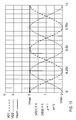
- the curves are obtained from Equation (1) applied to two voltages VD1 and VD2 detected with unitary modules at respective points spaced ⁇ /4 apart. The detection points span with continuity values from 0 to A.
- the summation curve Vsum VD1 + VD2 has a constant value of 2V.
- Fig.12 shows an embodiment of the power detector of the previous fig.9A for a particular rectangular waveguide comprised of a metallic body 14 with a longitudinal slot 14' of rectangular cross-section, shaped as the cavity of a rectangular waveguide deprived of a side-wall, which is replaced by a uniform metallization laid down on a bottom face of a dielectric substrate 15, tightly screwed to the metallic body of waveguide 14 by means of a double row of screws 16 parallel to the longitudinal axis.
- Fig.13 shows an enlarged representation of two narrow irises S1 and S2 etched on the metallized side-wall 20 of waveguide 14.
- the two irises are aligned along the centre line of the side-wall with their middle points spaced ⁇ /4 to each other at the centre of the operating frequency band.
- the two irises S1 and S2 are depicted in relation to the directions of electric and magnetic fields E, H inside the cavity 14' of waveguide 14.
- the two irises in figure are directed along the lines of the H field to obtain an inductive coupling.
- the two irises are 0.2 mm width and 4.5 mm long.
- the circuital layout of power detector is obtained using the well known printed circuit board (PCB) technology.
- the upper layout includes two microstrips L1 and L2, each one intersecting a respective iris S1 or S2 orthogonally, magnetically coupled to the magnetic field inside the waveguide.
- the intersection lines pass over the middle points of S1 and S2, thus L1 and L2 are parallel and are spaced ⁇ /4 apart evaluated in correspondence of the central frequency of the working band.
- Microstrips L1 and L2 are grounded at one end immediately beyond the crossed irises S1 and S2, whereas the other end is soldered to the anode of a respective Schottky diode D1 and D2.
- the cathode of D1 and D2 are RF grounded by quarter-wave low-impedance open-stubs (which replace the capacitor C of figures 4 and 5 and C1, C2 of fig.8B )
- the length of microstrips L1 and L2 is also ⁇ /4 so as to show an open circuit impedance on the anode of the diodes.
- a ⁇ /4 line connects the cathode of diode D1 to an end of a resistor R1, the same is valid for diode D2 and a resistor R2 with the same value as R1.
- the other end of R1 and R2 are connected to a summing node 19 corresponding to the point of confluence of two paths 17 and 18 departing from the other end of resistor R1 and R2.
- Diodes and resistors are discrete devices picked and placed on the substrate and soldered using the surface mount technology (SMT). Other devices might be connected to this base scheme for thermal compensation and duplication of voltage Vsum.
- the degree of coupling between the waveguide 14 and each of the two lines L1 and L2 has been calculated (using simulation software Ansoft HFSS ® ) and the results versus frequency are plotted in fig.14 .
- Let Pi the power of microwave signal in transit through the waveguide 14, and Pacc the power captured by an iris, the coupling is calculated as: Acc 10*Log Pi/Pacc.
- the curves in figure show that the power captured by each iris is on the average 20 dB below the power in transit through the waveguide 14, so the power detector does not subtract significant power from the signal.
- the frequency behaviour of power detector of fig.12 has been tested manufacturing a prototype arranged as a test fixture that includes a tract of waveguide 14 (with screwed the substrate 15) between two SMA transitions screwed at the ends.
- One SMA port is connected to an RF signal generator, the other one is connected to different loads to obtain different return loss values.
- the worst-case is experimented when the output port is left open.
- the frequency of signal generator is varied with continuity in the range from 14.5 to 15.5GHz, corresponding to the band of interest, and in correspondence the voltage VD1, VD2, and Vsum ( fig.9B ) are measured.
- the text fixture provides relevant measuring points to be accessed from the external.
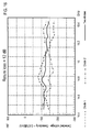
- the results of the measures ranked for decreasing matching conditions are shown in the successive figures 15 to 18 .
- the ripple is also a measure of the maximum error in the detection.
- the second curve is always under the first one of at least 0.5 dB but for values of ⁇ below 0.3 the ripple is null for the two curves. This encompasses all practical cases where a good matching is required, as a consequence the importance of optimizing the spacing over ⁇ /4 should be considered as a secondary improvement.
- the previous concepts are resumed in the following table. TABLE 2. Return Loss (dB) ⁇ Standing Wave Ratio (dB) Maximum Detector Error (dB) 6 0.5 9.5 0.5 12 0.25 4.4 0 18 0.125 2.18 0 24 0.063 1.06 0
Landscapes
- Engineering & Computer Science (AREA)
- Power Engineering (AREA)
- Physics & Mathematics (AREA)
- General Physics & Mathematics (AREA)
- Microwave Amplifiers (AREA)
Abstract
A Microwave power detector is coupled to a rectangular waveguide with a sidewall replaced by an uniform metallization on a bottom face of a FR4 dielectric substrate screwed to the waveguide. Two irises aligned along a common line parallel to the lines of magnetic field inside the waveguide, are etched inside the metallization acting as sidewall. Two microstrips are laid down on the upper face of dielectric substrate, each one intersects a respective iris orthogonally in the middle point. The two microstrips are connected to ground at one end immediately beyond respective irises, and are spaced substantially quarter wave apart calculated at the centre of the operating frequency band (15-18 GHz). Besides, the two microstrips are quarter wave long in order to show an open circuit impedance at the other end connected to a respective voltage detector including a Schottky diode in series to a resistor. At midpoint of the connection line between the two serially connected voltage detectors a voltage Vsum is read with high impedance. Vsum is the average of the two detected voltages, it is indicative of the signal power travelling across the waveguide and it results substantially insensitive of standing-wave pattern (fig.12 ).
Description
- The present invention relates to the field of microwave power detection, and more precisely to a microwave power detector insensitive to standing-wave pattern of a mismatched waveguide transmitted microwave signal. As known, power detection is directly related to voltage detection at the ends of a known resistor; being V the mean detected voltage and P the average power across the waveguide, it results in the linear law relationship of a diode detector: P = V2 /R or

-
Fig.1 schematizes a final part of a microwave transmitter before the antenna system (not shown). This arrangement comprises apower stage 1 connected to a first end T1 of a transmission line M/W (either microstrip or waveguide) with the other end T2 connected to an input port of aduplexer filter 2. The configuration offig.1 is used in a lot of radio transmission systems, e.g.: line-of-sight radio links, point-to-point or point-to-multipoint multipath transmission systems like mobile radio networks or MAN/LAN 802.16 networks, etc. The present invention is valid both for wireless or wired transmission systems. A general problem of these systems is that of knowing by a control unit the exact power transmitted from the power stage, in order to perform a procedure called Remote Transmit Power Control (RTPC) that is needed to regulate the power level inside the foreseen dynamic. In line of principle the transmitted power level should be read by placing a detector in a suitable position along the M/W transmission line close to thepower stage 1, but this is not enough as the following theory will demonstrate. - Without limitation, the characteristic impedance ZO of line M/W is 50 Ohm. The input impedance of the
duplexer filter 2 represents the load impedance ZL at the end T2 of transmission line M/W. If ZL is matched to 50 Ohm of the line the RF power at the end T2 is not reflected back towards T1, otherwise a power fraction only depending on ZL is reflected back towards theamplifier 1. More in general, saying γ = α + jβ the propagation constant of the travelling wave along the line M/W, and adopting the phasor notation hiding the time-dependent term e-jωt , and using the variable z to indicate distances from the load ZL located at z = 0, if a voltage wave V+e-γz with an associated current I + e-γz is incident on the termination load, a reflected voltage V-eγz with a current -I-eγz will, in general, be created. Hence on the load ZL it results V = V+ + V- = VL , I = I+ -I- = IL and by definition ZL = VL /IL . The ratio of V - to V + is usually described by a complex voltage reflection coefficient
Z L =ZL /Z0 is defined the normalized load impedance. After a certain handling we obtain:
fig.1 ). Let Γ = pejθ and, consequently, ρ = |Γ| , after a trigonometrical handling we obtain:

- In the case of lossy line with attenuation constant α, the previous equation hold except that jβ must be replaced by α + jβ . In application with waveguides α is so small that for the short lengths the neglect of α is justified. The effect of α shall be considered when high losses FR4 substrates are used. Clearly the presence of an attenuation constant α does not affect the definition of the voltage reflection coefficient Γ L for the load connected at the end T2. However, at any other point a distance l toward the end T1, the reflection coefficient is now given by: Γ(l) = Γ Le -2jβl-2 αl. As l is increased, Γ decreases exponentially until, for large l, it essentially vanishes.
- The theory developed above demonstrates that in wave guides (or transmission lines in general), limitedly to an ideal case without any mismatch and losses, the voltage module is constant along the transmission line, so that the position of a detector is indifferent, but this is only an exception because the real behaviour of the system of
fig.1 is very different from the ideal and by way of mismatching a standing-wave pattern is generally present. In this case the microwave detector provides a voltage signal strongly dependent from the nodes and antinodes position on the line in respect to the detector position. Nodes and antinodes move on the line as the frequency or terminal impedances change and, as a consequence, the detected voltage is not representative of the available power.TABLE 1 reports some comparative values of the most representative parameters of mismatch. Return Loss (dB) Reflection coefficient (ρ) Standing Wave Ratio (dB) 0 1 ∞ 6 0.5 9.5 12 0.25 4.4 18 0.125 2.18 24 0.063 1.06 ∞ 0 1 - Up to now the problem of a reliable power detection has been solved by the use of a high directivity directional coupler inclusive of a voltage detector able to detect the travelling wave toward the load (duplexer 2) and not the one in opposite direction. Unfortunately the high directivity directional coupler, in principle, is easy to do in wave guide but in practice not used for its considerable dimension, difficult working and assembling time. Microstrip couplers, instead, exhibit poor directivity unless made half wave long, but, as a consequence, noteworthy insertion loss will be produced if a standard high loss dielectric substrate (e.g. FR4) is used. Finally, low directivity directional couplers quarter wave long is allowed, but the use of an isolator is mandatory in order to avoid the reflected wave. In this case the isolators cost has to be taken into consideration. The two options are depicted in
fig.2 , for half wave, and infig.3 for quarter wave implementations. In these figures we see apower detection circuit 3 comprising a directional coupler 3' coupled to the transmission line M/W nearby its end T1 for capturing a small fraction of the transmitted signal that is forwarded to avoltage detector 3". Infig.3 acirculator 4 is coupled between the end T2 of transmission line M/W and the input ofduplexer filter 2. -
Fig.4 shows a realization of thepower detector circuit 3 with microstrip coupler. This power detector includes a 4-port directional coupler HYB (hybrid) connected to some discrete devices. The hybrid HYB is constituted of two half wave parallel microstrips M1, M2 opportunely spaced to each other so as to be coupled; a first microstrip being a tract of the transmission line M/W (microstrip) in proximity of the end T1. The four ports are numbered as 1, 2, 3, 4.Port 1 is located near to the end T1;port 2 is λ/2 apart on microstrip M/W;port 3 is an end of the microstrip M2 at the same side ofport 1, andport 4 is λ/2 apart onmicrostrip M2. Port 3 is connected to a load resistor Ro = 50 Ohm, the other end of resistor Ro is grounded.Port 4 is connected to the anode of a diode D1 whose cathode is connected to the parallel of a resistor R and a capacitor C both grounded at the other end. The diode D1 connected to R and C constitutes a rectifying circuit for the microwave signal able to generate a rectified voltage VD across resistor R. The capacitor C is charged to the average rectified voltage. If the hybrid HYB works ideally,port 3 is decoupled from the transmitted signal Pi andport 4 is coupled instead. Dually,port 4 is decoupled from the reflected signal present atport 2, andport 3 is coupled so as to dissipate the reflected signal on the load resistor Ro. In the reality a small power ratio of signal Pi is also coupled to theisolated port 3 and a small power ratio of the reflected signal is also coupled toport 4. The spurious couplings worsen the directivity of thevoltage detector 3 and hence the truthfulness of detection. -
Fig.5 shows an alternativepower detector circuit 3 that differs from the one illustrated infig.4 by way of quarter wave length of microstrips M1, M2 instead of half wave. In thiscase port 4 andport 3 invert their rules, so the rectifying circuit D1, R, and C is connected toport 3 and Ro is connected toport 4. - Comparative curves of coupling and directivity versus frequency of the two directional couplers depicted in
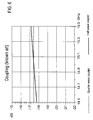
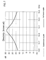
figures 4 and5 are shown infigures 6 and7 . With reference tofig.6 , we see that coupling is nearby the same for the two types of directional couplers but a large gap exists between the directivity curves shown infig.7 , being the quarter wave coupler poor directive, and the use of circulator is plenty justified. - A useful tool for studying directional couplers and microwave n-port circuits in general is the so-called scattering matrix S having the following representation

where apex - and + indicate signals outgoing from or incoming to two transmission lines respectively connected to the ports indicated bysubscript fig.4 ,ports 1 an 2 are the input and output port, respectively, whileports - The object of the present invention is that to overcome the defects of microwave power detector of the prior art discussed with reference to the preceding figures, and indicate a microwave power detector insensitive to the standing-wave pattern, as far as possible. The insensitive microwave power detector should be applicable to a transmission line in general, either a closed-type waveguide or an open-type line such as microstrips or balanced coplanar lines.
- The invention achieves said object by providing a microwave detector of the signal power travelling across a transmission line, as disclosed in
claim 1. - According to the invention, the microwave power detector includes:
- first and second coupling means spaced along a coupled transmission line substantially quarter wave apart at the centre of the operating frequency band;
- first and second voltage detection means respectively connected to said first and second coupling means for providing a voltage indicative of said travelling power;
- adding means connected to the output of both voltage detection means for providing a detected voltage indicative of said travelling power and substantially insensitive of standing-wave pattern changes.
- Additional features of the present invention which are believed to be novel are set forth with particularity in the appended claims.
- According to the invention, the adding means is more simply a point (midpoint) of the connection between the first and the second voltage detection means. It is easily proved that this type adding means obtain the average between the two detected (rectified) voltages.
- According to a preferred embodiment of the invention, said transmission line is a rectangular waveguide with a side-wall replaced by an uniform metallization on a face of a dielectric substrate fixedly connected to the waveguide, and the coupling means includes:
- two irises opened on said metallization acting as side-wall, being the irises aligned along a common line parallel to the lines of magnetic field inside the waveguide;
- two microstrips on the opposite face of dielectric substrate in respect of the uniform metallization, each microstrip intersecting a respective iris orthogonally.
- This arrangement forces the microstrips to be parallel and to be spaced quarter wave apart. According to the invention, the following features are considered as profitable:
- The two microstrips cross the irises at the centre
- The two microstrips are connected to ground at one end immediately beyond the respective irises.
- The two microstrips are quarter wave long in order to show an open circuit impedance at the other end connected to the voltage detectors.
- A low-cost high loss FR4 dielectric substrate is used to obtain the metallization acting as side-wall for the waveguide and ground plane for all microstrips of the two voltage detectors.
- The dielectric substrate is tightly screwed to the metallic waveguide.
- Surface mount technology (SMT) is used to connect the diodes and the other discrete devices used in the voltage detectors.
- Thanks to the invention the detected voltage at the output of the adder node only depends on the signal power conveyed by the transmission line, remaining insensitive to the standing-wave pattern whose amplitude is correlated to the mismatching value.
- The advantages are evident especially when a waveguide is available for placing the power detector. In such a way couplers and/or isolators can be missed with considerable cost saving in terms of material and assembling time. Moreover the absence of detection circuits at the output of the power stage allows to minimize the path to the microstrip-waveguide transition.
- The features of the present invention which are considered to be novel are set forth with particularity in the appended claims. The invention and its advantages may be understood with reference to the following detailed description of an embodiment thereof taken in conjunction with the accompanying drawings given for purely non-limiting explanatory purposes and wherein:
-
fig.1 , already described, indicates a RF power stage of the microwave transmitter of the prior art; -
figures 2 and 3 , already described, indicate two conventional configurations of power detector coupled to the power stage offig.1 ; -
figures 4 and5 , already described, indicate two possible known configurations of a directional coupler belonging to the power detector offigures 2 and 3 ; -
figures 6 and7 , already described, indicates comparative curves of coupling and directivity versus frequency of both directional couplers offigures 4 and5 ; -
fig.8A indicates a balanced transmission line schematisation of the power detector of the present invention; -
fig.8B indicates a microstrip circuital schematisation embodied with hybrids of the power detector of the present invention; -
fig.9A indicates a waveguide circuital schematisation of the power detector of the present invention; -
fig.9B indicates the equivalent electrical circuit of the power detector offig.9A ; -
fig.10 indicates a microstrip to waveguide transition at the output of the power detector offig.9A ; -
fig.11 indicates two standing-wave patterns as detectable by two voltage detectors spaced quarter wave apart, both included in the configuration offig.8A, 8B ,9A if a wavelength is spanned along an ideal lossless transmission line; the constant pattern summation voltage is also indicated; -
fig.12 indicates with more detail the embodiment of the waveguides power detector offig.9A ; -
fig.13 shows a particular of two irises included in the embodiment offig.12 ; -
fig.14 reports the curves of coupling vs .frequency referred to each iris; -
figures 15 to 18 reports comparative curves of the voltage vs. frequency at the output of two voltage detectors and the average voltage at the summation node of the embodiment offig.12 ; -
fig.19 reports comparative curves of the detected voltage ripple amplitude (error) vs. module of reflection coefficient for two distances between the irises. - As a description rule, same elements in the drawings are referenced by the same labels, and the elements represented in the figures are not a scaled reproduction of the original ones.
- With reference to
fig.8A , we see a balanced transmission line BTL fed by a microwave generator and terminated with a load. A power fraction of direct wave across the line is reflected by the load because of impedance mismatch, with a reflection coefficient ρ depending on the entity of mismatch. Twovoltage detectors Capacitive coupling relevant voltage detector fig.8A can be easily modified to be used with unbalanced transmission line such as microstrips. - With reference to
fig.8B , we see a microstrip M1 used to convey a microwave transmission signal from the output of a RF power stage (not shown) towards the input of a duplexer filter. Along the microstrip M1 a second quarter wave power detector similar to the one offig.5 is replicated immediately after a first one placed nearby the output of the power stage. Replication is performed at the other side of microstrip M1 in a way that the length of the twofold structure is half wave at the central frequency of operating band. The two power detectors include two directional couplers hybrids HYB1 and HYB2. The four ports of HYB1 are numbered 1 to 4 as infig.5 . The four ports of HYB2 are numbered 5 to 8 with the same criterion adopted for HYB1. Theoutput port 2 of HYB1 also correspond to theinput port 5 of HYB1. The two hybrids are connected to two voltage detectors including Schottky diodes D1 and D2 serially connected to respective R1, C1 and R2, C2 networks. Two quasi-constant voltages VD1 and VD2 are present at the output of the two voltage detectors, the values of VD1 and VD2 depend on the dynamic of standing-wave pattern on the microstrip M1 detected at the positions corresponding to the coupledports fig.11 . Voltages VD1 and VD2 are summed up at theanalog adder 11 obtaining a voltage Vsum insensible to the amplitude of standing-wave pattern, as resulting from those figures. - With reference to
fig.9A , we see amicrowave power stage 1 coupled to an end T1 of a short microstrip M having the other end T2 coupled to an end of a waveguide W used to convey the microwave transmission signal towards the other end T3 coupled to the input of aduplexer filter 2. The end T2 includes a transition between the microstrip M to the waveguide W. First coupling means 5 (inductive/capacitive iris, probe, or equivalent means) is placed to the waveguide W in proximity of the transition at T2. Thecoupler 5 transfers the captured microwave signal to amicrostrip 6 connected to avoltage detector 7. Spaced λg/4 from (the centre of)coupler 5, where λg is the wavelength of the fundamental propagation mode in the waveguide W, asecond coupler 8 is placed to the waveguide W. Thecoupler 8 transfers the captured microwave signal to amicrostrip 9 connected to avoltage detector 10. At the output of the twovoltage detectors analog adder 11, obtaining a voltage Vsum insensible to the amplitude of standing-wave pattern. - The equivalent electrical circuit of the power detector of the preceding figure is represented in
fig.9B . With reference to the figure, the equivalent circuit comprises two voltage detectors, a first one includes a voltage generator VD1 connected in series to a resistors R1, a second one includes a voltage generator VD2 connected in series to a resistors R2 of equal value. The two voltage generators take care about the coupling voltage seen at the ends of respective resistors when the diodes are conducting. The other ends of resistors R1 and R2 are connected together. At a point of the connection between the two resistors a detected voltage Vsum is read with high impedance. Vsum corresponds to the average voltage (VD1 + VD2)/2 between VD1 and VD2; this result is independent from the concordant or discordant polarity of two diodes. It can be noticed in figure that, because of the high impedance of the reading device of the voltage Vsum, the two voltage detectors are connected in series. This is the case of an operational amplifier used to read Vsum and obtaining in the meanwhile thermal stabilization. -
Fig.10 shows in detail the microstrip to waveguide transition carried out at the microstrip end T2. With reference to the figure, we see the free end of microstrip M encircled by ametallization 12 laid down on adielectric substrate 13 having a ground plane on the other side.Metallization 12 lets uncovered a rectangular window in correspondence of the free end of microstrip M. The ground plane faced to the rectangular window is removed for permitting to the signal travelling on the microstrip M of being irradiated towards the mouth of waveguide W faced to the rectangular window (not visible in figure). This type of transition is well known in the art and the Applicant filed some patent applications in merit. -
Fig.11 shows two curves of standing-wave pattern spanning a wavelength A of an ideal lossless transmission line in case of total reflection (p = 1) by the load. The curves are obtained from Equation (1) applied to two voltages VD1 and VD2 detected with unitary modules at respective points spaced λ/4 apart. The detection points span with continuity values from 0 to A. The summation curve Vsum = VD1 + VD2 has a constant value of 2V. -
Fig.12 shows an embodiment of the power detector of the previousfig.9A for a particular rectangular waveguide comprised of ametallic body 14 with a longitudinal slot 14' of rectangular cross-section, shaped as the cavity of a rectangular waveguide deprived of a side-wall, which is replaced by a uniform metallization laid down on a bottom face of adielectric substrate 15, tightly screwed to the metallic body ofwaveguide 14 by means of a double row ofscrews 16 parallel to the longitudinal axis. -
Fig.13 shows an enlarged representation of two narrow irises S1 and S2 etched on the metallized side-wall 20 ofwaveguide 14. The two irises are aligned along the centre line of the side-wall with their middle points spaced λ/4 to each other at the centre of the operating frequency band. The two irises S1 and S2 are depicted in relation to the directions of electric and magnetic fields E, H inside the cavity 14' ofwaveguide 14. The two irises in figure are directed along the lines of the H field to obtain an inductive coupling. - With reference to
fig.12 and 13 , in an exemplary embodiment working at 15-18 GHz the two irises are 0.2 mm width and 4.5 mm long. On the upper face ofdielectric substrate 15 the circuital layout of power detector is obtained using the well known printed circuit board (PCB) technology. The upper layout includes two microstrips L1 and L2, each one intersecting a respective iris S1 or S2 orthogonally, magnetically coupled to the magnetic field inside the waveguide. The intersection lines pass over the middle points of S1 and S2, thus L1 and L2 are parallel and are spaced λ/4 apart evaluated in correspondence of the central frequency of the working band. Microstrips L1 and L2 are grounded at one end immediately beyond the crossed irises S1 and S2, whereas the other end is soldered to the anode of a respective Schottky diode D1 and D2. The cathode of D1 and D2 are RF grounded by quarter-wave low-impedance open-stubs (which replace the capacitor C offigures 4 and5 and C1, C2 offig.8B ) The length of microstrips L1 and L2 is also λ/4 so as to show an open circuit impedance on the anode of the diodes. A λ/4 line connects the cathode of diode D1 to an end of a resistor R1, the same is valid for diode D2 and a resistor R2 with the same value as R1. The other end of R1 and R2 are connected to a summingnode 19 corresponding to the point of confluence of twopaths - The degree of coupling between the
waveguide 14 and each of the two lines L1 and L2 has been calculated (using simulation software Ansoft HFSS® ) and the results versus frequency are plotted infig.14 . Let Pi the power of microwave signal in transit through thewaveguide 14, and Pacc the power captured by an iris, the coupling is calculated as: Acc=10*Log Pi/Pacc. The curves in figure show that the power captured by each iris is on the average 20 dB below the power in transit through thewaveguide 14, so the power detector does not subtract significant power from the signal. - The frequency behaviour of power detector of
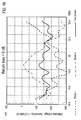
fig.12 has been tested manufacturing a prototype arranged as a test fixture that includes a tract of waveguide 14 (with screwed the substrate 15) between two SMA transitions screwed at the ends. One SMA port is connected to an RF signal generator, the other one is connected to different loads to obtain different return loss values. The worst-case is experimented when the output port is left open. The frequency of signal generator is varied with continuity in the range from 14.5 to 15.5GHz, corresponding to the band of interest, and in correspondence the voltage VD1, VD2, and Vsum (fig.9B ) are measured. The text fixture provides relevant measuring points to be accessed from the external. The results of the measures ranked for decreasing matching conditions are shown in the successivefigures 15 to 18 . - With reference to
fig.15 and TABLE 1, under the maximum matching condition for ρ = 0 the three curves are substantially coincident, this is in line with the average for Vsum, and the voltage Vsum is substantially flat in the band of measure. The successivefigures 16 to 18 show that despite an increasing variation of VD1 and VD2, the voltage Vsum undergoes a remarkable lower variation; this is also true for the total reflection case offig.18 . - The theoretical curves represented in
fig.11 for ρ = 1 might be calculated for any other value of ρ but the conclusions should be always the same, to say, under ideal conditions (no impedance variation with frequency) the spacing of λ/4 between two detection points along the transmission line allows to obtain the sum of the two individual detected voltages the most independent as possible from the position of the two irises. Owing to non-idealities, this statement is not completely true and perhaps a separation slightly greater than λ/4 between detection points could be better.Fig.19 is a demonstration of this fact. In this figure two curves of the ripple of Vsum (mV) over the constant value versus the reflection coefficient ρ are reported; a first curve accounts for 0.25 λ spacing and a second curve for 0.30 λ spacing. The ripple is also a measure of the maximum error in the detection. With reference tofig.19 , we see that the second curve is always under the first one of at least 0.5 dB but for values of ρ below 0.3 the ripple is null for the two curves. This encompasses all practical cases where a good matching is required, as a consequence the importance of optimizing the spacing over λ/4 should be considered as a secondary improvement. The previous concepts are resumed in the following table.TABLE 2. Return Loss
(dB)ρ Standing Wave Ratio
(dB)Maximum Detector Error
(dB)6 0.5 9.5 0.5 12 0.25 4.4 0 18 0.125 2.18 0 24 0.063 1.06 0 - Although the invention has been described with particular reference to a preferred embodiment, it will be evident to those skilled in the art, that the present invention is not limited thereto, but further variations and modifications may be applied without departing from the scope of the claims.
Claims (14)
- Microwave detector of the signal power travelling across a transmission line, including:- first coupling means (HYB1; S1, L1) coupled to said transmission line (M1; 14, 14', 15);- first voltage detection means (D1, R1) connected to said first coupling means for providing a first voltage (VD1) indicative of said travelling power,characterized in that further comprises:- second coupling means (HYB2; S2, L2) coupled to said transmission line at a distance from said first coupling means substantially quarter wave long at the centre of the operating frequency band;- second voltage detection means (D2, R2) connected to said second coupling means for providing a second voltage (VD2) indicative of said travelling power;- adding means (11, 19) connected to the output of both voltage detection means for providing a third voltage (Vsum) indicative of said travelling power and substantially insensitive of standing-wave pattern.
- The microwave power detector of claim 1, characterized in that: said adding means (11, 19) correspond to a point of the connection between said first (D1, R1) and second (D2, R2) voltage detection means.
- The microwave power detector of claim 2, characterized in that said first (D1, R1) and second (D2, R2) voltage detection means (D2, R2) each includes a Schottky diode in series to a resistor, being the central point of the series grounded at radiofrequency by a quarter-wave low-impedance open-stub.
- The microwave power detector of any claim from 1 to 3, characterized in that:- said transmission line is a rectangular waveguide (!4, 14', 15) with a side-wall replaced by an uniform metallization (20) on a face of a dielectric substrate (15) fixedly connected (16) to the waveguide,and said first and second coupling means includes:- two irises (S1, S2) opened on said metallization acting as side-wall, being the irises aligned along a common line parallel to the lines of magnetic field inside the waveguide;- two microstrips (L1, L2) on the opposite face of dielectric substrate (15) in respect of the uniform metallization (20), each microstrip intersecting a respective iris orthogonally.
- The microwave power detector of claim 4, characterized in that said microstrips (L1, L2) are spaced quarter wave apart.
- The microwave power detector of claim 4 or 5, characterized in that said microstrips (L1, L2) cross the respective irises (S1, S2) at their centre.
- The microwave power detector of any claim from 4 to 6, characterized in that said microstrips (L1, L2) are connected to ground at one end immediately beyond the respective irises (S1, S2).
- The microwave power detector of claim 7, characterized in that said microstrips (L1, L2) are quarter wave long in order to show an open circuit impedance at the other end connected to said voltage detection means.
- The microwave power detector of any claim from 4 to 8, characterized in that for an operating frequency band of 15-18 GHz said irises (S1, S2) are 0.2 mm width and 4.5 mm long.
- The microwave power detector of any claim from 4 to 9, characterized in that said dielectric substrate (15) has high dielectric losses as the FR4 used in printed circuit board technology.
- The microwave power detector of any claim from 4 to 10, characterized in that said dielectric substrate (15) is tightly screwed (16) to the rectangular waveguide (14).
- The microwave power detector of any claim from 1 to 3, characterized in that:- said transmission line is a first microstrip (M1);- said first coupling means includes a first quarter wave directional coupler (HYB1) comprising a second microstrip (M2) parallel to the first microstrip (M1);- said second coupling means includes a second quarter wave directional coupler (HYB2) comprising a third microstrip (M3) parallel and contiguous to the second microstrip (M2) at the other side of the first microstrip (M1).
- The microwave power detector of claim 12, characterized in that said voltage detection means (D2, R1, D2, R2) are respectively connected to a coupled port (3, 7) of the first (HYB1) and the second (HYB2) quarter wave directional couplers.
- The microwave power detector any claim from 1 to 3, characterized in that:- said transmission line (BTL) is balanced;- said first and second coupling means include capacitive coupling (5, 5'; 8, 8') at each cross-point between the balanced transmission line (BTL) and a respective connection line directed to an end of a voltage detector (7, 10) connected across the balanced transmission line (BTL);- said adding means includes balanced inputs.
Priority Applications (1)
| Application Number | Priority Date | Filing Date | Title |
|---|---|---|---|
| EP07425028A EP1947464A1 (en) | 2007-01-22 | 2007-01-22 | Power detector insensitive to standing waves of a microwave signal transmitted by a mismatched waveguide |
Applications Claiming Priority (1)
| Application Number | Priority Date | Filing Date | Title |
|---|---|---|---|
| EP07425028A EP1947464A1 (en) | 2007-01-22 | 2007-01-22 | Power detector insensitive to standing waves of a microwave signal transmitted by a mismatched waveguide |
Publications (1)
| Publication Number | Publication Date |
|---|---|
| EP1947464A1 true EP1947464A1 (en) | 2008-07-23 |
Family
ID=38179536
Family Applications (1)
| Application Number | Title | Priority Date | Filing Date |
|---|---|---|---|
| EP07425028A Withdrawn EP1947464A1 (en) | 2007-01-22 | 2007-01-22 | Power detector insensitive to standing waves of a microwave signal transmitted by a mismatched waveguide |
Country Status (1)
| Country | Link |
|---|---|
| EP (1) | EP1947464A1 (en) |
Cited By (6)
| Publication number | Priority date | Publication date | Assignee | Title |
|---|---|---|---|---|
| US9461755B2 (en) | 2014-01-17 | 2016-10-04 | Viasat, Inc. | Enhanced voltage standing wave ratio measurement |
| RU2693868C1 (en) * | 2018-12-07 | 2019-07-05 | Акционерное общество "Научно-производственная фирма "Микран" | Superhigh-frequency signal power diode detector |
| EP3579408A1 (en) | 2018-06-08 | 2019-12-11 | Diehl Defence GmbH & Co. KG | Radiation source for microwave pulse and radiating device |
| CN111239578A (en) * | 2020-01-19 | 2020-06-05 | 中国电子科技集团公司第十三研究所 | Power tube test fixture and preparation method thereof |
| CN113267672A (en) * | 2021-05-06 | 2021-08-17 | 南京邮电大学 | 6G communication microwave power detection system based on radio frequency diode |
| CN117949727A (en) * | 2024-03-25 | 2024-04-30 | 深圳市瀚强科技股份有限公司 | Microwave wavelength detection device and microwave output equipment |
Citations (3)
| Publication number | Priority date | Publication date | Assignee | Title |
|---|---|---|---|---|
| EP1296146A1 (en) * | 2001-09-21 | 2003-03-26 | Alcatel | RF signal detector circuit with reduced sensitivity to transmission line impedance mismatches |
| US6803754B2 (en) * | 2000-08-14 | 2004-10-12 | Rohde & Schwarz Gmbh & Co. Kg | Power sensor |
| US20050116701A1 (en) * | 2002-02-08 | 2005-06-02 | Rohde& Schwarz Gmbh & Co. Kg | Power detector with constant voltage decoupling |
-
2007
- 2007-01-22 EP EP07425028A patent/EP1947464A1/en not_active Withdrawn
Patent Citations (3)
| Publication number | Priority date | Publication date | Assignee | Title |
|---|---|---|---|---|
| US6803754B2 (en) * | 2000-08-14 | 2004-10-12 | Rohde & Schwarz Gmbh & Co. Kg | Power sensor |
| EP1296146A1 (en) * | 2001-09-21 | 2003-03-26 | Alcatel | RF signal detector circuit with reduced sensitivity to transmission line impedance mismatches |
| US20050116701A1 (en) * | 2002-02-08 | 2005-06-02 | Rohde& Schwarz Gmbh & Co. Kg | Power detector with constant voltage decoupling |
Cited By (11)
| Publication number | Priority date | Publication date | Assignee | Title |
|---|---|---|---|---|
| US9461755B2 (en) | 2014-01-17 | 2016-10-04 | Viasat, Inc. | Enhanced voltage standing wave ratio measurement |
| EP3579408A1 (en) | 2018-06-08 | 2019-12-11 | Diehl Defence GmbH & Co. KG | Radiation source for microwave pulse and radiating device |
| DE102018004568A1 (en) | 2018-06-08 | 2019-12-12 | Diehl Defence Gmbh & Co. Kg | Radiation source for microwave pulses and radiation device |
| US11209247B2 (en) | 2018-06-08 | 2021-12-28 | Diehl Defence Gmbh & Co. Kg | Radiation source for microwave pulses and radiation device |
| DE102018004568B4 (en) | 2018-06-08 | 2024-02-01 | Diehl Defence Gmbh & Co. Kg | Radiation source for microwave pulses and radiation device |
| RU2693868C1 (en) * | 2018-12-07 | 2019-07-05 | Акционерное общество "Научно-производственная фирма "Микран" | Superhigh-frequency signal power diode detector |
| WO2020117101A1 (en) * | 2018-12-07 | 2020-06-11 | Акционерное общество "Научно-производственная фирма "Микран" | Diode detector of microwave signal power |
| CN111239578A (en) * | 2020-01-19 | 2020-06-05 | 中国电子科技集团公司第十三研究所 | Power tube test fixture and preparation method thereof |
| CN113267672A (en) * | 2021-05-06 | 2021-08-17 | 南京邮电大学 | 6G communication microwave power detection system based on radio frequency diode |
| CN117949727A (en) * | 2024-03-25 | 2024-04-30 | 深圳市瀚强科技股份有限公司 | Microwave wavelength detection device and microwave output equipment |
| CN117949727B (en) * | 2024-03-25 | 2024-06-04 | 深圳市瀚强科技股份有限公司 | Microwave wavelength detection device and microwave output equipment |
Similar Documents
| Publication | Publication Date | Title |
|---|---|---|
| US6483397B2 (en) | Tandem six port 3:1 divider combiner | |
| US6600307B2 (en) | Method and apparatus for measuring true transmitted power using a broadband dual directional coupler | |
| CN113258244B (en) | Rectangular waveguide microstrip 0-degree-phase-difference high-isolation broadband power divider | |
| US5303419A (en) | Aperture-coupled line Magic-Tee and mixer formed therefrom | |
| CN112909471B (en) | A High Isolation Rectangular Waveguide-Microstrip Power Divider | |
| CN102361151B (en) | Asymmetrical coplanar waveguide cross directional coupler | |
| CN110233320A (en) | Present formula suspended stripline waveguide transitions structure in side | |
| EP0391596B1 (en) | Reduced-height waveguide-to-microstrip transition | |
| Ghanadi | A new compact broadband radial power combiner | |
| US7221181B2 (en) | Directional power detection by quadrature sampling | |
| US20050258917A1 (en) | Microstrip directional coupler | |
| Dang et al. | An ultra-wideband power combining in ridge waveguide for millimeter wave | |
| CN114938207A (en) | A Broadband Josephson Parametric Amplifier Chip Combined with Multi-section Impedance Transformers | |
| US4361819A (en) | Passive semiconductor power limiter formed on flat structure lines, and an ultra-high frequency circuit using such a limiter | |
| CN113612000B (en) | Rectangular waveguide I-shaped isolation network double-microstrip converter | |
| US4124823A (en) | Microwave coupler | |
| KR100578280B1 (en) | Asymmetric Wilkinson Power Divider with Simple Rectangular Fault Ground Structure | |
| CN109301419B (en) | Coplanar waveguide ultra-wideband sum-difference device | |
| CN110311201A (en) | A kind of reversed-phase power combiner | |
| KR100706211B1 (en) | Transmission structure inverter | |
| Ohira et al. | Dipole antenna pair revisited from kQ product and Poincare distance for wireless power transfer invited | |
| CN116314165B (en) | A millimeter-wave broadband balanced zero-bias detection chip based on Schottky barrier diode | |
| Zhang et al. | A flexible non-radiative dielectric waveguide with a 1-dB loss PCB-to-NRD coupler for mm-wave array applications | |
| US6414574B1 (en) | Potential-free connection for microwave transmission line | |
| EP2602861B1 (en) | High directivity directional coupler |
Legal Events
| Date | Code | Title | Description |
|---|---|---|---|
| PUAI | Public reference made under article 153(3) epc to a published international application that has entered the european phase |
Free format text: ORIGINAL CODE: 0009012 |
|
| AK | Designated contracting states |
Kind code of ref document: A1 Designated state(s): AT BE BG CH CY CZ DE DK EE ES FI FR GB GR HU IE IS IT LI LT LU LV MC NL PL PT RO SE SI SK TR |
|
| AX | Request for extension of the european patent |
Extension state: AL BA HR MK RS |
|
| AKX | Designation fees paid | ||
| REG | Reference to a national code |
Ref country code: DE Ref legal event code: 8566 |
|
| STAA | Information on the status of an ep patent application or granted ep patent |
Free format text: STATUS: THE APPLICATION IS DEEMED TO BE WITHDRAWN |
|
| 18D | Application deemed to be withdrawn |
Effective date: 20090124 |