EP1943670B1 - Semiconductor device - Google Patents
Semiconductor device Download PDFInfo
- Publication number
- EP1943670B1 EP1943670B1 EP06809507A EP06809507A EP1943670B1 EP 1943670 B1 EP1943670 B1 EP 1943670B1 EP 06809507 A EP06809507 A EP 06809507A EP 06809507 A EP06809507 A EP 06809507A EP 1943670 B1 EP1943670 B1 EP 1943670B1
- Authority
- EP
- European Patent Office
- Prior art keywords
- substrate
- epitaxial layer
- semiconductor
- layer
- region
- Prior art date
- Legal status (The legal status is an assumption and is not a legal conclusion. Google has not performed a legal analysis and makes no representation as to the accuracy of the status listed.)
- Not-in-force
Links
Images

Classifications
-
- H—ELECTRICITY
- H10—SEMICONDUCTOR DEVICES; ELECTRIC SOLID-STATE DEVICES NOT OTHERWISE PROVIDED FOR
- H10P—GENERIC PROCESSES OR APPARATUS FOR THE MANUFACTURE OR TREATMENT OF DEVICES COVERED BY CLASS H10
- H10P90/00—Preparation of wafers not covered by a single main group of this subclass, e.g. wafer reinforcement
- H10P90/19—Preparing inhomogeneous wafers
- H10P90/1904—Preparing vertically inhomogeneous wafers
- H10P90/1906—Preparing SOI wafers
- H10P90/1914—Preparing SOI wafers using bonding
- H10P90/1916—Preparing SOI wafers using bonding with separation or delamination along an ion implanted layer, e.g. Smart-cut
-
- H—ELECTRICITY
- H10—SEMICONDUCTOR DEVICES; ELECTRIC SOLID-STATE DEVICES NOT OTHERWISE PROVIDED FOR
- H10D—INORGANIC ELECTRIC SEMICONDUCTOR DEVICES
- H10D30/00—Field-effect transistors [FET]
- H10D30/01—Manufacture or treatment
- H10D30/021—Manufacture or treatment of FETs having insulated gates [IGFET]
- H10D30/031—Manufacture or treatment of FETs having insulated gates [IGFET] of thin-film transistors [TFT]
- H10D30/0321—Manufacture or treatment of FETs having insulated gates [IGFET] of thin-film transistors [TFT] comprising silicon, e.g. amorphous silicon or polysilicon
- H10D30/0323—Manufacture or treatment of FETs having insulated gates [IGFET] of thin-film transistors [TFT] comprising silicon, e.g. amorphous silicon or polysilicon comprising monocrystalline silicon
-
- H—ELECTRICITY
- H10—SEMICONDUCTOR DEVICES; ELECTRIC SOLID-STATE DEVICES NOT OTHERWISE PROVIDED FOR
- H10W—GENERIC PACKAGES, INTERCONNECTIONS, CONNECTORS OR OTHER CONSTRUCTIONAL DETAILS OF DEVICES COVERED BY CLASS H10
- H10W10/00—Isolation regions in semiconductor bodies between components of integrated devices
- H10W10/10—Isolation regions comprising dielectric materials
- H10W10/181—Semiconductor-on-insulator [SOI] isolation regions, e.g. buried oxide regions of SOI wafers
-
- H—ELECTRICITY
- H10—SEMICONDUCTOR DEVICES; ELECTRIC SOLID-STATE DEVICES NOT OTHERWISE PROVIDED FOR
- H10D—INORGANIC ELECTRIC SEMICONDUCTOR DEVICES
- H10D86/00—Integrated devices formed in or on insulating or conducting substrates, e.g. formed in silicon-on-insulator [SOI] substrates or on stainless steel or glass substrates
- H10D86/01—Manufacture or treatment
- H10D86/021—Manufacture or treatment of multiple TFTs
- H10D86/0214—Manufacture or treatment of multiple TFTs using temporary substrates
Definitions
- the invention relates to a method of manufacturing a semiconductor device with a substrate and a semiconductor body comprising silicon which is provided with at least one semiconductor element, wherein an epitaxial semiconductor layer comprising silicon is grown on top of a first semiconductor substrate, wherein a splitting region is formed in the epitaxial layer, wherein a second substrate is attached by wafer bonding to the first substrate at the side of the epitaxial layer provided with the splitting region while an electrically insulating region is interposed between the epitaxial layer and the second substrate, the structure thus formed is split at the location of the splitting region as a result of which the second substrate forms the substrate with on top of the insulating region a part of the epitaxial layer forming the semiconductor body in which the semiconductor element is formed.
- the invention also relates to a semiconductor device obtained with such a - method and to manufacturing method for a semiconductor body suitable for use in such a method and to a semiconductor body obtained with such a method.
- other devices such as discrete devices are obtainable as well by such a method.
- a method as mentioned in the opening paragraph is known from JP-11-191617 that has been published on 13-07-1999.
- SOI Semiconductor On Insulator
- a method is proposed in which an epitaxial layer of silicon with a thickness in the range of 0,5 to 2,5 ⁇ m is provided on a first silicon substrate.
- an insulating region in the form of an oxide layer is formed on top of the epitaxial layer by thermal oxidation.
- a splitting region is formed in the epitaxial layer by implanting hydrogen ions through and below the oxide layer into the epitaxial layer.
- a second substrate of silicon is wafer bonded to the oxide layer on top of the epitaxial layer on the first substrate. After a splitting process in which the structure is ruptured at the splitting region the second substrate forms the substrate of the semiconductor device to be manufactured with on top of the insulating region a part of the epitaxial layer that forms a semiconductor body comprising silicon in which one or more semiconductor elements can be formed.
- the invention is based on the surprising recognition that the yield of the manufacturing of in particular high voltage FETs is limited by the fact that the gate oxide of these FETs on top of the part of the epitaxial layer has a varying thickness in lateral directions which e.g. causes local differences in electric field and charge capacitance behavior for transistors. These differences result in e.g. differences in leakage current or breakdown characteristics through which the yield is reduced.
- the invention further is based on the recognition that such a varying thickness of the gate oxide is caused by facets of certain pyramid shaped defects that cause a local different oxidation rate of the surface of the epitaxial layer.
- the thickness differences of the gate oxide normally a thermal oxide, decrease or even vanish if the temperature at which the gate oxide is formed, is increased. However, such increased temperature intervenes with requirements of a low thermal budget in advanced processes.
- the invention is based on the recognition that such defects can be removed by increasing the thickness of the epitaxial layer to a value between 5 and 15 ⁇ m.
- semiconductor devices with high voltage i.e. having operating voltages between 20 Volt and e.g. 150 Volt
- FETs are obtainable with a high yield.
- the splitting region is formed by a hydrogen implant at a distance from the surface of the epitaxial layer that lies between 0,05 and 2,0 micrometer. This implies that the semiconductor body comprising silicon has about the same thickness.
- the electrically insulating layer is deposited or grown on the second substrate before the wafer bonding. It has been found that in this way the yield of the manufacturing process is further improved. This can be explained by the fact that position of the splitting region can be formed in a more homogeneous and accurate manner since the implantation is not done through the insulating region because in this preferred embodiment said region is present on the other (second) substrate.
- the semiconductor element in particular the high voltage FET is formed in the part of the epitaxial layer remaining on top of the insulating layer which in turn is on top of the second substrate, e.g. by forming a thermal oxide on top of the silicon and forming a gate region on top thereof while source and drain regions are formed in the surface of the semiconductor body by suitable ion implantations that border - viewed in projection - the gate region.
- the invention further comprises a semiconductor device obtained with a method according to the invention.
- SOI Semiconductor On Insulator
- the semiconductor body obtained in this way forms in itself an attractive product since the device manufacture and the manufacture of the semiconductor body do not need to take place at one location or by one single manufacturer.
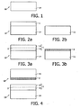
- Figs. 1 through 7 are sectional views of a semiconductor device at various stages in its manufacture by means of a method in accordance with the invention.
- Figs 1 through 7 are sectional views of a semiconductor device at various stages in its manufacture by-means of a method in accordance with the invention.
- the semiconductor device manufactured in this example is a high voltage field effect transistor.
- a first substrate 14, here of silicon is provided with (see Fig. 2a ) an epitaxial layer 1 comprising silicon, here of pure silicon, with a thickness of 12 ⁇ m.
- the deposition takes place at a pressure of 0.15 to 1 atm and a temperature of 1000 to 1200 °C.
- the epi layer 1 is here p-type doped with a doping concentration of about 10 15 at/cm 3 (specific resistance of about 13 ⁇ cm).
- a second substrate 11 is prepared, here also of silicon and with a standard thickness. Both substrates 11,14 are here of the p-type conductivity and have a doping concentration ranging from that of intrinsic material to e.g. about 10 15 at/cm 3 .
- a splitting region 2 is formed in the silicon epitaxial layer 1 on the first substrate 14. This is done by performing an implantation of hydrogen in the epi layer 1.
- said layer is "split" in two parts 1A,1B, the former having a thickness of 0.05 to 2.0 ⁇ m, in this example 1.5 ⁇ m, while the latter comprises about the remainder of the thickness of the epi layer 1.
- the implantation energy varies between 10 and 400 keV and is in this example 200 keV while the dose varies between 10 16 and 10 17 at/cm 2 and in this example is about 5 x 10 16 at/cm 2 .
- the second substrate 11 is provided with an electrically insulating layer 3, here in de form of a thermal silicon dioxide layer 3 which is provided by exposure to an oxygen containing ambient at a temperature of about 1050 °C.
- the oxide layer 3 obtained has a thickness of 0.1 to 1 ⁇ m and is in this example 1 ⁇ m thick.
- the second substrate 11 provided with the electrically insulating layer 3 is wafer bonded to the first substrate 14 at its side that is provided with the epitaxial layer 1 which in turn is already at this stage provided with the splitting region 2.
- the resulting structure is shown in Fig. 5 .
- the structure of Fig. 5 is subjected to a splitting treatment, which comprises heating of the structure to a temperature in the range of 500 to 600 °C, in this example at 500 °C in a furnace and under an atmosphere of N 2 at a pressure of 1 atm.
- a splitting treatment comprises heating of the structure to a temperature in the range of 500 to 600 °C, in this example at 500 °C in a furnace and under an atmosphere of N 2 at a pressure of 1 atm.
- the transistor T has gate oxide 4, here a thermal oxide of 30 nm on top of which a gate region 5, e.g. of polycrystalline silicon is formed. Aligned with the gate region 5 n-type source and drain regions 6,7 are formed in the silicon of the epilayer part 1A.
- the present invention is particularly suitable for the manufacture of (high-voltage) ICs like (C)MOS or BI(C)MOS ICs but also for bipolar ICs.
- VPE Vapor Phase Epitaxy
- MBE Molecular Beam Epitaxy
- ALE Atomic Layer Epitaxy
- CVD Chemical Vapor Deposition
- the epitaxial layer comprising silicon may comprise other materials like a mixed crystal of silicon and germanium.
- the splitting region may also be formed in another way, like by implanting helium ions in stead of hydrogen ions into the epitaxial layer.
Landscapes
- Recrystallisation Techniques (AREA)
- Thin Film Transistor (AREA)
- Element Separation (AREA)
Description
- The invention relates to a method of manufacturing a semiconductor device with a substrate and a semiconductor body comprising silicon which is provided with at least one semiconductor element, wherein an epitaxial semiconductor layer comprising silicon is grown on top of a first semiconductor substrate, wherein a splitting region is formed in the epitaxial layer, wherein a second substrate is attached by wafer bonding to the first substrate at the side of the epitaxial layer provided with the splitting region while an electrically insulating region is interposed between the epitaxial layer and the second substrate, the structure thus formed is split at the location of the splitting region as a result of which the second substrate forms the substrate with on top of the insulating region a part of the epitaxial layer forming the semiconductor body in which the semiconductor element is formed.
- The invention also relates to a semiconductor device obtained with such a - method and to manufacturing method for a semiconductor body suitable for use in such a method and to a semiconductor body obtained with such a method.
- Such a method is very suitable for making semiconductor devices like ICs (= Integrated Circuit). However, other devices such as discrete devices are obtainable as well by such a method.
- A method as mentioned in the opening paragraph is known from
JP-11-191617 - A drawback of such a method is that its yield of suitable semiconductor devices is rather low in case of semiconductor devices containing certain semiconductor elements, e.g. FETs and in particular high voltage FETs (= Field Effect Transistors).
- It is therefore an object of the present invention to avoid the above drawbacks and to provide a method, which results in devices, in particular those that contain high voltage FETs with a high yield.
- The invention is defined in the accompanying claims.
- The invention is based on the surprising recognition that the yield of the manufacturing of in particular high voltage FETs is limited by the fact that the gate oxide of these FETs on top of the part of the epitaxial layer has a varying thickness in lateral directions which e.g. causes local differences in electric field and charge capacitance behavior for transistors. These differences result in e.g. differences in leakage current or breakdown characteristics through which the yield is reduced.
- The invention further is based on the recognition that such a varying thickness of the gate oxide is caused by facets of certain pyramid shaped defects that cause a local different oxidation rate of the surface of the epitaxial layer. The thickness differences of the gate oxide, normally a thermal oxide, decrease or even vanish if the temperature at which the gate oxide is formed, is increased. However, such increased temperature intervenes with requirements of a low thermal budget in advanced processes. Finally, the invention is based on the recognition that such defects can be removed by increasing the thickness of the epitaxial layer to a value between 5 and 15 µm.
- Best results were obtained with a thickness value between 7 and 13 µm. Although higher thickness values are suitable as well, they increase the process time and are therefore to be avoided. This is quite surprisingly since the defects in question vary in size from 0,3 to 1,3 µm and one thus would expect that the influence of such defects would be vanished already at the usual thickness for the epitaxial layer.
- With a method according to the invention semiconductor devices with high voltage, i.e. having operating voltages between 20 Volt and e.g. 150 Volt, FETs are obtainable with a high yield.
- Preferably the splitting region is formed by a hydrogen implant at a distance from the surface of the epitaxial layer that lies between 0,05 and 2,0 micrometer. This implies that the semiconductor body comprising silicon has about the same thickness.
- In an important embodiment of a method according to the invention, in which for the second substrate a semiconductor substrate is chosen and in which the electrically insulating region is formed by an electrically insulating layer, the electrically insulating layer is deposited or grown on the second substrate before the wafer bonding. It has been found that in this way the yield of the manufacturing process is further improved. This can be explained by the fact that position of the splitting region can be formed in a more homogeneous and accurate manner since the implantation is not done through the insulating region because in this preferred embodiment said region is present on the other (second) substrate.
- The semiconductor element, in particular the high voltage FET is formed in the part of the epitaxial layer remaining on top of the insulating layer which in turn is on top of the second substrate, e.g. by forming a thermal oxide on top of the silicon and forming a gate region on top thereof while source and drain regions are formed in the surface of the semiconductor body by suitable ion implantations that border - viewed in projection - the gate region.
- The invention further comprises a semiconductor device obtained with a method according to the invention.
- In this way a semiconductor body with a so-called SOI (= Semiconductor On Insulator) structure is obtained that can be used to form semiconductor devices like those that contain high-voltage FETs.
- The semiconductor body obtained in this way forms in itself an attractive product since the device manufacture and the manufacture of the semiconductor body do not need to take place at one location or by one single manufacturer.
- These and other aspects of the invention will be apparent from and elucidated with reference to the embodiments described hereinafter, to be read in conjunction with the drawing, in which
-
Figs. 1 through 7 are sectional views of a semiconductor device at various stages in its manufacture by means of a method in accordance with the invention. - The Figures are diagrammatic and not drawn to scale, the dimensions in the thickness direction being particularly exaggerated for greater clarity. Corresponding parts are generally given the same reference numerals and the same hatching in the various Figures.
-
Figs 1 through 7 are sectional views of a semiconductor device at various stages in its manufacture by-means of a method in accordance with the invention. - The semiconductor device manufactured in this example is a high voltage field effect transistor.
- In a first step of the manufacture of device 10 (see
Fig. 1 ) afirst substrate 14, here of silicon, is provided with (seeFig. 2a ) anepitaxial layer 1 comprising silicon, here of pure silicon, with a thickness of 12 µm. The deposition takes place at a pressure of 0.15 to 1 atm and a temperature of 1000 to 1200 °C. Theepi layer 1 is here p-type doped with a doping concentration of about 1015 at/cm3 (specific resistance of about 13 Ωcm). Furthermore (seeFig. 2b ) asecond substrate 11 is prepared, here also of silicon and with a standard thickness. Bothsubstrates - Next (see
Fig. 3a ) a splittingregion 2 is formed in the siliconepitaxial layer 1 on thefirst substrate 14. This is done by performing an implantation of hydrogen in theepi layer 1. In this way said layer is "split" in twoparts epi layer 1. The implantation energy varies between 10 and 400 keV and is in this example 200 keV while the dose varies between 1016 and 1017 at/cm2 and in this example is about 5 x 10¹⁶ at/cm2 . Furthermore (seeFig. 3b ) thesecond substrate 11 is provided with an electrically insulatinglayer 3, here in de form of a thermalsilicon dioxide layer 3 which is provided by exposure to an oxygen containing ambient at a temperature of about 1050 °C. Theoxide layer 3 obtained has a thickness of 0.1 to 1 µm and is in this example 1 µm thick. - Subsequently (see
Fig. 4 ), thesecond substrate 11 provided with the electrically insulatinglayer 3 is wafer bonded to thefirst substrate 14 at its side that is provided with theepitaxial layer 1 which in turn is already at this stage provided with thesplitting region 2. The resulting structure is shown inFig. 5 . - Now (see
Fig. 6 ) the structure ofFig. 5 is subjected to a splitting treatment, which comprises heating of the structure to a temperature in the range of 500 to 600 °C, in this example at 500 °C in a furnace and under an atmosphere of N2 at a pressure of 1 atm. By this treatment the structure ofFig. 5 is split into two parts on both sides of the splittingregion 2, the upper part forming thedevice 10 to be manufactured at this stage and in the drawing shown upside down. - Next (see
Fig. 7 ) thedevice 10 is shown upside up and with a transistor T being formed in theepitaxial layer 1A above theinsulating layer 3. The transistor T hasgate oxide 4, here a thermal oxide of 30 nm on top of which agate region 5, e.g. of polycrystalline silicon is formed. Aligned with the gate region 5 n-type source anddrain regions 6,7 are formed in the silicon of theepilayer part 1A. The MOS (= Metal Oxide Semiconductor) FET transistor T is designed and sized in this example in such a way that its operating voltage is in the range of 20 to 120 Volt. Bothgate region 5 and source anddrain regions 6,7 are provided with suitable connection regions that however are not shown in the drawing. -
Individual devices 10 that are suitable for mounting are obtained after applying a separation technique like etching or sawing. Thanks to the method according to the invention the high-voltage MOSFET device 10 is obtained with a high yield and uniform properties. - It will be obvious that the invention is not limited to the examples described herein, and that within the scope of the invention many variations and modifications are possible to those skilled in the art.
- For example it is to be noted although described for the manufacture of a discrete MOSFET device, the present invention is particularly suitable for the manufacture of (high-voltage) ICs like (C)MOS or BI(C)MOS ICs but also for bipolar ICs.
- Furthermore it is noted that various modifications are possible with respect to individual steps. For example instead of a VPE (= Vapor Phase Epitaxy) other epitaxial growth techniques like MBE (= Molecular Beam Epitaxy) or ALE (Atomic Layer Epitaxy) can be used. For the insulating layer other deposition techniques may be used like CVD (= Chemical Vapor Deposition) and it may be made of other dielectric materials like silicon nitride. The epitaxial layer comprising silicon may comprise other materials like a mixed crystal of silicon and germanium.
- The splitting region may also be formed in another way, like by implanting helium ions in stead of hydrogen ions into the epitaxial layer.
- Finally it is to be noted that where in the example a step is mentioned to take place at the same time, this is not at all a necessary limitation but merely is an example.
Claims (6)
- Method of manufacturing a semiconductor body (12) comprising silicon and a substrate (11) wherein an epitaxial semiconductor layer (1) comprising silicon is formed on top of a first semiconductor substrate (14), wherein a splitting region (2) is formed in the epitaxial layer (1), wherein a second substrate (11) is attached by wafer bonding to the first substrate (14) at the side of the epitaxial layer (1) provided with the splitting region (2) while an electrically insulating region (3) is interposed between the epitaxial layer (1) and the second substrate (11), the structure thus formed is split at the location of the splitting region (2) as a result of which the second substrate (11) forms the substrate (11) with on top of the insulating region (3) a part (1A) of the epitaxial layer (1) that forms the semiconductor body (12), wherein the thickness of the epitaxial layer (1) is between 5 and 15 micrometers;
wherein the second substrate (11) comprises a semiconductor substrate (11), wherein the electrically insulating region (3) is formed by an electrically insulating layer (3), and wherein the electrically insulating layer (3) is deposited or grown on the second substrate (11) before the wafer bonding. - Method according to claim 1, wherein the thickness of the epitaxial layer (1) is between 7 and 13 micrometers.
- Method according to claim 1 or claim 2, wherein the splitting region (2) is formed by a hydrogen implant at a distance below the surface of the epitaxial layer that lies between 0.05 and 2.0 micrometers.
- Method according to any of the preceding claims, further comprising forming a semiconductor element (T) in the semiconductor body (12).
- Method according to claim 4, wherein the semiconductor element (T) comprises a field effect transistor.
- Method according to claim 5, wherein the field effect transistor comprises a high voltage field effect transistor.
Priority Applications (1)
| Application Number | Priority Date | Filing Date | Title |
|---|---|---|---|
| EP06809507A EP1943670B1 (en) | 2005-10-06 | 2006-10-05 | Semiconductor device |
Applications Claiming Priority (3)
| Application Number | Priority Date | Filing Date | Title |
|---|---|---|---|
| EP05109284 | 2005-10-06 | ||
| EP06809507A EP1943670B1 (en) | 2005-10-06 | 2006-10-05 | Semiconductor device |
| PCT/IB2006/053642 WO2007039881A2 (en) | 2005-10-06 | 2006-10-05 | Semiconductor soi device |
Publications (2)
| Publication Number | Publication Date |
|---|---|
| EP1943670A2 EP1943670A2 (en) | 2008-07-16 |
| EP1943670B1 true EP1943670B1 (en) | 2012-12-19 |
Family
ID=37763809
Family Applications (1)
| Application Number | Title | Priority Date | Filing Date |
|---|---|---|---|
| EP06809507A Not-in-force EP1943670B1 (en) | 2005-10-06 | 2006-10-05 | Semiconductor device |
Country Status (6)
| Country | Link |
|---|---|
| US (1) | US20100001322A1 (en) |
| EP (1) | EP1943670B1 (en) |
| JP (1) | JP2009512185A (en) |
| CN (1) | CN101322229B (en) |
| TW (1) | TW200733244A (en) |
| WO (1) | WO2007039881A2 (en) |
Families Citing this family (4)
| Publication number | Priority date | Publication date | Assignee | Title |
|---|---|---|---|---|
| CN102945795B (en) * | 2012-11-09 | 2015-09-30 | 湖南红太阳光电科技有限公司 | A kind of preparation method of wide-forbidden-band semiconductor flexible substrate |
| FR3064398B1 (en) | 2017-03-21 | 2019-06-07 | Soitec | SEMICONDUCTOR TYPE STRUCTURE ON INSULATION, ESPECIALLY FOR A FRONT-SIDE TYPE IMAGE SENSOR, AND METHOD FOR MANUFACTURING SUCH STRUCTURE |
| US11232974B2 (en) * | 2018-11-30 | 2022-01-25 | Taiwan Semiconductor Manufacturing Company, Ltd. | Fabrication method of metal-free SOI wafer |
| JP7334698B2 (en) * | 2020-09-11 | 2023-08-29 | 信越半導体株式会社 | SOI WAFER MANUFACTURING METHOD AND SOI WAFER |
Family Cites Families (18)
| Publication number | Priority date | Publication date | Assignee | Title |
|---|---|---|---|---|
| US4902633A (en) * | 1988-05-09 | 1990-02-20 | Motorola, Inc. | Process for making a bipolar integrated circuit |
| US6909146B1 (en) * | 1992-02-12 | 2005-06-21 | Intersil Corporation | Bonded wafer with metal silicidation |
| JPH11191617A (en) * | 1997-12-26 | 1999-07-13 | Mitsubishi Materials Silicon Corp | Manufacture of soi substrate |
| JPH11307747A (en) * | 1998-04-17 | 1999-11-05 | Nec Corp | SOI substrate and manufacturing method thereof |
| JP3358550B2 (en) * | 1998-07-07 | 2002-12-24 | 信越半導体株式会社 | Method for producing SOI wafer and SOI wafer produced by this method |
| WO2000022197A1 (en) * | 1998-10-14 | 2000-04-20 | Memc Electronic Materials, Inc. | Epitaxial silicon wafers substantially free of grown-in defects |
| US6566233B2 (en) * | 1999-12-24 | 2003-05-20 | Shin-Etsu Handotai Co., Ltd. | Method for manufacturing bonded wafer |
| US6633066B1 (en) * | 2000-01-07 | 2003-10-14 | Samsung Electronics Co., Ltd. | CMOS integrated circuit devices and substrates having unstrained silicon active layers |
| US6524935B1 (en) * | 2000-09-29 | 2003-02-25 | International Business Machines Corporation | Preparation of strained Si/SiGe on insulator by hydrogen induced layer transfer technique |
| US20020168802A1 (en) * | 2001-05-14 | 2002-11-14 | Hsu Sheng Teng | SiGe/SOI CMOS and method of making the same |
| JP2003158250A (en) * | 2001-10-30 | 2003-05-30 | Sharp Corp | SiGe / SOI CMOS and manufacturing method thereof |
| WO2003046993A1 (en) * | 2001-11-29 | 2003-06-05 | Shin-Etsu Handotai Co.,Ltd. | Production method for soi wafer |
| US7057234B2 (en) * | 2002-12-06 | 2006-06-06 | Cornell Research Foundation, Inc. | Scalable nano-transistor and memory using back-side trapping |
| JP2004241755A (en) * | 2003-01-15 | 2004-08-26 | Renesas Technology Corp | Semiconductor device |
| US20040262686A1 (en) * | 2003-06-26 | 2004-12-30 | Mohamad Shaheen | Layer transfer technique |
| EP1667208A4 (en) * | 2003-09-08 | 2010-05-19 | Sumco Corp | PROCESS FOR PRODUCTION OF PLATELET LI |
| DE60323098D1 (en) * | 2003-09-26 | 2008-10-02 | Soitec Silicon On Insulator | Process for the preparation of substrates for epitaxial growth |
| US20050176252A1 (en) * | 2004-02-10 | 2005-08-11 | Goodman Matthew G. | Two-stage load for processing both sides of a wafer |
-
2006
- 2006-10-03 TW TW095136793A patent/TW200733244A/en unknown
- 2006-10-05 US US12/088,733 patent/US20100001322A1/en not_active Abandoned
- 2006-10-05 CN CN200680045698.2A patent/CN101322229B/en not_active Expired - Fee Related
- 2006-10-05 WO PCT/IB2006/053642 patent/WO2007039881A2/en not_active Ceased
- 2006-10-05 JP JP2008534140A patent/JP2009512185A/en not_active Withdrawn
- 2006-10-05 EP EP06809507A patent/EP1943670B1/en not_active Not-in-force
Also Published As
| Publication number | Publication date |
|---|---|
| CN101322229B (en) | 2010-12-22 |
| JP2009512185A (en) | 2009-03-19 |
| CN101322229A (en) | 2008-12-10 |
| WO2007039881A3 (en) | 2007-07-05 |
| WO2007039881A2 (en) | 2007-04-12 |
| EP1943670A2 (en) | 2008-07-16 |
| US20100001322A1 (en) | 2010-01-07 |
| TW200733244A (en) | 2007-09-01 |
Similar Documents
| Publication | Publication Date | Title |
|---|---|---|
| KR100336277B1 (en) | Semiconductor processing using variations in the doping of polysilicon gates to enable placement of high and low voltage transistors on the same chip | |
| US7453107B1 (en) | Method for applying a stress layer to a semiconductor device and device formed therefrom | |
| US9373507B2 (en) | Defective P-N junction for backgated fully depleted silicon on insulator mosfet | |
| US7842940B2 (en) | Structure and method to form semiconductor-on-pores (SOP) for high device performance and low manufacturing cost | |
| US20140070311A1 (en) | Semiconductor device and related fabrication methods | |
| US7427538B2 (en) | Semiconductor on insulator apparatus and method | |
| US6946711B2 (en) | Semiconductor device | |
| US6812074B2 (en) | SOI field effect transistor element having a recombination region and method of forming same | |
| WO2000034548A1 (en) | Multiple-thickness gate oxide formed by oxygen implantation | |
| US9087716B2 (en) | Channel semiconductor alloy layer growth adjusted by impurity ion implantation | |
| US9508869B2 (en) | High voltage depletion mode N-channel JFET | |
| US20100001322A1 (en) | Semiconductor device | |
| EP1790002B1 (en) | Method of manufacturing a semiconductor device | |
| EP4287239A1 (en) | A low loss semiconductor substrate | |
| US6911380B2 (en) | Method of forming silicon on insulator wafers | |
| EP1523775B1 (en) | SOI field effect transistor element having a recombination region and method of forming same | |
| US7510957B2 (en) | Complimentary lateral III-nitride transistors |
Legal Events
| Date | Code | Title | Description |
|---|---|---|---|
| PUAI | Public reference made under article 153(3) epc to a published international application that has entered the european phase |
Free format text: ORIGINAL CODE: 0009012 |
|
| 17P | Request for examination filed |
Effective date: 20080506 |
|
| AK | Designated contracting states |
Kind code of ref document: A2 Designated state(s): AT BE BG CH CY CZ DE DK EE ES FI FR GB GR HU IE IS IT LI LT LU LV MC NL PL PT RO SE SI SK TR |
|
| 17Q | First examination report despatched |
Effective date: 20101202 |
|
| GRAC | Information related to communication of intention to grant a patent modified |
Free format text: ORIGINAL CODE: EPIDOSCIGR1 |
|
| GRAP | Despatch of communication of intention to grant a patent |
Free format text: ORIGINAL CODE: EPIDOSNIGR1 |
|
| DAX | Request for extension of the european patent (deleted) | ||
| GRAS | Grant fee paid |
Free format text: ORIGINAL CODE: EPIDOSNIGR3 |
|
| GRAA | (expected) grant |
Free format text: ORIGINAL CODE: 0009210 |
|
| AK | Designated contracting states |
Kind code of ref document: B1 Designated state(s): AT BE BG CH CY CZ DE DK EE ES FI FR GB GR HU IE IS IT LI LT LU LV MC NL PL PT RO SE SI SK TR |
|
| RAP1 | Party data changed (applicant data changed or rights of an application transferred) |
Owner name: PHILIPS INTELLECTUAL PROPERTY & STANDARDS GMBH Owner name: NXP B.V. |
|
| REG | Reference to a national code |
Ref country code: GB Ref legal event code: FG4D |
|
| REG | Reference to a national code |
Ref country code: CH Ref legal event code: EP |
|
| REG | Reference to a national code |
Ref country code: AT Ref legal event code: REF Ref document number: 589782 Country of ref document: AT Kind code of ref document: T Effective date: 20130115 |
|
| REG | Reference to a national code |
Ref country code: DE Ref legal event code: R096 Ref document number: 602006033741 Country of ref document: DE Effective date: 20130207 |
|
| PG25 | Lapsed in a contracting state [announced via postgrant information from national office to epo] |
Ref country code: ES Free format text: LAPSE BECAUSE OF FAILURE TO SUBMIT A TRANSLATION OF THE DESCRIPTION OR TO PAY THE FEE WITHIN THE PRESCRIBED TIME-LIMIT Effective date: 20130330 Ref country code: LT Free format text: LAPSE BECAUSE OF FAILURE TO SUBMIT A TRANSLATION OF THE DESCRIPTION OR TO PAY THE FEE WITHIN THE PRESCRIBED TIME-LIMIT Effective date: 20121219 Ref country code: SE Free format text: LAPSE BECAUSE OF FAILURE TO SUBMIT A TRANSLATION OF THE DESCRIPTION OR TO PAY THE FEE WITHIN THE PRESCRIBED TIME-LIMIT Effective date: 20121219 Ref country code: FI Free format text: LAPSE BECAUSE OF FAILURE TO SUBMIT A TRANSLATION OF THE DESCRIPTION OR TO PAY THE FEE WITHIN THE PRESCRIBED TIME-LIMIT Effective date: 20121219 |
|
| REG | Reference to a national code |
Ref country code: NL Ref legal event code: VDEP Effective date: 20121219 Ref country code: AT Ref legal event code: MK05 Ref document number: 589782 Country of ref document: AT Kind code of ref document: T Effective date: 20121219 |
|
| REG | Reference to a national code |
Ref country code: LT Ref legal event code: MG4D |
|
| PG25 | Lapsed in a contracting state [announced via postgrant information from national office to epo] |
Ref country code: SI Free format text: LAPSE BECAUSE OF FAILURE TO SUBMIT A TRANSLATION OF THE DESCRIPTION OR TO PAY THE FEE WITHIN THE PRESCRIBED TIME-LIMIT Effective date: 20121219 Ref country code: LV Free format text: LAPSE BECAUSE OF FAILURE TO SUBMIT A TRANSLATION OF THE DESCRIPTION OR TO PAY THE FEE WITHIN THE PRESCRIBED TIME-LIMIT Effective date: 20121219 Ref country code: GR Free format text: LAPSE BECAUSE OF FAILURE TO SUBMIT A TRANSLATION OF THE DESCRIPTION OR TO PAY THE FEE WITHIN THE PRESCRIBED TIME-LIMIT Effective date: 20130320 |
|
| PG25 | Lapsed in a contracting state [announced via postgrant information from national office to epo] |
Ref country code: AT Free format text: LAPSE BECAUSE OF FAILURE TO SUBMIT A TRANSLATION OF THE DESCRIPTION OR TO PAY THE FEE WITHIN THE PRESCRIBED TIME-LIMIT Effective date: 20121219 Ref country code: EE Free format text: LAPSE BECAUSE OF FAILURE TO SUBMIT A TRANSLATION OF THE DESCRIPTION OR TO PAY THE FEE WITHIN THE PRESCRIBED TIME-LIMIT Effective date: 20121219 Ref country code: BE Free format text: LAPSE BECAUSE OF FAILURE TO SUBMIT A TRANSLATION OF THE DESCRIPTION OR TO PAY THE FEE WITHIN THE PRESCRIBED TIME-LIMIT Effective date: 20121219 Ref country code: IS Free format text: LAPSE BECAUSE OF FAILURE TO SUBMIT A TRANSLATION OF THE DESCRIPTION OR TO PAY THE FEE WITHIN THE PRESCRIBED TIME-LIMIT Effective date: 20130419 Ref country code: BG Free format text: LAPSE BECAUSE OF FAILURE TO SUBMIT A TRANSLATION OF THE DESCRIPTION OR TO PAY THE FEE WITHIN THE PRESCRIBED TIME-LIMIT Effective date: 20130319 Ref country code: SK Free format text: LAPSE BECAUSE OF FAILURE TO SUBMIT A TRANSLATION OF THE DESCRIPTION OR TO PAY THE FEE WITHIN THE PRESCRIBED TIME-LIMIT Effective date: 20121219 Ref country code: CZ Free format text: LAPSE BECAUSE OF FAILURE TO SUBMIT A TRANSLATION OF THE DESCRIPTION OR TO PAY THE FEE WITHIN THE PRESCRIBED TIME-LIMIT Effective date: 20121219 |
|
| PG25 | Lapsed in a contracting state [announced via postgrant information from national office to epo] |
Ref country code: RO Free format text: LAPSE BECAUSE OF FAILURE TO SUBMIT A TRANSLATION OF THE DESCRIPTION OR TO PAY THE FEE WITHIN THE PRESCRIBED TIME-LIMIT Effective date: 20121219 Ref country code: NL Free format text: LAPSE BECAUSE OF FAILURE TO SUBMIT A TRANSLATION OF THE DESCRIPTION OR TO PAY THE FEE WITHIN THE PRESCRIBED TIME-LIMIT Effective date: 20121219 Ref country code: PT Free format text: LAPSE BECAUSE OF FAILURE TO SUBMIT A TRANSLATION OF THE DESCRIPTION OR TO PAY THE FEE WITHIN THE PRESCRIBED TIME-LIMIT Effective date: 20130419 Ref country code: PL Free format text: LAPSE BECAUSE OF FAILURE TO SUBMIT A TRANSLATION OF THE DESCRIPTION OR TO PAY THE FEE WITHIN THE PRESCRIBED TIME-LIMIT Effective date: 20121219 |
|
| PLBE | No opposition filed within time limit |
Free format text: ORIGINAL CODE: 0009261 |
|
| STAA | Information on the status of an ep patent application or granted ep patent |
Free format text: STATUS: NO OPPOSITION FILED WITHIN TIME LIMIT |
|
| PG25 | Lapsed in a contracting state [announced via postgrant information from national office to epo] |
Ref country code: DK Free format text: LAPSE BECAUSE OF FAILURE TO SUBMIT A TRANSLATION OF THE DESCRIPTION OR TO PAY THE FEE WITHIN THE PRESCRIBED TIME-LIMIT Effective date: 20121219 |
|
| 26N | No opposition filed |
Effective date: 20130920 |
|
| PG25 | Lapsed in a contracting state [announced via postgrant information from national office to epo] |
Ref country code: CY Free format text: LAPSE BECAUSE OF FAILURE TO SUBMIT A TRANSLATION OF THE DESCRIPTION OR TO PAY THE FEE WITHIN THE PRESCRIBED TIME-LIMIT Effective date: 20121219 |
|
| PG25 | Lapsed in a contracting state [announced via postgrant information from national office to epo] |
Ref country code: IT Free format text: LAPSE BECAUSE OF FAILURE TO SUBMIT A TRANSLATION OF THE DESCRIPTION OR TO PAY THE FEE WITHIN THE PRESCRIBED TIME-LIMIT Effective date: 20121219 |
|
| REG | Reference to a national code |
Ref country code: DE Ref legal event code: R097 Ref document number: 602006033741 Country of ref document: DE Effective date: 20130920 |
|
| REG | Reference to a national code |
Ref country code: DE Ref legal event code: R081 Ref document number: 602006033741 Country of ref document: DE Owner name: PHILIPS GMBH, DE Free format text: FORMER OWNER: PHILIPS INTELLECTUAL PROPERTY & STANDARDS GMBH, 20099 HAMBURG, DE Effective date: 20140331 Ref country code: DE Ref legal event code: R081 Ref document number: 602006033741 Country of ref document: DE Owner name: PHILIPS DEUTSCHLAND GMBH, DE Free format text: FORMER OWNER: PHILIPS INTELLECTUAL PROPERTY & STANDARDS GMBH, 20099 HAMBURG, DE Effective date: 20140331 |
|
| PG25 | Lapsed in a contracting state [announced via postgrant information from national office to epo] |
Ref country code: MC Free format text: LAPSE BECAUSE OF FAILURE TO SUBMIT A TRANSLATION OF THE DESCRIPTION OR TO PAY THE FEE WITHIN THE PRESCRIBED TIME-LIMIT Effective date: 20121219 |
|
| REG | Reference to a national code |
Ref country code: CH Ref legal event code: PL |
|
| REG | Reference to a national code |
Ref country code: IE Ref legal event code: MM4A |
|
| PG25 | Lapsed in a contracting state [announced via postgrant information from national office to epo] |
Ref country code: LI Free format text: LAPSE BECAUSE OF NON-PAYMENT OF DUE FEES Effective date: 20131031 Ref country code: CH Free format text: LAPSE BECAUSE OF NON-PAYMENT OF DUE FEES Effective date: 20131031 |
|
| PG25 | Lapsed in a contracting state [announced via postgrant information from national office to epo] |
Ref country code: IE Free format text: LAPSE BECAUSE OF NON-PAYMENT OF DUE FEES Effective date: 20131005 |
|
| PGFP | Annual fee paid to national office [announced via postgrant information from national office to epo] |
Ref country code: GB Payment date: 20140924 Year of fee payment: 9 |
|
| PGFP | Annual fee paid to national office [announced via postgrant information from national office to epo] |
Ref country code: FR Payment date: 20141021 Year of fee payment: 9 Ref country code: DE Payment date: 20140924 Year of fee payment: 9 |
|
| PG25 | Lapsed in a contracting state [announced via postgrant information from national office to epo] |
Ref country code: TR Free format text: LAPSE BECAUSE OF FAILURE TO SUBMIT A TRANSLATION OF THE DESCRIPTION OR TO PAY THE FEE WITHIN THE PRESCRIBED TIME-LIMIT Effective date: 20121219 |
|
| REG | Reference to a national code |
Ref country code: DE Ref legal event code: R081 Ref document number: 602006033741 Country of ref document: DE Owner name: PHILIPS GMBH, DE Free format text: FORMER OWNER: PHILIPS DEUTSCHLAND GMBH, 20099 HAMBURG, DE |
|
| PG25 | Lapsed in a contracting state [announced via postgrant information from national office to epo] |
Ref country code: LU Free format text: LAPSE BECAUSE OF NON-PAYMENT OF DUE FEES Effective date: 20131005 Ref country code: HU Free format text: LAPSE BECAUSE OF FAILURE TO SUBMIT A TRANSLATION OF THE DESCRIPTION OR TO PAY THE FEE WITHIN THE PRESCRIBED TIME-LIMIT; INVALID AB INITIO Effective date: 20061005 |
|
| REG | Reference to a national code |
Ref country code: DE Ref legal event code: R119 Ref document number: 602006033741 Country of ref document: DE |
|
| GBPC | Gb: european patent ceased through non-payment of renewal fee |
Effective date: 20151005 |
|
| PG25 | Lapsed in a contracting state [announced via postgrant information from national office to epo] |
Ref country code: GB Free format text: LAPSE BECAUSE OF NON-PAYMENT OF DUE FEES Effective date: 20151005 Ref country code: DE Free format text: LAPSE BECAUSE OF NON-PAYMENT OF DUE FEES Effective date: 20160503 |
|
| REG | Reference to a national code |
Ref country code: FR Ref legal event code: ST Effective date: 20160630 |
|
| PG25 | Lapsed in a contracting state [announced via postgrant information from national office to epo] |
Ref country code: FR Free format text: LAPSE BECAUSE OF NON-PAYMENT OF DUE FEES Effective date: 20151102 |