EP1939677A1 - Electrophoretic display medium and its formation method - Google Patents
Electrophoretic display medium and its formation method Download PDFInfo
- Publication number
- EP1939677A1 EP1939677A1 EP06796401A EP06796401A EP1939677A1 EP 1939677 A1 EP1939677 A1 EP 1939677A1 EP 06796401 A EP06796401 A EP 06796401A EP 06796401 A EP06796401 A EP 06796401A EP 1939677 A1 EP1939677 A1 EP 1939677A1
- Authority
- EP
- European Patent Office
- Prior art keywords
- substrate
- mask
- negative resist
- partition
- spacer
- Prior art date
- Legal status (The legal status is an assumption and is not a legal conclusion. Google has not performed a legal analysis and makes no representation as to the accuracy of the status listed.)
- Granted
Links
- 238000000034 method Methods 0.000 title claims abstract description 43
- 230000015572 biosynthetic process Effects 0.000 title 1
- 239000000758 substrate Substances 0.000 claims abstract description 203
- 229920002120 photoresistant polymer Polymers 0.000 claims abstract description 117
- 238000005192 partition Methods 0.000 claims abstract description 112
- 125000006850 spacer group Chemical group 0.000 claims abstract description 99
- 239000002609 medium Substances 0.000 claims description 56
- 239000002245 particle Substances 0.000 claims description 36
- 239000002612 dispersion medium Substances 0.000 claims description 18
- 238000000638 solvent extraction Methods 0.000 claims description 8
- 239000003795 chemical substances by application Substances 0.000 description 15
- 239000011521 glass Substances 0.000 description 6
- 229920000139 polyethylene terephthalate Polymers 0.000 description 6
- 239000005020 polyethylene terephthalate Substances 0.000 description 6
- 238000000206 photolithography Methods 0.000 description 5
- -1 polyethylene terephthalate Polymers 0.000 description 5
- 230000000694 effects Effects 0.000 description 4
- 230000005684 electric field Effects 0.000 description 4
- 239000002904 solvent Substances 0.000 description 4
- 238000004528 spin coating Methods 0.000 description 4
- 239000000853 adhesive Substances 0.000 description 3
- 230000001070 adhesive effect Effects 0.000 description 3
- 229920005989 resin Polymers 0.000 description 2
- 239000011347 resin Substances 0.000 description 2
- 239000003822 epoxy resin Substances 0.000 description 1
- 239000007788 liquid Substances 0.000 description 1
- 238000004519 manufacturing process Methods 0.000 description 1
- 239000011159 matrix material Substances 0.000 description 1
- 238000012986 modification Methods 0.000 description 1
- 230000004048 modification Effects 0.000 description 1
- 229920000647 polyepoxide Polymers 0.000 description 1
Images






Classifications
-
- G—PHYSICS
- G02—OPTICS
- G02F—OPTICAL DEVICES OR ARRANGEMENTS FOR THE CONTROL OF LIGHT BY MODIFICATION OF THE OPTICAL PROPERTIES OF THE MEDIA OF THE ELEMENTS INVOLVED THEREIN; NON-LINEAR OPTICS; FREQUENCY-CHANGING OF LIGHT; OPTICAL LOGIC ELEMENTS; OPTICAL ANALOGUE/DIGITAL CONVERTERS
- G02F1/00—Devices or arrangements for the control of the intensity, colour, phase, polarisation or direction of light arriving from an independent light source, e.g. switching, gating or modulating; Non-linear optics
- G02F1/01—Devices or arrangements for the control of the intensity, colour, phase, polarisation or direction of light arriving from an independent light source, e.g. switching, gating or modulating; Non-linear optics for the control of the intensity, phase, polarisation or colour
- G02F1/165—Devices or arrangements for the control of the intensity, colour, phase, polarisation or direction of light arriving from an independent light source, e.g. switching, gating or modulating; Non-linear optics for the control of the intensity, phase, polarisation or colour based on translational movement of particles in a fluid under the influence of an applied field
- G02F1/166—Devices or arrangements for the control of the intensity, colour, phase, polarisation or direction of light arriving from an independent light source, e.g. switching, gating or modulating; Non-linear optics for the control of the intensity, phase, polarisation or colour based on translational movement of particles in a fluid under the influence of an applied field characterised by the electro-optical or magneto-optical effect
- G02F1/167—Devices or arrangements for the control of the intensity, colour, phase, polarisation or direction of light arriving from an independent light source, e.g. switching, gating or modulating; Non-linear optics for the control of the intensity, phase, polarisation or colour based on translational movement of particles in a fluid under the influence of an applied field characterised by the electro-optical or magneto-optical effect by electrophoresis
-
- G—PHYSICS
- G02—OPTICS
- G02F—OPTICAL DEVICES OR ARRANGEMENTS FOR THE CONTROL OF LIGHT BY MODIFICATION OF THE OPTICAL PROPERTIES OF THE MEDIA OF THE ELEMENTS INVOLVED THEREIN; NON-LINEAR OPTICS; FREQUENCY-CHANGING OF LIGHT; OPTICAL LOGIC ELEMENTS; OPTICAL ANALOGUE/DIGITAL CONVERTERS
- G02F1/00—Devices or arrangements for the control of the intensity, colour, phase, polarisation or direction of light arriving from an independent light source, e.g. switching, gating or modulating; Non-linear optics
- G02F1/01—Devices or arrangements for the control of the intensity, colour, phase, polarisation or direction of light arriving from an independent light source, e.g. switching, gating or modulating; Non-linear optics for the control of the intensity, phase, polarisation or colour
- G02F1/165—Devices or arrangements for the control of the intensity, colour, phase, polarisation or direction of light arriving from an independent light source, e.g. switching, gating or modulating; Non-linear optics for the control of the intensity, phase, polarisation or colour based on translational movement of particles in a fluid under the influence of an applied field
- G02F1/1675—Constructional details
- G02F1/1679—Gaskets; Spacers; Sealing of cells; Filling or closing of cells
-
- G—PHYSICS
- G02—OPTICS
- G02F—OPTICAL DEVICES OR ARRANGEMENTS FOR THE CONTROL OF LIGHT BY MODIFICATION OF THE OPTICAL PROPERTIES OF THE MEDIA OF THE ELEMENTS INVOLVED THEREIN; NON-LINEAR OPTICS; FREQUENCY-CHANGING OF LIGHT; OPTICAL LOGIC ELEMENTS; OPTICAL ANALOGUE/DIGITAL CONVERTERS
- G02F1/00—Devices or arrangements for the control of the intensity, colour, phase, polarisation or direction of light arriving from an independent light source, e.g. switching, gating or modulating; Non-linear optics
- G02F1/01—Devices or arrangements for the control of the intensity, colour, phase, polarisation or direction of light arriving from an independent light source, e.g. switching, gating or modulating; Non-linear optics for the control of the intensity, phase, polarisation or colour
- G02F1/13—Devices or arrangements for the control of the intensity, colour, phase, polarisation or direction of light arriving from an independent light source, e.g. switching, gating or modulating; Non-linear optics for the control of the intensity, phase, polarisation or colour based on liquid crystals, e.g. single liquid crystal display cells
- G02F1/133—Constructional arrangements; Operation of liquid crystal cells; Circuit arrangements
- G02F1/1333—Constructional arrangements; Manufacturing methods
- G02F1/1339—Gaskets; Spacers; Sealing of cells
- G02F1/13394—Gaskets; Spacers; Sealing of cells spacers regularly patterned on the cell subtrate, e.g. walls, pillars
-
- G—PHYSICS
- G02—OPTICS
- G02F—OPTICAL DEVICES OR ARRANGEMENTS FOR THE CONTROL OF LIGHT BY MODIFICATION OF THE OPTICAL PROPERTIES OF THE MEDIA OF THE ELEMENTS INVOLVED THEREIN; NON-LINEAR OPTICS; FREQUENCY-CHANGING OF LIGHT; OPTICAL LOGIC ELEMENTS; OPTICAL ANALOGUE/DIGITAL CONVERTERS
- G02F1/00—Devices or arrangements for the control of the intensity, colour, phase, polarisation or direction of light arriving from an independent light source, e.g. switching, gating or modulating; Non-linear optics
- G02F1/01—Devices or arrangements for the control of the intensity, colour, phase, polarisation or direction of light arriving from an independent light source, e.g. switching, gating or modulating; Non-linear optics for the control of the intensity, phase, polarisation or colour
- G02F1/165—Devices or arrangements for the control of the intensity, colour, phase, polarisation or direction of light arriving from an independent light source, e.g. switching, gating or modulating; Non-linear optics for the control of the intensity, phase, polarisation or colour based on translational movement of particles in a fluid under the influence of an applied field
- G02F1/1675—Constructional details
- G02F1/1679—Gaskets; Spacers; Sealing of cells; Filling or closing of cells
- G02F1/1681—Gaskets; Spacers; Sealing of cells; Filling or closing of cells having two or more microcells partitioned by walls, e.g. of microcup type
Definitions
- the present invention relates to an electrophoretic display medium, and a method of forming a partition and a spacer on a first substrate in the electrophoretic display medium.
- a conventional electrophoretic display medium well known in the art is provided with a dispersion medium injected between pair of substrates with positive or negative charged particles dispersed therein so as to display an image.
- a pair of substrates is disposed to face each other. With the application of an electric field, charged particles migrate between the substrates, thereby displaying an image.
- an electrophoretic display medium there provided in such an electrophoretic display medium are a partition that partitions the region between the substrates, and a spacer disposed on the outer circumference of a substrate for defining the distance between the substrates.
- Patent document 1 discloses such an electrophoretic display medium in which a spacer and a partition are disposed between substrates.
- Patent Document 1 Japanese Utility Model Application Publication No. S56-108171
- One method is to form a spacer on an outer circumference of a substrate, followed by forming a partition in a region inside the spacer formed on the outer circumference.
- the other method is to form a partition on a substrate, followed by forming a spacer on an outer circumference of the substrate so as to enclose the partition.
- an adhesive is applied between the partition and the substrate so that the partition and the substrate are fixed together persistently.
- an adhesive is also applied between the spacer and the substrate.
- the present invention is made to solve the above problem, and it is an object of the present invention to provide a method of allowing a partition and a spacer of different heights to be formed on a substrate accurately, and an electrophoretic display medium where a partition and a spacer of different heights are formed accurately.
- claim 1 discloses a method for of forming a partition and a spacer on a first substrate in an electrophoretic display medium.
- the electrophoretic display medium includes a first substrate and a second substrate facing each other, a dispersion medium injected between the first substrate and the second substrate with charged particles dispersed therein, a partition for partitioning a region between the first substrate and the second substrates, and a spacer disposed between the first substrate and the second substrate for defining a distance therebetween.
- the method includes a first resist application step for applying a first negative resist on the first substrate, a first exposure step for exposing the first negative resist to light through a first mask having an aperture pattern through which a pattern of the partition is exposed to light after the first resist application step, a second resist application step for applying a second negative resist on the first negative resist after the first exposure step, a second exposure step for exposing the second negative resist and the first negative resist to light through a second mask having an aperture pattern through which a pattern of the spacer is exposed to light after the second resist application step, and a development step for developing the first negative resist and the second negative resist after the second exposure step.
- Another method of forming a partition and a spacer on the first substrate in an electrophoretic display medium disclosed in claim 2 is characterized in that an amount of the light exposure in the second exposure step is greater than an amount of the light exposure in the first step.
- Claim 3 discloses further method of forming a partition and a spacer on a first substrate in an electrophoretic display medium which includes a first substrate and a second substrate facing each other, a dispersion medium injected between the first substrate and the second substrate with charged particles dispersed therein, a partition for partitioning a region between the first and the second substrates, and a spacer disposed between the first substrate and the second substrate for defining a distance therebetween.
- the method includes a first resist application step for applying a first negative resist on the first substrate, a first exposure step for exposing the first negative resist to light through a first mask having an aperture pattern through which patterns of the partition and the spacer are exposed to light after the first resist application step, a second resist application step for applying a second negative resist on the first negative resist after the first exposure step, a second exposure step for exposing the second negative resist to light through a second mask having an aperture pattern through which a pattern of the spacer is exposed to light after the second resist application step, and a development step for developing the first negative resist and the second negative resist after the second exposure step.
- Another method of forming a partition and a spacer on a first substrate in an electrophoretic display medium disclosed in claim 4 further includes the following steps in addition to the steps disclosed in claim 3, that is, a first mask positioning step for positioning the first mask over the first substrate in a state that the first mask is distant from the first negative resist before the first exposure step, and a second mask positioning step for positioning a second mask over the first substrate without removing the first mask from the first substrate before the second exposure step.
- claim 5 discloses another method of forming a partition and a spacer on a first substrate in an electrophoretic display medium wherein following steps may be executed in the methods disclosed in any one of claims 1 thorough 3. That is, a first mask positioning step for positioning the first mask over the first substrate before the first exposure step, and a second mask positioning step for positioning the second mask over the first substrate after removing the first mask from the first substrate before the second exposure step.
- Claim 6 describes an electrophoretic display medium that includes a first substrate and a second substrate facing each other, a dispersion medium injected between the first substrate and the second substrate with charged particles dispersed therein, a partition for partitioning a region between the first and the second substrates, and a spacer disposed between the first substrate and the second substrate for defining a distance therebetween.
- the partition and the spacer of this electrophoretic display medium are formed on the first substrate by a method including a first resist application step for applying a first negative resist on the first substrate, a first exposure step for exposing the first negative resist to light through a first mask having an aperture pattern through which a pattern of the partition is exposed to light after the first resist application step, a second resist application step for applying a second negative resist on the first negative resist after the first exposure step, a second exposure step for exposing the second negative resist and the first negative resist to light through a second mask having an aperture pattern through which a pattern of the spacer is exposed to light after the second resist application step, and a development step for developing the first negative resist and the second negative resist after the second exposure step.
- claim 7 discloses an electrophoretic display medium which includes a first substrate and a second substrate facing each other, a dispersion medium injected between the first substrate and the second substrate with charged particles dispersed therein, a partition for partitioning a region between the first and the second substrates, and a spacer disposed between the first substrate and the second substrate for defining a distance therebetween.
- the partition and the spacer of this electrophoretic display medium are manufactured according to a method wherein included are a first resist application step for applying a first negative resist on the first substrate, a first exposure step for exposing the first negative resist to light through a first mask having an aperture pattern through which patterns of the partition and the spacer are exposed to light after the first resist application step, a second resist application step for applying the second negative resist on the first negative resist after the first exposure step, a second exposure step for exposing the second negative resist to light through a second mask having an aperture pattern through which a pattern of the spacer is exposed to light after the second resist application step, and a development step for developing the first negative resist and the second negative resist after the second exposure step.
- a partition and a spacer are formed integrally on a first substrate by photolithography, thereby allowing the partition and the spacer of different heights to be formed accurately.
- an amount of the light exposure in the second exposure step is greater than an amount of the light exposure in the first exposure step, thereby allowing the spacer to be formed without failure.
- a partition and a spacer are formed integrally on a first substrate by photolithography, thereby allowing the partition and the spacer of different heights to be formed accurately.
- a first mask does not have to be removed in a second mask positioning step, thereby allowing the partition and the spacer to be formed efficiently.
- the second mask is positioned after removing the first mask in the second mask positioning step, thereby allowing the partition and the spacer to be formed without failure.
- an electrophoretic display medium 10 having a partition 13 and a spacer 14, formed in a method of forming a partition and a spacer of an electrophoretic display medium on a substrate, as the embodiments of the present invention.
- FIG. 1 is a perspective view showing the appearance of the electrophoretic display medium 10.
- a first substrate 11 formed of polyethylene terephthalate (PET) into a rectangular shape
- a second substrate 12 formed of polyethylene terephthalate into a rectangular shape in the same manner, so as to face each other.
- the second substrate 12 is formed of transparent polyethylene terephthalate; the top face of the second substrate 12 is designed to display an image.
- the top face of the second substrate 12 corresponds to a display surface.
- a spacer 14 is formed on the outer circumference of the region confined between the first substrate 11 and the second substrate 12.
- the spacer 14 defines the distance between the first substrate 11 and the second substrate 12.
- the spacer 14 also seals and prevents a dispersion medium 16 and charged particles 15 (to be described later) injected between the first substrate 11 and the second substrate 12 from leaking to outside.
- FIG. 2 illustrates the internal configuration of the electrophoretic display medium 10.
- the dispersion medium 16 wherein black charged particles 15 having a negative polarity are dispersed.
- the dispersion medium 16 is dyed in white.
- the average diameter of the charged particles 15 is 3 ⁇ m.
- the partition 13 formed in the method according to the present invention is provided on the first substrate 11.
- the partition 13 is formed so as to prevent the charged particles 15 from traveling in a horizontal direction. This means that the partition 13 prevents uneven distribution of the charged particles 15 between the first substrate 11 and the second substrate 12 relative to a horizontal direction.
- the charged particles 15, therefore, are provided at an even density in a horizontal direction. Now that uneven distribution of the charged particles 15 is prevented between the substrates, the charged particles 15 are dispersed evenly between the substrates relative to a horizontal direction, thereby preventing unevenness from appearing on a displayed image.
- FIG. 3 is a perspective view showing the partition 13 and the spacer 14.
- the partition 13 and the spacer 14 are integrally formed of epoxy resin in a method to be described later.
- the partition 13 is formed like a grid pattern when viewed from above.
- the spacer 14 has a rectangular shape so as to enclose the grid-like partition 13.
- the top face of the partition 13 does not make contact with the second substrate 12.
- the partition 13 is 20 ⁇ m high, and the spacer 14 is 25 ⁇ m high. This means that a gap of 5 ⁇ m is left between the upper surface of the partition 13 and the undersurface of the second substrate 12.
- the first substrate 11 nor the second substrate 12 directly includes an electrode for applying an electric field to the charged particles 15. Accordingly, in order to perform a display switching operation, as shown in FIG. 4 , electrodes 21 and electrodes 22 are externally arranged so as to apply an electric field to the charged particles between the substrates.
- the electrodes 21 are arranged on the first substrate 11 side, while the electrodes 22 are arranged on the second substrate 12 side.
- the assumption is made that a pair of electrode 21 and electrode 22 is provided for each pixel. Accordingly, a voltage applied to the pair of electrode 21 and electrode 22 is controlled so that display switching is controlled for each pixel.
- FIG. 4 shows a state that the black color is displayed across the display region 1 shown in FIG. 1 .
- a voltage of 0V is applied to all the electrodes 21, and a voltage of 50V is applied to all the electrodes 22.
- the negatively charged particles 15 migrate to the second substrate 12 side.
- the black charged particles 15 are then adhered to the second substrate 12. The black color is thus displayed across the display region 1.
- FIG. 5 shows a state that the white color is displayed across the display region 1.
- a voltage of 50V is applied to all the electrodes 21, and a voltage of 0V is applied to all the electrodes 22.
- the negatively charged particles 15 migrate to the first substrate 11 side.
- the black charged particles 15 are then adhered to the first substrate 11, thereby leaving only the white dispersion medium 16 on the second substrate 12 side.
- the white color is thus displayed across the display region 1.
- the display region 1 is effectively utilized in the electrophoretic display medium 10.
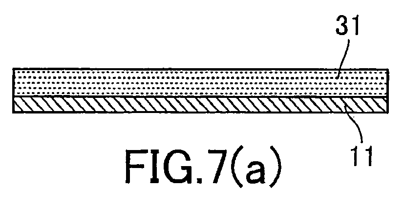
- FIG. 7(a) to 7(g) illustrate each step in the method of forming the partition 13 and the spacer 14 on the first substrate 11 in the electrophoretic display medium 10, as the first embodiment of the present invention.
- FIG. 7(a) illustrates a first resist application step according to the present invention
- FIG. 7(b) illustrates a first mask positioning step according to the present invention
- FIG. 7(c) illustrates a first exposure step according to the present invention
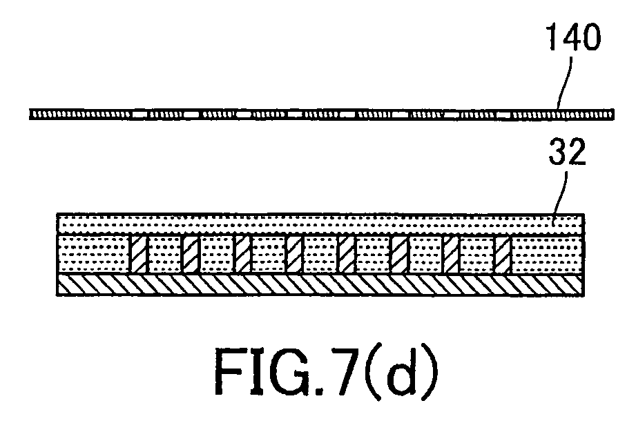
- FIG. 7(d) illustrates a second resist application step according to the present invention
- FIG. 7(e) illustrates a second mask positioning step according to the present invention
- FIG. 7(f) illustrates a second exposure step according to the present invention
- FIG. 7(g) illustrates a development step according to the present invention.
- a first negative resist 31 which is a negative-type resist made of a resin, a sensitizer, and a solvent, is applied on the first substrate 11.
- the first negative resist 31 is applied on the first substrate 11 at a thickness of 20 ⁇ m by the spin-coating method.
- the first negative resist 31 is then soft-baked so that the solvent in the first negative resist is driven off until the first negative resist 31 becomes not sticky.
- a first mask 140 is positioned over the first substrate 11 in a state that the first mask 140 is distant from the first negative resist 31.
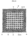
- FIG. 8 is an elevation view of the first mask 140.
- the first mask 140 is rectangular, having side portions 141 to 144.
- printing is made on a transparent glass plate with a light-shielding agent 145 (145A and 145B) so that a lattice-shaped aperture pattern 146 is formed thereon as shown in FIG. 8 .
- the aperture pattern 146 is a region in which no printing is made with the light-shielding agent on the transparent glass substrate.
- the light-shielding agent 145 includes a substantially square light-shielding part 145A, and a light-shielding part 145B printed along the side portions 141 to 144.
- Each side of the light-shielding part 145A is either parallel or orthogonal to the side portions 141 to 144.
- a plurality of the light-shielding parts 145A is provided at regular intervals along with the up-and-down and right-and-left directions.
- the light-shielding part 145B is printed along and in parallel with the side portions 141 to 144, covering from the side portions 141 to 144 toward the inward of the first mask 140 at a predetermined width.
- the first negative resist 31 is exposed to light through the above-mentioned first mask 140.
- the amount of the light exposure is equal to 500mJ/cm 2 .
- a post exposure bake is performed on the first negative resist 31.
- a latent image 63 having the same shape as the partition 13 is then formed.
- the latent image 63 contains a high proportion of solvent. The solvent is further driven off by post bake (to be described later), thereby completing the partition 13.
- a second negative resist 32 which is a negative-type resist, is applied on the first negative resist 31.
- the second negative resist 32 is applied on the first negative resist 31 at a thickness of 5 ⁇ m by the spin-coating method.
- the second negative resist 32 applied on the first negative resist 31 is then soft-baked until the second negative resist 32 becomes not sticky.
- the first mask 140 is removed from the first substrate 11.
- a second mask 150 is positioned over the first substrate 11 in a state that the second mask 150 is distant from the second negative resist 32.
- FIG. 9 is an elevation view of the second mask 150.
- the second mask 150 is rectangular, having side portions 151 to 154.
- printing is made on a transparent glass plate with a light-shielding agent 155 (155A, 155B) so that an aperture pattern 156 is formed thereon as shown in FIG. 9 .
- the aperture pattern 156 is a region in which no printing is made with the light-shielding agent on the transparent glass substrate.
- the light-shielding agent 155 includes a substantially square light-shielding part 155B, and a light-shielding part 155A printed along the side portions 151 to 154.
- Each side of the light-shielding part 155B is parallel or orthogonal to the side portions 151 to 154.
- the light-shielding part 155A is printed along and in parallel with the side portions 151 to 154, ranging from the side portions 151 to 154 toward the center of the second mask 150 at a predetermined width.
- the second negative resist 32 and the first negative resist 31 are exposed to light through the above-mentioned second mask 150.
- the amount of the light exposure is equal to 750mJ/cm 2 .
- a post exposure bake (PEB) is then performed on the second negative resist 32 and the first negative resist 31 so that a latent image 64 having the same shape as the spacer 14 is formed.
- a development is performed, with a developer, on the first negative resist 31 and the second negative resist 32, where the latent image 63 and the latent image 64 have been formed, so that a non-solidified portion (non-exposed portion) is removed.
- the latent image 63 and the latent image 64 left on the first substrate 11 are sintered by post bake, thereby forming the partition 13 and the spacer 14 on the first substrate 11.
- the partition 13 and the spacer 14 are formed integrally on the first substrate 11 by photo lithography, thereby allowing the partition 13 and the spacer 14 of different heights to be formed accurately.
- the amount of the light exposure 750mJ/cm 2 in the second exposure step is greater than the amount of the light exposure 500mJ/cm 2 in the first exposure step. Therefore, the latent image 64 is formed on the layers of the second and first negative resists without failure. Specifically, an adjustment of the amount of the light exposure is made by making the exposure duration longer in the second exposure step than in the first exposure step, with the same light source. In this case, the amount of the light exposure 500mJ/cm 2 is required for solidifying a negative resist of 20 ⁇ m thickness, and the amount of the light exposure 750mJ/cm 2 is required for solidifying a negative resist of 25 ⁇ m thickness.
- the amount of the light exposure in the first exposure step may be greater than 500mJ/cm 2 , an amount of the light exposure could be performed at 750mJ/cm 2 in the first exposure step and at 750mJ/cm 2 in the second exposure step.
- FIG. 10(a) to 10(g) illustrate each step in the method of forming the partition 13 and the spacer 14 on the first substrate 11 in the electrophoretic display medium 10, as the second embodiment of the present invention.
- FIG. 10(a) illustrates a first resist application step according to the present invention
- FIG. 10(b) illustrates a first mask positioning step according to the present invention
- FIG. 10(c) illustrates a first exposure step according to the present invention
- FIG. 10(d) illustrates a second resist application step according to the present invention
- FIG. 10(e) illustrates a second mask positioning step according to the present invention
- FIG. 10(f) illustrates a second exposure step according to the present invention
- FIG. 10(g) illustrates a development step according to the present invention.
- the first negative resist 31 is applied on the first substrate 11 at a thickness of 20 ⁇ m by the spin-coating method.
- the first negative resist 31 applied on the first substrate 11 is then soft-baked until the first negative resist 31 becomes not sticky.
- a first mask 170 is positioned over the first substrate 11 in a state that the first mask 170 is distant from the first negative resist 31.
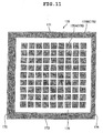
- FIG. 11 is an elevation view of the first mask 170.
- printing is made on a glass plate with a light-shielding agent 175 (175A and 175B) so that an aperture pattern 176 is formed thereon.
- the aperture pattern 176 has a shape obtained by combining the lattice-shaped aperture pattern 146 formed on the first mask 140 according to the first embodiment, and the rectangular aperture pattern 156 formed on the second mask 150 according to the first embodiment.
- each of the light-shielding agents 145A disposed in the top and bottom rows as well as in the leftmost and rightmost columns are in contact with the light-shielding agent 145B.
- each of the light-shielding agents 175A disposed in the top and bottom rows as well as in the leftmost and rightmost columns is printed so as to keep a predetermined distance from the light-shielding agent 175B.
- the first negative resist 31 is exposed to light through the above-mentioned first mask 170.
- the amount of the light exposure is equal to 500mJ/cm 2 .
- a post exposure bake (PEB) is then performed on the first negative resist 31 so that a latent image 63 having the same shape as the partition 13 is formed.
- the aperture pattern 176 on the first mask 170 according to the second embodiment has a shape obtained from the combination of the lattice-shaped aperture pattern 146 formed on the first mask 140 according to the first embodiment, and the rectangular aperture pattern 156 formed on the second mask 150 according to the first embodiment. Therefore, a latent image 64a, which is a part of the latent image 64, having the same shape as the spacer, is also formed in the first negative resist 31.
- a second negative resist 32 which is a negative-type resist, is applied on the first negative resist 31.
- the second negative resist 32 is applied on the first negative resist 31 at a thickness of 5 ⁇ m by the spin-coating method.
- the second negative resist 32 applied on the first negative resist 31 is then soft-baked until the second negative resist 32 becomes not sticky.
- a second mask 180 is positioned over the first mask 170 so that the second mask 180 is positioned over the first substrate 11.
- FIG. 12 is an elevation view of the second mask 180.
- printing is made on a glass plate with a light-shielding agent 185 (185A and 185B) so that a rectangular aperture pattern 186 is formed thereon as shown in FIG. 12 .
- the second negative resist 32 is exposed to light through the above-mentioned second mask 180 and the first mask 170.
- a post exposure bake (PEB) is then performed on the second negative resist 32 so that the remainder of the latent image 64 is formed on the top surface of the latent image 64a. Therefore, similarly to the first embodiment, the latent image 64 having the same shape as the spacer 14 is formed on the first substrate 11.
- a development is performed, with a developer, on the first negative resist 31 and the second negative resist 32, where the latent image 63 and the latent image 64 are formed.
- the latent image 63 and the latent image 64 left on the first substrate 11 are sintered by post bake, thereby forming the partition 13 and the spacer 14 on the first substrate 11.
- the partition and the spacer can be formed efficiently.
- the average diameter of the charged particles 15 is 3 ⁇ m
- the partition 13 is 20 ⁇ m high
- the spacer 14 is 25 ⁇ m high.
- the present invention is not limited to these values.
- neither the first substrate 11 nor the second substrate 12 of the electrophoretic display medium 10 directly includes an electrode for applying an electric field to the charged particles 15.
- the first substrate 11 and the second substrate 12 may include electrodes directly. If this is the case, as electrodes formed on the first substrate 11 and the second substrate 12, well-known electrodes, including a TFT electrode and a simple-matrix type electrode, may be employed.
- the above embodiments relate to the case in which the dispersion medium 16 has black charged particles 15 dispersed therein, but the color of the charged particles 15 dispersed in the dispersion medium 16 is not limited to black.
- the dispersion medium 16 having black charged particles 15 dispersed therein is dyed in white, but the dispersion medium 16 can be transparent, wherein white charged particles having the polarity opposite to the charged particles 15 are dispersed.
- the spacer 14 is formed only in the outer regions of the first substrate 11 and the second substrate 12, but a part of the partition can be formed so as to be in contact with the second substrate 12 and thus used as a spacer for defining the distance between the first substrate 11 and the second substrate 12.
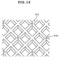
- FIG. 13 and FIG. 14 are perspective views showing a partition 313 formed so that a part of the partition works as a spacer. In FIG.
- a lattice-shaped partition includes a lower partition 313a and a higher partition 313b.
- a plurality of columns 313c is provided on the partition 313 at a designated interval.
- the partition is not limited to a specific shape. Also in the above embodiments, while the partition is formed like a lattice shape as viewed from the first substrate side, it is also possible for the partition to have other shapes, such as polygons like a honeycomb, parallel lines or waves.
- the second mask 180 is positioned over the first mask 170 without removing the first mask 170 in the second mask positioning step.
- the second substrate 12 is formed of transparent polyethylene terephthalate, thus the top surface of the second substrate 12 being used as a display region in the electrophoretic display medium 10.
- the first substrate 11 can be formed of transparent polyethylene terephthalate so that a surface of the first substrate 11 is employed as a display region.
- a liquid resist is employed in the first resist application step and the second resist application step, but the present invention is not limited to this type.
- a dry-film type resist may be applied.
Landscapes
- Physics & Mathematics (AREA)
- Nonlinear Science (AREA)
- General Physics & Mathematics (AREA)
- Optics & Photonics (AREA)
- Health & Medical Sciences (AREA)
- Life Sciences & Earth Sciences (AREA)
- Chemical & Material Sciences (AREA)
- Chemical Kinetics & Catalysis (AREA)
- Electrochemistry (AREA)
- Molecular Biology (AREA)
- Electrochromic Elements, Electrophoresis, Or Variable Reflection Or Absorption Elements (AREA)
Abstract




Description
- The present invention relates to an electrophoretic display medium, and a method of forming a partition and a spacer on a first substrate in the electrophoretic display medium.
- A conventional electrophoretic display medium well known in the art is provided with a dispersion medium injected between pair of substrates with positive or negative charged particles dispersed therein so as to display an image. In such an electrophoretic display medium, a pair of substrates is disposed to face each other. With the application of an electric field, charged particles migrate between the substrates, thereby displaying an image.
- There provided in such an electrophoretic display medium are a partition that partitions the region between the substrates, and a spacer disposed on the outer circumference of a substrate for defining the distance between the substrates.
- Patent document 1 discloses such an electrophoretic display medium in which a spacer and a partition are disposed between substrates. Patent Document 1: Japanese Utility Model Application Publication No.
S56-108171 - In order to manufacture such an electrophoretic display medium having a partition and a spacer, following methods are available. One method is to form a spacer on an outer circumference of a substrate, followed by forming a partition in a region inside the spacer formed on the outer circumference. The other method is to form a partition on a substrate, followed by forming a spacer on an outer circumference of the substrate so as to enclose the partition. In these methods, an adhesive is applied between the partition and the substrate so that the partition and the substrate are fixed together persistently. In order to fix the spacer and the substrate together persistently, an adhesive is also applied between the spacer and the substrate.
- However, in such an electrophoretic display medium, if there is a demand that the partition be lower than the spacer, it is difficult to make a level difference between the partition and the spacer accurately in the above method where the partition and the spacer formed separately are mounted on the substrate. This is because of the difficulty in having an accurate control over the adhesive thickness between the partition and the substrate as well as between the spacer and the substrate.
- The present invention is made to solve the above problem, and it is an object of the present invention to provide a method of allowing a partition and a spacer of different heights to be formed on a substrate accurately, and an electrophoretic display medium where a partition and a spacer of different heights are formed accurately.
- In order to achieve this object, claim 1 discloses a method for of forming a partition and a spacer on a first substrate in an electrophoretic display medium. The electrophoretic display medium includes a first substrate and a second substrate facing each other, a dispersion medium injected between the first substrate and the second substrate with charged particles dispersed therein, a partition for partitioning a region between the first substrate and the second substrates, and a spacer disposed between the first substrate and the second substrate for defining a distance therebetween. The method includes a first resist application step for applying a first negative resist on the first substrate, a first exposure step for exposing the first negative resist to light through a first mask having an aperture pattern through which a pattern of the partition is exposed to light after the first resist application step, a second resist application step for applying a second negative resist on the first negative resist after the first exposure step, a second exposure step for exposing the second negative resist and the first negative resist to light through a second mask having an aperture pattern through which a pattern of the spacer is exposed to light after the second resist application step, and a development step for developing the first negative resist and the second negative resist after the second exposure step.
- Another method of forming a partition and a spacer on the first substrate in an electrophoretic display medium disclosed in claim 2 is characterized in that an amount of the light exposure in the second exposure step is greater than an amount of the light exposure in the first step.
- Claim 3 discloses further method of forming a partition and a spacer on a first substrate in an electrophoretic display medium which includes a first substrate and a second substrate facing each other, a dispersion medium injected between the first substrate and the second substrate with charged particles dispersed therein, a partition for partitioning a region between the first and the second substrates, and a spacer disposed between the first substrate and the second substrate for defining a distance therebetween. The method includes a first resist application step for applying a first negative resist on the first substrate, a first exposure step for exposing the first negative resist to light through a first mask having an aperture pattern through which patterns of the partition and the spacer are exposed to light after the first resist application step, a second resist application step for applying a second negative resist on the first negative resist after the first exposure step, a second exposure step for exposing the second negative resist to light through a second mask having an aperture pattern through which a pattern of the spacer is exposed to light after the second resist application step, and a development step for developing the first negative resist and the second negative resist after the second exposure step.
- Another method of forming a partition and a spacer on a first substrate in an electrophoretic display medium disclosed in claim 4 further includes the following steps in addition to the steps disclosed in claim 3, that is, a first mask positioning step for positioning the first mask over the first substrate in a state that the first mask is distant from the first negative resist before the first exposure step, and a second mask positioning step for positioning a second mask over the first substrate without removing the first mask from the first substrate before the second exposure step.
- Further, claim 5 discloses another method of forming a partition and a spacer on a first substrate in an electrophoretic display medium wherein following steps may be executed in the methods disclosed in any one of claims 1 thorough 3. That is, a first mask positioning step for positioning the first mask over the first substrate before the first exposure step, and a second mask positioning step for positioning the second mask over the first substrate after removing the first mask from the first substrate before the second exposure step.
- Claim 6 describes an electrophoretic display medium that includes a first substrate and a second substrate facing each other, a dispersion medium injected between the first substrate and the second substrate with charged particles dispersed therein, a partition for partitioning a region between the first and the second substrates, and a spacer disposed between the first substrate and the second substrate for defining a distance therebetween. The partition and the spacer of this electrophoretic display medium are formed on the first substrate by a method including a first resist application step for applying a first negative resist on the first substrate, a first exposure step for exposing the first negative resist to light through a first mask having an aperture pattern through which a pattern of the partition is exposed to light after the first resist application step, a second resist application step for applying a second negative resist on the first negative resist after the first exposure step, a second exposure step for exposing the second negative resist and the first negative resist to light through a second mask having an aperture pattern through which a pattern of the spacer is exposed to light after the second resist application step, and a development step for developing the first negative resist and the second negative resist after the second exposure step.
- Further, claim 7 discloses an electrophoretic display medium which includes a first substrate and a second substrate facing each other, a dispersion medium injected between the first substrate and the second substrate with charged particles dispersed therein, a partition for partitioning a region between the first and the second substrates, and a spacer disposed between the first substrate and the second substrate for defining a distance therebetween. The partition and the spacer of this electrophoretic display medium are manufactured according to a method wherein included are a first resist application step for applying a first negative resist on the first substrate, a first exposure step for exposing the first negative resist to light through a first mask having an aperture pattern through which patterns of the partition and the spacer are exposed to light after the first resist application step, a second resist application step for applying the second negative resist on the first negative resist after the first exposure step, a second exposure step for exposing the second negative resist to light through a second mask having an aperture pattern through which a pattern of the spacer is exposed to light after the second resist application step, and a development step for developing the first negative resist and the second negative resist after the second exposure step.
- According to the invention disclosed in claim 1, a partition and a spacer are formed integrally on a first substrate by photolithography, thereby allowing the partition and the spacer of different heights to be formed accurately.
- According to the invention disclosed in claim 2, in addition to the effect produced by the invention disclosed in claim 1, an amount of the light exposure in the second exposure step is greater than an amount of the light exposure in the first exposure step, thereby allowing the spacer to be formed without failure.
- According to the invention disclosed in claim 3, a partition and a spacer are formed integrally on a first substrate by photolithography, thereby allowing the partition and the spacer of different heights to be formed accurately.
- According to the invention disclosed in claim 4, in addition to the effect produced by the invention disclosed in claim 3, a first mask does not have to be removed in a second mask positioning step, thereby allowing the partition and the spacer to be formed efficiently.
- According to the invention disclosed in claim 5, in addition to the effect produced by the invention disclosed in any one of claims 1 through 3, the second mask is positioned after removing the first mask in the second mask positioning step, thereby allowing the partition and the spacer to be formed without failure.
- According to the invention disclosed in claim 6, since a partition and a spacer are formed integrally on a first substrate by photolithography, the partition and the spacer of different heights are formed accurately.
- According to the invention disclosed in claim 7, since a partition and a spacer are formed integrally on a first substrate by photolithography, the partition and the spacer of different heights are formed accurately.
-
-
FIG. 1 is a perspective view showing the appearance of an electrophoretic display medium. -
FIG. 2 illustrates the internal configuration of the electrophoretic display medium. -
FIG. 3 is a perspective view showing a partition and a spacer. -
FIG. 4 shows the electrophoretic display medium in a state that black color is displayed across a display region. -
FIG. 5 shows the electrophoretic display medium in a state that white color is displayed across a display region. -
FIG. 6 illustrates an electrophoretic display medium having a partition whose top face is in contact with an underside portion of a second substrate. -
FIG. 7(a) to 7(g) illustrate each step in the method of forming the partition and the spacer of the electrophoretic display medium on a first substrate, as a first embodiment of the present invention. -
FIG. 8 is an elevation view showing a first mask. -
FIG. 9 is an elevation view showing a second mask. -
FIG. 10(a) to 10(g) illustrate each step in the method of forming the partition and the spacer of the electrophoretic display medium on the first substrate, as a second embodiment. -
FIG. 11 is an elevation view showing a first mask. -
FIG. 12 is an elevation view showing a second mask. -
FIG. 13 is a perspective view showing one example of a partition formed so that part of the partition works also as a spacer. -
FIG. 14 is a perspective view showing one example of a partition formed so that part of the partition works also as a spacer. -
- 10 electrophoretic display medium
- 11 first substrate
- 12 second substrate
- 13 partition
- 14 spacer
- 15 charged particles
- 16 dispersion medium
- 31 first negative resist
- 32 second negative resist
- 140, 170 first mask
- 146, 176 aperture pattern
- 145A, 145B, 175A, 175B light-shielding agent
- 150, 180 second mask
- 156, 186 aperture pattern
- 155A, 155B, 185A, 185B light-shielding agent
- Hereinafter, embodiments of the present invention will be described with reference to the accompanying drawings.
- First, a description is given for an
electrophoretic display medium 10 having apartition 13 and aspacer 14, formed in a method of forming a partition and a spacer of an electrophoretic display medium on a substrate, as the embodiments of the present invention. -
FIG. 1 is a perspective view showing the appearance of theelectrophoretic display medium 10. As shown inFIG. 1 , in theelectrophoretic display medium 10, provided are afirst substrate 11 formed of polyethylene terephthalate (PET) into a rectangular shape, and asecond substrate 12 formed of polyethylene terephthalate into a rectangular shape in the same manner, so as to face each other. Note that thesecond substrate 12 is formed of transparent polyethylene terephthalate; the top face of thesecond substrate 12 is designed to display an image. In theelectrophoretic display medium 10, the top face of thesecond substrate 12 corresponds to a display surface. A display region 1, which is a central portion of the display surface of thesecond substrate 12, displays an image. - A
spacer 14 is formed on the outer circumference of the region confined between thefirst substrate 11 and thesecond substrate 12. Thespacer 14 defines the distance between thefirst substrate 11 and thesecond substrate 12. Thespacer 14 also seals and prevents adispersion medium 16 and charged particles 15 (to be described later) injected between thefirst substrate 11 and thesecond substrate 12 from leaking to outside. - A description is given for the internal configuration of the
electrophoretic display medium 10 with reference toFIG. 2. FIG. 2 illustrates the internal configuration of theelectrophoretic display medium 10. As shown inFIG. 2 , injected between thefirst substrate 11 and thesecond substrate 12 is thedispersion medium 16 wherein black chargedparticles 15 having a negative polarity are dispersed. Thedispersion medium 16 is dyed in white. The average diameter of the chargedparticles 15 is 3µm. - The
partition 13 formed in the method according to the present invention is provided on thefirst substrate 11. Thepartition 13 is formed so as to prevent the chargedparticles 15 from traveling in a horizontal direction. This means that thepartition 13 prevents uneven distribution of the chargedparticles 15 between thefirst substrate 11 and thesecond substrate 12 relative to a horizontal direction. The chargedparticles 15, therefore, are provided at an even density in a horizontal direction. Now that uneven distribution of the chargedparticles 15 is prevented between the substrates, the chargedparticles 15 are dispersed evenly between the substrates relative to a horizontal direction, thereby preventing unevenness from appearing on a displayed image. -
FIG. 3 is a perspective view showing thepartition 13 and thespacer 14. Thepartition 13 and thespacer 14 are integrally formed of epoxy resin in a method to be described later. Thepartition 13 is formed like a grid pattern when viewed from above. Thespacer 14 has a rectangular shape so as to enclose the grid-like partition 13. - As will be described later, since the height of the
partition 13 is formed lower than the height of thespacer 14, the top face of thepartition 13 does not make contact with thesecond substrate 12. Specifically, thepartition 13 is 20µm high, and thespacer 14 is 25µm high. This means that a gap of 5µm is left between the upper surface of thepartition 13 and the undersurface of thesecond substrate 12. - Next, a description is given for display switching operation in the
electrophoretic display medium 10. In theelectrophoretic display medium 10, neither thefirst substrate 11 nor thesecond substrate 12 directly includes an electrode for applying an electric field to the chargedparticles 15. Accordingly, in order to perform a display switching operation, as shown inFIG. 4 ,electrodes 21 andelectrodes 22 are externally arranged so as to apply an electric field to the charged particles between the substrates. Theelectrodes 21 are arranged on thefirst substrate 11 side, while theelectrodes 22 are arranged on thesecond substrate 12 side. In order to make the description simpler, in this case, the assumption is made that a pair ofelectrode 21 andelectrode 22 is provided for each pixel. Accordingly, a voltage applied to the pair ofelectrode 21 andelectrode 22 is controlled so that display switching is controlled for each pixel. -
FIG. 4 shows a state that the black color is displayed across the display region 1 shown inFIG. 1 . In this case, a voltage of 0V is applied to all theelectrodes 21, and a voltage of 50V is applied to all theelectrodes 22. As a consequence, the negatively chargedparticles 15 migrate to thesecond substrate 12 side. The black chargedparticles 15 are then adhered to thesecond substrate 12. The black color is thus displayed across the display region 1. - In the case described above, a voltage is applied to both of the
electrodes 21 and theelectrodes 22 in order to move the chargedparticles 15. Further, even when the voltages applied to both electrodes could drop down to 0V, the state that the chargedparticles 15 are being adhered to thesecond substrate 12 is maintained. -
FIG. 5 shows a state that the white color is displayed across the display region 1. In this case, a voltage of 50V is applied to all theelectrodes 21, and a voltage of 0V is applied to all theelectrodes 22. The negatively chargedparticles 15 migrate to thefirst substrate 11 side. The black chargedparticles 15 are then adhered to thefirst substrate 11, thereby leaving only thewhite dispersion medium 16 on thesecond substrate 12 side. The white color is thus displayed across the display region 1. - As has been described above, a gap of 5µm is left between the upper surface of the
partition 13 and the undersurface of thesecond substrate 12. The average diameter of the chargedparticles 15 is 3µm. Therefore, as shown inFIG. 4 , when the black color is displayed across the display region 1, the chargedparticles 15 can penetrate into the gap between the upper surface of thepartition 13 and the undersurface of thesecond substrate 12. The black color is thus displayed across the display region 1. - On the other hand, as shown in
FIG. 6 , in anelectrophoretic display medium 200 having apartition 213 whose top surface is in contact with the undersurface of thesecond substrate 12, there is no gap left between the upper surface of thepartition 213 and the undersurface of thesecond substrate 12. The display region 1, therefore, necessarily has to have an area where the black color cannot be displayed. - As has been described above, by forming the height of the
partition 13 lower than the height of thespacer 14, the display region 1 is effectively utilized in theelectrophoretic display medium 10. - Next, a description is given for a method of forming the
partition 13 and thespacer 14 on thefirst substrate 11 in theelectrophoretic display medium 10, as a first embodiment of the present invention. -
FIG. 7(a) to 7(g) illustrate each step in the method of forming thepartition 13 and thespacer 14 on thefirst substrate 11 in theelectrophoretic display medium 10, as the first embodiment of the present invention.FIG. 7(a) illustrates a first resist application step according to the present invention;FIG. 7(b) illustrates a first mask positioning step according to the present invention;FIG. 7(c) illustrates a first exposure step according to the present invention;FIG. 7(d) illustrates a second resist application step according to the present invention;FIG. 7(e) illustrates a second mask positioning step according to the present invention;FIG. 7(f) illustrates a second exposure step according to the present invention; andFIG. 7(g) illustrates a development step according to the present invention. - First, referring to
FIG. 7(a) , in the first resist application step, a first negative resist 31, which is a negative-type resist made of a resin, a sensitizer, and a solvent, is applied on thefirst substrate 11. The first negative resist 31 is applied on thefirst substrate 11 at a thickness of 20µm by the spin-coating method. The first negative resist 31 is then soft-baked so that the solvent in the first negative resist is driven off until the first negative resist 31 becomes not sticky. - Next, referring to
FIG. 7(b) , in the first mask positioning step, afirst mask 140 is positioned over thefirst substrate 11 in a state that thefirst mask 140 is distant from the first negative resist 31. - Here, a description is given for the
first mask 140 with reference toFIG. 8. FIG. 8 is an elevation view of thefirst mask 140. Thefirst mask 140 is rectangular, havingside portions 141 to 144. For thefirst mask 140, printing is made on a transparent glass plate with a light-shielding agent 145 (145A and 145B) so that a lattice-shapedaperture pattern 146 is formed thereon as shown inFIG. 8 . Specifically, theaperture pattern 146 is a region in which no printing is made with the light-shielding agent on the transparent glass substrate. More specifically, the light-shieldingagent 145 includes a substantially square light-shieldingpart 145A, and a light-shieldingpart 145B printed along theside portions 141 to 144. Each side of the light-shieldingpart 145A is either parallel or orthogonal to theside portions 141 to 144. A plurality of the light-shieldingparts 145A is provided at regular intervals along with the up-and-down and right-and-left directions. The light-shieldingpart 145B is printed along and in parallel with theside portions 141 to 144, covering from theside portions 141 to 144 toward the inward of thefirst mask 140 at a predetermined width. - Next, referring to
FIG. 7(c) , in the first exposure step, the first negative resist 31 is exposed to light through the above-mentionedfirst mask 140. This solidifies the resin of the portion exposed to light in the first negative resist because of the action of the sensitizer. In this case, the amount of the light exposure is equal to 500mJ/cm2. In order to smooth the sides of the portion solidified by exposure, a post exposure bake (PEB) is performed on the first negative resist 31. Alatent image 63 having the same shape as thepartition 13 is then formed. Thelatent image 63 contains a high proportion of solvent. The solvent is further driven off by post bake (to be described later), thereby completing thepartition 13. - Next, referring to
FIG. 7(d) , in the second resist application step, a second negative resist 32, which is a negative-type resist, is applied on the first negative resist 31. The second negative resist 32 is applied on the first negative resist 31 at a thickness of 5µm by the spin-coating method. The second negative resist 32 applied on the first negative resist 31 is then soft-baked until the second negative resist 32 becomes not sticky. - Next, referring to
FIG. 7(e) , in the second mask positioning step, thefirst mask 140 is removed from thefirst substrate 11. Asecond mask 150 is positioned over thefirst substrate 11 in a state that thesecond mask 150 is distant from the second negative resist 32. - Here, a description is given for the
second mask 150 with reference toFIG. 9. FIG. 9 is an elevation view of thesecond mask 150. Thesecond mask 150 is rectangular, havingside portions 151 to 154. For thesecond mask 150, printing is made on a transparent glass plate with a light-shielding agent 155 (155A, 155B) so that anaperture pattern 156 is formed thereon as shown inFIG. 9 . Specifically, theaperture pattern 156 is a region in which no printing is made with the light-shielding agent on the transparent glass substrate. More specifically, the light-shieldingagent 155 includes a substantially square light-shieldingpart 155B, and a light-shieldingpart 155A printed along theside portions 151 to 154. Each side of the light-shieldingpart 155B is parallel or orthogonal to theside portions 151 to 154. The light-shieldingpart 155A is printed along and in parallel with theside portions 151 to 154, ranging from theside portions 151 to 154 toward the center of thesecond mask 150 at a predetermined width. - Next, referring to
FIG. 7(f) in the second exposure step, the second negative resist 32 and the first negative resist 31 are exposed to light through the above-mentionedsecond mask 150. In this case, the amount of the light exposure is equal to 750mJ/cm2. A post exposure bake (PEB) is then performed on the second negative resist 32 and the first negative resist 31 so that alatent image 64 having the same shape as thespacer 14 is formed. - Next, referring to
FIG. 7(g) , in the development step, a development is performed, with a developer, on the first negative resist 31 and the second negative resist 32, where thelatent image 63 and thelatent image 64 have been formed, so that a non-solidified portion (non-exposed portion) is removed. After that, thelatent image 63 and thelatent image 64 left on thefirst substrate 11 are sintered by post bake, thereby forming thepartition 13 and thespacer 14 on thefirst substrate 11. - According to the first embodiment, the
partition 13 and thespacer 14 are formed integrally on thefirst substrate 11 by photo lithography, thereby allowing thepartition 13 and thespacer 14 of different heights to be formed accurately. - According to the first embodiment, the amount of the light exposure 750mJ/cm2 in the second exposure step is greater than the amount of the light exposure 500mJ/cm2 in the first exposure step. Therefore, the
latent image 64 is formed on the layers of the second and first negative resists without failure. Specifically, an adjustment of the amount of the light exposure is made by making the exposure duration longer in the second exposure step than in the first exposure step, with the same light source. In this case, the amount of the light exposure 500mJ/cm2 is required for solidifying a negative resist of 20µm thickness, and the amount of the light exposure 750mJ/cm2 is required for solidifying a negative resist of 25µm thickness. Therefore, since the amount of the light exposure in the first exposure step may be greater than 500mJ/cm2, an amount of the light exposure could be performed at 750mJ/cm2 in the first exposure step and at 750mJ/cm2 in the second exposure step. - Next, a description is given for a method of forming the
partition 13 and thespacer 14 on thefirst substrate 11 in theelectrophoretic display medium 10, as a second embodiment of the present invention. -
FIG. 10(a) to 10(g) illustrate each step in the method of forming thepartition 13 and thespacer 14 on thefirst substrate 11 in theelectrophoretic display medium 10, as the second embodiment of the present invention.FIG. 10(a) illustrates a first resist application step according to the present invention;FIG. 10(b) illustrates a first mask positioning step according to the present invention;FIG. 10(c) illustrates a first exposure step according to the present invention;FIG. 10(d) illustrates a second resist application step according to the present invention;FIG. 10(e) illustrates a second mask positioning step according to the present invention;FIG. 10(f) illustrates a second exposure step according to the present invention; andFIG. 10(g) illustrates a development step according to the present invention. - First, referring to
FIG. 10(a) , in the first resist application step, a first negative resist 31, which is a negative-type resist, is applied on thefirst substrate 11. The first negative resist 31 is applied on thefirst substrate 11 at a thickness of 20µm by the spin-coating method. The first negative resist 31 applied on thefirst substrate 11 is then soft-baked until the first negative resist 31 becomes not sticky. - Next, referring to
FIG. 10(b) , in the first mask positioning step, afirst mask 170 is positioned over thefirst substrate 11 in a state that thefirst mask 170 is distant from the first negative resist 31. - Here, a description is given for the
first mask 170 with reference toFIG. 11. FIG. 11 is an elevation view of thefirst mask 170. As shown inFIG. 11 , for thefirst mask 170, printing is made on a glass plate with a light-shielding agent 175 (175A and 175B) so that anaperture pattern 176 is formed thereon. Theaperture pattern 176 has a shape obtained by combining the lattice-shapedaperture pattern 146 formed on thefirst mask 140 according to the first embodiment, and therectangular aperture pattern 156 formed on thesecond mask 150 according to the first embodiment. In thefirst mask 140 according to the first embodiment, among a plurality of light-shieldingagents 145A, each of the light-shieldingagents 145A disposed in the top and bottom rows as well as in the leftmost and rightmost columns are in contact with the light-shieldingagent 145B. In the second embodiment, however, each of the light-shieldingagents 175A disposed in the top and bottom rows as well as in the leftmost and rightmost columns is printed so as to keep a predetermined distance from the light-shieldingagent 175B. - Next, referring to
FIG. 10(c) , in the first exposure step, the first negative resist 31 is exposed to light through the above-mentionedfirst mask 170. In this case, the amount of the light exposure is equal to 500mJ/cm2. A post exposure bake (PEB) is then performed on the first negative resist 31 so that alatent image 63 having the same shape as thepartition 13 is formed. In this case, as mentioned above, theaperture pattern 176 on thefirst mask 170 according to the second embodiment has a shape obtained from the combination of the lattice-shapedaperture pattern 146 formed on thefirst mask 140 according to the first embodiment, and therectangular aperture pattern 156 formed on thesecond mask 150 according to the first embodiment. Therefore, alatent image 64a, which is a part of thelatent image 64, having the same shape as the spacer, is also formed in the first negative resist 31. - Next, referring to
FIG. 10(d) , in the second resist application step, a second negative resist 32, which is a negative-type resist, is applied on the first negative resist 31. The second negative resist 32 is applied on the first negative resist 31 at a thickness of 5µm by the spin-coating method. The second negative resist 32 applied on the first negative resist 31 is then soft-baked until the second negative resist 32 becomes not sticky. - Next, referring to
FIG. 10(e) , in the second mask positioning step, without removing thefirst mask 170 from thefirst substrate 11, asecond mask 180 is positioned over thefirst mask 170 so that thesecond mask 180 is positioned over thefirst substrate 11. - Here, a description is given for the
second mask 180 with reference toFIG. 12. FIG. 12 is an elevation view of thesecond mask 180. Similarly to thesecond mask 150 according to the first embodiment, for thesecond mask 180, printing is made on a glass plate with a light-shielding agent 185 (185A and 185B) so that arectangular aperture pattern 186 is formed thereon as shown inFIG. 12 . - Next, referring to
FIG. 10(f) , in the second exposure step, the second negative resist 32 is exposed to light through the above-mentionedsecond mask 180 and thefirst mask 170. A post exposure bake (PEB) is then performed on the second negative resist 32 so that the remainder of thelatent image 64 is formed on the top surface of thelatent image 64a. Therefore, similarly to the first embodiment, thelatent image 64 having the same shape as thespacer 14 is formed on thefirst substrate 11. - Next, referring to
FIG. 10(g) , in the development step, a development is performed, with a developer, on the first negative resist 31 and the second negative resist 32, where thelatent image 63 and thelatent image 64 are formed. After that, thelatent image 63 and thelatent image 64 left on thefirst substrate 11 are sintered by post bake, thereby forming thepartition 13 and thespacer 14 on thefirst substrate 11. - According to the second embodiment, since the first mask does not have to be removed in the second mask positioning step, the partition and the spacer can be formed efficiently.
- Further, the methods of forming a partition and a spacer on a first substrate in an electrophoretic display medium of this invention, as well as an electrophoretic display medium manufactured according to the methods of forming a partition and a spacer on a first substrate in an electrophoretic display medium, are not confined to the embodiments described above, and it would be apparent to those skilled in the art that many modifications and variations may be made therein without departing from the spirit of the invention.
- In the above embodiments, the average diameter of the charged
particles 15 is 3µm, thepartition 13 is 20µm high, and thespacer 14 is 25µm high. However, the present invention is not limited to these values. - Further, in the above embodiments, neither the
first substrate 11 nor thesecond substrate 12 of theelectrophoretic display medium 10 directly includes an electrode for applying an electric field to the chargedparticles 15. However, thefirst substrate 11 and thesecond substrate 12 may include electrodes directly. If this is the case, as electrodes formed on thefirst substrate 11 and thesecond substrate 12, well-known electrodes, including a TFT electrode and a simple-matrix type electrode, may be employed. - Further, the above embodiments relate to the case in which the
dispersion medium 16 has black chargedparticles 15 dispersed therein, but the color of the chargedparticles 15 dispersed in thedispersion medium 16 is not limited to black. - Further, in the above embodiments, the
dispersion medium 16 having black chargedparticles 15 dispersed therein is dyed in white, but thedispersion medium 16 can be transparent, wherein white charged particles having the polarity opposite to the chargedparticles 15 are dispersed.
Further, in the above embodiments, thespacer 14 is formed only in the outer regions of thefirst substrate 11 and thesecond substrate 12, but a part of the partition can be formed so as to be in contact with thesecond substrate 12 and thus used as a spacer for defining the distance between thefirst substrate 11 and thesecond substrate 12.FIG. 13 andFIG. 14 are perspective views showing apartition 313 formed so that a part of the partition works as a spacer. InFIG. 13 , a lattice-shaped partition includes alower partition 313a and ahigher partition 313b. InFIG. 14 , a plurality ofcolumns 313c is provided on thepartition 313 at a designated interval. Thus, the partition is not limited to a specific shape. Also in the above embodiments, while the partition is formed like a lattice shape as viewed from the first substrate side, it is also possible for the partition to have other shapes, such as polygons like a honeycomb, parallel lines or waves. - Further, in the second embodiment, the
second mask 180 is positioned over thefirst mask 170 without removing thefirst mask 170 in the second mask positioning step. However, only thesecond mask 180 can be positioned over the substrate after removing thefirst mask 170 in the second mask positioning step. Also in the above-mentioned embodiments, thesecond substrate 12 is formed of transparent polyethylene terephthalate, thus the top surface of thesecond substrate 12 being used as a display region in theelectrophoretic display medium 10. However, thefirst substrate 11 can be formed of transparent polyethylene terephthalate so that a surface of thefirst substrate 11 is employed as a display region. - Further, in the above embodiments, a liquid resist is employed in the first resist application step and the second resist application step, but the present invention is not limited to this type. For example, a dry-film type resist may be applied.
Claims (7)
- A method of forming a partition (13) and a spacer (14) on a first substrate (11) in an electrophoretic display medium (10), the electrophoretic display medium (10) comprising:
a first substrate (11) and a second substrate (12) facing each other;
a dispersion medium (16) injected between the first substrate (11) and the second substrate (12) with charged particles (15) dispersed therein;
a partition (13) for partitioning a region between the first substrate and the second substrate; and
a spacer (14) disposed between the first substrate(11) and the second substrate (12) for defining a distance therebetween;
the method comprising:a first resist application step for applying a first negative resist (31) on the first substrate (11);a first exposure step for exposing the first negative resist (31) to light through a first mask (140) having an aperture pattern through which a pattern of the partition (13) is exposed to light, the first exposure step being executed after the first resist application step;a second resist application step for applying a second negative resist (32) on the first negative resist (31), the second resist application step being executed after the first exposure step;a second exposure step for exposing the second negative resist (32) and the first negative resist (31) to light through a second mask (150) having an aperture pattern through which a pattern of the spacer (14) is exposed to light, the second exposure step being executed after the second resist application step; anda development step for developing the first negative resist (31) and the second negative resist (32), the development step being executed after the second exposure step. - The method of forming a partition (13) and a spacer (14) on a first substrate (11) in an electrophoretic display medium (10) according to claim 1, wherein an amount of the light exposure in the second exposure step is greater than an amount of the light exposure in the first exposure step.
- A method of forming a partition (13) and a spacer (14) on a first substrate (11) in an electrophoretic display medium (10), the electrophoretic display medium (10) comprising:
a first substrate (11) and a second substrate (12) facing each other;
a dispersion medium (16) injected between the first substrate (11) and the second substrate (12) with charged particles (15) dispersed therein;
a partition (13) for partitioning a region between the first substrate (11) and the second substrate (12);
a spacer (14) disposed between the first substrate(11) and the second substrate (12) for defining a distance therebetween;
the method comprising:a first resist application step for applying a first negative resist (31) on the first substrate (11);a first exposure step for exposing the first negative resist (31) to light through a first mask (170) having an aperture pattern through which patterns of the partition (13) and the spacer (14) are exposed to light, the first exposure step being executed after the first resist application step;a second resist application step for applying a second negative resist (32) on the first negative resist (31), the second resist application step being executed after the first exposure step;a second exposure step for exposing the second negative resist (32) to light through a second mask (180) having an aperture pattern through which a pattern of the spacer (14) is exposed to light, the second exposure step being executed after the second resist application step; anda development step for developing the first negative resist (31) and the second negative resist (32), the development step being executed after the second exposure step. - The method of forming a partition (13) and a spacer (14) on a first substrate (11) in an electrophoretic display medium (10) according to claim 3, further comprising:a first mask positioning step for positioning the first mask (170) over the first substrate (11) in a state that the first mask (170) is distant from the first negative resist (31), the first mask positioning step being executed before the first exposure step; anda second mask positioning step for positioning a second mask (180) over the first substrate (11) without removing the first mask (170) from the first substrate (11), the second mask positioning step being executed before the second exposure step.
- The method of forming a partition (13) and a spacer (14) on a first substrate (11) in an electrophoretic display medium (10) according to any one of claims 1 through 3, further comprising:a first mask positioning step for positioning the first mask (170) over the first substrate (11), the first mask positioning step being executed before the first exposure step; anda second mask positioning step for positioning the second mask (180) over the first substrate (11) after removing the first mask (170) from the first substrate (11), the second mask positioning step being executed before the second exposure step.
- An electrophoretic display medium (10) comprising:a first substrate (11) and a second substrate (12) facing each other;a dispersion medium (16) injected between the first substrate (11) and the second substrate (12) with charged particles (15) dispersed therein;a partition (13) for partitioning a region between the first substrate (11) and the second substrate (12); anda spacer (14) disposed between the first substrate (11) and the second substrate (12) for defining a distance therebetween;
wherein the partition (13) and the spacer (14) are formed on the first substrate (11) by a method comprising:a first resist application step for applying a first negative resist (31) on the first substrate (11);a first exposure step for exposing the first negative resist (31) to light through a first mask (140) having an aperture pattern through which a pattern of the partition (13) is exposed to light, the first exposure step being executed after the first resist application step;a second resist application step for applying a second negative resist (32) on the first negative resist (31), the second resist application step being executed after the first exposure step;a second exposure step for exposing the second negative resist (32) and the first negative resist (31) to light through a second mask (150) having an aperture pattern through which a pattern of the spacer (14) is exposed to light, the second exposure step being executed after the second resist application step; anda development step for developing the first negative resist (31) and the second negative resist (32), the development step being executed after the second exposure step. - An electrophoretic:display medium (10) comprising:a first substrate (11) and a second substrate (12) facing each other;a dispersion medium (16) injected between the first substrate (11) and the second substrate (12) with charged particles (15) dispersed therein;a partition (13) for partitioning a region between the first substrate (11) and the second substrate (12); anda spacer (14) disposed between the first substrate (11) and the second substrate (12) for defining a distance therebetween;
wherein the partition (13) and the spacer (14) are formed on the first substrate (11) by a method comprising:a first resist application step for applying a first negative resist (31) on the first substrate (11);a first exposure step for exposing the first negative resist (31) to light through a first mask (170) having an aperture pattern through which patterns of the partition (13) and the spacer (14) are exposed to light, the first exposure step being executed after the first resist application step;a second resist application step for applying the second negative resist (32) on the first negative resist (31), the second resist application step being executed after the first exposure step;a second exposure step for exposing the second negative resist (32) to light through a second mask (180) having an aperture pattern through which a pattern of the spacer (14) is exposed to light, the second exposure step being executed after the second resist application step; and a development step for developing the first negative resist (31) and the second negative resist (32), the development step being executed after the second exposure step.
Applications Claiming Priority (2)
| Application Number | Priority Date | Filing Date | Title |
|---|---|---|---|
| JP2005273575A JP4682767B2 (en) | 2005-09-21 | 2005-09-21 | Forming method for forming partition and spacer of electrophoretic display medium on substrate, and electrophoretic display medium formed by forming method of partition and spacer forming partition and spacer of electrophoretic display medium on substrate |
| PCT/JP2006/316011 WO2007034637A1 (en) | 2005-09-21 | 2006-08-14 | Electrophoretic display medium and its formation method |
Publications (3)
| Publication Number | Publication Date |
|---|---|
| EP1939677A1 true EP1939677A1 (en) | 2008-07-02 |
| EP1939677A4 EP1939677A4 (en) | 2009-09-02 |
| EP1939677B1 EP1939677B1 (en) | 2010-06-09 |
Family
ID=37888691
Family Applications (1)
| Application Number | Title | Priority Date | Filing Date |
|---|---|---|---|
| EP06796401A Not-in-force EP1939677B1 (en) | 2005-09-21 | 2006-08-14 | Method of forming a partition and a spacer on a substrate of an electrophoretic display medium |
Country Status (5)
| Country | Link |
|---|---|
| US (1) | US7724418B2 (en) |
| EP (1) | EP1939677B1 (en) |
| JP (1) | JP4682767B2 (en) |
| DE (1) | DE602006014855D1 (en) |
| WO (1) | WO2007034637A1 (en) |
Cited By (2)
| Publication number | Priority date | Publication date | Assignee | Title |
|---|---|---|---|---|
| EP2293142A4 (en) * | 2008-05-28 | 2011-10-19 | Bridgestone Corp | Electronic paper |
| EP3543783A4 (en) * | 2018-01-19 | 2020-09-02 | Wuxi Vision Peak Technology Co., Ltd. | DISPLAY PLASMA MODULE OF A PATTERNED STRUCTURE AND MANUFACTURING PROCESS FOR IT |
Families Citing this family (14)
| Publication number | Priority date | Publication date | Assignee | Title |
|---|---|---|---|---|
| JP2010044385A (en) * | 2008-08-11 | 2010-02-25 | Samsung Electro-Mechanics Co Ltd | Electronic paper display device and method of manufacturing the same |
| SG181797A1 (en) * | 2009-12-18 | 2012-07-30 | Idenix Pharmaceuticals Inc | 5,5-fused arylene or heteroarylene hepatitis c virus inhibitors |
| KR20120077159A (en) * | 2010-12-30 | 2012-07-10 | 삼성전기주식회사 | Electronic paper display device and method of manufacturing the same |
| JP2013225065A (en) * | 2012-04-23 | 2013-10-31 | Seiko Epson Corp | Electrophoretic display device and electronic apparatus |
| JP6469656B2 (en) | 2013-05-22 | 2019-02-13 | クリアインク ディスプレイズ, インコーポレイテッドClearink Displays, Inc. | Method and apparatus for improved color filter saturation |
| US10705404B2 (en) | 2013-07-08 | 2020-07-07 | Concord (Hk) International Education Limited | TIR-modulated wide viewing angle display |
| EP3019911A4 (en) * | 2013-07-08 | 2017-06-28 | Clearink Displays, Inc. | Tir-modulated wide viewing angle display |
| CN103529600B (en) * | 2013-10-23 | 2016-01-06 | 京东方科技集团股份有限公司 | A kind of chock insulator matter and preparation method thereof, display |
| KR102202796B1 (en) * | 2014-09-30 | 2021-01-15 | 엘지디스플레이 주식회사 | Polariztion control unit and 2-dimensional and 3-dimensional image display device having the same |
| JP6688291B2 (en) | 2014-10-08 | 2020-04-28 | クリアインク ディスプレイズ, インコーポレイテッドClearink Displays, Inc. | Reflective display with color filters aligned |
| US10386691B2 (en) | 2015-06-24 | 2019-08-20 | CLEARink Display, Inc. | Method and apparatus for a dry particle totally internally reflective image display |
| US10386547B2 (en) | 2015-12-06 | 2019-08-20 | Clearink Displays, Inc. | Textured high refractive index surface for reflective image displays |
| US10261221B2 (en) | 2015-12-06 | 2019-04-16 | Clearink Displays, Inc. | Corner reflector reflective image display |
| US20220397801A1 (en) * | 2019-09-30 | 2022-12-15 | Lg Innotek Co., Ltd. | Light route control member and display having the same |
Family Cites Families (10)
| Publication number | Priority date | Publication date | Assignee | Title |
|---|---|---|---|---|
| JPS56108171U (en) | 1980-01-21 | 1981-08-22 | ||
| JP3359309B2 (en) | 1998-10-29 | 2002-12-24 | キヤノン株式会社 | Method for manufacturing binary diffractive optical element |
| CA2376130C (en) | 2000-04-04 | 2010-03-30 | Lintec Corporation | Device and method for measuring adhesive strength |
| JP4006925B2 (en) * | 2000-05-30 | 2007-11-14 | セイコーエプソン株式会社 | Method for manufacturing electrophoretic display device |
| JP3805180B2 (en) * | 2000-09-14 | 2006-08-02 | 株式会社東芝 | Display element |
| CN1273856C (en) * | 2000-12-14 | 2006-09-06 | 皇家菲利浦电子有限公司 | Liquid crystal display laminate and method of manufacturing such |
| JP2003241234A (en) * | 2001-12-13 | 2003-08-27 | Bridgestone Corp | Image display and image displaying method |
| JP4125537B2 (en) * | 2002-05-08 | 2008-07-30 | 日本合成化学工業株式会社 | Pattern formation method |
| TW589506B (en) * | 2003-08-28 | 2004-06-01 | Ind Tech Res Inst | The manufacturing method for an electrophoretic display |
| JP4359155B2 (en) * | 2004-02-03 | 2009-11-04 | 株式会社東芝 | Electrophoretic display device |
-
2005
- 2005-09-21 JP JP2005273575A patent/JP4682767B2/en not_active Expired - Fee Related
-
2006
- 2006-08-14 EP EP06796401A patent/EP1939677B1/en not_active Not-in-force
- 2006-08-14 WO PCT/JP2006/316011 patent/WO2007034637A1/en not_active Ceased
- 2006-08-14 DE DE602006014855T patent/DE602006014855D1/en active Active
-
2008
- 2008-03-11 US US12/046,331 patent/US7724418B2/en not_active Expired - Fee Related
Cited By (3)
| Publication number | Priority date | Publication date | Assignee | Title |
|---|---|---|---|---|
| EP2293142A4 (en) * | 2008-05-28 | 2011-10-19 | Bridgestone Corp | Electronic paper |
| EP3543783A4 (en) * | 2018-01-19 | 2020-09-02 | Wuxi Vision Peak Technology Co., Ltd. | DISPLAY PLASMA MODULE OF A PATTERNED STRUCTURE AND MANUFACTURING PROCESS FOR IT |
| US11657998B2 (en) | 2018-01-19 | 2023-05-23 | Wuxi Vision Peak Technology Co., Ltd. | Display plasma module with a patterned structure and manufacturing method thereof |
Also Published As
| Publication number | Publication date |
|---|---|
| WO2007034637A1 (en) | 2007-03-29 |
| US7724418B2 (en) | 2010-05-25 |
| JP2007086286A (en) | 2007-04-05 |
| EP1939677B1 (en) | 2010-06-09 |
| US20080218845A1 (en) | 2008-09-11 |
| EP1939677A4 (en) | 2009-09-02 |
| DE602006014855D1 (en) | 2010-07-22 |
| JP4682767B2 (en) | 2011-05-11 |
Similar Documents
| Publication | Publication Date | Title |
|---|---|---|
| US7724418B2 (en) | Electrophoretic display medium and method of forming the same | |
| KR100662780B1 (en) | Liquid crystal display with test pixel and method of manufacturing black matrix using same | |
| KR100488953B1 (en) | A method for forming post spacer of lcd device | |
| KR20020046172A (en) | Liquid crystal display device | |
| JPS59171930A (en) | Electrophoresis display element | |
| KR20010062751A (en) | Liquid crystal display apparatus and method for manufacturing same | |
| WO2021259247A1 (en) | Display substrate and manufacturing method therefor, panel, display device, and mask plate | |
| JP2004061539A (en) | Color filter for liquid crystal and method for manufacturing same | |
| CN105093806A (en) | Ultraviolet (UV) mask and exposure method thereof | |
| JP2009069224A (en) | RESIN THIN FILM AND ITS MANUFACTURING METHOD, AND LIQUID CRYSTAL COLOR FILTER AND ITS MANUFACTURING METHOD | |
| KR100911421B1 (en) | Color filter forming method using mold and liquid crystal display device manufacturing method including the same | |
| KR101430696B1 (en) | Electrophoresis display device and preparation method of the same | |
| JP5163016B2 (en) | Color filter manufacturing method and photomask | |
| JP4359155B2 (en) | Electrophoretic display device | |
| JP4099947B2 (en) | Liquid crystal display | |
| KR100513085B1 (en) | Method of panel fabrication for microencapsulated electrophoretic display driven by External Field | |
| JP2008170633A (en) | Method for manufacturing partition of electrophoretic display panel and electrophoretic display panel | |
| JP2021002033A (en) | Color filter substrate, liquid crystal display device, and method of manufacturing color filter substrate | |
| CN106802508B (en) | Color filter substrate and forming method thereof | |
| CN101395528A (en) | Liquid crystal display apparatus and process for manufacturing the same | |
| KR20120067107A (en) | Color filter substrate for in-plain switching mode liquid crystal display device and method of fabricating the same | |
| CN115877613B (en) | Display panel manufacturing method, display panel and display device | |
| KR100672649B1 (en) | Liquid crystal display | |
| JP2013242445A (en) | Liquid crystal display panel, liquid crystal display device, and method for manufacturing liquid crystal display panel | |
| KR100771358B1 (en) | Liquid crystal display device |
Legal Events
| Date | Code | Title | Description |
|---|---|---|---|
| PUAI | Public reference made under article 153(3) epc to a published international application that has entered the european phase |
Free format text: ORIGINAL CODE: 0009012 |
|
| 17P | Request for examination filed |
Effective date: 20080310 |
|
| AK | Designated contracting states |
Kind code of ref document: A1 Designated state(s): AT BE BG CH CY CZ DE DK EE ES FI FR GB GR HU IE IS IT LI LT LU LV MC NL PL PT RO SE SI SK TR |
|
| A4 | Supplementary search report drawn up and despatched |
Effective date: 20090731 |
|
| GRAP | Despatch of communication of intention to grant a patent |
Free format text: ORIGINAL CODE: EPIDOSNIGR1 |
|
| RTI1 | Title (correction) |
Free format text: METHOD OF FORMING A PARTITION AND A SPACER ON A SUBSTRATE OF AN ELECTROPHORETIC DISPLAY MEDIUM |
|
| GRAS | Grant fee paid |
Free format text: ORIGINAL CODE: EPIDOSNIGR3 |
|
| GRAA | (expected) grant |
Free format text: ORIGINAL CODE: 0009210 |
|
| AK | Designated contracting states |
Kind code of ref document: B1 Designated state(s): AT BE BG CH CY CZ DE DK EE ES FI FR GB GR HU IE IS IT LI LT LU LV MC NL PL PT RO SE SI SK TR |
|
| REG | Reference to a national code |
Ref country code: CH Ref legal event code: EP |
|
| REG | Reference to a national code |
Ref country code: IE Ref legal event code: FG4D |
|
| REF | Corresponds to: |
Ref document number: 602006014855 Country of ref document: DE Date of ref document: 20100722 Kind code of ref document: P |
|
| REG | Reference to a national code |
Ref country code: NL Ref legal event code: VDEP Effective date: 20100609 |
|
| PG25 | Lapsed in a contracting state [announced via postgrant information from national office to epo] |
Ref country code: SE Free format text: LAPSE BECAUSE OF FAILURE TO SUBMIT A TRANSLATION OF THE DESCRIPTION OR TO PAY THE FEE WITHIN THE PRESCRIBED TIME-LIMIT Effective date: 20100609 Ref country code: LT Free format text: LAPSE BECAUSE OF FAILURE TO SUBMIT A TRANSLATION OF THE DESCRIPTION OR TO PAY THE FEE WITHIN THE PRESCRIBED TIME-LIMIT Effective date: 20100609 |
|
| LTIE | Lt: invalidation of european patent or patent extension |
Effective date: 20100609 |
|
| PG25 | Lapsed in a contracting state [announced via postgrant information from national office to epo] |
Ref country code: FI Free format text: LAPSE BECAUSE OF FAILURE TO SUBMIT A TRANSLATION OF THE DESCRIPTION OR TO PAY THE FEE WITHIN THE PRESCRIBED TIME-LIMIT Effective date: 20100609 Ref country code: SI Free format text: LAPSE BECAUSE OF FAILURE TO SUBMIT A TRANSLATION OF THE DESCRIPTION OR TO PAY THE FEE WITHIN THE PRESCRIBED TIME-LIMIT Effective date: 20100609 Ref country code: LV Free format text: LAPSE BECAUSE OF FAILURE TO SUBMIT A TRANSLATION OF THE DESCRIPTION OR TO PAY THE FEE WITHIN THE PRESCRIBED TIME-LIMIT Effective date: 20100609 Ref country code: AT Free format text: LAPSE BECAUSE OF FAILURE TO SUBMIT A TRANSLATION OF THE DESCRIPTION OR TO PAY THE FEE WITHIN THE PRESCRIBED TIME-LIMIT Effective date: 20100609 |
|
| PG25 | Lapsed in a contracting state [announced via postgrant information from national office to epo] |
Ref country code: PL Free format text: LAPSE BECAUSE OF FAILURE TO SUBMIT A TRANSLATION OF THE DESCRIPTION OR TO PAY THE FEE WITHIN THE PRESCRIBED TIME-LIMIT Effective date: 20100609 Ref country code: CY Free format text: LAPSE BECAUSE OF FAILURE TO SUBMIT A TRANSLATION OF THE DESCRIPTION OR TO PAY THE FEE WITHIN THE PRESCRIBED TIME-LIMIT Effective date: 20100609 Ref country code: GR Free format text: LAPSE BECAUSE OF FAILURE TO SUBMIT A TRANSLATION OF THE DESCRIPTION OR TO PAY THE FEE WITHIN THE PRESCRIBED TIME-LIMIT Effective date: 20100910 |
|
| PG25 | Lapsed in a contracting state [announced via postgrant information from national office to epo] |
Ref country code: NL Free format text: LAPSE BECAUSE OF FAILURE TO SUBMIT A TRANSLATION OF THE DESCRIPTION OR TO PAY THE FEE WITHIN THE PRESCRIBED TIME-LIMIT Effective date: 20100609 Ref country code: EE Free format text: LAPSE BECAUSE OF FAILURE TO SUBMIT A TRANSLATION OF THE DESCRIPTION OR TO PAY THE FEE WITHIN THE PRESCRIBED TIME-LIMIT Effective date: 20100609 |
|
| PG25 | Lapsed in a contracting state [announced via postgrant information from national office to epo] |
Ref country code: BE Free format text: LAPSE BECAUSE OF FAILURE TO SUBMIT A TRANSLATION OF THE DESCRIPTION OR TO PAY THE FEE WITHIN THE PRESCRIBED TIME-LIMIT Effective date: 20100609 Ref country code: PT Free format text: LAPSE BECAUSE OF FAILURE TO SUBMIT A TRANSLATION OF THE DESCRIPTION OR TO PAY THE FEE WITHIN THE PRESCRIBED TIME-LIMIT Effective date: 20101011 Ref country code: RO Free format text: LAPSE BECAUSE OF FAILURE TO SUBMIT A TRANSLATION OF THE DESCRIPTION OR TO PAY THE FEE WITHIN THE PRESCRIBED TIME-LIMIT Effective date: 20100609 Ref country code: IS Free format text: LAPSE BECAUSE OF FAILURE TO SUBMIT A TRANSLATION OF THE DESCRIPTION OR TO PAY THE FEE WITHIN THE PRESCRIBED TIME-LIMIT Effective date: 20101009 Ref country code: CZ Free format text: LAPSE BECAUSE OF FAILURE TO SUBMIT A TRANSLATION OF THE DESCRIPTION OR TO PAY THE FEE WITHIN THE PRESCRIBED TIME-LIMIT Effective date: 20100609 Ref country code: SK Free format text: LAPSE BECAUSE OF FAILURE TO SUBMIT A TRANSLATION OF THE DESCRIPTION OR TO PAY THE FEE WITHIN THE PRESCRIBED TIME-LIMIT Effective date: 20100609 |
|
| PG25 | Lapsed in a contracting state [announced via postgrant information from national office to epo] |
Ref country code: IT Free format text: LAPSE BECAUSE OF FAILURE TO SUBMIT A TRANSLATION OF THE DESCRIPTION OR TO PAY THE FEE WITHIN THE PRESCRIBED TIME-LIMIT Effective date: 20100609 Ref country code: MC Free format text: LAPSE BECAUSE OF NON-PAYMENT OF DUE FEES Effective date: 20100831 |
|
| REG | Reference to a national code |
Ref country code: CH Ref legal event code: PL |
|
| PLBE | No opposition filed within time limit |
Free format text: ORIGINAL CODE: 0009261 |
|
| STAA | Information on the status of an ep patent application or granted ep patent |
Free format text: STATUS: NO OPPOSITION FILED WITHIN TIME LIMIT |
|
| PG25 | Lapsed in a contracting state [announced via postgrant information from national office to epo] |
Ref country code: CH Free format text: LAPSE BECAUSE OF NON-PAYMENT OF DUE FEES Effective date: 20100831 Ref country code: LI Free format text: LAPSE BECAUSE OF NON-PAYMENT OF DUE FEES Effective date: 20100831 Ref country code: DK Free format text: LAPSE BECAUSE OF FAILURE TO SUBMIT A TRANSLATION OF THE DESCRIPTION OR TO PAY THE FEE WITHIN THE PRESCRIBED TIME-LIMIT Effective date: 20100609 |
|
| REG | Reference to a national code |
Ref country code: DE Ref legal event code: R097 Ref document number: 602006014855 Country of ref document: DE Effective date: 20110309 |
|
| PG25 | Lapsed in a contracting state [announced via postgrant information from national office to epo] |
Ref country code: IE Free format text: LAPSE BECAUSE OF NON-PAYMENT OF DUE FEES Effective date: 20100814 |
|
| PG25 | Lapsed in a contracting state [announced via postgrant information from national office to epo] |
Ref country code: BG Free format text: LAPSE BECAUSE OF FAILURE TO SUBMIT A TRANSLATION OF THE DESCRIPTION OR TO PAY THE FEE WITHIN THE PRESCRIBED TIME-LIMIT Effective date: 20100609 Ref country code: HU Free format text: LAPSE BECAUSE OF FAILURE TO SUBMIT A TRANSLATION OF THE DESCRIPTION OR TO PAY THE FEE WITHIN THE PRESCRIBED TIME-LIMIT Effective date: 20101210 Ref country code: LU Free format text: LAPSE BECAUSE OF NON-PAYMENT OF DUE FEES Effective date: 20100814 |
|
| PG25 | Lapsed in a contracting state [announced via postgrant information from national office to epo] |
Ref country code: TR Free format text: LAPSE BECAUSE OF FAILURE TO SUBMIT A TRANSLATION OF THE DESCRIPTION OR TO PAY THE FEE WITHIN THE PRESCRIBED TIME-LIMIT Effective date: 20100609 |
|
| PGFP | Annual fee paid to national office [announced via postgrant information from national office to epo] |
Ref country code: GB Payment date: 20120726 Year of fee payment: 7 |
|
| PGFP | Annual fee paid to national office [announced via postgrant information from national office to epo] |
Ref country code: FR Payment date: 20120809 Year of fee payment: 7 Ref country code: DE Payment date: 20120831 Year of fee payment: 7 |
|
| PG25 | Lapsed in a contracting state [announced via postgrant information from national office to epo] |
Ref country code: BG Free format text: LAPSE BECAUSE OF FAILURE TO SUBMIT A TRANSLATION OF THE DESCRIPTION OR TO PAY THE FEE WITHIN THE PRESCRIBED TIME-LIMIT Effective date: 20100909 |
|
| PG25 | Lapsed in a contracting state [announced via postgrant information from national office to epo] |
Ref country code: ES Free format text: LAPSE BECAUSE OF FAILURE TO SUBMIT A TRANSLATION OF THE DESCRIPTION OR TO PAY THE FEE WITHIN THE PRESCRIBED TIME-LIMIT Effective date: 20100920 |
|
| GBPC | Gb: european patent ceased through non-payment of renewal fee |
Effective date: 20130814 |
|
| PG25 | Lapsed in a contracting state [announced via postgrant information from national office to epo] |
Ref country code: DE Free format text: LAPSE BECAUSE OF NON-PAYMENT OF DUE FEES Effective date: 20140301 |
|
| REG | Reference to a national code |
Ref country code: DE Ref legal event code: R119 Ref document number: 602006014855 Country of ref document: DE Effective date: 20140301 |
|
| REG | Reference to a national code |
Ref country code: FR Ref legal event code: ST Effective date: 20140430 |
|
| PG25 | Lapsed in a contracting state [announced via postgrant information from national office to epo] |
Ref country code: GB Free format text: LAPSE BECAUSE OF NON-PAYMENT OF DUE FEES Effective date: 20130814 |
|
| PG25 | Lapsed in a contracting state [announced via postgrant information from national office to epo] |
Ref country code: FR Free format text: LAPSE BECAUSE OF NON-PAYMENT OF DUE FEES Effective date: 20130902 |