EP1939522A1 - Planar illuminating device - Google Patents
Planar illuminating device Download PDFInfo
- Publication number
- EP1939522A1 EP1939522A1 EP06796508A EP06796508A EP1939522A1 EP 1939522 A1 EP1939522 A1 EP 1939522A1 EP 06796508 A EP06796508 A EP 06796508A EP 06796508 A EP06796508 A EP 06796508A EP 1939522 A1 EP1939522 A1 EP 1939522A1
- Authority
- EP
- European Patent Office
- Prior art keywords
- light
- plane
- guide plate
- light guide
- lighting device
- Prior art date
- Legal status (The legal status is an assumption and is not a legal conclusion. Google has not performed a legal analysis and makes no representation as to the accuracy of the status listed.)
- Withdrawn
Links
- 239000002245 particle Substances 0.000 claims abstract description 65
- 230000001902 propagating effect Effects 0.000 claims abstract description 7
- 238000009792 diffusion process Methods 0.000 claims description 75
- 239000000463 material Substances 0.000 claims description 64
- 230000010287 polarization Effects 0.000 claims description 52
- 238000003491 array Methods 0.000 claims description 51
- 230000001965 increasing effect Effects 0.000 claims description 29
- 238000000034 method Methods 0.000 claims description 22
- 239000013308 plastic optical fiber Substances 0.000 claims description 20
- 239000000126 substance Substances 0.000 claims description 17
- 238000005304 joining Methods 0.000 claims description 2
- 238000005286 illumination Methods 0.000 abstract description 17
- 239000010408 film Substances 0.000 description 141
- 238000002834 transmittance Methods 0.000 description 110
- 239000004973 liquid crystal related substance Substances 0.000 description 35
- 239000013307 optical fiber Substances 0.000 description 31
- 239000011347 resin Substances 0.000 description 30
- 229920005989 resin Polymers 0.000 description 30
- 230000003287 optical effect Effects 0.000 description 29
- 239000010410 layer Substances 0.000 description 25
- 238000009826 distribution Methods 0.000 description 22
- 230000008878 coupling Effects 0.000 description 21
- 238000010168 coupling process Methods 0.000 description 21
- 238000005859 coupling reaction Methods 0.000 description 21
- 239000000976 ink Substances 0.000 description 21
- 238000005259 measurement Methods 0.000 description 15
- VYPSYNLAJGMNEJ-UHFFFAOYSA-N Silicium dioxide Chemical compound O=[Si]=O VYPSYNLAJGMNEJ-UHFFFAOYSA-N 0.000 description 12
- 229910052751 metal Inorganic materials 0.000 description 11
- 239000002184 metal Substances 0.000 description 11
- 239000004743 Polypropylene Substances 0.000 description 10
- XLOMVQKBTHCTTD-UHFFFAOYSA-N Zinc monoxide Chemical compound [Zn]=O XLOMVQKBTHCTTD-UHFFFAOYSA-N 0.000 description 10
- 229910052782 aluminium Inorganic materials 0.000 description 9
- -1 polyethylene terephthalate Polymers 0.000 description 9
- MCMNRKCIXSYSNV-UHFFFAOYSA-N Zirconium dioxide Chemical compound O=[Zr]=O MCMNRKCIXSYSNV-UHFFFAOYSA-N 0.000 description 8
- 239000003086 colorant Substances 0.000 description 8
- 238000000605 extraction Methods 0.000 description 8
- 239000005020 polyethylene terephthalate Substances 0.000 description 8
- 229920000139 polyethylene terephthalate Polymers 0.000 description 8
- GWEVSGVZZGPLCZ-UHFFFAOYSA-N Titan oxide Chemical compound O=[Ti]=O GWEVSGVZZGPLCZ-UHFFFAOYSA-N 0.000 description 7
- 239000011230 binding agent Substances 0.000 description 7
- 230000000694 effects Effects 0.000 description 7
- 238000002156 mixing Methods 0.000 description 7
- OGIDPMRJRNCKJF-UHFFFAOYSA-N titanium oxide Inorganic materials [Ti]=O OGIDPMRJRNCKJF-UHFFFAOYSA-N 0.000 description 7
- 229920000089 Cyclic olefin copolymer Polymers 0.000 description 6
- NIXOWILDQLNWCW-UHFFFAOYSA-N acrylic acid group Chemical group C(C=C)(=O)O NIXOWILDQLNWCW-UHFFFAOYSA-N 0.000 description 6
- XAGFODPZIPBFFR-UHFFFAOYSA-N aluminium Chemical compound [Al] XAGFODPZIPBFFR-UHFFFAOYSA-N 0.000 description 6
- 239000011888 foil Substances 0.000 description 6
- 229920003229 poly(methyl methacrylate) Polymers 0.000 description 6
- 239000004417 polycarbonate Substances 0.000 description 6
- 229920000642 polymer Polymers 0.000 description 6
- 239000004926 polymethyl methacrylate Substances 0.000 description 6
- 238000007639 printing Methods 0.000 description 6
- 239000000377 silicon dioxide Substances 0.000 description 6
- 230000007423 decrease Effects 0.000 description 5
- 238000004519 manufacturing process Methods 0.000 description 5
- 230000002093 peripheral effect Effects 0.000 description 5
- 239000004014 plasticizer Substances 0.000 description 5
- 229920001155 polypropylene Polymers 0.000 description 5
- 239000011787 zinc oxide Substances 0.000 description 5
- IRIAEXORFWYRCZ-UHFFFAOYSA-N Butylbenzyl phthalate Chemical compound CCCCOC(=O)C1=CC=CC=C1C(=O)OCC1=CC=CC=C1 IRIAEXORFWYRCZ-UHFFFAOYSA-N 0.000 description 4
- MQIUGAXCHLFZKX-UHFFFAOYSA-N Di-n-octyl phthalate Chemical compound CCCCCCCCOC(=O)C1=CC=CC=C1C(=O)OCCCCCCCC MQIUGAXCHLFZKX-UHFFFAOYSA-N 0.000 description 4
- TZCXTZWJZNENPQ-UHFFFAOYSA-L barium sulfate Chemical compound [Ba+2].[O-]S([O-])(=O)=O TZCXTZWJZNENPQ-UHFFFAOYSA-L 0.000 description 4
- 239000011324 bead Substances 0.000 description 4
- BJQHLKABXJIVAM-UHFFFAOYSA-N bis(2-ethylhexyl) phthalate Chemical compound CCCCC(CC)COC(=O)C1=CC=CC=C1C(=O)OCC(CC)CCCC BJQHLKABXJIVAM-UHFFFAOYSA-N 0.000 description 4
- 230000000052 comparative effect Effects 0.000 description 4
- 238000013461 design Methods 0.000 description 4
- DOIRQSBPFJWKBE-UHFFFAOYSA-N dibutyl phthalate Chemical compound CCCCOC(=O)C1=CC=CC=C1C(=O)OCCCC DOIRQSBPFJWKBE-UHFFFAOYSA-N 0.000 description 4
- 238000004898 kneading Methods 0.000 description 4
- 238000007645 offset printing Methods 0.000 description 4
- 239000000049 pigment Substances 0.000 description 4
- 238000007650 screen-printing Methods 0.000 description 4
- 238000012216 screening Methods 0.000 description 4
- 230000003746 surface roughness Effects 0.000 description 4
- AOJOEFVRHOZDFN-UHFFFAOYSA-N benzyl 2-methylprop-2-enoate Chemical compound CC(=C)C(=O)OCC1=CC=CC=C1 AOJOEFVRHOZDFN-UHFFFAOYSA-N 0.000 description 3
- FLKPEMZONWLCSK-UHFFFAOYSA-N diethyl phthalate Chemical compound CCOC(=O)C1=CC=CC=C1C(=O)OCC FLKPEMZONWLCSK-UHFFFAOYSA-N 0.000 description 3
- 239000011521 glass Substances 0.000 description 3
- 238000000227 grinding Methods 0.000 description 3
- 150000002739 metals Chemical class 0.000 description 3
- 229920000515 polycarbonate Polymers 0.000 description 3
- 229920000728 polyester Polymers 0.000 description 3
- 230000009467 reduction Effects 0.000 description 3
- 229910052709 silver Inorganic materials 0.000 description 3
- 239000012780 transparent material Substances 0.000 description 3
- GPZYYYGYCRFPBU-UHFFFAOYSA-N 6-Hydroxyflavone Chemical compound C=1C(=O)C2=CC(O)=CC=C2OC=1C1=CC=CC=C1 GPZYYYGYCRFPBU-UHFFFAOYSA-N 0.000 description 2
- QZCLKYGREBVARF-UHFFFAOYSA-N Acetyl tributyl citrate Chemical compound CCCCOC(=O)CC(C(=O)OCCCC)(OC(C)=O)CC(=O)OCCCC QZCLKYGREBVARF-UHFFFAOYSA-N 0.000 description 2
- 239000004925 Acrylic resin Substances 0.000 description 2
- 229920000178 Acrylic resin Polymers 0.000 description 2
- RYGMFSIKBFXOCR-UHFFFAOYSA-N Copper Chemical compound [Cu] RYGMFSIKBFXOCR-UHFFFAOYSA-N 0.000 description 2
- PYGXAGIECVVIOZ-UHFFFAOYSA-N Dibutyl decanedioate Chemical compound CCCCOC(=O)CCCCCCCCC(=O)OCCCC PYGXAGIECVVIOZ-UHFFFAOYSA-N 0.000 description 2
- ZVFDTKUVRCTHQE-UHFFFAOYSA-N Diisodecyl phthalate Chemical compound CC(C)CCCCCCCOC(=O)C1=CC=CC=C1C(=O)OCCCCCCCC(C)C ZVFDTKUVRCTHQE-UHFFFAOYSA-N 0.000 description 2
- NIQCNGHVCWTJSM-UHFFFAOYSA-N Dimethyl phthalate Chemical compound COC(=O)C1=CC=CC=C1C(=O)OC NIQCNGHVCWTJSM-UHFFFAOYSA-N 0.000 description 2
- YSMRWXYRXBRSND-UHFFFAOYSA-N TOTP Chemical compound CC1=CC=CC=C1OP(=O)(OC=1C(=CC=CC=1)C)OC1=CC=CC=C1C YSMRWXYRXBRSND-UHFFFAOYSA-N 0.000 description 2
- BZHJMEDXRYGGRV-UHFFFAOYSA-N Vinyl chloride Chemical compound ClC=C BZHJMEDXRYGGRV-UHFFFAOYSA-N 0.000 description 2
- 229920005822 acrylic binder Polymers 0.000 description 2
- JNDMLEXHDPKVFC-UHFFFAOYSA-N aluminum;oxygen(2-);yttrium(3+) Chemical compound [O-2].[O-2].[O-2].[Al+3].[Y+3] JNDMLEXHDPKVFC-UHFFFAOYSA-N 0.000 description 2
- 230000008901 benefit Effects 0.000 description 2
- 230000005540 biological transmission Effects 0.000 description 2
- ZFMQKOWCDKKBIF-UHFFFAOYSA-N bis(3,5-difluorophenyl)phosphane Chemical compound FC1=CC(F)=CC(PC=2C=C(F)C=C(F)C=2)=C1 ZFMQKOWCDKKBIF-UHFFFAOYSA-N 0.000 description 2
- 230000008859 change Effects 0.000 description 2
- 239000011248 coating agent Substances 0.000 description 2
- 238000000576 coating method Methods 0.000 description 2
- 230000006835 compression Effects 0.000 description 2
- 238000007906 compression Methods 0.000 description 2
- 229910052802 copper Inorganic materials 0.000 description 2
- 239000010949 copper Substances 0.000 description 2
- 238000000151 deposition Methods 0.000 description 2
- HBGGXOJOCNVPFY-UHFFFAOYSA-N diisononyl phthalate Chemical compound CC(C)CCCCCCOC(=O)C1=CC=CC=C1C(=O)OCCCCCCC(C)C HBGGXOJOCNVPFY-UHFFFAOYSA-N 0.000 description 2
- DROMNWUQASBTFM-UHFFFAOYSA-N dinonyl benzene-1,2-dicarboxylate Chemical compound CCCCCCCCCOC(=O)C1=CC=CC=C1C(=O)OCCCCCCCCC DROMNWUQASBTFM-UHFFFAOYSA-N 0.000 description 2
- MIMDHDXOBDPUQW-UHFFFAOYSA-N dioctyl decanedioate Chemical compound CCCCCCCCOC(=O)CCCCCCCCC(=O)OCCCCCCCC MIMDHDXOBDPUQW-UHFFFAOYSA-N 0.000 description 2
- XWVQUJDBOICHGH-UHFFFAOYSA-N dioctyl nonanedioate Chemical compound CCCCCCCCOC(=O)CCCCCCCC(=O)OCCCCCCCC XWVQUJDBOICHGH-UHFFFAOYSA-N 0.000 description 2
- 238000001125 extrusion Methods 0.000 description 2
- 239000000945 filler Substances 0.000 description 2
- 230000004927 fusion Effects 0.000 description 2
- 230000017525 heat dissipation Effects 0.000 description 2
- 230000006872 improvement Effects 0.000 description 2
- 238000001746 injection moulding Methods 0.000 description 2
- 238000007641 inkjet printing Methods 0.000 description 2
- 238000003754 machining Methods 0.000 description 2
- 239000000203 mixture Substances 0.000 description 2
- 150000002894 organic compounds Chemical class 0.000 description 2
- 150000003021 phthalic acid derivatives Chemical class 0.000 description 2
- JQCXWCOOWVGKMT-UHFFFAOYSA-N phthalic acid diheptyl ester Natural products CCCCCCCOC(=O)C1=CC=CC=C1C(=O)OCCCCCCC JQCXWCOOWVGKMT-UHFFFAOYSA-N 0.000 description 2
- 229920006254 polymer film Polymers 0.000 description 2
- 229920001296 polysiloxane Polymers 0.000 description 2
- 239000011369 resultant mixture Substances 0.000 description 2
- 239000010409 thin film Substances 0.000 description 2
- JNXDCMUUZNIWPQ-UHFFFAOYSA-N trioctyl benzene-1,2,4-tricarboxylate Chemical compound CCCCCCCCOC(=O)C1=CC=C(C(=O)OCCCCCCCC)C(C(=O)OCCCCCCCC)=C1 JNXDCMUUZNIWPQ-UHFFFAOYSA-N 0.000 description 2
- 230000000007 visual effect Effects 0.000 description 2
- 229910019901 yttrium aluminum garnet Inorganic materials 0.000 description 2
- NWONKYPBYAMBJT-UHFFFAOYSA-L zinc sulfate Chemical compound [Zn+2].[O-]S([O-])(=O)=O NWONKYPBYAMBJT-UHFFFAOYSA-L 0.000 description 2
- 229960001763 zinc sulfate Drugs 0.000 description 2
- 229910000368 zinc sulfate Inorganic materials 0.000 description 2
- 235000000177 Indigofera tinctoria Nutrition 0.000 description 1
- 239000000654 additive Substances 0.000 description 1
- 239000000853 adhesive Substances 0.000 description 1
- 230000001070 adhesive effect Effects 0.000 description 1
- 239000012790 adhesive layer Substances 0.000 description 1
- WNLRTRBMVRJNCN-UHFFFAOYSA-L adipate(2-) Chemical compound [O-]C(=O)CCCCC([O-])=O WNLRTRBMVRJNCN-UHFFFAOYSA-L 0.000 description 1
- 238000000149 argon plasma sintering Methods 0.000 description 1
- 230000015572 biosynthetic process Effects 0.000 description 1
- 238000004364 calculation method Methods 0.000 description 1
- 230000003098 cholesteric effect Effects 0.000 description 1
- 150000001875 compounds Chemical class 0.000 description 1
- 238000005094 computer simulation Methods 0.000 description 1
- 210000002858 crystal cell Anatomy 0.000 description 1
- FBSAITBEAPNWJG-UHFFFAOYSA-N dimethyl phthalate Natural products CC(=O)OC1=CC=CC=C1OC(C)=O FBSAITBEAPNWJG-UHFFFAOYSA-N 0.000 description 1
- 229960001826 dimethylphthalate Drugs 0.000 description 1
- 230000005684 electric field Effects 0.000 description 1
- 230000002708 enhancing effect Effects 0.000 description 1
- 150000002148 esters Chemical class 0.000 description 1
- 230000008020 evaporation Effects 0.000 description 1
- 238000001704 evaporation Methods 0.000 description 1
- 238000011049 filling Methods 0.000 description 1
- 238000007646 gravure printing Methods 0.000 description 1
- 229940097275 indigo Drugs 0.000 description 1
- COHYTHOBJLSHDF-UHFFFAOYSA-N indigo powder Natural products N1C2=CC=CC=C2C(=O)C1=C1C(=O)C2=CC=CC=C2N1 COHYTHOBJLSHDF-UHFFFAOYSA-N 0.000 description 1
- 239000011159 matrix material Substances 0.000 description 1
- 238000002844 melting Methods 0.000 description 1
- 230000008018 melting Effects 0.000 description 1
- 238000012986 modification Methods 0.000 description 1
- 230000004048 modification Effects 0.000 description 1
- 238000000465 moulding Methods 0.000 description 1
- 239000012788 optical film Substances 0.000 description 1
- XNGIFLGASWRNHJ-UHFFFAOYSA-L phthalate(2-) Chemical compound [O-]C(=O)C1=CC=CC=C1C([O-])=O XNGIFLGASWRNHJ-UHFFFAOYSA-L 0.000 description 1
- 230000008569 process Effects 0.000 description 1
- 238000009877 rendering Methods 0.000 description 1
- 235000012424 soybean oil Nutrition 0.000 description 1
- 239000003549 soybean oil Substances 0.000 description 1
- 125000006850 spacer group Chemical group 0.000 description 1
- 239000003381 stabilizer Substances 0.000 description 1
Images












Classifications
-
- G—PHYSICS
- G02—OPTICS
- G02B—OPTICAL ELEMENTS, SYSTEMS OR APPARATUS
- G02B6/00—Light guides; Structural details of arrangements comprising light guides and other optical elements, e.g. couplings
- G02B6/10—Light guides; Structural details of arrangements comprising light guides and other optical elements, e.g. couplings of the optical waveguide type
-
- G—PHYSICS
- G02—OPTICS
- G02B—OPTICAL ELEMENTS, SYSTEMS OR APPARATUS
- G02B6/00—Light guides; Structural details of arrangements comprising light guides and other optical elements, e.g. couplings
- G02B6/0001—Light guides; Structural details of arrangements comprising light guides and other optical elements, e.g. couplings specially adapted for lighting devices or systems
- G02B6/0011—Light guides; Structural details of arrangements comprising light guides and other optical elements, e.g. couplings specially adapted for lighting devices or systems the light guides being planar or of plate-like form
- G02B6/0033—Means for improving the coupling-out of light from the light guide
- G02B6/0035—Means for improving the coupling-out of light from the light guide provided on the surface of the light guide or in the bulk of it
- G02B6/0038—Linear indentations or grooves, e.g. arc-shaped grooves or meandering grooves, extending over the full length or width of the light guide
-
- G—PHYSICS
- G02—OPTICS
- G02B—OPTICAL ELEMENTS, SYSTEMS OR APPARATUS
- G02B6/00—Light guides; Structural details of arrangements comprising light guides and other optical elements, e.g. couplings
- G02B6/0001—Light guides; Structural details of arrangements comprising light guides and other optical elements, e.g. couplings specially adapted for lighting devices or systems
- G02B6/0005—Light guides; Structural details of arrangements comprising light guides and other optical elements, e.g. couplings specially adapted for lighting devices or systems the light guides being of the fibre type
- G02B6/001—Light guides; Structural details of arrangements comprising light guides and other optical elements, e.g. couplings specially adapted for lighting devices or systems the light guides being of the fibre type the light being emitted along at least a portion of the lateral surface of the fibre
-
- G—PHYSICS
- G02—OPTICS
- G02B—OPTICAL ELEMENTS, SYSTEMS OR APPARATUS
- G02B6/00—Light guides; Structural details of arrangements comprising light guides and other optical elements, e.g. couplings
- G02B6/0001—Light guides; Structural details of arrangements comprising light guides and other optical elements, e.g. couplings specially adapted for lighting devices or systems
- G02B6/0011—Light guides; Structural details of arrangements comprising light guides and other optical elements, e.g. couplings specially adapted for lighting devices or systems the light guides being planar or of plate-like form
- G02B6/0033—Means for improving the coupling-out of light from the light guide
- G02B6/0035—Means for improving the coupling-out of light from the light guide provided on the surface of the light guide or in the bulk of it
- G02B6/004—Scattering dots or dot-like elements, e.g. microbeads, scattering particles, nanoparticles
-
- G—PHYSICS
- G02—OPTICS
- G02B—OPTICAL ELEMENTS, SYSTEMS OR APPARATUS
- G02B6/00—Light guides; Structural details of arrangements comprising light guides and other optical elements, e.g. couplings
- G02B6/0001—Light guides; Structural details of arrangements comprising light guides and other optical elements, e.g. couplings specially adapted for lighting devices or systems
- G02B6/0011—Light guides; Structural details of arrangements comprising light guides and other optical elements, e.g. couplings specially adapted for lighting devices or systems the light guides being planar or of plate-like form
- G02B6/0033—Means for improving the coupling-out of light from the light guide
- G02B6/0035—Means for improving the coupling-out of light from the light guide provided on the surface of the light guide or in the bulk of it
- G02B6/0045—Means for improving the coupling-out of light from the light guide provided on the surface of the light guide or in the bulk of it by shaping at least a portion of the light guide
- G02B6/0046—Tapered light guide, e.g. wedge-shaped light guide
-
- G—PHYSICS
- G02—OPTICS
- G02B—OPTICAL ELEMENTS, SYSTEMS OR APPARATUS
- G02B6/00—Light guides; Structural details of arrangements comprising light guides and other optical elements, e.g. couplings
- G02B6/0001—Light guides; Structural details of arrangements comprising light guides and other optical elements, e.g. couplings specially adapted for lighting devices or systems
- G02B6/0011—Light guides; Structural details of arrangements comprising light guides and other optical elements, e.g. couplings specially adapted for lighting devices or systems the light guides being planar or of plate-like form
- G02B6/0066—Light guides; Structural details of arrangements comprising light guides and other optical elements, e.g. couplings specially adapted for lighting devices or systems the light guides being planar or of plate-like form characterised by the light source being coupled to the light guide
- G02B6/0068—Arrangements of plural sources, e.g. multi-colour light sources
-
- G—PHYSICS
- G02—OPTICS
- G02F—OPTICAL DEVICES OR ARRANGEMENTS FOR THE CONTROL OF LIGHT BY MODIFICATION OF THE OPTICAL PROPERTIES OF THE MEDIA OF THE ELEMENTS INVOLVED THEREIN; NON-LINEAR OPTICS; FREQUENCY-CHANGING OF LIGHT; OPTICAL LOGIC ELEMENTS; OPTICAL ANALOGUE/DIGITAL CONVERTERS
- G02F1/00—Devices or arrangements for the control of the intensity, colour, phase, polarisation or direction of light arriving from an independent light source, e.g. switching, gating or modulating; Non-linear optics
- G02F1/01—Devices or arrangements for the control of the intensity, colour, phase, polarisation or direction of light arriving from an independent light source, e.g. switching, gating or modulating; Non-linear optics for the control of the intensity, phase, polarisation or colour
- G02F1/13—Devices or arrangements for the control of the intensity, colour, phase, polarisation or direction of light arriving from an independent light source, e.g. switching, gating or modulating; Non-linear optics for the control of the intensity, phase, polarisation or colour based on liquid crystals, e.g. single liquid crystal display cells
- G02F1/133—Constructional arrangements; Operation of liquid crystal cells; Circuit arrangements
- G02F1/1333—Constructional arrangements; Manufacturing methods
- G02F1/1335—Structural association of cells with optical devices, e.g. polarisers or reflectors
- G02F1/1336—Illuminating devices
- G02F1/133615—Edge-illuminating devices, i.e. illuminating from the side
-
- Y—GENERAL TAGGING OF NEW TECHNOLOGICAL DEVELOPMENTS; GENERAL TAGGING OF CROSS-SECTIONAL TECHNOLOGIES SPANNING OVER SEVERAL SECTIONS OF THE IPC; TECHNICAL SUBJECTS COVERED BY FORMER USPC CROSS-REFERENCE ART COLLECTIONS [XRACs] AND DIGESTS
- Y10—TECHNICAL SUBJECTS COVERED BY FORMER USPC
- Y10S—TECHNICAL SUBJECTS COVERED BY FORMER USPC CROSS-REFERENCE ART COLLECTIONS [XRACs] AND DIGESTS
- Y10S385/00—Optical waveguides
- Y10S385/901—Illuminating or display apparatus
Definitions
- the present invention relates to a planar lighting device used in liquid crystal display devices and the like.
- Liquid crystal display devices use a backlight unit for radiating light from behind the liquid crystal display panel to illuminate the liquid crystal display panel.
- a backlight unit is configured using a light guide plate for diffusing light emitted by an illuminating light source to irradiate the liquid crystal display panel and parts such as a prism sheet and a diffusion sheet for rendering the light emitted from the light guide plate uniform.
- This type of backlight unit comprises a plurality of cold cathode tubes serving as a light source provided behind the liquid crystal display panel whereas the inside of the backlight unit provides white reflection surfaces to ensure uniform light amount distribution and necessary brightness.
- a thickness of about 30 mm in a direction perpendicular to the liquid crystal display panel is required. While demands of still thinner backlight units are expected to grow in the future, achieving a thickness of 10mm or less with a direct illumination type backlight unit is deemed difficult in view of uneven light amount distribution expected to accompany that type.
- tandem type as a thin backlight unit (see, for example, JP 02-208631 A , JP 11-288611 A , and JP 2001-312916 A ).
- tandem type backlight While a thin design may be achieved with the tandem type backlight, however, the tandem type only achieves lower light use efficiency than the direct illumination type because of the relative dimensions of the cold cathode tube to the reflector. Further, where the light guide plate used is shaped to have grooves for receiving cold cathode tubes, if the light guide plate is thin, brightness at locations immediately above the cold cathode tubes disposed in the grooves increases, thus causing brightness unevenness on the light exit plane to stand out. Thus, there was a limit to how thin the tandem type backlight could be made.
- the present invention was made under the circumstances described above and has as an object to provide a planar lighting device that is thin and capable of emitting uniform illumination light with a reduced degree of brightness unevenness.
- a first aspect of the present invention provides a planar lighting (illuminating) device comprising a first light source and a second light source disposed a given distance apart from each other and a light guide plate disposed between the first light source and the second light source, wherein the light guide plate comprises a light exit plane, a first light entrance plane facing the first light source and containing one side of the light exit plane and a second light entrance plane facing the second light source and containing an opposite side to the one side, and grows thicker from the first light entrance plane and the second light entrance plane toward a center and wherein the light guide plate contains scattering particles for scattering light entering through the first and the second light entrance planes of the light guide plate and propagating inside thereof, the scattering particles satisfying an expression (1) below: 1.1 ⁇ ⁇ ⁇ N ⁇ L G ⁇ K C ⁇ 8.2 (where ⁇ denotes a scattering cross section of the scattering particles, L G denotes a half of a length of the light guide plate in a direction
- the light exit plane of the light guide plate has a rectangular contour.
- the light exit plane of the light guide plate is formed to have a flat shape
- the light guide plate has a first inclined plane and a second inclined plane on an opposite side thereof from the light exit plane formed in such a manner as to be inclined symmetrically to each other with respect to a bisector of the light exit plane parallel to the one side of the light exit plane, and a polarization separator film for selectively transmitting a given polarized component of light and reflecting other polarized components of the light is formed integrally with the light guide plate on the light exit plane of the light guide plate.
- the light exit plane of the light guide plate is formed of a first inclined plane and a second inclined plane inclined in such a manner as to be symmetrical to each other with respect to the bisector of the light exit plane parallel to the one side of the light exit plane, and a plane located on an opposite side from the light exit plane is formed of a third inclined plane and a fourth inclined plane inclined in such a manner as to be symmetrical to each other with respect to the bisector of the light exit plane parallel to the one side of the light exit plane.
- the light exit plane of the light guide plate is formed of a first inclined plane and a second inclined plane inclined in such a manner as to be symmetrical to each other with respect to the bisector of the light exit plane parallel to the one side of the light exit plane, and a plane located on an opposite side from the light exit plane is formed to have a flat shape.
- both the first light source and the second light source are each formed of one or more LED arrays, each having RGB-LEDs provided with red light emitting diodes, green light emitting diodes, and blue light emitting diodes arranged in a row, and of lenses disposed for the red light emitting diodes, the green light emitting diodes, and the blue light emitting diodes on a light emitting side of the diodes, and the lenses are transparent ball lenses each having a spherical shape.
- both the first light source and the second light source are LED arrays each comprising LED chips and a support member carrying the LED chips arranged in a row, and wherein a relationship p > b > a holds where "a” denotes a length of each of the LED chips perpendicular to the light exit plane of the light guide plate, “b” denotes a length of the LED chips in a direction in which the LED chips are arranged, and “p” denotes a distance by which the LED chips are spaced apart from one another.
- the first light source and the second light source each comprise two or more of the LED arrays, and that the first and second light sources each have a configuration such that the LED arrays are stacked by using at least one of a mechanical joining method and a chemical bonding method in such a way that LED chips of one of the LED arrays and LED chips of another of the LED arrays are spaced a given distance apart from each other.
- the planar lighting device comprises two or more light guide plates, each being the light guide plate, and that the two or more light guide plates are arranged such that a plane of the light guide plate containing one side of the light exit plane and one side of the light entrance plane and a plane of another light guide plate containing one side of the light exit plane and one side of the light entrance plane are adjacent each other.
- the light guide plate is preferably provided with diffusion reflectors on at least one plane of the light guide plate excluding the first light entrance plane and the second light entrance plane. Further, the diffusion reflectors are preferably provided in an increasing density with an increasing distance from the first light entrance plane and the second light entrance plane. Further, the diffusion reflectors are preferably provided on the first inclined plane and the second inclined plane.
- part of the light guide plate closer to a side thereof on which the first light entrance plane is located and part of the light guide plate closer to a side thereof on which the second light entrance plane is located are formed of a different material than other parts of the light guide plate such that a relationship Nm > Ni holds, where Nm denotes a refractive index of the part closer to the side on which the first light entrance plane is located and the part closer to the side on which the second light entrance plane is located, and Ni denotes a refractive index of the other parts.
- planar lighting device preferably comprises reflection material members provided on the light exit plane close to the first light entrance plane, the first inclined plane close to the first light entrance plane, the light exit plane close to the second light entrance plane, and the second inclined plane close to the second light entrance plane of the light guide plate.
- a second aspect of the present invention provides a planar lighting device comprising a first light source and a second light source disposed a given distance apart from each other and a light guide member configured using plastic optical fibers disposed between the first light source and the second light source and closely piled on one another in layers, wherein the first light source is disposed opposite one end face of the plastic optical fibers and the second light source is disposed opposite the other end face of the plastic optical fibers, and wherein the plastic optical fibers contain scattering particles for scattering light entering through both end faces thereof and propagating inside thereof, the scattering particles satisfying an expression (1) below: 1.1 ⁇ ⁇ ⁇ N p ⁇ L G ⁇ K C ⁇ 8.2 (where ⁇ denotes a scattering cross section of the scattering particles, L G denotes a half of a length of the plastic optical fiber, N p denotes a density of the scattering particles, and K C denotes a compensation coefficient, which is not smaller than 0.005 and not greater than 0.1
- the light guide member preferably comprises a transparent case and the plastic optical fibers are piled on one another in layers in that case.
- both the first light source and the second light source are each formed of an LED array having red light emitting diodes, green light emitting diodes, and blue light emitting diodes juxtaposed in such a manner as to be allotted respectively to the plastic optical fibers and of lenses disposed for the red light emitting diodes, the green light emitting diodes, and the blue light emitting diodes respectively on a light emitting side of the diodes.
- a planar lighting device has the light guide plate disposed between the first light source and the second light source provided a given distance apart from each other.
- the light guide plate comprises the light exit plane having a rectangular external shape, the first light entrance plane facing the first light source, and the second light entrance plane facing the second light source.
- the light guide plate is shaped such that its thickness increases from the first light entrance plane and the second light entrance plane to the center and contains scattering particles for scattering light propagating through the inside. Configured as described above, the planar lighting device allows a thinner design to be achieved and is capable of emitting planar illumination light that is uniform with a reduced level of unevenness.
- the planar lighting device comprises between the first light source and the second light source a light guide member comprising plastic optical fibers disposed in close contact with one another in layers and containing scattering particles that scatter light propagating therethrough. On one side of the plastic optical fibers is provided the first light source; on the other side is provided the second light source. Configured as described above, the planar lighting device allows a thin form to be achieved and is capable of emitting planar illumination light that is uniform with a reduced level of unevenness.
- Fig. 1A is a schematic perspective view of a liquid crystal display device provided with the planar lighting device according to the first embodiment of the present invention
- Fig. 1B is a schematic sectional view of the liquid crystal display device.
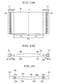
- Fig. 2A is a schematic plan view of a light guide plate and light sources used in the inventive planar lighting device (hereinafter referred to as backlight unit);
- Fig. 2B is a schematic sectional view of the light guide plate.
- a liquid crystal display device 10 comprises a backlight unit 2, a liquid crystal display panel 4 disposed on the side of the backlight unit closer to the light exit plane, and a drive unit 6 for driving the liquid crystal display panel 4.
- liquid crystal display panel 4 electric field is partially applied to liquid crystal molecules previously arranged in a given direction to change the orientation of the molecules.
- the resultant changes in refractive index in the liquid crystal cells are used to display characters, figures, images, etc., on the liquid crystal display panel 4.
- the drive unit 6 applies a voltage to transparent electrodes in the liquid crystal display panel 4 to change the orientation of the liquid crystal molecules, thereby controlling the transmittance of the light transmitted through the liquid crystal display panel 4.
- the backlight unit 2 is a lighting device for illuminating the whole surface of the liquid crystal display panel 4 from behind the liquid crystal display panel 4 and comprises a light exit plane having substantially a same shape as an image display surface of the liquid crystal display panel 4.
- the backlight unit 2 As illustrated in Figs. 2A and 2B , the backlight unit 2 according to the first embodiment of the present invention comprises two light sources 12, a diffusion film 14, a polarization separator film 16, a light guide plate 18 as a light guide member, a light mixer 20, and a reflection sheet 22. Now, components forming the backlight unit 2 will be described below.
- each light source 12 comprises an LED array 24 and coupling lenses 40.
- the LED array 24 is configured by RGB-LEDs 30 arranged in a row, each RGB-LED 30 being formed using three different light emitting diodes, i.e., red, green, and blue light emitting diodes (each referred to as R-LED 32, G-LED 34, and B-LED 36 below).
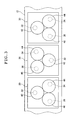
- Fig. 3 schematically illustrates how the RGB-LEDs 30 are arranged.
- the R-LED 32, the G-LED 34, and the B-LED 36 are regularly arranged as illustrated in Fig. 3 .
- each RGB-LED 30 the directions of the optical axes of the three kinds of LEDs (the R-LED 32, the G-LED 34, and the B-LED 36) are adjusted as illustrated in Fig. 4 such that light beams leaving the R-LED 32, the G-LED 34, and the B-LED 36 cross one another at a given position.
- the three kinds of LEDs are thus adjusted such that the light beams from the LEDs are mixed to become white light.
- the RGB-LED 30 configured using LEDs representing three primary colors (the R-LED 32, the G-LED 34, and the B-LED 36) achieves a wide range of color reproduction and a high color purity as compared with cold cathode tubes (CCFL) conventionally used as light source for backlight. Therefore, where the RGB-LED 30 is used as light source for backlight, color reproduction is improved over the prior art and images can be displayed in vivid color representation.
- CCFL cold cathode tubes
- three ball lenses 42, 44, and 46 are disposed as coupling lens on the light emitting side of the respective LEDs of the RGB-LED 30.
- the ball lenses 42, 44, and 46 are disposed for the respective LEDs.
- three ball lenses 42, 44, and 46 are allotted to one RGB-LED 30.
- Light beams leaving the LEDs (the R-LED 32, the G-LED 34, and the B-LED 36) are each collimated by the ball lenses 42, 44, and 46.
- the light beams then cross one another at a given position to become white light and enter a light mixer 20 of the light guide plate 18.
- the coupling lens composed of the three ball lenses 42, 44, and 46 is a lens having three axes, whereby light beams leaving the LEDs of the RGB-LED can be mixed such that said light beams meet at one point.
- ball lenses are used as coupling lens in the example under discussion, no specific limitation is placed thereon, provided that the coupling lens is capable of collimating the light beams emitted by the LEDs.
- One may use, for example, cylindrical lenses, lenticular lenses, half-cylindrical lenses, Fresnel lenses, etc., to form the coupling lens.
- the light guide plate 18 of the backlight unit 2 comprises a flat, substantially rectangular light exit plane 18a, two inclined planes (a first inclined plane 18b and a second inclined plane 18c) located on the opposite side from the light exit plane 18a and inclined a given angle with respect to the light exit plane 18a in such a manner as to be symmetrical to each other with respect to a bisector X parallel to one side of the light exit plane 18a and bisecting the light exit plane 18a, two light entrance planes (a first light entrance plane 18d and a second light entrance plane 18e) located opposite the two LED arrays 24 and admitting light emitted by the LED arrays 24.
- two inclined planes a first inclined plane 18b and a second inclined plane 18c
- the first inclined plane 18b and the second inclined plane 18c are inclined with respect to the light exit plane 18a on both sides of the bisector X.
- the light guide plate 18 grows thicker from the first light entrance plane 18d and the second light entrance plane 18e to the center, and is thickest at the center and thinnest on both ends.
- the light guide plate 18 substantially has a plate-like shape, where the light exit plane 18a is located on the front side (a plane having a large area) of the plate, the first light entrance plane 18d and the second light entrance plane 18e are located on the lateral sides (elongate planes lying in the direction of the thickness) of the plate, and the first inclined plane 18b and the second inclined plane 18c are located on the rear side of the plate.
- first inclined plane 18b and the second inclined plane 18c have prism arrays formed thereon in the direction parallel to the light entrance planes 18d and 18e.
- prism arrays optical elements similar to prisms may be formed regularly.
- elements having lens effects such as lenticular lenses, concave lenses, convex lenses, or pyramid-shaped lenses may be formed on the inclined planes of the light guide plate.
- light entering through the first light entrance plane 18d and the second light entrance plane 18e is scattered by scatterers (described later in detail) contained inside the light guide plate 18 as light travels through the inside of the light guide plate 18 and, directly or after being reflected by the first inclined plane 18b and the second inclined plane 18c, exits through the light exit plane 18a.
- Some light can in the process leak through the first inclined plane 18b and the second inclined plane 18c but is then reflected by the reflection sheet (not shown) covering the first inclined plane 18b and the second inclined plane 18c back into the light guide plate 18.
- the light guide plate 18 is formed of a transparent resin into which scattering particles for scattering light are kneaded and dispersed.
- Transparent resin materials that may be used to form the light guide plate 18 include optically transparent resins such as PET (polyethylene terephthalate), PP (polypropylene), PC (polycarbonate), PMMA (polymethyl methacrylate), benzyl methacrylate, MS resins, and COP (cycloolefin polymer).
- PET polyethylene terephthalate
- PP polypropylene
- PC polycarbonate
- PMMA polymethyl methacrylate
- benzyl methacrylate benzyl methacrylate
- MS resins cycloolefin polymer
- COP cycloolefin polymer
- ⁇ be the scattering cross section of the scattering particles contained in the light guide plate 18
- L G the length of the light guide plate 18 in the direction in which light is admitted from the light entrance plane to a position where the thickness of the light guide plate in the direction perpendicular to the light exit plane is greatest, the length L G being, in the embodiment under discussion, a half of the length of the light guide plate in the direction in which light is admitted (direction perpendicular to the first light entrance plane 18d of the light guide plate 18; also referred to as "direction of the optical axis" below); N p the density of the scattering particles contained in the light guide plate 18 (number of particles in unit volume); and K c a compensation coefficient.
- the light guide plate 18, containing scattering particles satisfying the above relationship, is capable of emitting uniform illumination light through the light exit plane with a reduced level of brightness unevenness.
- ⁇ ⁇ ⁇ N P
- a light extraction efficiency E out is expressed by the following expression (3) where L G is a half of the length of the light guide plate in the direction of the optical axis.
- the length L G a half of the length of the light guide plate in the direction of the optical axis, is the length of the light guide plate 18 in the direction perpendicular to the light entrance planes from one of the light entrance planes of the light guide plate 18 to the center of the light guide plate 18.
- the light extraction efficiency E out is a ratio of light reaching the position distanced from the light entrance plane of the light guide plate by the length L G in the direction of the optical axis to the incoming light.
- the light extraction efficiency E out is a ratio of light reaching the center of the light guide plate (position determined by a half of the length of the light guide plate in the direction of the optical axis) to the light incident on the end faces.
- the expression (3) applies to a space of limited dimensions.
- the compensation coefficient K C is therein introduced.
- the compensation coefficient K C is a dimensionless compensation coefficient empirically obtained where light propagates through an optical medium of limited dimensions.
- the light extraction efficiency E out is then expressed by the following expression (4).
- E out exp - ⁇ ⁇ N p ⁇ L G ⁇ K C
- a light use efficiency as high as 50 % or more is achieved when ⁇ N p ⁇ L G ⁇ K C is 1.1 or greater. While light emitted through the light exit plane 18a of the light guide plate 18 increasingly exhibits illuminance unevenness as ⁇ N p ⁇ L G ⁇ K C increases, the illuminance unevenness can be held to under a given level (within a tolerable range) by holding the value ⁇ N p ⁇ L G ⁇ K C to 8.2 or less. Note that illuminance and brightness can be treated substantially equally. Thus, it is assumed that brightness and illuminance possess similar tendencies in the present invention.
- the value ⁇ N p ⁇ L G ⁇ K C of the inventive light guide plate preferably satisfies a relationship that it is not less than 1.1 and not greater than 8.2, and more preferably not less than 2.0 and not greater than 7.0. Still more preferably, the value ⁇ N p ⁇ L G ⁇ K C is not less than 3.0 and, most preferably, not less than 4.7.
- the compensation coefficient K C is preferably not less than 0.005 and not greater than 0.1.
- the light guide plate will be described in greater detail by referring to specific examples.
- a computer simulation was conducted to obtain light use efficiencies for different light guide plates given different values of ⁇ N p ⁇ L G ⁇ K C by varying the scattering cross section ⁇ , the particle density N p , the length L G , which is a half of the length of the light guide plate in the direction of the optical axis, and the compensation coefficient K c . Further, illuminance unevenness was evaluated.
- the illuminance unevenness [%] was defined as [(I Max - I Min ) /I Ave ] x 100, where I Max was a maximum illuminance of light emitted through the light exit plane of the light guide plate, I Min a minimum illuminance, and I Ave an average illuminance.
- I Max was a maximum illuminance of light emitted through the light exit plane of the light guide plate
- I Min a minimum illuminance
- I Ave an average illuminance.
- Table 1 and Fig. 5 show that given ⁇ N p ⁇ L G ⁇ K c of 1.1 or more, a high light use efficiency, specifically 50 % or more, is achieved whereas given ⁇ N p ⁇ L G ⁇ K c of 8.2 or less, illuminance unevenness can be held to 150 % or less. It is also shown that given K C of 0.005 or more, a high light use efficiency is achieved, and given K C of 0.1 or less, illuminance unevenness observed in light emitted from the light guide plate can be reduced to a low level.
- light guide plates varying in particle density N p of the particles kneaded or dispersed in the light guide plates were constructed to measure brightness distributions of light emitted at different locations in the light exit plane of the individual light guide plates.
- conditions including scattering cross section ⁇ , the length L G , which is a half of the length of the light guide plate in the direction of its optical axis, the compensation coefficient K C , and the shape of the light guide plate, excluding the particle density N p were respectively set to fixed values as the measurements were made.
- ⁇ N p ⁇ L G ⁇ K C changes in proportion as the particle density N p changes.
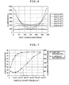
- FIG. 6 shows the measurements of the distribution of illuminance observed in the light emitted through the light exit plane of the individual light guide plates having different particle densities.
- Fig. 6 shows the illuminance [lx] on the vertical axis plotted against the distance [mm] from one of the light entrance planes of the light guide plate (light guiding length) on the horizontal axis.
- illuminance unevenness was calculated from [(I Max - I min )/I Ave ] x 100 [%], where I Max is a maximum illuminance in the measured distribution of light emitted through the side walls of the light guide plate, I Min is a minimum illuminance, and I Ave is an average illuminance.
- Fig. 7 illustrates a relationship between calculated illuminance unevenness and particle density.
- Fig. 7 shows the illuminance unevenness [%] on the vertical axis plotted against the particle density [pieces/m 3 ] on the horizontal axis.
- Also shown in Fig. 7 is a relationship between light use efficiency and particle density, the particle density being likewise indicated on the horizontal axis and the light use efficiency [%] on the vertical axis.
- At least one surface of the first light entrance plane 18d and the second light entrance plane 18e, through which light is admitted, the light exit plane 18a, and the first inclined plane 18b and the second inclined plane 18c, which reflect light preferably has a surface roughness Ra of smaller than 380 nm, thus, Ra ⁇ 380 nm.
- Ra surface roughness
- the light exit plane 18a is given a surface roughness Ra of smaller than 380 nm
- transmission by diffuse reflection through the surfaces of the light guide unit can be ignored or, in other words, transmission by diffuse reflection on the surfaces of the light guide unit can be prevented and, therefore, light is allowed to travel further deep into the light guide unit by total reflection.
- the first inclined plane 18b and the second inclined plane 18c, which reflect light is given a surface roughness Ra of smaller than 380 nm
- diffuse reflection can be ignored or, in other words, diffuse reflection on these reflective surfaces can be prevented and, therefore, all the reflected light components are allowed to travel further deep into the light guide unit.
- D1 be the thickness of the light guide plate at its light entrance plane (thickness at the light entrance) and D2 the thickness of the light guide plate at the plane located on the side opposite from the light entrance plane (thickness at the center), and L the length of the light guide plate in the direction in which light is admitted (light guiding length).
- the light emission efficiency can be increased to 30 % or more.
- the following relationships preferably hold: D ⁇ 1 ⁇ D ⁇ 2 and 66 / 100000 ⁇ D ⁇ 2 - D ⁇ 1 / L / 2 ⁇ 26 / 1000 and the ratio Npa of the weight of the contained scattering particles to the weight of the light guide plate preferably satisfies a range: 0.04 % Wt ⁇ Npa ⁇ 0.25 % Wt .
- the light emission efficiency can be increased to 40 % or more.
- the following relationships preferably hold: D ⁇ 1 ⁇ D ⁇ 2 and 1 / 1000 ⁇ D ⁇ 2 - D ⁇ 1 / L / 2 ⁇ 26 / 1000 and the ratio Npa of the weight of the contained scattering particles to the weight of the light guide plate preferably satisfies a range of: 0.04 % Wt ⁇ Npa ⁇ 0.25 % Wt .
- the shape satisfies the above relationships, the light emission efficiency can be increased to 50 % or more.
- Fig. 8 shows measurements of light use efficiencies of light guide plates having different inclination angles of the inclined planes, i.e., light guide plates having various shapes with different (D2 - D1)/(L/2).
- Fig. 8 indicates (D2 - D1)/(L/2) of the light guide plate on the horizontal axis plotted against light use efficiency [%] on the vertical axis.
- the light use efficiency can be increased to 30 % or more; that when the light guide plate has a shape satisfying 66/100000 ⁇ (D2 - D1)/(L/2) ⁇ 26/1000, the light use efficiency can be increased to 40 % or more; and that when the light guide plate has a shape satisfying 1/1000 ⁇ (D2 - D1)/(L/2) ⁇ 26/1000, the light use efficiency can be increased to 50 % or more.
- the two inclined planes (the first inclined plane 18b and the second inclined plane 18c) of the light guide plate 18, in the embodiment under discussion, have prism arrays formed thereon for efficient reflection of light
- the prism arrays need not necessarily be formed and the inclined planes may be allowed to have a flat surface without an asperity formed thereon.
- the present invention is not limited thereto; the light guide plate may have any shape, provided that the light guide plate is thicker at the plane opposite the light entrance plane than at the light entrance plane.
- the plane of the light guide plate opposite the light exit plane may be a curved surface.
- the inclined plane is formed to be a curved plane, it may be curved outward or inward with respect to the light exit plane.
- Figs. 9A to 9D are schematic sectional views illustrating other examples of the light guide plate.
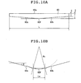
- Fig. 10A is a schematic sectional view illustrating another example of the light guide plate;
- Fig. 10B is a schematic sectional view illustrating a part near the joint of the inclined planes of the light guide plate of Fig. 10A as enlarged.
- a first inclined plane 204 comprises a first inclined portion 206 located closer to the light entrance plane 18d and a second inclined portion 208 located closer to the center of the light guide plate.
- the first inclined portion 206 and the second inclined portion 208 are inclined by different angles from each other with respect to the light exit plane such that the inclination angle of the first inclined portion 208 is smaller than the inclination angle of the second inclined portion 206.
- the first inclined plane is formed with inclined portions of which the inclination angles grow smaller toward the center of the light guide plate.
- a second inclined plane 204' is symmetric to the first inclined plane 204 and comprises a first inclined portion 206' located closer to the light entrance plane 18e and a second inclined portion 208' located closer to the center of the light guide plate and having an inclination angle smaller than that of the first inclined portion 206'.
- each inclined plane consists of two inclined portions in Fig. 9A
- the number of inclined portions forming the inclined plane is not limited specifically; each inclined plane may be composed of any number of inclined portions, provided that the inclination angle grows gradually smaller toward the center of the light guide plate. As illustrated in Fig.
- a first inclined portion 212 (a second inclined portion 212') of a light guide plate 210 may be formed with three inclined portions: a first inclined portion 214 (214'), a second inclined portion 216 (216') having a smaller inclination angle than the first inclined portion 214 (214'), and a third inclined portion 218 (218') having a smaller inclination angle than the second inclined portion 216 (216'), arranged from the first light entrance plane 18d (the second light entrance plane 18e) toward the center of the light guide plate.
- a light guide plate 220 illustrated in Fig. 9C comprises a rounded portion 222a at the end of a first inclined plane 222 closer to the first light entrance plane 18d, i.e., at the joint of the first inclined plane 222 with the first light entrance plane 18d.
- a second inclined plane 222' also has a rounded portion 222a' at its end closer to the second light entrance plane 18e.
- a light guide plate 230 illustrated in Fig. 9D has a first inclined plane 232 and a second inclined plane 232' formed into an aspherical shape that may be expressed by a 10-th order polynomial.
- the increase in brightness of light emitted at the area of the light exit plane near the light entrance planes can be prevented also by forming the inclined planes into an aspherical shape.
- a light guide plate 60 preferably has a curved or rounded joint 60f between a first inclined plane 60b and a second inclined plane 60c (the central portion of the inclined planes of the light guide plate) allowing a smooth connection. This prevents occurrence of bright lines or dark lines at the joint 60f between the first inclined plane 60b and the second inclined plane 60c, and enables emission of light with an increased uniformity.
- the joint 60f between the inclined planes 60b and 60c of the light guide plate 60 i.e., the central part of the light guide plate 60
- the relationship between the radius of curvature R 1 which is a radius of curvature of the rounded shape
- the length L of the light guide plate in the direction in which light is admitted preferably satisfies 3L ⁇ R 1 ⁇ 500L.
- 2R 1 ⁇ sin ( ⁇ ) ⁇ L R preferably holds, where L R denotes the length of the rounded portion of the joint 60f from one end thereof to the other in the direction in which light is admitted, and ⁇ denotes the angle formed by a plane parallel to a light exit plane 60a and the first inclined plane 60b (or the second inclined plane 60c).
- L R is not smaller than 2R 1 ⁇ sin ( ⁇ ) ⁇ L, the decrease in brightness at the central part can be prevented and light with an increased uniformity can be emitted through the light exit plane.
- the light guide plate preferably has a shape satisfying 3L ⁇ R 1 ⁇ 500L and 2R 1 ⁇ sin ( ⁇ ) ⁇ L R ⁇ 0.98L.
- the angle ⁇ can be represented by the following expression (D) using a maximum thickness t max of the light guide plate 60, a minimum thickness t min , and the length L of the light guide plate in the direction in which light is admitted.
- ⁇ tan - 1 ⁇ t max - t min L / 2
- the light guide plate may be made by mixing a plasticizer into the transparent resin described earlier.
- the light guide plate made of materials containing a transparent material mixed with a plasticizer is given a flexibility, or a pliability such that the light guide plate can be formed into various shapes.
- the surface of the light guide plate can be formed into various curved surfaces. Therefore, in cases where, for example, the light guide plate or a planar lighting device using the light guide plate is used as a display board employing ornamental lighting (illuminations), it can also be mounted to a wall having a curvature.
- the light guide plate can be used for a wider variety of applications and in a wider application range including ornamental lighting and POP (point-of-purchase) advertising.
- Said plasticizer is exemplified by phthalic acid esters, or, specifically, dimethyl phthalate, diethyl phthalate(DEP), dibutyl phthalate (DBP), di(2-ethylhexyl) phthalate (DOP (DEHP)), di-n-octyl phthalate (DnOP), diisononyl phthalate (DINP), dinonyl phthalate (DNP), diisodecyl phthalate (DIDP), phthalate mixed-base ester (C 6 to C 11 ) (610P, 711P, etc.) and butyl benzyl phthalate (BBP).
- phthalic acid esters or, specifically, dimethyl phthalate, diethyl phthalate(DEP), dibutyl phthalate (DBP), di(2-ethylhexyl) phthalate (DOP (DEHP)), di-n-octyl phthalate (DnOP), dii
- said plasticizer is also exemplified by dioctyl adipate (DOA), diisononyl adipate (DINA), dinormal alkyl adipate (C 6 , 8 , 10 ) (610A), dialkyl adipate (C7,9) (79A), dioctyl azelate (DOZ), dibutyl sebacate (DBS), dioctyl sebacate (DOS), tricresyl phosphate (TCP), tributyl acetylcitrate (ATBC), epoxidized soybean oil (ESBO), trioctyl trimellitate (TOTM), polyesters , and chlorinated paraffins.
- DOA dioctyl adipate
- DINA diisononyl adipate
- C 6 , 8 , 10 dinormal alkyl adipate
- C7,9 dialkyl adipate
- DOZ dioctyl a
- the backlight unit 2 has light mixers 20A and 20B provided on both sides of the light guide plate 18 in close contact therewith.
- the light mixers 20A and 20B are columnar optical members formed of a transparent resin containing light scattering particles mixed therein and have a function to mix incoming light admitted through the coupling lenses 40.
- the light mixers 20A and 20B may basically be formed of a same material as the light guide plate 18 and may contain scattering particles for scattering light inside. The density, etc., of the scatterers contained in the light mixers 20A and 20B may be identical to or different from those of the scatters contained in the light guide plate 18.
- the light mixers 20A and 20B, located close to the LED array 24s as illustrated in Fig. 2 are preferably formed of a material having a great heat resistance.
- the polarization separator film 16 in a preferred embodiment preferably is integrally formed with the light guide plate 18 on the light exit plane 18a, which is a plane located on the light emitting side of the light guide plate 18.
- the polarization separator film 16 is capable of selectively transmitting a given polarized component, e.g., p-polarized component, of light emitted through the light exit plane of the light guide plate and reflecting almost all of the other polarized components, e.g., s-polarized component.
- the polarization separator film 16 causes reflected light to reenter the light guide plate for reuse, which greatly increases light use efficiency and enhances brightness.
- the polarization separator film 16 may for example be obtained by mixing, kneading, and dispersing acicular particles into a transparent resin and stretching a resultant sheet material to orient the acicular particles in a given direction.
- the polarization separator film 16 preferably is integrated with the light guide plate 18 by compression or fusion at the time of manufacture. Thus, the light exit plane 18a of the light guide plate 18 and the polarization separator film 16 can be brought into close contact without allowing air therebetween.
- the polarization separator film 16 is integrated with the light guide plate 18 in the above example, the present invention is not limited thereto; the polarization separator film 16 and the light guide plate 18 may be manufactured each separately, bonding the polarization separator film 16 to a surface located on the light emitting side of the light guide plate 18. While the polarization separator film 16 is provided immediately on the light exit plane of the light guide plate 18 in the illustrated example, the present invention is not limited thereto; the polarization separator film 16 may be provided on the diffusion film. In this case, the polarization separator film 16 may be integrated with the diffusion film.
- the polarization separator film 16 may be a known polarization separator film.
- a birefringent material having a refractive index greater than that of the light guide plate at the light exit plane thereof with respect to at least one plane of polarization and having a refractive index lower than an average refractive index of the light guide plate with respect to a plane of polarization perpendicular to said plane of polarization, as described in JP 06-331824 A .
- the film is preferably bonded to one of both surfaces of the light guide plate by means of an adhesive layer or a bond layer as described in JP 11-281975 A .
- a multilayered structure composed of transparent media having a relatively high refractive index and transparent media having a relatively low refractive index laminated alternately on one another, a planar transparent base material having formed on at least one of both surfaces thereof at least one layer of dielectric film having a thickness of preferably not greater than 1000 nm, or a multilayered transparent polymers having different refractive indices, as described in JP 07-49496 A .
- a polarization separator comprising a transparent base material having a substantially W-shaped cross section provided with at least one layer of dielectric thin film having a thickness not greater than a wavelength of visible light, said polarization separator transmitting the p-polarized component of light adjacent a given incident direction, while reflecting at least part of the s-polarized component of light, as described in JP 07-72475 A .
- a retroreflective polarizer as described in JP 2004-78234 A comprising a first material, a second material, and at least one optical deposit.
- the first material has a structured surface consisting of linear arrays of juxtaposed prisms each having an essentially isosceles coefficient with a substantially right angle and each having a plane of vertical coefficient forming an angle of about 45° with respect to a tangential plane to the smooth surface on the side opposite from said structured surface; the second material is essentially the same as the first material.
- Said at least one optical deposit lies on the structured surface of at least one of said materials and is composed of alternately accumulated layers of high refractive index materials and low refractive index materials having selected optical thicknesses.
- the first and the second materials are all optically joined to form a single unit where the refractive indices of the first and the second materials and said refractive indices and optical thicknesses of the layers forming said optical deposit are all so selected as to cause selective reflection of polarized light such that incoming mixed beams of polarized light are separated into an s-polarized component and a p-polarized component inside a part of said optical deposit.
- Said s-polarized component is reflected by the other part of said optical deposit in a direction parallel to the incident light in said other part, then traveling in the opposite direction to the incident light.
- Said p-polarized component is transmitted parallel to the incident light.
- a polarizing element comprising a transparent material having a triangular wave shape formed thereon with alternately provided A-shaped ridges and V-shaped grooves and a multilayered dielectric films having a polarizing filter function and a retardation function provided on said transparent material.
- a multilayered polarizing film as described in US 3610729 B comprising successively laminated, alternating layers of birefringent materials each having a thickness of one quarter of various wavelengths.
- a polymeric optical film as described in US 5867316 B comprising a continuous phase and a small amount of dispersed phase inside the continuous phase.
- a polarization separator film as described in JP 2003-295183 A comprising a metal thin film using surface plasmon sandwiched by transparent media having a low refractive index.
- brightness can be further improved by a configuration of the light guide plate integrated with a polarization direction changing film for changing the polarization direction of light, such as a ⁇ /4 phase-film having a slightly birefringent property causing a difference of ⁇ /4 in optical thickness between mutually perpendicular polarized light components or a diffusing film, in addition to providing a polarization separator film using surface plasmon that transmits only the p-polarized component parallel to the incident plane and reflects the s-polarized component perpendicular to the incident plane.
- polarization separator film 16 In place of the polarization separator film 16, one may use a scattering type polarizing film using anisotropic scatterers formed by stretching a compound material of liquid crystal and a polymer as described in JP 08-76114 A or one may use as the polarization separator film 16 a cholesteric polarizing film where the axis of the molecular helix is so oriented as to extend across the film and the pitch of the molecular helix in the film varies by a difference of at least 100 nm between a maximum pitch and a minimum pitch, as described in JP 06-281814 A .
- a haze anisotropic layer where the value of the haze varies with the vibration direction of the linear polarized light as described in JP 2001-343612 A .
- a polarizing element as described in JP 09-274108 A comprising minute regions formed of a material different from that of a transparent polymer film in which said minute regions are evenly dispersed, the polymer film and the minute regions having approximately a same refractive index with respect to one of the mutually perpendicular linear polarized light beams and different refractive indices with respect to the other.
- brightness of light emitted through the light exit plane can also be improved by forming a micro-asperity having a polarization separator function on the light exit plane of the light guide plate, as described in JP 2001-201746 A and JP 2001-228474 , instead of providing the polarization separator film.
- Brightness may also be improved by forming a roughened surface pattern on the inclined rear surfaces of the light guide plate consisting of fine projections and having a polarization separator function, as described in JP 2004-363062 A .
- the refractive indices of these materials are determined such that either no or ne is equal or virtually equal to np.
- the polarized beams of light can be separated at a boundary surface between the isotropic material and the anisotropic material such that a majority of the light radiated from the light source can be converted into light having a same polarization direction before leaving the light waveguide path.
- brightness can also be improved by applying the configuration described in JP 10-508151 A to the present invention. Further, brightness can also be improved by forming the light guide plate with two or more layers having a light guiding function such that at least one of a first layer and a second layer has a birefringent property and that an interface is provided between the first and the second layers, thereby emitting light that is scattered, refracted or diffracted at the interface through a surface of the light guide plate, as described in JP 09-292530 A .
- the reflection sheet 22 of the backlight unit is provided to reflect light leaking through the inclined planes 18c and 18d of the light guide plate 18 back into the light guide plate 18, thereby enhancing the light use efficiency.
- the reflection sheet 22 is bent at the middle thereof to cover the inclined planes 18c and 18d of the light guide plate 18.
- the reflection sheet 22 may be formed of any material that is capable of reflecting light leaking through the inclined planes 18c and 18d of the light guide plate 18. It may be formed, for example, of a resin sheet formed by kneading PET, PP (polypropylene), etc.
- the diffusion film 14 is disposed between the polarization separator film 16 and the liquid crystal display panel 4.
- the diffusion film 14 is formed by imparting a light diffusing property to a material in the form of film.
- the material in the form of film may be formed of an optically transparent resin such as PET (polyethylene terephthalate), PP (polypropylene), PC (polycarbonate), PMMA (polymethyl methacrylate), benzyl methacrylate, an MS resin, or COP (cycloolefin polymer).
- the method of manufacturing the diffusion film 14 is not limited specifically.
- a surface of the material in the form of film may be machined to form an asperity thereon or roughened by grinding thereby to provide a light diffusing property, or by coating the surface with a material that diffuses light as exemplified by silica; pigments such as titanium oxide and zinc oxide; a resin; and beads of glass, zirconia, etc., together with a binder, or by kneading the above pigments or beads having a light diffusing property into said transparent resin.
- a material having a high reflectance and a low light-absorbing property such as metals as exemplified by Ag and Al.
- a diffusion film of a matte type or a coating type may be used as the diffusion film 14.
- the diffusion film 14 may be disposed a given distance apart from the light exit plane of the light guide plate 18. The distance may be altered as appropriate according to the light amount distribution of light emitted through the light exit plane of the light guide plate 18. With the diffusion film 14 spaced a given distance apart from the light exit plane of the light guide plate 18, the light emitted from the light exit plane of the light guide plate 18 is further mixed (blended) between the light exit plane and the diffusion film 14. This further enhances the uniformity of brightness of light transmitted through the diffusion film 14 to illuminate the liquid crystal display panel 4.
- the diffusion film 14 may be spaced a given distance apart from the light exit plane of the light guide plate 18 using a method, for example, whereby spacers are provided between the diffusion film 14 and the light guide plate 18.
- the present invention is by no means limited thereto. While the above embodiment uses the red, green, and blue LEDs 32, 34, and 36, and light beams emitted by the individual LEDs are mixed by the coupling lens 40 to obtain white light, the present invention is not limited thereto.
- the light source may use a monochromatic LED whose emitted light is converted into white light through a fluorescent substance. Where a GaN base blue LED is used as a monochromatic LED, for example, white light can be obtained using a YAG (yttrium aluminum garnet) base fluorescent substance. Such light source whereby white light can be obtained eliminates the need to use lenses and, hence, reduces the number of components required.
- Fig. 11A is a schematic plan view illustrating an embodiment of the planar lighting device (backlight) using monochromatic LEDs as light source;
- Fig. 11B is a schematic sectional view of the planar lighting device. Except for light sources 122, the components of a backlight unit 120 illustrated in Figs. 11A and 11B have similar configurations to those of the backlight unit 2 of Fig. 1 . Accordingly, like components share like reference characters between the two, and detailed descriptions thereof will not be given here, focusing instead on features unique to the backlight unit 120 below.
- the light sources 122 comprise LED arrays 124 and coupling lenses 126 and are disposed opposite the first light entrance plane 18d and the second light entrance plane 18e as illustrated in Fig. 11A .
- LED chips 128 are disposed in a row at given intervals on a heat sink 130.
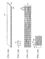
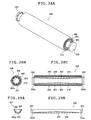
- Fig. 12A is a schematic perspective view illustrating a configuration of the LED array 124;
- Fig. 12B is a schematic top view of a configuration of an LED chip 128;
- Fig. 12C is a schematic plan view of a configuration of multilayered LED array 132; and
- Fig. 3D is a schematic side view of an embodiment of a heat sink 25.
- the LED chip 128 is a monochromatic LED configured such that light emitted by an LED thereof is converted into white light using the fluorescent substance mentioned earlier.
- the heat sink 130 is a sheet member parallel to one side of the light guide plate 18 and disposed opposite the light guide plate 18.
- the heat sink 130 carries LED chips 128 on a surface thereof facing the light guide plate 18.
- the heat sink 130 is formed of a metal having a good thermal conductivity such as copper or aluminum to absorb and release heat generated by the LED chips 128 to the outside.
- the heat sink 130 preferably has a shape such that, as in the embodiment under discussion, the length thereof in the direction perpendicular to the plane thereof facing the first light entrance plane and the second light entrance plane of the light guide plate 18 is longer than the length of the plane thereof facing the first light entrance plane and the second light entrance plane of the light guide plate 18 in the direction of the shorter sides. This increases the efficiency with which the LED chips 128 are cooled.
- the heat sink preferably has a large surface area.
- the heat sink 130 may be configured for example by a base 130a carrying the LED chips 128 and a plurality of fins 130b joined to the base 130a as illustrated in Fig. 12D .
- a plurality of fins 130b provided secure a large surface area and a high heat dissipation efficiency, increasing the efficiency with which the LED chips 128 are cooled.
- the heat sink may be not only of air-cooled type but also of water-cooled type. While the embodiment under discussion uses a heat sink as a support member for the LED chips, the present invention is not limited thereto: where the LED chips need not be cooled, a sheet member without a heat-releasing function may be used as the support member.
- the LED chip 128 has a rectangular shape such that the sides perpendicular to the direction in which the LED chips 128 are arrayed are shorter than the sides lying in the direction in which the LED chips 128 are arrayed or, in other words, the sides lying in the direction of thickness of the light guide plate 18 (the direction perpendicular to the light exit plane 18a) are the shorter sides.
- the LED chip 128 has a shape satisfying b > a where "a" denotes the length of the sides perpendicular to the light exit plane 18a of the light guide plate 18 and "b" denotes the length of the sides in the direction of the array.
- the LED chips each preferably have a rectangular shape with the shorter sides lying in the direction of thickness of the light guide plate to achieve a thinner design of the LED array
- the present invention is not limited thereto, allowing use of LED chips having any shape as appropriate such as a square, a circle, a polygon, and an ellipse.
- the LED array is monolayered in the embodiment under discussion, the present invention is not limited thereto; one may use a multilayered LED array 132 comprising a plurality of LED arrays 124 for the light source as illustrated in Fig. 12C .
- the LEDs are thus stacked, more LED arrays can be stacked when the LED chips are each given a rectangular shape and the LED arrays each have a reduced thickness.
- the LED arrays are stacked into a multilayer, that is to say, where more LED arrays (LED chips) are packed into a given space, an increased amount of light can be generated.
- the above expression also applies to the distance separating the LED chips of an LED array from the LED chips of the LED arrays in adjacent layers.
- the LED arrays preferably are stacked such that the LED chips are spaced a given distance apart from the LED chips of the LED arrays in adjacent layers.
- ball lenses are provided as coupling lenses 126 on the light emitting side of the respective LED chips 128 of the LED array 124.
- the coupling lenses 126 are provided for the respective LED chips 128.
- Light emitted by the individual LED chips 128 is collimated by the coupling lenses 126 before entering the light mixer 20 of the light guide plate 18.
- ball lenses are used as coupling lenses here, one may use various types of members capable of collimating light emitted by the LEDs other than ball lenses.
- One may use, for example, a cylindrical lens, a lenticular lens, a half-cylindrical lens, a Fresnel lens, etc.
- light guides may be used to lead light emitted by the LEDs of the LED arrays 24 to the light guide plate.
- the light guides may be formed, for example, of optical fibers and light guide paths made of a transparent resin. Where the LED arrays 24 are used as light source and located close to the lateral planes of the light guide plate 18, heat generated by the LEDs forming the LED array 24 may possibly deform or melt the light guide unit 18.
- Deformation and melting of the light guide 18 due to the heat generated by the LEDs can be prevented by locating the LED arrays 24 away from the lateral planes of the light guide plate 18 and leading light emitted by the LEDs as far as the light guide plate 18 through the light guides.
- the light source using LEDs include one where blue LEDs are used with a red-green fluorescent substance. Specifically, one may use a fluorescent element where the LEDs are used with a fluorescent substance as described in JP 2005-228996 A . Alternatively, one may use a light source where red LEDs are used with red, green, and blue fluorescent substances. Examples of such light source include a light emitting device where an LED is used with a fluorescent substance as described in JP 2000-347691 A , a white light emitting diode where an LED is used with fluorescent substances as described in JP 2002-43633 A , and a light emitting device where an LED is used with fluorescent substances as described in JP 2005-126577 A .
- the present invention is not limited to providing a fluorescent substance opposite the light emission face of the LED to radiate white light; emission of white light through the light exit plane is also achieved by mixing a fluorescent substance into the light guide plate instead of providing a fluorescent substance opposite the light emission face of the LED.
- the heat sink of the LED array is shaped like a flat plate and disposed on the rear side of the LED chip to extend parallel to the light exit plane in the above embodiment, it may alternatively be formed into a bent shape like a letter L, for example, in such a manner as to extend from behind the LED chip toward the inclined plane of the light guide plate, i.e., over the rear side of the reflection member. This serves to reduce the area of the planar lighting device lying in the direction parallel to the light exit plane.
- the heat sink is formed into a bent shape and disposed on the side of the light guide plate closer to the inclined plane, the heat sink preferably has a thickness and/or a length that does not affect the thickness of the backlight unit.
- the heat sink may be formed of a material having a high thermal conductivity such as, for example, aluminum or copper, as described earlier as well as various other materials.
- the heat sink thermally communicates with the housing, which supports the light guide plate, the reflection members, the LED arrays, and the like from the outside.
- the heat sink preferably communicates thermally with the housing.
- the heat sink thermally communicates with the housing, heat generated by the LED chips can be released from the whole backlight unit (planar lighting device).
- the heat sink and the housing need not necessarily be in immediate contact with each other; they may be in contact with each other via a thermal connector.
- Fig. 13 schematically illustrates a configuration of the backlight unit where a prism sheet 26 is disposed on the light exit plane 18a of the light guide plate 18.
- the light guide plate 18, the polarization separator film 16, and the prism sheet 26 are formed integrally.
- the prism sheet 26 is a transparent sheet formed by prisms arranged parallel to one another and helps condense light emitted through the light exit plane of the light guide plate 18 to improve brightness.
- the light guide plate 18, the polarization separator film 16, and the prism sheet 26 may be integrated by a method whereby, for example, the polarization separator film 16 and the prism sheet 26 are integrated into a sheet first, whereon the sheet is united with the light guide plate 18 by fusion or compression at the time of manufacture of the light guide plate 18.
- the polarization separator film 16 may be integrated with the prism sheet 26 by a method whereby, for example, the polarization separator film 16 and the prism sheet 26 are manufactured separately and simply bonded to each other, or by a method whereby a polarization separator sheet material is fed to the molding rolls of a continuous extruder, whereon the polarization separator film is fused to the extruded prism sheet.
- the prism sheet may be provided between the polarization separator film 16 and the diffusion sheet 14 of the backlight unit illustrated in Fig. 1 comprising the light guide plate 18 having prism arrays formed on the first inclined plane 18b and the second inclined plane 18c.
- the prism sheet is composed of a single sheet in the example illustrated in Fig. 13 , it may be composed of two sheets.
- one of the two prism sheets is disposed such that the prism arrays thereof extend parallel to the light entrance planes (the first light entrance plane and the second light entrance plane) of the light guide plate 18; the other is disposed with the prism arrays extending perpendicular thereto.
- the two prism sheets are disposed such that their respective prism arrays extend perpendicular to each other.
- the prism sheets are preferably disposed such that the vertexes of the prisms face the polarization separator film 16.
- the order in which the prism sheets are disposed is not specifically limited. To be more specific, one may dispose the prism sheet having prisms extending parallel to the light entrance plane of the light guide plate 18 immediately on the polarization separator film 16 while overlaying on that prism sheet the other prism sheet having prisms extending perpendicular to the light entrance plane of the light guide plate 18, or the prism sheets may be disposed in the reversed order. While the illustrated example uses the prism sheet 26, a sheet on which optical elements similar to prisms are arranged regularly may be used instead of the prism sheet 26.
- a plurality of diffusion films may be used without using the prism sheet. Then, two or more, preferably three diffusion films are used.
- a plurality of diffusion reflectors 140 may be formed, by printing for example, on the first inclined plane 18b and the second inclined plane 18c of the light guide plate 18 in a given pattern, specifically in such a pattern that the density is low on the end portions of the light guide plate 18, i.e., close to the first light entrance plane 18d and the second light entrance plane 18e, growing gradually higher toward the center of the light guide plate 18.
- Such diffusion reflectors 120 formed on the inclined plane 18b of the light guide plate 18 in a given pattern limit generation of bright lines or unevenness on the light exit plane 18a of the light guide plate 18.
- a thin sheet having the diffusion reflectors 140 formed thereon in a given pattern may be disposed between the first inclined plane 18b and the second inclined plane 18c of the light guide plate 18 and the reflection sheet 22.
- the diffusion reflectors 140 may each have any shape such as a rectangle, a polygon, a circle, and an ellipse.
- the diffusion reflectors 140 may be formed, for example, by applying a material for diffusing light as exemplified by silica; pigments such as titanium oxide and zinc oxide; a resin; and beads of glass, zirconia, etc., together with a binder, or may be a pattern created by machining the surface to form an asperity thereon or by grinding to roughen the surface. Otherwise, one may use a material having a high reflectance and a low light-absorbing property such as metals as exemplified by Ag and Al. One may also use ordinary white ink as used in screen printing, offset printing, etc., to form diffusion reflectors.
- the diffusion reflectors are distributed in a density that increases with the increasing distance from the light entrance plane in the embodiment under discussion, the present invention is not limited thereto and may be determined as appropriate according to the intensity or distribution of bright lines, brightness distribution required of emitted light, etc.
- the diffusion reflectors may be distributed evenly on the whole surface of the inclined planes or in a density that increases with the increasing distance from the light entrance planes. Further, instead of providing the diffusion reflectors by printing, the positions corresponding to the locations of the diffusion reflectors may be roughened to provide sand-rubbed surfaces.
- the diffusion reflectors are provided on the inclined planes in the light guide plate of Fig. 14 , the present invention is not limited thereto; the diffusion reflectors may be provided on any plane as desired except the light entrance planes.
- planar lighting device may be provided on the light emitting side thereof with a transmittance adjusting member having a function to reduce brightness unevenness of light emitted through the light exit plane.
- Fig. 15 is a schematic sectional view of a planar lighting device 180 provided with a transmittance adjusting member 182.
- the planar lighting device 180 comprises light sources 190, the diffusion film 14, the light guide plate 18, the reflection sheet 22, the transmittance adjusting member 182, and a prism sheet 188.
- the diffusion film 14, the light guide plate 18, and the reflection sheet 22 have the same functions as the diffusion film, the light guide plate, the reflection sheet of Fig. 13 and, therefore, detailed description thereof will not be given here.
- the light sources 190 have substantially the same configuration as the LED arrays 124 each comprising the LED chips 128 and the heat sink 130 described earlier; in the embodiment under discussion, the LED arrays 124 are disposed opposite the first light entrance plane 18d and the second light entrance plane 18e of the light guide plate 18.
- the coupling lenses and the light mixers are not provided between the LED arrays 124 and the first light entrance plane 18d and the second light entrance plane 18e.
- light emitted from the LED arrays 124 enters the light guide plate 18 directly.
- the transmittance adjusting member 182 On the light exit plane 18a of the light guide plate 18 are laid the transmittance adjusting member 182, the diffusion film 14, and the prism sheet 188 in this order on one another.
- the prism sheet 188 has substantially the same function and shape as the prism sheet 26 described above and is disposed such that the vertexes of the prisms face the diffusion sheet 14 or, expressed otherwise, the base of the prisms are parallel to the light entrance plane 18a of the light guide plate 18.
- the transmittance adjusting member 182 is used to reduce brightness unevenness of light emitted from the light guide plate and comprises a transparent film 184 and numerous transmittance adjusters 186 arranged on the surface of the transparent film 184.
- the transparent film 184 is in the form of a film and formed of optically transparent resins such as PET (polyethylene terephthalate), PP (polypropylene), PC (polycarbonate), PMMA (polymethyl methacrylate), benzyl methacrylate, MS resins, other acrylic resins or COP (cycloolefin polymer).
- optically transparent resins such as PET (polyethylene terephthalate), PP (polypropylene), PC (polycarbonate), PMMA (polymethyl methacrylate), benzyl methacrylate, MS resins, other acrylic resins or COP (cycloolefin polymer).
- the transmittance adjusters 186 are dots of various sizes each having a given transmittance and have various shapes such as a rectangle, a circle, and a hexagon; the transmittance adjusters 186 are formed, by printing for example, on the whole surface of the transparent film 184 facing the light guide plate 18 in a given pattern, or in such a pattern, for example, that the sizes of dots or the number of dots vary according to the location (halftone dot pattern).
- the transmittance adjusters 186 need only be diffusion reflectors and may, for example, be formed by applying a material that diffuses light as exemplified by silica; pigments such as titanium oxide and zinc oxide; a resin; and beads of glass, zirconia, etc., together with a binder, or may be a pattern created by machining a surface to form an asperity thereon or by grinding a surface to roughen the surface. Otherwise, one may use a material having a high reflectance and a low light-absorbing property such as metals as exemplified by Ag and Al. One may also use ordinary white ink as used in screen printing, offset printing, etc.
- Numerous transmittance adjusters 186 are distributed on the surface of the transparent film 184 facing the light guide plate unit 18 in a given pattern such that the pattern density of the transmittance adjusters 186 varies according to the location on the surface.
- ⁇ (x, y) be the pattern density of the transmittance adjusting member 182 at a given position (x, y) and F (x, y) be the relative brightness of light emitted at a given position (x, y) on the light exit plane of the backlight unit 180 (plane facing the liquid crystal display panel 4) having no transmittance adjusting member 182.
- the relationship between the pattern density ⁇ (x, y) of the transmittance adjusting member 182 and the relative brightness F(x, y) preferably satisfies the following expression (5).
- F max denotes a maximum brightness
- F min denotes a minimum brightness, of light emitted through the light exit plane of the diffusion film 14 of the backlight unit 180 without the transmittance adjusting member 182.
- the density of the distribution of the transmittance adjusters is designed according to the above expression, there may be cases where brightness unevenness is observed depending on the angle of observation when the observation is made at an angle other than from the front.
- the calculated density distribution is complemented by a "uniform pattern distribution (bias density pb)." This reduces brightness unevenness and eliminates or reduces angular dependence of brightness unevenness.
- the bias density pb is preferably 0.01 to 1.50 (1 to 150 %).
- the transmittance adjusters are provided in two layers. Specifically, transmittance adjusters having a distribution density of (pb - 1) are further disposed on the transmittance adjusters laid on the entire surface.
- the pattern density ⁇ (x, y) denotes occupancy per unit area (1 mm 2 ) of the transmittance adjusters 186 at a given position (x, y).
- ⁇ (x, y) 1
- the transmittance adjusters 186 are provided on the whole surface within the unit area;
- ⁇ (x, y) 0, no transmittance adjuster 186 is provided within the unit area.
- the transmittance adjusters 186 of the transmittance adjusting member 182 so arranged as to satisfy the pattern density ⁇ (x, y) defined by the above expression (5) limit the lowering of the average brightness of light emitted through the light exit plane of the backlight unit 180 and reduces the brightness unevenness.
- the diffusion sheet 14 need not achieve thorough diffusion of light.
- the diffusion sheet 14 may be made thinner, and the prism sheet need no longer be used, or the number of prism sheets used may be reduced, thus providing a lightweight, low-cost backlight unit.
- the planar lighting device having the transmittance adjusting member will be described in greater detail referring to specific examples.
- the backlight unit 180 according to the example under discussion comprises light sources 190, the diffusion film 14, the light guide plate 18, the reflection film 22, the transmittance adjusting member 182, and the prism sheet 188.
- the light guide plate 18 was configured such that the first light entrance plane 18d and the second light entrance plane 18e had a thickness of 2 mm; the light guide plate 18 had a thickness at the center thereof, i.e., a maximum thickness, of 4 mm; the distance from the first light entrance plane 18d to the second light entrance plane 18e was 300 mm; the distance of the light guide plate 18 in the direction of depth, i.e., the distance of the light guide plate 18 in the direction parallel to the first light entrance plane 18d and parallel to the light exit plane 18a was 500 mm.
- the light guide plate 18 was formed using an acrylic resin having a refractive index of 1.495 as the transparent resin and silicone particles having a refractive index of 1.44 as the scattering particles.
- the scattering particles have a particle diameter of 2000 nm.
- the scattering particles were kneaded and dispersed into the transparent resin in such a manner as to provide a scattering cross section ⁇ of 2.06 x 10 -12 m 2 and a particle density of 220000 pieces/mm 3
- the space between the light sources 190 (LED arrays 124) and the light guide plate 18 measured 0.1 mm.
- the relative brightness F(x, y) of light emitted through the light exit plane of a backlight unit having no transmittance adjusting member was measured using a backlight unit having the same configuration and shape except that no transmittance adjusting member 182 was provided.
- the relative brightness F(x, y) was measured as follows. First, the above backlight unit 180 was secured to an XY stage and a brightness meter was secured vertically to the light exit plane of the backlight unit 180. Brightness at locations on the light exit plane of the backlight unit 180 was measured with the brightness meter to obtain information on brightness at particular locations on the light exit plane of the light guide plate 18. Then, the XY stage is moved to obtain the relationship between location on the light exit plane of the backlight unit 180 and brightness. The maximum brightness of the calculated brightness is denoted by F max and the minimum brightness by F min . With reference to a maximum brightness of 1, the ratios of brightness at individual locations to the maximum brightness F max were expressed by relative brightness F(x, y) for the respective locations.
- Fig. 16 illustrates measurements obtained. Fig. 16 indicates relative brightness on the vertical axis plotted against the distance from the central part of the light guide plate on the horizontal axis.
- the pattern density ⁇ (x, y) for the relative brightness F(x, y) is calculated from the measured maximum brightness F max and minimum brightness F min using the above expression 1.
- Fig. 17 indicates the pattern density ⁇ (x, y) on the vertical axis plotted against the distance from the center (central part) of the light guide plate on the horizontal axis.
- the distribution of the pattern density ⁇ (x, y) was calculated for locations at 5 mm intervals in the widthwise direction; according to the calculated pattern density ⁇ (x, y), transmittance adjusters 186 each measuring 0 to 1 mm in the widthwise direction were arranged as appropriate to construct the transmittance adjusting member 182.
- the transmittance adjusters 182 arranged were formed of white ink having a transmittance of 33 % for a wavelength of 550 nm when the transmittance adjusters are provided on the whole surface or, expressed otherwise, when the pattern density ⁇ (x, y) is 1.
- the relative brightness of light emitted through the light exit plane of the backlight unit 180 was measured with the thus formed transmittance adjusting member 182 provided in the backlight unit 180.
- the relative brightness was measured by the same method whereby said relative brightness F(x, y) was measured.
- Fig. 18 illustrates the measurements obtained.
- Fig. 18 indicates the relative brightness on the vertical axis plotted against the distance from the center (central part) of the light guide unit on the horizontal axis. Also shown for comparison is vertical brightness of light emitted through the light exit plane of a backlight unit having the same configuration except that it is not provided with the transmittance adjusting member 182.
- Fig. 18 shows that the transmittance adjusting member 182 provided reduces brightness unevenness when compared with a case where the transmittance adjusting member 182 is not provided.
- the maximum density c is preferably in the range of 0.5 ⁇ c ⁇ 1.
- the maximum density c not smaller than 0.5 curbs the decrease of the average brightness and enables emission of light with enhanced brightness and uniformity.
- the transmittance adjusters may each have any shape including a rectangle, a triangle, a hexagon, a circle, and an ellipse. Where the backlight unit uses linear light sources and a light guide plate shaped by uniaxial drawing as in the example under discussion, the transmittance adjusters may each be shaped into an elongate strip parallel to the axes of the linear light sources.
- the present invention is not limited thereto; the transmittance adjusters may be provided on a diffusion film or a prism sheet.
- the transmittance adjusters may be formed on the diffusion film 14 or the prism sheet 188 illustrated in Fig. 15 instead of the transparent film. This enables reduction of the number of components required and, hence, reduction of manufacturing costs.
- the pattern density distribution of the transmittance adjusters 186 of the transmittance adjusting member 182 are adjusted according to the incident light on the transmittance adjusting member 182.
- the pattern density distribution of the transmittance adjusters 186 may be adjusted by varying the size of the transmittance adjusters 186 or by varying the intervals at which the transmittance adjusters 186, each having a given shape, are arranged.
- the transmittance adjusters 186 may be arranged according to the pattern density by any of various methods including the FM screening method and the AM core method; among these methods, the FM screening method is preferably used.
- the transmittance adjusters 186 can be arranged dispersedly and densely as fine, even-sized dots, making it difficult to visually recognize the arrangement pattern of the transmittance adjusters 186 through the light exit plane of the backlight unit.
- the FM screening method prevents projection of the arrangement pattern of the transmittance adjusters 186 through the light exit plane of the backlight unit and emission of uneven light, thus enabling emission of light with increased uniformity. That method also prevents the dot size from being reduced to such a degree that formation of the transmittance adjusters 186 becomes difficult.
- the transmittance adjusters 186 each have a maximum size of 500 ⁇ m or less, for example, a side of 500 ⁇ m or less when they are rectangular; a major axis of 500 ⁇ m or less when they are elliptical, and more preferably, 200 ⁇ m or less.
- the transmittance adjusters 186 each measuring 500 ⁇ m or less make visual recognition of the shapes of the transmittance adjusters 186 difficult; the transmittance adjusters 186 each measuring 200 ⁇ m or less make visual recognition of the shapes of the transmittance adjusters 186 no longer possible with the result that the shapes of the transmittance adjusters 186, when actually used for a liquid crystal display device, are not projected through the light exit plane of the backlight unit to exhibit brightness unevenness.
- the transmittance adjusters 186 each measure 100 ⁇ m at maximum. A maximum size of 100 ⁇ m reduces the visibility of the size to under a level recognizable by the naked eye with an increased certainty with the result that the shapes of the transmittance adjusters 186, when actually used for a liquid crystal display device, are not projected through the light exit plane of the backlight unit to exhibit brightness unevenness, thus reducing brightness unevenness with an increased certainty and efficiently.
- the transmittance adjusters may be printed on the transparent film by any of various methods including screen printing, offset printing, gravure printing, and ink jet printing.
- Offset printing has an advantage of excellent productivity; screen printing has an advantage that ink thickness can be increased and, hence, a transmittance of the patterned area can be reduced without having to increase the ink concentration.
- Ink jet printing permits printing on a three-dimensional object and, hence, is best suited to form the transmittance adjusters on the surface of the light guide plate.
- alignment marks may be printed on the transparent film outside the area in which the half dot pattern is arranged. The alignment marks formed on the transparent film facilitates alignment of the light guide plate with the transmittance adjusting member at the time of manufacture.
- the transmittance adjusting member is provided between the light guide plate and the diffusion film in the embodiment under discussion, the location is not limited thereto; they may be provided between the diffusion film and the prism sheet. Further, the transmittance adjusting member is provided such that the transmittance adjusters are arranged on the transparent film, the present invention is not limited thereto; the transmittance adjusters may be arranged on the surface of the diffusion film, the prism sheet, or the light guide plate to provide the transmittance adjusting member. Specifically, the transmittance adjusters may be provided on at least one of the surface of the diffusion film closer to the light guide plate (plane through which light is admitted) and the surface of the diffusion film opposite from the light guide plate (plane through which light is emitted).
- the transmittance adjusters may alternatively be provided on at least one of the surface of the prism sheet closer to the light guide plate (plane through which light is admitted) and the surface of the prism sheet opposite from the light guide plate (plane through which light is emitted).
- the transmittance adjusters may be provided immediately on the light exit plane of the light guide plate.
- the transmittance adjusting member can be formed by providing the transmittance adjusters on the surface of the diffusion film, the prism sheet, or the light guide plate without using the transparent film such that the layer configuration can be further simplified.
- the transmittance adjusters can be placed in an accurate position with respect to the brightness unevenness of light emitted from the light guide plate without having to establish an alignment when assembling the planar lighting device.
- the transmittance adjusters are preferably provided in a plurality of locations, i.e., on a plurality of optical members such as, for example, on the surface of the light guide plate and the rear side of the diffusion film, thereby to form a plurality of transmittance adjusting members.
- a plurality of optical members such as, for example, on the surface of the light guide plate and the rear side of the diffusion film.
- the transmittance adjusters are thus provided on a plurality of optical members, the tolerance to misalignment between the arrangement pattern of the transmittance adjusters and the incident light at the individual locations where the transmittance adjusters are provided can be increased, thereby enabling emission of uniform light free from brightness unevenness and uneven coloration.
- the transmittance adjusters may be arranged in the same arrangement pattern or in different arrangement patterns between the locations where they are provided.
- the transmittance adjusters of the transmittance adjusting member are arranged with a pattern density ⁇ (x, y) satisfying the above expression (5) as a preferred embodiment, the present invention is not limited thereto; the transmittance adjusters may be arranged with various pattern densities for curbing the generation of brightness unevenness.
- the transmittance adjusting member may be a known transmittance adjusting member, wherein the transmittance adjusters are arranged in such a manner as to have a density distribution in a direction perpendicular to the axis of the linear light sources.
- a chromaticity adjusting film formed of a transparent film having on its surface white ink mixed with and dispersed into ink of any color (other than white ink) is provided on the light exit plane of the light guide plate.
- the mixing ratio of ink of any color to white ink is less than 1 of ink of any color to 100 of white ink.
- the chromaticity adjusting film provided enables the color of emitted light to be adjusted and color rendition and color reproduction to be improved. Thus, color rendition can also be improved where the light source used can only offer poor color rendition. Further, the color of emitted light can be fine-tuned.
- CCFL cold cathode tubes
- LED elements having a color temperature of 9150 K
- LED elements having a color temperature of 8500 K.
- Measured was the chromaticity of light emitted without using the chromaticity adjusting film and the chromaticity of light emitted using chromaticity adjusting films with different ink mixing ratios given in Tables 2 and 3 below.
- Figs. 19 to 21 illustrate the measurements obtained.
- Fig. 19 is a graph illustrating the measurements of light emitted by cold cathode tubes (CCFL) having a color temperature of 3500 K and transmitted through the chromaticity adjusting films given in Tables 2 and 3;
- Fig. 20 is a graph illustrating the measurements of light emitted by LED elements having a color temperature of 9150 K and transmitted through the chromaticity adjusting films given in Tables 2 and 3;
- Fig. 21 is a graph illustrating the measurements of light emitted by LED elements having a color temperature of 8500 K and transmitted through the chromaticity adjusting films given in Tables 2 and 3.
- various chromaticity adjusting films permit adjustment of the color temperatures of emitted light.
- the color of emitted light can be shifted from the original light source color in various color directions such as R (red) direction, Y (yellow) direction, and M (magenta) direction.
- R red
- Y yellow
- M magenta
- color rendition and color temperature reproduction range can be improved.
- blue LEDs are used together with fluorescent substance to emit white light
- color reproduction of red can be improved by providing chromaticity adjusting films.
- the locations of the chromaticity adjusting films are not limited specifically; the chromaticity adjusting films may be located between the light exit plane of the light guide plate and the optical members, between optical members, or between the light sources and the light guide plate.
- the chromaticity adjusting films may be located between the light exit plane of the light guide plate and the optical members, between optical members, or between the light sources and the light guide plate.
- ink containing white ink mixed with various inks each in given amounts as described earlier to the surface of, for example, the diffusion film, the prism sheet and the light guide plate.
- the light guide plate used in the above embodiment has a flat surface 18a on the light emitting side and inclined planes on the opposite side thereof as illustrated in Fig. 1
- the light guide plate used in the inventive backlight unit is not limited to such a shape. Now, other examples of configurations of the light guide plate that may be used in the inventive backlight unit will be described below.
- Figs. 22A and 22B illustrate another example of configuration that may be used in the inventive backlight unit.
- Fig. 22A is a schematic plan view illustrating a light guide plate 28, the light mixers 20, and the light sources 12;
- Fig. 22B is a schematic sectional view illustrating the light guide plate 28.
- the light sources 12 and the light mixer 20 (20A and 20B) have the same functions as the light sources and the light mixers of Fig. 1 . Therefore, detailed description thereof will not be given here.
- the light guide plate 28 has a structure comparable to the light guide plate 18 of Fig. 1 as overturned and has a light exit plane formed by a pair of a first inclined plane 28a and a second inclined plane 28b, both flat, the opposite side therefrom being formed by a flat plane 28c.
- the first inclined plane 28a and the second inclined plane 28b of the light guide plate 28 are inclined with respect to the flat plane 28c such that the light guide plate grows thinner from the central part thereof toward the end portions.
- light admitted through the first light entrance plane 28d and the second light entrance plane 28e exits through the first inclined plane 28a and the second inclined plane 28b.
- the light guide plate 28 thus shaped is also formed of a transparent resin containing scatterers as is the light guide plate 18 described earlier.
- ⁇ be the scattering cross section of scattering particles contained in the light guide plate
- L G a half of the length of the light guide plate in the direction in which light is admitted
- N p the density of the scattering particles contained in the light guide plate (number of particles in unit volume)
- K c a compensation coefficient. Then a relationship holds that the value ⁇ N p ⁇ L G ⁇ K c is not less than 1.1 and not greater than 8.2, and the compensation coefficient K c is not less than 0.005 and not greater than 0.1.
- uniform illumination light with a reduced level of brightness unevenness can be emitted through the first inclined plane 28a and the second inclined plane 28b.
- the reflection sheet 22 has a shape such that the reflection sheet 22 inclines from the central part toward both end faces (the first light entrance plane 18d and the second light entrance plane 18e) of the light guide plate 18 according to the first inclined plane 18b and the second inclined plane 18c located on the opposite side of the light guide plate 18 from the light exit plane.
- the reflection sheet 22 is given a flat shape to cover the flat plane 28c of the light guide plate 28. While the light guide plate 28 of Figs.
- prism arrays may be formed on the first inclined plane 28a and the second inclined plane 28b.
- the prism arrays may be formed on the flat plane 28c located on the opposite side of the light guide plate 28 from the light exit plane.
- the polarization separator film is provided on the light emitting side of the light guide plate, i.e., on the first inclined plane 28b and the second inclined plane 28c.
- the polarization separator film may be formed on and in close contact with the first inclined plane 28b and the second inclined plane 28c or may alternatively be glued to a flat plate made of a transparent resin to make a polarization separator plate, which is then placed a given distance away from the first inclined plane 28b and the second inclined plane 28c.
- Figs. 23A and 23B illustrate another example of configuration of the light guide plate that may be used in the inventive backlight unit.
- Fig. 23A is a schematic plan view illustrating a light guide plate 38, the light mixer 20, and the light sources 12;
- Fig. 23B is a schematic sectional view illustrating the light guide plate 38.
- the light sources 12 and the light mixer 20 (20A and 20B) have the same functions as the light sources and the light mixers of Fig. 1 . Detailed description thereof will therefore not be given here.
- the light exit plane located on the light emitting side is formed to have the same shape as the plane on the opposite side.
- the light exit plane of the light guide plate 38 has a rectangular contour formed with a pair of a first inclined plane 38a and a second inclined plane 38b, both flat; the opposite side is likewise formed with a pair of a third inclined plane 38c and a fourth inclined plane 38d, both flat.
- the light guide plate 38 has the light emitting side and the opposite side both formed with a pair of inclined planes gently inclined from the central part toward both end portions thereof.
- the first inclined plane 38a and the second inclined plane 38b are inclined a given angle with respect to each other and, likewise, the third inclined plane 38c and the fourth inclined plane 38d are inclined a given angle with respect to each other.
- the second inclined plane 38b is inclined with respect to the first inclined plane 38a by a same angle by which the fourth inclined plane 38d is inclined with respect to the third inclined plane 38c.
- the light guide plate 38 is thinnest at both end portions, growing thicker from both end portions toward the center, where the light guide plate 38 is thickest.
- Fig. 24 is a schematic sectional view of another example of a planar lighting device (backlight unit) 141 that may be used in the first embodiment.
- the backlight unit 141 comprises light sources 142 and a light guide plate 144. As does the backlight unit 10 of Figs.
- the light guide plate 144 of the backlight unit 141 has the diffusion film and the prism sheet, though not shown, provided on the light emitting side and the reflection film 22 provided on the side of the light guide plate 144 closer to the inclined planes (on the opposite side from the light exit plane).
- the light sources 142 are substantially the same as the LED arrays 124 of Figs. 12A and 12B .
- the light guide plate 144 comprises a flat, substantially rectangular light exit plane 144a, two inclined planes (a first inclined plane 144b and a second inclined plane 144c) located on the opposite side from the light exit plane 144a and inclined a given angle with respect to the light exit plane 144a in such a manner as to be symmetrical to each other with respect to a bisector X that is parallel to one side of the light exit plane 144a and bisects the light exit plane 144a, and two light entrance planes (a first light entrance plane 144d and a second light entrance plane 1443e) that are located opposite two LED arrays and through which light is admitted.
- the first inclined plane 144b and the second inclined plane 144c are inclined with respect to the light exit plane 144a on both sides of the bisector X.
- the light guide plate 144 grows thicker from the first light entrance plane 144d and the second light entrance plane 144e toward the center in such a manner as to be thickest at the central part and thinnest on both end portions.
- part of the light guide plate closer to a side thereof on which the first light entrance plane 144d is located and part of the light guide plate closer to a side thereof on which the second light entrance plane 144e is located are formed of a low refractive index member 148, which is different from the material forming the other part of the light guide plate 144 (referred to below as base material 146).
- the low refractive index member 148 forms a light entrance plane 144c together with the base material 146 and is in contact with the base material 146 except on the side thereof defining the light entrance plane 144c. Specifically, the low refractive index member 148 is covered with the base material 146 on the sides thereof facing the light exit plane 144a, the first inclined plane 144b, the second inclined plane 144c, and the center.
- the low refractive index member 148 has a shape comparable to a half cylinder curving outward toward the center.
- Such light guide plate may also be manufactured using an extrusion molding method or an injection molding method.
- the base material 146 and the low refractive index member 148 may be manufactured separately, thereon fitting or bonding the low refractive index member 148 to the base material 146. Now, let Ni be the refractive index of the low refractive index member 148 and Nm the refractive index of the base material 146. Then the base material 146 and the low refractive index member 148 satisfy a relationship Nm > Ni.
- a low refractive index member having a lower refractive index than the base material in part including the light entrance plane and admitting light emitted by the light source into the low refractive index member enables reduction of Fresnel loss of light emitted by the light source and admitted through the light entrance plane, which increases the light admission efficiency.
- the low refractive index member 148 has a function to collimate and mix admitted light, i.e., a function performed by the coupling lens and the mixer.
- the backlight unit according to the embodiment under discussion, provided with the low refractive index member, allows light emitted by the light source to reach a farther position without the coupling lens and the mixer and is capable of emitting uniform light free from brightness unevenness.
- the light exit plane of the light guide plate is preferably formed of a low refractive index member substantially in its entirety. Where substantially the entire surface of the light exit plane of the light guide plate is formed of a low refractive index member, light emitted by the light source and entering the light guide plate can be admitted into the low refractive index member, which further improves the light admission efficiency.
- Figs. 25A to 25C are schematic sectional views illustrating other examples of the light guide plate and the light sources that may be used in the inventive backlight unit. Note that the light guide plates illustrated in Figs. 25A to 25C have a same shape in any cross section taken at any position.
- Fig. 25A illustrates a light guide plate 151 comprising a low refractive index member 152 having a square cross section.
- 25B illustrates a light guide plate 153 comprising a low refractive index member 154 having a cross section in the form of a trapezoid or, to be specific, a trapezoid wherein a plane 154a, a light entrance plane, is parallel to a plane 154b located on the opposite side from the light entrance plane, and the side represented by the plane 154b, which is located on the side closer to the center of the light guide plate 153, is shorter than the side represented by the plane 154a, a light entrance plane.
- 25C illustrates a light guide plate 155 comprising a low refractive index member 156 having a cross section in the form of a triangle or, to be specific, a triangle wherein the base is the plane acting as the light entrance plane and the vertex is located on the side of the light guide plate 155 closer to the center.
- the low refractive index member having a shape as described above can also improve the light admission efficiency.
- the shape of the low refractive index member is not limited to the shapes of the above examples; the cross section thereof may have the shape of, for example, a semicircle, a hyperbolic shape, a parabolic shape, or any of various other shapes.
- Fig. 26 is a schematic sectional view illustrating still another example of the backlight unit that may be used in the first embodiment of the present invention.
- the components of a backlight unit 160 are the same as those of the backlight unit 141 of Fig. 24 except that the backlight unit 160 has reflection members 162 close to the light entrance plane 144c of the light guide plate 144. Accordingly, like components share like reference characters between the two, and detailed descriptions thereof will not be given here, focusing instead on features unique to the backlight unit 160 below.
- the reflection members 162 are provided to reflect light leaking through the light entrance plane 144a, the first inclined plane 144b and the second inclined plane 144c close to the light entrance planes of the light guide plate 144 back into the light guide plate.
- the reflection members 162 are provided by application, evaporation, or by bonding to four locations of the light guide plate 144: part of the light exit plane 144a of the light guide plate 144 closer to the first light entrance plane 144d, part of the light exit plane 144a closer to the second light entrance plane 144e, part of the first inclined plane 144b closer to the first light entrance plane 144d, and part of the second inclined plane 144c closer to the second light entrance plane 144e.
- the reflection members 162 may be formed of any material capable of reflecting light leaking through the light exit plane 144a and the inclined plane 144b of the light guide plate 144 close to the light entrance planes; the reflection members 162 may be formed, for example, of a resin sheet produced by kneading, for example, PET or PP (polypropylene) with a filler and then drawing the resultant mixture to form voids therein for increased reflectance; a sheet with a specular surface formed by, for example, depositing aluminum vapor on the surface of a transparent or white resin sheet; a metal foil such as an aluminum foil or a resin sheet carrying a metal foil; or a thin sheet metal having a sufficient reflective property on the surface.
- a resin sheet produced by kneading, for example, PET or PP (polypropylene) with a filler and then drawing the resultant mixture to form voids therein for increased reflectance
- a sheet with a specular surface formed by, for example, depositing aluminum
- the low refractive index members are preferably provided close to the light entrance planes of the light guide plate as in the embodiment under discussion to achieve an increased light admission efficiency, the present invention is not limited thereto; light use efficiency can also be increased by only providing reflection members without providing the low refractive index members.
- the reflection members are provided on both the light exit plane and the inclined planes. Where the reflection sheet is provided on the inclined planes, however, the reflection sheet serves as reflection member and, hence, the reflection member need only be provided on part of the light exit plane closer to the light entrance plane.
- Fig. 27 illustrates an example of the planar lighting device using a plurality of light guide plates. Note that Fig. 27 only shows light guide plates 18, 18', and 18" and the light sources 12 to clearly illustrate how the light guide plates are arranged.
- the plurality of the light guide plates are arranged such that the light exit planes of the individual light guide plates lie in the same plane and that the light entrance planes thereof lie in the same plane.
- the light guide plate 18 and the adjacent light guide plate 18' are so positioned that the light exit plane 18a of the light guide plate 18 and the light exit plane 18a' of the light guide plate 18' lie in the same plane and that the first light entrance plane 18d of the light guide plate 18 and the first light exit plane 18'd of the adjacent light guide plate 18' lie in the same plane.
- the light guide plate 18 and the adjacent light guide plate 18' are preferably in close contact with each other.
- the light guide plate 18' and the adjacent light guide plate 18" are so positioned that the light exit plane 18'a and the light exit plane 18"a of the respective light guide plates lie in the same plane and that the first light entrance plane 18'd and the first light entrance plane 18'd lie in the same plane.
- the second light entrance plane, the first inclined plane, and the second inclined plane of one light guide plate are also positioned in such a manner as to form the same plane with their respective counterparts of the other light guide plates.
- the light sources 12 are located opposite the first light entrance plane and the second light entrance plane of the light guide plates 18, 18', and 18". Thus, light emitted from the common light sources 12 enters the first light entrance plane and the second light entrance plane of the light guide plates 18, 18', and 18".
- the plurality of light guide plates juxtaposed as described above to form one light exit plane provide a planar lighting device having a larger area and hence may be used as a planar lighting device for a larger liquid crystal display device.
- the light exit plane formed by the plurality of light guide plates is preferably covered by a single diffusion film and a single prism sheet, though not shown in Fig. 27 , as with the light sources.
- Figs. 28A to 28C illustrate another example of the planar lighting device.
- Fig. 28A is a schematic perspective view of a planar lighting device 300;
- Fig. 28B is a side view of the planar lighting device 300;
- Fig. 28C is a schematic sectional view illustrating a longitudinal cross section of the planar lighting device 300.
- the planar lighting device 300 comprises light sources 302, a light guide plate 304, a diffusion film 306, an acrylic pipe 308, and a reflection film 310.
- the two light sources 302 are provided in such a manner as to have the light guide plate 304 between them as illustrated in Fig. 28C .
- the light sources 302 comprise a plurality of LEDs 302a, which, as illustrated in Fig. 28B , are disposed in the form of a ring contouring the shape of the light entrance plane of the light guide plate 304.
- the LEDs 302a may be formed with any of the various LEDs described earlier.
- the light guide plate 304 has the shape of a hollow cylinder where the light exit plane is circular in cross section perpendicular to the direction in which light emitted by the light sources 302 is admitted and the periphery defines the light exit plane. As illustrated in Fig.
- the light guide plate 304 increases in thickness from the light entrance planes each defining the upper and lower end faces of the cylinder (end portions of the cylinder in axial direction) toward the center in such a manner as to be thickest at the center and thinnest at both end portions.
- the light guide plate 304 has such a shape in cross section parallel to the direction in which light emitted by the light sources 302 is admitted that is similar to the shape of, for example, the light guide plate 18 described above, i.e., a shape growing thicker in the direction in which light is admitted with the increasing distance from either light entrance plane.
- the diffusion film 306 is provided on the light exit plane of the light guide plate 304. Specifically, the diffusion film 306 is provided in the form of a cylinder to cover the peripheral surface of the cylindrical light guide plate 304.
- the acrylic pipe 308 is given the shape of a hollow cylinder and provided on the periphery of the diffusion film 306.
- the acrylic pipe 308 is formed of a transparent resin.
- the reflection film 310 is provided on the side of the light guide plate 304 closer to the inclined plane, i.e., on the inside of the cylindrical light guide plate 304.
- the planar lighting device 300 has the cylindrical reflection film 310, the light guide plate 304, the diffusion film 306, and the acrylic pipe 308 overlaid on one another in this order from the inside outwardly.
- the planar lighting device 300 has similar components to those of the planar lighting devices described earlier except that the it has a cylindrical exterior and hence the shapes, materials, etc, thereof will not be described in detail here.
- planar lighting device 300 light leaving the light sources 302 and entering the light guide plate 304 is diffused by the scattering particles inside, exits through the light exit plane either directly or after being reflected by the reflection film 310, and is transmitted through the diffusion film 306 and the acrylic pipe 308 before emission.
- the peripheral surface of the cylinder provides the light exit plane; light is emitted through the whole surface of the peripheral surface.
- the inventive planar lighting device may have the shape of a rod comparable to a rod-type fluorescent lamp that is used as a lighting device and may be used for substantially the same applications as such fluorescent lamp. While, in the embodiment under discussion, only the diffusion film is provided on the light exit plane of the light guide plate, various optical members may also be provided as in the embodiments of the planar lighting device described earlier to achieve like effects.
- Fig. 29 illustrates still another example of the planar lighting device:
- Fig. 29A is a schematic side view of a planar lighting device 320;
- Fig. 29B is a schematic sectional view illustrating a longitudinal cross section of the planar lighting device 320.
- the planar lighting device 320 comprises light sources 322, a light guide plate 324, and a reflection film 326.
- the diffusion film and the acrylic pipe are provided on the peripheral surface of the light guide plate 324, as in the planar lighting device 300.
- the planar lighting device 320 as seen in cross section perpendicular to the direction in which light emitted by the light sources 322 is emitted, has the shape of a half cylinder obtained by halving the sectionally circular planar lighting device 300.
- the light sources 322, the light guide plate 324, and the reflection film 326 have the shape of a half cylinder.
- Such half-cylindrical planar lighting device may also be used in a suitable manner.
- the planar lighting device when given the shape of a half cylinder, is capable of illuminating the inside of a room without radiating light in the direction of the ceiling. This enables efficient indoor illumination.
- FIG. 28 While the cylindrical light guide plate of the planar lighting device 300 illustrated in Fig. 28 is a straight tubing in the form of a rod, the cylindrical light guide plate may be formed into a bent tubing to provide an annular planar lighting device.
- FIGs. 30, 31 , and 32 are schematic front views illustrating examples of annular planar lighting devices.
- a planar lighting device 330 illustrated in Fig. 30 comprises eight light sources 332 and four light guide plates 334.
- the light guide plates 332 each have the shape of a cylinder of which the peripheral surface provides the light exit plane; the thickness thereof increases from the end faces toward the center.
- the light guide plates 334 each are bent tubings such that the axis passing through the cylinder forms a 90° arc from end face to end face.
- the light guide plates 332 are arranged such that the end faces of one light guide plate 332 are opposite the end faces of the adjacent light guide plates 332 and that the four connected light guide plates 332 form a single ring.
- the end faces of the light guide plate 334 are each provided with a light source 332.
- annular planar lighting device can be made by forming the light guide plates 332 each into bent tubings and connecting a plurality of them in an arrangement as described above.
- planar lighting device 330 has four light guide plates formed into an annular planar lighting device, the present invention is not limited thereto.
- a single light guide plate may be formed into a shape such that the axis of the cylinder forms a circle to provide a planar lighting device 340 comprising a single light guide plate 344 and two light sources 342 disposed on the end faces thereof, hence an annular planar lighting device.
- Any number of light guide plates may be used to form an annular shape by setting the angle of the arc formed by the axis passing through the cylinders represented by the light guide plates.
- the planar lighting device is not limited to the shape of a rod or a ring and may have various shapes desired.
- a groove 354a as illustrated in Fig. 32A is preferably formed in part of a cylindrical light guide plate 354 of a planar lighting device 350.
- the groove 354a is preferably formed as illustrated in Fig. 32B in part of the light guide plate 354 in cross section perpendicular to the direction in which light emitted by light sources 342 is admitted.
- a reflection film 346 can be easily provided on the inside of the light guide plate 354.
- Fig. 33A is a schematic plan view illustrating part of the light guide member according to the second embodiment and a light source used to admit light into the light guide member
- Fig. 33B is a schematic sectional view of the light guide member of Fig. 33A taken in line B-B.
- the light guide member 90 is configured with a plurality of plastic optical fibers (POF) 92 and a transparent case 94 housing them as illustrated in Fig. 33B .
- the plastic optical fibers (simply referred to as optical fibers below) 92 and the case 94 are both formed of a flexible material.
- the plastic optical fibers (simply referred to as optical fibers below) 94 are each provided most closely inside the case 94 such that the spaces between the optical fibers are the smallest possible as illustrated in Fig. 33B .
- one optical fiber is disposed in such a manner as to be in contact with six optical fibers surrounding it.
- the light guide member 90 is configured with a flat rectangular plate having a substantially even thickness.
- the optical fibers 92 housed in the case 94 may be formed by bonding them at their lateral faces with an adhesive, etc.
- the optical fibers may be bonded to one another by filling the spaces between the optical fibers piled on one another with a flexible transparent resin material.
- layers of air preferably exist in the spaces between the optical fibers in contact with one another. Where such layers of air are allowed to exist, occurrence of uneven brightness is further restrained in the light guide member in applications where the light guide plate is used with a reduced thickness.
- the multilayered structure is preferably composed of 3 to 5 layers.
- each optical fiber has a diameter of 1.0 mm and the light guide member is configured with three layers, the light guide member will have a thickness of less than 3.0 mm.
- the optical fiber has a diameter of 0.5 mm
- the light guide member when given the same 3-layer configuration, will have a thickness of less than 1.5 mm.
- Each optical fiber 92 comprises a core portion formed of an organic compound of which the matrix is a polymer and a clad portion formed of an organic compound having a different refractive index than the core portion.
- the core portion and the clad portion may be added with additives such as a stabilizer to improve their weatherability or durability.
- the clad portion is formed of a polymer, is given a lower refractive index than the core portion, and is permeable to light emitted by point light sources.
- the core portion is formed of material composed of a polymer and permeable to light emitted by point light sources and contains scattering particles for scattering light.
- ⁇ be the scattering cross section of the scattering particles contained in the optical fiber 92
- L G a half of the length of the optical fiber in the direction in which light is admitted
- N p the particle density of the scattering particles contained in the optical fiber (number of particles in unit volume)
- K C a compensation coefficient. Then, a relationship holds that the value of ⁇ N p ⁇ L G ⁇ K C is not smaller than 1.1 and not greater than 8.2, and 0.005 ⁇ K C ⁇ 0.1.
- the optical fibers, each containing scattering particles satisfying the above relationship, are capable of emitting uniform illuminating light with a reduced level of brightness unevenness through their lateral faces. Further, the resin material forming the optical fiber may be added with the plasticizer described earlier. This increases the flexibility of the optical fiber, achieving a flexible light guide member.
- the light sources 82 illustrated in Fig. 33A each comprise an LED array 84 having a plurality of LEDs 86 arranged thereon and coupling lenses 88 for the respective LEDs 86.
- the optical fibers 92 are each provided adjacent both end faces thereof with an LED 86, specifically, an R-LED 86R for emitting red light, a G-LED 86G for emitting green light, or a B-LED 86B for emitting blue light.
- the LEDs provided on each LED array 84 (R-LEDs 86R for emitting red light, G-LEDs 86G for emitting green light, and B-LEDs 86B for emitting blue light) are arranged such that adjacent LEDs are LEDs of different colors.
- the optical fibers 92 When light is admitted through the lateral faces of the optical fibers 92 from the LEDs of the individual colors (R-LEDs 86R for emitting red light, G-LEDs 86G for emitting green light, and B-LEDs 86B for emitting blue light), the light is scattered by the scatterers inside the optical fibers 92 and light beams of the individual colors are emitted through the lateral faces of the optical fibers 92. Since the optical fibers 92 are placed adjacent one another such that their lateral faces are in contact with one another, light beams of the individual colors emitted through the lateral faces of the optical fibers blend to become white light.
- the light source 82 is configured using the LED array 84, on which the LEDs of the individual colors are arranged, and the coupling lenses 88 such that the LEDs of the individual colors are located adjacent the end faces of the optical fibers 92
- the light source may be configured using white LEDs and coupling lenses such that the white LEDs are located adjacent the end faces of the optical fibers. Further, only red, blue or green LEDs may be used to provide monochromatic illumination.
- Fig. 32 is a schematic view illustrating an example of configuration of a backlight unit (planar lighting device) 100 provided with such light guide member 90.
- the backlight unit 100 comprising the light guide member 90 as illustrated in Fig. 33 can be configured such that a reflection sheet 102 is provided on the side of the light guide member 90 opposite from a plane (light exit plane) 90a through which light is allowed to exit and that two prism sheets 104 and 106 and a diffusion sheet 108 are disposed on one another in this order on the light exit plane 90a of the light guide member 90.
- the backlight unit is not limited to the structure of Fig.
- a polarization separator film for example, may be provided between the light exit plane 90a of the light guide member 90 and the prism sheet 104.
- the reflection sheet 102, the prism sheets 104 and 106, and the diffusion sheet 108 forming part of the backlight unit 100 of Fig. 32 may be similar to the counterparts of the backlight unit according to the first embodiment described above.
- the light sources not shown, are provided on the side of the light guide member 90 facing the viewer and on the side away from the viewer.
- the light guide member 90 thus formed of overlaid layers of optical fibers 92 has a flexibility.
- the backlight unit 100 using such light guide member is used as a display board for ornamental lighting (illuminations), it can also be mounted to walls having a curvature.
- the light guide plate can be used for a wider variety of applications and in a wider application range including ornamental lighting and POP (point-of-purchase) advertising.
- the inventive planar lighting device may be used as a planar lighting device (backlight unit) employed in liquid crystal display devices, over-head projectors, and illuminated advertising sign boards, and for indoor and outdoor illumination.
- planar lighting device backlight unit
Landscapes
- Physics & Mathematics (AREA)
- General Physics & Mathematics (AREA)
- Optics & Photonics (AREA)
- Planar Illumination Modules (AREA)
- Light Guides In General And Applications Therefor (AREA)
Abstract
Description
- The present invention relates to a planar lighting device used in liquid crystal display devices and the like.
- Liquid crystal display devices use a backlight unit for radiating light from behind the liquid crystal display panel to illuminate the liquid crystal display panel. A backlight unit is configured using a light guide plate for diffusing light emitted by an illuminating light source to irradiate the liquid crystal display panel and parts such as a prism sheet and a diffusion sheet for rendering the light emitted from the light guide plate uniform.
- Currently, large liquid crystal televisions predominantly use a so-called direct illumination type backlight unit comprising a light guide plate disposed immediately above the illuminating light source (see, for example,
JP 05-4133 U - To achieve a uniform light amount distribution with a direct illumination type backlight unit, however, a thickness of about 30 mm in a direction perpendicular to the liquid crystal display panel is required. While demands of still thinner backlight units are expected to grow in the future, achieving a thickness of 10mm or less with a direct illumination type backlight unit is deemed difficult in view of uneven light amount distribution expected to accompany that type.
- Against such background, there is provided a tandem type as a thin backlight unit (see, for example,
JP 02-208631 A JP 11-288611 A JP 2001-312916 A -
- [PATENT DOCUMENT 1]:
JP 05-4133 U - [PATENT DOCUMENT 2]:
JP 02-208631 A - [PATENT DOCUMENT 3]:
JP 11-288611 A - [PATENT DOCUMENT 4]:
JP 2001-312916 A - While a thin design may be achieved with the tandem type backlight, however, the tandem type only achieves lower light use efficiency than the direct illumination type because of the relative dimensions of the cold cathode tube to the reflector. Further, where the light guide plate used is shaped to have grooves for receiving cold cathode tubes, if the light guide plate is thin, brightness at locations immediately above the cold cathode tubes disposed in the grooves increases, thus causing brightness unevenness on the light exit plane to stand out.
Thus, there was a limit to how thin the tandem type backlight could be made.
The present invention was made under the circumstances described above and has as an object to provide a planar lighting device that is thin and capable of emitting uniform illumination light with a reduced degree of brightness unevenness. - To solve the above problems, a first aspect of the present invention provides a planar lighting (illuminating) device comprising a first light source and a second light source disposed a given distance apart from each other and a light guide plate disposed between the first light source and the second light source, wherein the light guide plate comprises a light exit plane, a first light entrance plane facing the first light source and containing one side of the light exit plane and a second light entrance plane facing the second light source and containing an opposite side to the one side, and grows thicker from the first light entrance plane and the second light entrance plane toward a center and wherein the light guide plate contains scattering particles for scattering light entering through the first and the second light entrance planes of the light guide plate and propagating inside thereof, the scattering particles satisfying an expression (1) below:

- According to the first aspect of the inventive planar lighting device, the light exit plane of the light guide plate has a rectangular contour.
Preferably, according to the first aspect of the inventive planar lighting device, the light exit plane of the light guide plate is formed to have a flat shape, the light guide plate has a first inclined plane and a second inclined plane on an opposite side thereof from the light exit plane formed in such a manner as to be inclined symmetrically to each other with respect to a bisector of the light exit plane parallel to the one side of the light exit plane, and a polarization separator film for selectively transmitting a given polarized component of light and reflecting other polarized components of the light is formed integrally with the light guide plate on the light exit plane of the light guide plate. - Preferably, according to the first aspect of the inventive planar lighting device, the light exit plane of the light guide plate is formed of a first inclined plane and a second inclined plane inclined in such a manner as to be symmetrical to each other with respect to the bisector of the light exit plane parallel to the one side of the light exit plane, and a plane located on an opposite side from the light exit plane is formed of a third inclined plane and a fourth inclined plane inclined in such a manner as to be symmetrical to each other with respect to the bisector of the light exit plane parallel to the one side of the light exit plane.
- Preferably, according to the first aspect of the inventive planar lighting device, the light exit plane of the light guide plate is formed of a first inclined plane and a second inclined plane inclined in such a manner as to be symmetrical to each other with respect to the bisector of the light exit plane parallel to the one side of the light exit plane, and a plane located on an opposite side from the light exit plane is formed to have a flat shape.
- Preferably, both the first light source and the second light source are each formed of one or more LED arrays, each having RGB-LEDs provided with red light emitting diodes, green light emitting diodes, and blue light emitting diodes arranged in a row, and of lenses disposed for the red light emitting diodes, the green light emitting diodes, and the blue light emitting diodes on a light emitting side of the diodes, and the lenses are transparent ball lenses each having a spherical shape.
- Preferably, both the first light source and the second light source are LED arrays each comprising LED chips and a support member carrying the LED chips arranged in a row, and wherein a relationship p > b > a holds where "a" denotes a length of each of the LED chips perpendicular to the light exit plane of the light guide plate, "b" denotes a length of the LED chips in a direction in which the LED chips are arranged, and "p" denotes a distance by which the LED chips are spaced apart from one another.
It is also preferable that the first light source and the second light source each comprise two or more of the LED arrays, and that the first and second light sources each have a configuration such that the LED arrays are stacked by using at least one of a mechanical joining method and a chemical bonding method in such a way that LED chips of one of the LED arrays and LED chips of another of the LED arrays are spaced a given distance apart from each other.
Further, it is preferable that the planar lighting device comprises two or more light guide plates, each being the light guide plate, and that the two or more light guide plates are arranged such that a plane of the light guide plate containing one side of the light exit plane and one side of the light entrance plane and a plane of another light guide plate containing one side of the light exit plane and one side of the light entrance plane are adjacent each other. - The light guide plate is preferably provided with diffusion reflectors on at least one plane of the light guide plate excluding the first light entrance plane and the second light entrance plane.
Further, the diffusion reflectors are preferably provided in an increasing density with an increasing distance from the first light entrance plane and the second light entrance plane.
Further, the diffusion reflectors are preferably provided on the first inclined plane and the second inclined plane. - Preferably, part of the light guide plate closer to a side thereof on which the first light entrance plane is located and part of the light guide plate closer to a side thereof on which the second light entrance plane is located are formed of a different material than other parts of the light guide plate such that a relationship Nm > Ni holds, where Nm denotes a refractive index of the part closer to the side on which the first light entrance plane is located and the part closer to the side on which the second light entrance plane is located, and Ni denotes a refractive index of the other parts.
Further, the planar lighting device preferably comprises reflection material members provided on the light exit plane close to the first light entrance plane, the first inclined plane close to the first light entrance plane, the light exit plane close to the second light entrance plane, and the second inclined plane close to the second light entrance plane of the light guide plate. - To solve the above problems, a second aspect of the present invention provides a planar lighting device comprising a first light source and a second light source disposed a given distance apart from each other and a light guide member configured using plastic optical fibers disposed between the first light source and the second light source and closely piled on one another in layers, wherein the first light source is disposed opposite one end face of the plastic optical fibers and the second light source is disposed opposite the other end face of the plastic optical fibers, and wherein the plastic optical fibers contain scattering particles for scattering light entering through both end faces thereof and propagating inside thereof, the scattering particles satisfying an expression (1) below:

- Preferably, the light guide member preferably comprises a transparent case and the plastic optical fibers are piled on one another in layers in that case.
Still further, both the first light source and the second light source are each formed of an LED array having red light emitting diodes, green light emitting diodes, and blue light emitting diodes juxtaposed in such a manner as to be allotted respectively to the plastic optical fibers and of lenses disposed for the red light emitting diodes, the green light emitting diodes, and the blue light emitting diodes respectively on a light emitting side of the diodes. - A planar lighting device according to the first aspect of the present invention has the light guide plate disposed between the first light source and the second light source provided a given distance apart from each other. The light guide plate comprises the light exit plane having a rectangular external shape, the first light entrance plane facing the first light source, and the second light entrance plane facing the second light source. The light guide plate is shaped such that its thickness increases from the first light entrance plane and the second light entrance plane to the center and contains scattering particles for scattering light propagating through the inside. Configured as described above, the planar lighting device allows a thinner design to be achieved and is capable of emitting planar illumination light that is uniform with a reduced level of unevenness.
The planar lighting device according to the second aspect of the present invention comprises between the first light source and the second light source a light guide member comprising plastic optical fibers disposed in close contact with one another in layers and containing scattering particles that scatter light propagating therethrough. On one side of the plastic optical fibers is provided the first light source; on the other side is provided the second light source. Configured as described above, the planar lighting device allows a thin form to be achieved and is capable of emitting planar illumination light that is uniform with a reduced level of unevenness. -
- [
Fig. 1] Fig. 1A is a schematic perspective view of a liquid crystal display device provided with the planar lighting device according to a first embodiment of the present invention;Fig. 1B is a schematic sectional view thereof. - [
Fig. 2] Fig. 2A is a schematic plan view of a light guide plate and light sources used in the inventive planar lighting device;Fig. 2B is a schematic sectional view thereof. - [
Fig. 3] Fig. 3 is a view schematically illustrating how RGB-LEDs configured using three kinds of light emitting diodes each representing colors of red, blue, and green are arranged. - [
Fig. 4] Fig. 4 is a schematic view of RGB-LEDs and coupling lenses. - [
Fig. 5] Fig. 5 is a graph illustrating measurements showing a relationship between Φ·Np·LG·Kc and light use efficiency. - [
Fig. 6] Fig. 6 is a graph illustrating measurements of illuminance of light emitted from different light guide plates having different particle densities. - [
Fig. 7] Fig. 7 is a graph illustrating a relationship between light use efficiency and illuminance unevenness on the one hand and particle density on the other. - [
Fig. 8] Fig. 8 is a graph illustrating a relationship between the shape of the light guide plate and light use efficiency. - [
Fig. 9] Figs. 9A to 9D are schematic sectional views illustrating other examples of the light guide plate, respectively. - [
Fig. 10] Fig. 10A is a schematic sectional view illustrating another example of the light guide plate;Fig. 10B is a schematic sectional view illustrating part of the light guide plate ofFig. 10A enlarged. - [
Fig. 11] Fig. 11A is a schematic plan view of a light guide plate and light sources used in the inventive planar lighting device;Fig. 11B is a schematic sectional view thereof. - [
Fig. 12] Fig. 12A is a schematic perspective view illustrating an example of configuration of an LED array used in the present invention;Fig. 12B is a schematic front view of an LED chip of the LED array illustrated inFig. 12A; Fig. 12C is a schematic front view illustrating the configuration of a multilayered LED array using the LED array ofFig. 12A; Fig. 12D is a schematic side view illustrating an embodiment of a heat sink. - [
Fig. 13] Fig. 13 is a schematic view illustrating a configuration of a backlight unit comprising a prism sheet on the light exit plane of the light guide plate ofFig. 1 . - [
Fig. 14] Fig. 14 is a schematic top plan of a planar lighting device with a light guide plate having diffusion reflectors printed on the inclined planes. - [
Fig. 15] Fig. 15 is a schematic sectional view illustrating an example of the planar lighting device comprising a transmittance adjusting member. - [
Fig. 16] Fig. 16 is a graph of a relative brightness of light emitted through the light exit plane of a backlight unit having no transmittance adjusting member. - [
Fig. 17] Fig. 17 is a graph illustrating a calculation result obtained by calculating a pattern density distribution of a transmittance adjusting member satisfying the requirements of the present invention when a maximum density "c" is 0.75 based on the relative brightness calculated inFig. 16 . - [
Fig. 18] Fig. 18 is a graph illustrating relative brightness of light emitted through the light exit plane of the planar lighting device having a transmittance adjusting member, where the maximum density found inFig. 17 is 0.75. - [
Fig. 19] Fig. 19 is a graph illustrating the measurements of light emitted by a light source and transmitted through a chromaticity adjusting film. - [
Fig. 20] Fig. 20 is a graph illustrating the measurements of light emitted by another light source and transmitted through the chromaticity adjusting film. - [
Fig. 21] Fig. 21 is a graph illustrating the measurements of light emitted by another light source and transmitted through the chromaticity adjusting film. - [
Fig. 22] Fig. 22A is a schematic plan view of an example of another configuration of the light guide plate that may be used in the backlight unit of the invention;Fig 22B is a schematic sectional view thereof. - [
Fig. 23] Fig. 23A is a schematic plan view of an example of yet another configuration of the light guide plate that may be used in the backlight unit of the invention;Fig 22B is a schematic sectional view thereof. - [
Fig. 24] Fig. 24 is a schematic sectional view illustrating another example of the planar lighting device according to the first embodiment of the present invention. - [
Fig. 25] Figs. 25A to 25C are schematic sectional views respectively illustrating other examples of the light guide plate used in the planar lighting device according to the first embodiment of the present invention. - [
Fig. 26] Fig. 26 is a schematic sectional view illustrating a configuration of another example of the planar lighting device according to the first embodiment of the present invention. - [
Fig. 27] Fig. 27 is a schematic view illustrating a configuration of the planar lighting device using a plurality of light guide plates. - [
Fig. 28] Fig. 28A is a schematic perspective view illustrating another example of the planar lighting device;Fig. 28B is a schematic side view of the planar lighting device ofFig. 28A; and Fig. 28C is a schematic view illustrating a longitudinal cross section of the planar lighting device ofFig. 28A . - [
Fig. 29] Fig. 29A is a schematic side view of still another example of the planar lighting device;Fig. 29B is a schematic view illustrating a longitudinal cross section of the planar lighting device ofFig. 29A . - [
Fig. 30] Fig. 30 is a schematic front view illustrating an example of the planar lighting device having an annular form. - [
Fig. 31] Fig. 31 is a schematic front view illustrating another example of an annular planar lighting device. - [
Fig. 32] Fig. 32A is a schematic front view illustrating another example of an annular planar lighting device;Fig. 32B is a sectional view of the planar lighting device ofFig. 32A . - [
Fig. 33] Fig. 33A is a schematic plan view of part of a light guide member according to a second embodiment and light sources used to admit light into the light guide member;Fig. 33B is a schematic sectional view of the light guide member ofFig. 33A taken along a line B-B. - [
Fig. 34] Fig. 34 is a schematic view illustrating a configuration of a backlight unit comprising the light guide member ofFig. 33 . -
- 2, 120, 141, 180:
- backlight units
- 4:
- liquid crystal display panel
- 6:
- drive unit
- 10:
- liquid crystal display device
- 12, 122, 142, 190:
- light sources
- 14:
- diffusion film
- 16:
- polarization separator film
- 18, 28, 38, 144, 151, 153, 155:
- light guide plates
- 18a:
- light exit plane
- 18b:
- first inclined plane
- 18c:
- second inclined plane
- 18d:
- first light entrance plane
- 18e:
- second light entrance plane
- 20A, 20B:
- light mixers
- 22:
- reflection sheet
- 24:
- LED array
- 26, 188:
- prism sheets
- 28a:
- first inclined plane
- 28b:
- second inclined plane
- 28c:
- flat surface
- 28d:
- first light entrance plane
- 38a:
- first inclined plane
- 38b:
- second inclined plane
- 38c:
- third inclined plane
- 38d:
- fourth inclined plane
- 82:
- light source
- 84:
- LED array
- 86:
- LED
- 88, 126:
- coupling lenses
- 90:
- light guide member
- 90a:
- light exit plane
- 92:
- optical fiber
- 94:
- case
- 100:
- backlight unit
- 102:
- reflection sheet
- 104, 106:
- prism sheets
- 108:
- diffusion sheet
- 124:
- LED array
- 128:
- LED chip
- 130:
- heat sink
- 132:
- multilayered LED array
- 140:
- diffusion reflector
- 146:
- base material
- 198, 152, 154, 156:
- low refractive index members
- 162:
- reflection member
- 182:
- transmittance adjusting member
- 184:
- transparent film
- 186:
- transmittance adjusting member
- Now, a liquid crystal display device provided with the inventive planar lighting device will be described in detail based on the embodiments illustrated in the attached drawings.
Fig. 1A is a schematic perspective view of a liquid crystal display device provided with the planar lighting device according to the first embodiment of the present invention;Fig. 1B is a schematic sectional view of the liquid crystal display device.Fig. 2A is a schematic plan view of a light guide plate and light sources used in the inventive planar lighting device (hereinafter referred to as backlight unit);Fig. 2B is a schematic sectional view of the light guide plate.
A liquidcrystal display device 10 comprises abacklight unit 2, a liquidcrystal display panel 4 disposed on the side of the backlight unit closer to the light exit plane, and adrive unit 6 for driving the liquidcrystal display panel 4. - In the liquid
crystal display panel 4, electric field is partially applied to liquid crystal molecules previously arranged in a given direction to change the orientation of the molecules. The resultant changes in refractive index in the liquid crystal cells are used to display characters, figures, images, etc., on the liquidcrystal display panel 4.
Thedrive unit 6 applies a voltage to transparent electrodes in the liquidcrystal display panel 4 to change the orientation of the liquid crystal molecules, thereby controlling the transmittance of the light transmitted through the liquidcrystal display panel 4. - The
backlight unit 2 is a lighting device for illuminating the whole surface of the liquidcrystal display panel 4 from behind the liquidcrystal display panel 4 and comprises a light exit plane having substantially a same shape as an image display surface of the liquidcrystal display panel 4. - As illustrated in
Figs. 2A and 2B , thebacklight unit 2 according to the first embodiment of the present invention comprises twolight sources 12, adiffusion film 14, apolarization separator film 16, alight guide plate 18 as a light guide member, alight mixer 20, and areflection sheet 22. Now, components forming thebacklight unit 2 will be described below. - First, the
light sources 12 will be described.
As illustrated inFig. 1B , the twolight sources 12 are disposed such that thelight guide plate 18 is held between them. Eachlight source 12 comprises anLED array 24 andcoupling lenses 40. TheLED array 24 is configured by RGB-LEDs 30 arranged in a row, each RGB-LED 30 being formed using three different light emitting diodes, i.e., red, green, and blue light emitting diodes (each referred to as R-LED 32, G-LED 34, and B-LED 36 below).Fig. 3 schematically illustrates how the RGB-LEDs 30 are arranged. The R-LED 32, the G-LED 34, and the B-LED 36 are regularly arranged as illustrated inFig. 3 .
In each RGB-LED 30, the directions of the optical axes of the three kinds of LEDs (the R-LED 32, the G-LED 34, and the B-LED 36) are adjusted as illustrated inFig. 4 such that light beams leaving the R-LED 32, the G-LED 34, and the B-LED 36 cross one another at a given position. The three kinds of LEDs are thus adjusted such that the light beams from the LEDs are mixed to become white light.
The RGB-LED 30 configured using LEDs representing three primary colors (the R-LED 32, the G-LED 34, and the B-LED 36) achieves a wide range of color reproduction and a high color purity as compared with cold cathode tubes (CCFL) conventionally used as light source for backlight. Therefore, where the RGB-LED 30 is used as light source for backlight, color reproduction is improved over the prior art and images can be displayed in vivid color representation. - As illustrated in
Figs. 3 and4 , threeball lenses LED 30. Theball lenses ball lenses LED 30. Light beams leaving the LEDs (the R-LED 32, the G-LED 34, and the B-LED 36) are each collimated by theball lenses light mixer 20 of thelight guide plate 18. The coupling lens composed of the threeball lenses
While ball lenses are used as coupling lens in the example under discussion, no specific limitation is placed thereon, provided that the coupling lens is capable of collimating the light beams emitted by the LEDs. One may use, for example, cylindrical lenses, lenticular lenses, half-cylindrical lenses, Fresnel lenses, etc., to form the coupling lens. - Next, the
light guide plate 18 of thebacklight unit 2 will be described.
As illustrated inFig. 2A , thelight guide plate 18 comprises a flat, substantially rectangularlight exit plane 18a, two inclined planes (a firstinclined plane 18b and a secondinclined plane 18c) located on the opposite side from thelight exit plane 18a and inclined a given angle with respect to thelight exit plane 18a in such a manner as to be symmetrical to each other with respect to a bisector X parallel to one side of thelight exit plane 18a and bisecting thelight exit plane 18a, two light entrance planes (a firstlight entrance plane 18d and a secondlight entrance plane 18e) located opposite the twoLED arrays 24 and admitting light emitted by theLED arrays 24. The firstinclined plane 18b and the secondinclined plane 18c are inclined with respect to thelight exit plane 18a on both sides of the bisector X. Thelight guide plate 18 grows thicker from the firstlight entrance plane 18d and the secondlight entrance plane 18e to the center, and is thickest at the center and thinnest on both ends.
Expressed otherwise, thelight guide plate 18 substantially has a plate-like shape, where thelight exit plane 18a is located on the front side (a plane having a large area) of the plate, the firstlight entrance plane 18d and the secondlight entrance plane 18e are located on the lateral sides (elongate planes lying in the direction of the thickness) of the plate, and the firstinclined plane 18b and the secondinclined plane 18c are located on the rear side of the plate.
No specific limitation is placed on the angle of the firstinclined plane 18b and the secondinclined plane 18c with respect to thelight exit plane 18a.
Further, the firstinclined plane 18b and the secondinclined plane 18c have prism arrays formed thereon in the direction parallel to the light entrance planes 18d and 18e. Instead of such prism arrays, optical elements similar to prisms may be formed regularly. For example, elements having lens effects such as lenticular lenses, concave lenses, convex lenses, or pyramid-shaped lenses may be formed on the inclined planes of the light guide plate. - In the
light guide plate 18 illustrated inFig. 2 , light entering through the firstlight entrance plane 18d and the secondlight entrance plane 18e is scattered by scatterers (described later in detail) contained inside thelight guide plate 18 as light travels through the inside of thelight guide plate 18 and, directly or after being reflected by the firstinclined plane 18b and the secondinclined plane 18c, exits through thelight exit plane 18a. Some light can in the process leak through the firstinclined plane 18b and the secondinclined plane 18c but is then reflected by the reflection sheet (not shown) covering the firstinclined plane 18b and the secondinclined plane 18c back into thelight guide plate 18. - The
light guide plate 18 is formed of a transparent resin into which scattering particles for scattering light are kneaded and dispersed. Transparent resin materials that may be used to form thelight guide plate 18 include optically transparent resins such as PET (polyethylene terephthalate), PP (polypropylene), PC (polycarbonate), PMMA (polymethyl methacrylate), benzyl methacrylate, MS resins, and COP (cycloolefin polymer). To form the scattering particles kneaded and dispersed into thelight guide plate 18, one may use, for example, TOSPEARL (trademark), silicone, silica, zirconia, or a derivative polymer. Thelight guide plate 18 containing such scattering particles is capable of emitting uniform illumination light through the light exit plane with a reduced level of brightness unevenness.
Thelight guide plate 18 so formed may be manufactured using an extrusion molding method or an injection molding method. - Now, let Φ be the scattering cross section of the scattering particles contained in the
light guide plate 18; LG the length of thelight guide plate 18 in the direction in which light is admitted from the light entrance plane to a position where the thickness of the light guide plate in the direction perpendicular to the light exit plane is greatest, the length LG being, in the embodiment under discussion, a half of the length of the light guide plate in the direction in which light is admitted (direction perpendicular to the firstlight entrance plane 18d of thelight guide plate 18; also referred to as "direction of the optical axis" below); Np the density of the scattering particles contained in the light guide plate 18 (number of particles in unit volume); and Kc a compensation coefficient. Then a relationship holds that the value Φ·NP·LG·KC is not less than 1.1 and not greater than 8.2, and that the compensation coefficient KC is not less than 0.005 and not greater than 0.1. Thelight guide plate 18, containing scattering particles satisfying the above relationship, is capable of emitting uniform illumination light through the light exit plane with a reduced level of brightness unevenness. - When parallel light beams are caused to enter an isotropic medium, a transmittance T is generally expressed according to the Lambert-Beer law by the following expression (1):

where x is a distance, Io an intensity of incoming light, I an intensity of outgoing light, and ρ an attenuation constant. - The above attenuation constant ρ can be expressed using Φ, the scattering cross section of particles and Np, the number of particles in unit volume contained in the medium as follows:

light guide plate 18 in the direction perpendicular to the light entrance planes from one of the light entrance planes of thelight guide plate 18 to the center of thelight guide plate 18.
The light extraction efficiency Eout is a ratio of light reaching the position distanced from the light entrance plane of the light guide plate by the length LG in the direction of the optical axis to the incoming light. In the case of thelight guide plate 18 illustrated inFig. 2 , for example, the light extraction efficiency Eout is a ratio of light reaching the center of the light guide plate (position determined by a half of the length of the light guide plate in the direction of the optical axis) to the light incident on the end faces.
- The expression (3) applies to a space of limited dimensions. To correct the relationship with the expression (1), the compensation coefficient KC is therein introduced. The compensation coefficient KC is a dimensionless compensation coefficient empirically obtained where light propagates through an optical medium of limited dimensions. The light extraction efficiency Eout is then expressed by the following expression (4).

- According to the expression (4), when Φ·NP·LG·KC is 3.5, the light extraction efficiency Eout is 3 %; When Φ·NP·LG·KC is 4.7, the light extraction efficiency Eout is 1 %.
The results show that the light extraction efficiency Eout decreases as Φ·NP·LG·KC increases. It is assumed that the light extraction efficiency Eout thus decreases because light is scattered increasingly as it travels in the direction of the optical axis of the light guide plate. - It follows, therefore, that the greater the value Φ·Np·LG·KC is, the more preferable a property of the light guide plate is. To be more specific, when Φ·Np·LG·KC is great, light exiting through the plane opposite a plane through which light is admitted can be reduced whereas light emitted through the light exit plane can be increased. Expressed otherwise, when Φ·Np·LG·KC is great, the ratio of light emitted through the light exit plane to the light incident on the light entrance planes can be increased (that ratio being also referred to as "light use efficiency" below). Specifically, a light use efficiency as high as 50 % or more is achieved when Φ·Np·LG·KC is 1.1 or greater.
While light emitted through thelight exit plane 18a of thelight guide plate 18 increasingly exhibits illuminance unevenness as Φ·Np·LG·KC increases, the illuminance unevenness can be held to under a given level (within a tolerable range) by holding the value Φ·Np·LG·KC to 8.2 or less. Note that illuminance and brightness can be treated substantially equally. Thus, it is assumed that brightness and illuminance possess similar tendencies in the present invention.
Thus, the value Φ·Np·LG·KC of the inventive light guide plate preferably satisfies a relationship that it is not less than 1.1 and not greater than 8.2, and more preferably not less than 2.0 and not greater than 7.0. Still more preferably, the value Φ·Np·LG·KC is not less than 3.0 and, most preferably, not less than 4.7.
The compensation coefficient KC is preferably not less than 0.005 and not greater than 0.1. - Now, the light guide plate will be described in greater detail by referring to specific examples.
A computer simulation was conducted to obtain light use efficiencies for different light guide plates given different values of Φ·Np·LG·KC by varying the scattering cross section Φ, the particle density Np, the length LG, which is a half of the length of the light guide plate in the direction of the optical axis, and the compensation coefficient Kc. Further, illuminance unevenness was evaluated. The illuminance unevenness [%] was defined as [(IMax - IMin) /IAve] x 100, where IMax was a maximum illuminance of light emitted through the light exit plane of the light guide plate, IMin a minimum illuminance, and IAve an average illuminance.
The measurement results are shown in Table 1 below. In Table 1, judgments "O" indicate cases where the light use efficiency is 50 % or more and the illuminance unevenness is 150% or less whereas judgments "X" indicate cases where the light use efficiency is less than 50 % or the illuminance unevenness is more than 150%.
Fig. 5 illustrates a relationship between the value of Φ·Np·LG·KC and light use efficiency (ratio of light emitted through the light exit plane to light incident on the light entrance planes). -
<TABLE 1> Φ [m2] Np [pcs/m3] LG [m] Kc Φ·Np·LG·KC Light use efficiency [%] Illuminance unevenness [%] Judgment Example 1 2.0×10⁻¹² 2.2×10¹⁴ 0.3 0.03 3.51 81.6 84 O Example 2 2.0×10⁻¹² 4.3×10¹⁴ 0.3 0.02 6.21 84.7 149 O Example 3 2.0×10⁻¹² 8.6×10¹⁴ 0.1 0.02 3.86 82.8 82 O Example 4 1.1×10⁻¹⁰ 1.5×10¹³ 0.3 0.008 3.91 83.0 105 O Example 5 1.1×10⁻¹⁰ 2.0×10¹³ 0.3 0.007 4.98 84.3 142 O Example 6 1.1×10⁻¹⁰ 3.5×10¹³ 0.1 0.007 2.86 79.2 47 O Comparative example 1 2.0×10⁻¹² 2.2×10¹³ 0.3 0.05 0.66 29.1 51 X Comparative example 2 1.1×10⁻¹² 2.5×10¹² 0.3 0.01 0.99 43.4 59 X Comparative example 3 4.8×10⁻¹⁸ 8.6×10¹⁷ 0.1 15.2 6.26 84.8 201 X Comparative example 4 4.8×10⁻¹⁸ 1.7×10¹⁸ 0.1 13.9 11.5 84.9 225 X - Table 1 and
Fig. 5 show that given Φ·Np·LG·Kc of 1.1 or more, a high light use efficiency, specifically 50 % or more, is achieved whereas given Φ·Np·LG·Kc of 8.2 or less, illuminance unevenness can be held to 150 % or less.
It is also shown that given KC of 0.005 or more, a high light use efficiency is achieved, and given KC of 0.1 or less, illuminance unevenness observed in light emitted from the light guide plate can be reduced to a low level. - Next, light guide plates varying in particle density Np of the particles kneaded or dispersed in the light guide plates were constructed to measure brightness distributions of light emitted at different locations in the light exit plane of the individual light guide plates. In the embodiments under discussion, conditions including scattering cross section Φ, the length LG, which is a half of the length of the light guide plate in the direction of its optical axis, the compensation coefficient KC, and the shape of the light guide plate, excluding the particle density Np, were respectively set to fixed values as the measurements were made. In the embodiment under discussion, therefore, Φ·Np·LG·KC changes in proportion as the particle density Np changes.
Fig. 6 shows the measurements of the distribution of illuminance observed in the light emitted through the light exit plane of the individual light guide plates having different particle densities.Fig. 6 shows the illuminance [lx] on the vertical axis plotted against the distance [mm] from one of the light entrance planes of the light guide plate (light guiding length) on the horizontal axis. - Further, illuminance unevenness was calculated from [(IMax - Imin)/IAve] x 100 [%], where IMax is a maximum illuminance in the measured distribution of light emitted through the side walls of the light guide plate, IMin is a minimum illuminance, and IAve is an average illuminance.
Fig. 7 illustrates a relationship between calculated illuminance unevenness and particle density.Fig. 7 shows the illuminance unevenness [%] on the vertical axis plotted against the particle density [pieces/m3] on the horizontal axis. Also shown inFig. 7 is a relationship between light use efficiency and particle density, the particle density being likewise indicated on the horizontal axis and the light use efficiency [%] on the vertical axis. - As shown in
Figs. 6 and 7 , increasing the particle density or, consequently, increasing Φ·Np·LG·KC, results in an enhanced light use efficiency but then illuminance unevenness also increases. It is also shown that reducing the particle density or, consequently, reducing Φ·Np·LG·KC, results in a lowered light use efficiency but then illuminance unevenness decreases.
The value of Φ· Np·LGK·C not less than 1.1 and not greater than 8.2 yields a light use efficiency of 50 % or more and illuminance unevenness of 150 % or less. Illuminance unevenness, when reduced to 150 % or less, can be made inconspicuous.
Thus, it will be understood that Φ·Np·LG·KC of not less than 1.1 and not greater than 8.2 yields light use efficiency above a certain level and a reduced illuminance unevenness. - In the
light guide unit 18, at least one surface of the firstlight entrance plane 18d and the secondlight entrance plane 18e, through which light is admitted, thelight exit plane 18a, and the firstinclined plane 18b and the secondinclined plane 18c, which reflect light, preferably has a surface roughness Ra of smaller than 380 nm, thus, Ra < 380 nm.
When the firstlight entrance plane 18d and the secondlight entrance plane 18e, through which light is admitted, is given a surface roughness Ra of smaller than 380 nm, diffuse reflection on the surfaces of the light guide unit can be ignored or, in other words, diffuse reflection on the surfaces of the light guide unit can be prevented and, thus, light admission efficiency can be improved.
Further, when thelight exit plane 18a is given a surface roughness Ra of smaller than 380 nm, transmission by diffuse reflection through the surfaces of the light guide unit can be ignored or, in other words, transmission by diffuse reflection on the surfaces of the light guide unit can be prevented and, therefore, light is allowed to travel further deep into the light guide unit by total reflection.
Further, when the firstinclined plane 18b and the secondinclined plane 18c, which reflect light, is given a surface roughness Ra of smaller than 380 nm, diffuse reflection can be ignored or, in other words, diffuse reflection on these reflective surfaces can be prevented and, therefore, all the reflected light components are allowed to travel further deep into the light guide unit. - Now, let D1 be the thickness of the light guide plate at its light entrance plane (thickness at the light entrance) and D2 the thickness of the light guide plate at the plane located on the side opposite from the light entrance plane (thickness at the center), and L the length of the light guide plate in the direction in which light is admitted (light guiding length). Then, the following relationships preferably hold:


Alternatively, the following relationships preferably hold:


Further, the following relationships preferably hold:


-
Fig. 8 shows measurements of light use efficiencies of light guide plates having different inclination angles of the inclined planes, i.e., light guide plates having various shapes with different (D2 - D1)/(L/2).Fig. 8 indicates (D2 - D1)/(L/2) of the light guide plate on the horizontal axis plotted against light use efficiency [%] on the vertical axis.
Fig. 8 also reveals that when the light guide plate has a shape satisfying 27/100000 < (D2 - D1)/(L/2) < 5/100, the light use efficiency can be increased to 30 % or more; that when the light guide plate has a shape satisfying 66/100000 < (D2 - D1)/(L/2) < 26/1000, the light use efficiency can be increased to 40 % or more; and that when the light guide plate has a shape satisfying 1/1000 < (D2 - D1)/(L/2) < 26/1000, the light use efficiency can be increased to 50 % or more. - While the two inclined planes (the first
inclined plane 18b and the secondinclined plane 18c) of thelight guide plate 18, in the embodiment under discussion, have prism arrays formed thereon for efficient reflection of light, the prism arrays need not necessarily be formed and the inclined planes may be allowed to have a flat surface without an asperity formed thereon. - While the planes of the light guide plate opposite the light exit plane are inclined a given angle with respect to the light exit plane in the embodiment under discussion, the present invention is not limited thereto; the light guide plate may have any shape, provided that the light guide plate is thicker at the plane opposite the light entrance plane than at the light entrance plane. For example, the plane of the light guide plate opposite the light exit plane (the first
inclined plane 18b and/or the secondinclined plane 18c illustrated inFigs. 1 and2 ) may be a curved surface. Where the inclined plane is formed to be a curved plane, it may be curved outward or inward with respect to the light exit plane. - Now, examples of preferred shapes of the light guide plate will be described referring to
Fig. 9 below.
Figs. 9A to 9D are schematic sectional views illustrating other examples of the light guide plate.Fig. 10A is a schematic sectional view illustrating another example of the light guide plate;Fig. 10B is a schematic sectional view illustrating a part near the joint of the inclined planes of the light guide plate ofFig. 10A as enlarged.
In alight guide plate 202 ofFig. 9A , a firstinclined plane 204 comprises a firstinclined portion 206 located closer to thelight entrance plane 18d and a secondinclined portion 208 located closer to the center of the light guide plate. The firstinclined portion 206 and the secondinclined portion 208 are inclined by different angles from each other with respect to the light exit plane such that the inclination angle of the firstinclined portion 208 is smaller than the inclination angle of the secondinclined portion 206. Expressed otherwise, the first inclined plane is formed with inclined portions of which the inclination angles grow smaller toward the center of the light guide plate.
A second inclined plane 204' is symmetric to the firstinclined plane 204 and comprises a first inclined portion 206' located closer to thelight entrance plane 18e and a second inclined portion 208' located closer to the center of the light guide plate and having an inclination angle smaller than that of the first inclined portion 206'.
Where the inclined planes are given a cross section shaped by straight lines defining different inclination angles such that the inclination angle of the inclined portion located closer to the light entrance plane is greater than the inclination angle of the inclined portion located closer to the center, the increase in brightness of light emitted at an area of the light exit plane near the light entrance planes can be prevented. This enables more uniform light to be emitted through the light exit plane.
While each inclined plane consists of two inclined portions inFig. 9A , the number of inclined portions forming the inclined plane is not limited specifically; each inclined plane may be composed of any number of inclined portions, provided that the inclination angle grows gradually smaller toward the center of the light guide plate.
As illustrated inFig. 9B , for example, a first inclined portion 212 (a second inclined portion 212') of alight guide plate 210 may be formed with three inclined portions: a first inclined portion 214 (214'), a second inclined portion 216 (216') having a smaller inclination angle than the first inclined portion 214 (214'), and a third inclined portion 218 (218') having a smaller inclination angle than the second inclined portion 216 (216'), arranged from the firstlight entrance plane 18d (the secondlight entrance plane 18e) toward the center of the light guide plate. - Next, a
light guide plate 220 illustrated inFig. 9C comprises arounded portion 222a at the end of a firstinclined plane 222 closer to the firstlight entrance plane 18d, i.e., at the joint of the firstinclined plane 222 with the firstlight entrance plane 18d. Likewise, a second inclined plane 222' also has a roundedportion 222a' at its end closer to the secondlight entrance plane 18e.
Thus, the increase in brightness of light emitted at the area of the light exit plane near the light entrance planes can be prevented also by the above configuration where the rounded portion is provided at the joint of the inclined plane with the light entrance plane such that the light entrance plane smoothly connects with the inclined plane. - Next, a
light guide plate 230 illustrated inFig. 9D has a firstinclined plane 232 and a second inclined plane 232' formed into an aspherical shape that may be expressed by a 10-th order polynomial.
Thus, the increase in brightness of light emitted at the area of the light exit plane near the light entrance planes can be prevented also by forming the inclined planes into an aspherical shape. - Further, as illustrated in
Figs. 10A and 10B , alight guide plate 60 preferably has a curved or rounded joint 60f between a firstinclined plane 60b and a secondinclined plane 60c (the central portion of the inclined planes of the light guide plate) allowing a smooth connection. This prevents occurrence of bright lines or dark lines at the joint 60f between the firstinclined plane 60b and the secondinclined plane 60c, and enables emission of light with an increased uniformity. - Where the joint 60f between the
inclined planes light guide plate 60, i.e., the central part of thelight guide plate 60, is formed into a rounded shape, the relationship between the radius of curvature R1, which is a radius of curvature of the rounded shape, and the length L of the light guide plate in the direction in which light is admitted preferably satisfies 3L ≤ R1 ≤ 500L.
Further, 2R1·sin (θ) ≤ LR preferably holds, where LR denotes the length of the rounded portion of the joint 60f from one end thereof to the other in the direction in which light is admitted, and θ denotes the angle formed by a plane parallel to alight exit plane 60a and the firstinclined plane 60b (or the secondinclined plane 60c).
Where LR is not smaller than 2R1·sin (θ) ≤ L, the decrease in brightness at the central part can be prevented and light with an increased uniformity can be emitted through the light exit plane.
Further, the light guide plate preferably has a shape satisfying 3L ≤ R1 ≤ 500L and 2R1·sin (θ) ≤LR ≤ 0.98L. - The angle θ can be represented by the following expression (D) using a maximum thickness tmax of the
light guide plate 60, a minimum thickness tmin, and the length L of the light guide plate in the direction in which light is admitted.
- The light guide plate may be made by mixing a plasticizer into the transparent resin described earlier.
The light guide plate made of materials containing a transparent material mixed with a plasticizer is given a flexibility, or a pliability such that the light guide plate can be formed into various shapes. Thus, the surface of the light guide plate can be formed into various curved surfaces.
Therefore, in cases where, for example, the light guide plate or a planar lighting device using the light guide plate is used as a display board employing ornamental lighting (illuminations), it can also be mounted to a wall having a curvature. Thus, the light guide plate can be used for a wider variety of applications and in a wider application range including ornamental lighting and POP (point-of-purchase) advertising. - Said plasticizer is exemplified by phthalic acid esters, or, specifically, dimethyl phthalate, diethyl phthalate(DEP), dibutyl phthalate (DBP), di(2-ethylhexyl) phthalate (DOP (DEHP)), di-n-octyl phthalate (DnOP), diisononyl phthalate (DINP), dinonyl phthalate (DNP), diisodecyl phthalate (DIDP), phthalate mixed-base ester (C6 to C11) (610P, 711P, etc.) and butyl benzyl phthalate (BBP). Besides phthalic acid esters, said plasticizer is also exemplified by dioctyl adipate (DOA), diisononyl adipate (DINA), dinormal alkyl adipate (C6, 8, 10) (610A), dialkyl adipate (C7,9) (79A), dioctyl azelate (DOZ), dibutyl sebacate (DBS), dioctyl sebacate (DOS), tricresyl phosphate (TCP), tributyl acetylcitrate (ATBC), epoxidized soybean oil (ESBO), trioctyl trimellitate (TOTM), polyesters , and chlorinated paraffins.
- As illustrated in
Figs. 1 and2 , thebacklight unit 2 according to the embodiment under discussion haslight mixers light guide plate 18 in close contact therewith. Thelight mixers coupling lenses 40. Thelight mixers light guide plate 18 and may contain scattering particles for scattering light inside. The density, etc., of the scatterers contained in thelight mixers light guide plate 18. Thelight mixers Fig. 2 , are preferably formed of a material having a great heat resistance. - Next, the
polarization separator film 16 will be described.
In the embodiment under discussion, thepolarization separator film 16 in a preferred embodiment preferably is integrally formed with thelight guide plate 18 on thelight exit plane 18a, which is a plane located on the light emitting side of thelight guide plate 18. Thepolarization separator film 16 is capable of selectively transmitting a given polarized component, e.g., p-polarized component, of light emitted through the light exit plane of the light guide plate and reflecting almost all of the other polarized components, e.g., s-polarized component. Thepolarization separator film 16 causes reflected light to reenter the light guide plate for reuse, which greatly increases light use efficiency and enhances brightness.
Thepolarization separator film 16 may for example be obtained by mixing, kneading, and dispersing acicular particles into a transparent resin and stretching a resultant sheet material to orient the acicular particles in a given direction.
Thepolarization separator film 16 preferably is integrated with thelight guide plate 18 by compression or fusion at the time of manufacture. Thus, thelight exit plane 18a of thelight guide plate 18 and thepolarization separator film 16 can be brought into close contact without allowing air therebetween.
While thepolarization separator film 16 is integrated with thelight guide plate 18 in the above example, the present invention is not limited thereto; thepolarization separator film 16 and thelight guide plate 18 may be manufactured each separately, bonding thepolarization separator film 16 to a surface located on the light emitting side of thelight guide plate 18.
While thepolarization separator film 16 is provided immediately on the light exit plane of thelight guide plate 18 in the illustrated example, the present invention is not limited thereto; thepolarization separator film 16 may be provided on the diffusion film. In this case, thepolarization separator film 16 may be integrated with the diffusion film. - Further, the
polarization separator film 16 may be a known polarization separator film.
For example, one may use a birefringent material having a refractive index greater than that of the light guide plate at the light exit plane thereof with respect to at least one plane of polarization and having a refractive index lower than an average refractive index of the light guide plate with respect to a plane of polarization perpendicular to said plane of polarization, as described inJP 06-331824 A
Alternatively, one may use a stretched film as described inJP 11-281975 A JP 11-281975 A
Alternatively, one may use a multilayered structure composed of transparent media having a relatively high refractive index and transparent media having a relatively low refractive index laminated alternately on one another, a planar transparent base material having formed on at least one of both surfaces thereof at least one layer of dielectric film having a thickness of preferably not greater than 1000 nm, or a multilayered transparent polymers having different refractive indices, as described inJP 07-49496 A
Alternatively, one may use a polarization separator comprising a transparent base material having a substantially W-shaped cross section provided with at least one layer of dielectric thin film having a thickness not greater than a wavelength of visible light, said polarization separator transmitting the p-polarized component of light adjacent a given incident direction, while reflecting at least part of the s-polarized component of light, as described inJP 07-72475 A
Alternatively, one may use a retroreflective polarizer as described inJP 2004-78234 A
One may alternatively use a polarizing element comprising a transparent material having a triangular wave shape formed thereon with alternately provided A-shaped ridges and V-shaped grooves and a multilayered dielectric films having a polarizing filter function and a retardation function provided on said transparent material.
Alternatively, one may use a multilayered polarizing film as described inUS 3610729 B comprising successively laminated, alternating layers of birefringent materials each having a thickness of one quarter of various wavelengths.
Alternatively, one may use a polymeric optical film as described inUS 5867316 B comprising a continuous phase and a small amount of dispersed phase inside the continuous phase.
Alternatively, one may use a polarization separator film as described inJP 2003-295183 A
Moreover, brightness can be further improved by a configuration of the light guide plate integrated with a polarization direction changing film for changing the polarization direction of light, such as a λ/4 phase-film having a slightly birefringent property causing a difference of λ/4 in optical thickness between mutually perpendicular polarized light components or a diffusing film, in addition to providing a polarization separator film using surface plasmon that transmits only the p-polarized component parallel to the incident plane and reflects the s-polarized component perpendicular to the incident plane. - In place of the
polarization separator film 16, one may use a scattering type polarizing film using anisotropic scatterers formed by stretching a compound material of liquid crystal and a polymer as described inJP 08-76114 A JP 06-281814 A
Alternatively, one may use a haze anisotropic layer where the value of the haze varies with the vibration direction of the linear polarized light as described inJP 2001-343612 A
Further, one may use a polarizing element as described inJP 09-274108 A - While improvement in brightness is achieved by providing the polarization separator film on the light emitting side of the
light guide plate 18 in the above embodiment, brightness of light emitted through the light exit plane can also be improved by forming a micro-asperity having a polarization separator function on the light exit plane of the light guide plate, as described inJP 2001-201746 A JP 2001-228474
In place of thepolarization separator film 16, one may alternatively improve brightness by disposing between the light guide plate and a reflection member (reflection plate) an anisotropic layer having a first refractive index virtually equal to or greater than that of the light guide plate and a second refractive index virtually smaller than that of the light guide plate and separating substantially the entirety of a first polarized state from a second polarized state perpendicular to the first polarized state, as described inJP 09-134607 A
Brightness may also be improved by forming a roughened surface pattern on the inclined rear surfaces of the light guide plate consisting of fine projections and having a polarization separator function, as described inJP 2004-363062 A
Further, one may provide a light waveguide path (light guide plate) with recesses filled with a material different from that of the light waveguide path, one of these two materials being an isotropic material having a refractive index of np, the other being an anisotropic material having refractive indices of no and ne, as described inJP 10-508151 A JP 10-508151 A
Further, brightness can also be improved by forming the light guide plate with two or more layers having a light guiding function such that at least one of a first layer and a second layer has a birefringent property and that an interface is provided between the first and the second layers, thereby emitting light that is scattered, refracted or diffracted at the interface through a surface of the light guide plate, as described inJP 09-292530 A - Next, the
reflection sheet 22 of the backlight unit will be described.
Thereflection sheet 22 is provided to reflect light leaking through theinclined planes light guide plate 18 back into thelight guide plate 18, thereby enhancing the light use efficiency. Thereflection sheet 22 is bent at the middle thereof to cover theinclined planes light guide plate 18.
Thereflection sheet 22 may be formed of any material that is capable of reflecting light leaking through theinclined planes light guide plate 18. It may be formed, for example, of a resin sheet formed by kneading PET, PP (polypropylene), etc. with a filler and then drawing a resultant mixture to form voids therein thereby to increase the reflectance; a sheet formed by depositing aluminum vapor or otherwise forming a specular surface on the surface of a transparent resin sheet or a white resin sheet; a metal foil such as an aluminum foil or a resin sheet carrying a metal foil; and a metal thin plate having sufficient reflective property on the surface. - Next, the
diffusion film 14 will be described.
As illustrated inFig. 1 , thediffusion film 14 is disposed between thepolarization separator film 16 and the liquidcrystal display panel 4. Thediffusion film 14 is formed by imparting a light diffusing property to a material in the form of film. The material in the form of film may be formed of an optically transparent resin such as PET (polyethylene terephthalate), PP (polypropylene), PC (polycarbonate), PMMA (polymethyl methacrylate), benzyl methacrylate, an MS resin, or COP (cycloolefin polymer).
The method of manufacturing thediffusion film 14 is not limited specifically. For example, a surface of the material in the form of film may be machined to form an asperity thereon or roughened by grinding thereby to provide a light diffusing property, or by coating the surface with a material that diffuses light as exemplified by silica; pigments such as titanium oxide and zinc oxide; a resin; and beads of glass, zirconia, etc., together with a binder, or by kneading the above pigments or beads having a light diffusing property into said transparent resin. Otherwise, one may also use a material having a high reflectance and a low light-absorbing property such as metals as exemplified by Ag and Al.
In the present invention, a diffusion film of a matte type or a coating type may be used as thediffusion film 14. - The
diffusion film 14 may be disposed a given distance apart from the light exit plane of thelight guide plate 18. The distance may be altered as appropriate according to the light amount distribution of light emitted through the light exit plane of thelight guide plate 18.
With thediffusion film 14 spaced a given distance apart from the light exit plane of thelight guide plate 18, the light emitted from the light exit plane of thelight guide plate 18 is further mixed (blended) between the light exit plane and thediffusion film 14. This further enhances the uniformity of brightness of light transmitted through thediffusion film 14 to illuminate the liquidcrystal display panel 4.
Thediffusion film 14 may be spaced a given distance apart from the light exit plane of thelight guide plate 18 using a method, for example, whereby spacers are provided between thediffusion film 14 and thelight guide plate 18. - While components of the
backlight unit 2 according to the first embodiment of the present invention are described in detail above, the present invention is by no means limited thereto.
While the above embodiment uses the red, green, andblue LEDs coupling lens 40 to obtain white light, the present invention is not limited thereto. The light source may use a monochromatic LED whose emitted light is converted into white light through a fluorescent substance. Where a GaN base blue LED is used as a monochromatic LED, for example, white light can be obtained using a YAG (yttrium aluminum garnet) base fluorescent substance.
Such light source whereby white light can be obtained eliminates the need to use lenses and, hence, reduces the number of components required. -
Fig. 11A is a schematic plan view illustrating an embodiment of the planar lighting device (backlight) using monochromatic LEDs as light source;Fig. 11B is a schematic sectional view of the planar lighting device.
Except forlight sources 122, the components of abacklight unit 120 illustrated inFigs. 11A and 11B have similar configurations to those of thebacklight unit 2 ofFig. 1 . Accordingly, like components share like reference characters between the two, and detailed descriptions thereof will not be given here, focusing instead on features unique to thebacklight unit 120 below.
Thelight sources 122 comprise LEDarrays 124 andcoupling lenses 126 and are disposed opposite the firstlight entrance plane 18d and the secondlight entrance plane 18e as illustrated inFig. 11A .
In each of theLED arrays 124,LED chips 128 are disposed in a row at given intervals on aheat sink 130.Fig. 12A is a schematic perspective view illustrating a configuration of theLED array 124;Fig. 12B is a schematic top view of a configuration of anLED chip 128;Fig. 12C is a schematic plan view of a configuration ofmultilayered LED array 132; andFig. 3D is a schematic side view of an embodiment of a heat sink 25.
TheLED chip 128 is a monochromatic LED configured such that light emitted by an LED thereof is converted into white light using the fluorescent substance mentioned earlier. - The
heat sink 130 is a sheet member parallel to one side of thelight guide plate 18 and disposed opposite thelight guide plate 18. Theheat sink 130 carriesLED chips 128 on a surface thereof facing thelight guide plate 18. Theheat sink 130 is formed of a metal having a good thermal conductivity such as copper or aluminum to absorb and release heat generated by theLED chips 128 to the outside.
Theheat sink 130 preferably has a shape such that, as in the embodiment under discussion, the length thereof in the direction perpendicular to the plane thereof facing the first light entrance plane and the second light entrance plane of thelight guide plate 18 is longer than the length of the plane thereof facing the first light entrance plane and the second light entrance plane of thelight guide plate 18 in the direction of the shorter sides. This increases the efficiency with which theLED chips 128 are cooled.
The heat sink preferably has a large surface area. For example, theheat sink 130 may be configured for example by abase 130a carrying theLED chips 128 and a plurality offins 130b joined to thebase 130a as illustrated inFig. 12D .
A plurality offins 130b provided secure a large surface area and a high heat dissipation efficiency, increasing the efficiency with which theLED chips 128 are cooled.
The heat sink may be not only of air-cooled type but also of water-cooled type.
While the embodiment under discussion uses a heat sink as a support member for the LED chips, the present invention is not limited thereto: where the LED chips need not be cooled, a sheet member without a heat-releasing function may be used as the support member. - As illustrated in
Fig. 12B , theLED chip 128 according to the embodiment under discussion has a rectangular shape such that the sides perpendicular to the direction in which theLED chips 128 are arrayed are shorter than the sides lying in the direction in which theLED chips 128 are arrayed or, in other words, the sides lying in the direction of thickness of the light guide plate 18 (the direction perpendicular to thelight exit plane 18a) are the shorter sides. Expressed otherwise, theLED chip 128 has a shape satisfying b > a where "a" denotes the length of the sides perpendicular to thelight exit plane 18a of thelight guide plate 18 and "b" denotes the length of the sides in the direction of the array. Further, let "p" be a distance by which the arrayedLED chips 128 are spaced apart from one another, then p > b holds. Thus, the relationship between the length "a" of the sides of theLED chips 128 perpendicular to thelight exit plane 18a of thelight guide plate 18, the length "b" of the sides in the direction of the array, and the distance "p" of theLED chips 128 by which the arrayedLED chips 128 are spaced apart from one another preferably satisfies p > b > a.
The LED chips 128 each given a rectangular shape allows the thickness of the light source to be reduced while maintaining a great amount in which light is produced. A thinner light source, in turn, enables a thinner design of the planar lighting device to be achieved. - While the LED chips each preferably have a rectangular shape with the shorter sides lying in the direction of thickness of the light guide plate to achieve a thinner design of the LED array, the present invention is not limited thereto, allowing use of LED chips having any shape as appropriate such as a square, a circle, a polygon, and an ellipse.
- While the LED array is monolayered in the embodiment under discussion, the present invention is not limited thereto; one may use a
multilayered LED array 132 comprising a plurality ofLED arrays 124 for the light source as illustrated inFig. 12C . Where the LEDs are thus stacked, more LED arrays can be stacked when the LED chips are each given a rectangular shape and the LED arrays each have a reduced thickness. Where the LED arrays are stacked into a multilayer, that is to say, where more LED arrays (LED chips) are packed into a given space, an increased amount of light can be generated. Preferably, the above expression also applies to the distance separating the LED chips of an LED array from the LED chips of the LED arrays in adjacent layers. Expressed otherwise, the LED arrays preferably are stacked such that the LED chips are spaced a given distance apart from the LED chips of the LED arrays in adjacent layers. - As illustrated in
Fig. 3 , ball lenses are provided ascoupling lenses 126 on the light emitting side of therespective LED chips 128 of theLED array 124. Thecoupling lenses 126 are provided for the respective LED chips 128. Light emitted by theindividual LED chips 128 is collimated by thecoupling lenses 126 before entering thelight mixer 20 of thelight guide plate 18.
While ball lenses are used as coupling lenses here, one may use various types of members capable of collimating light emitted by the LEDs other than ball lenses. One may use, for example, a cylindrical lens, a lenticular lens, a half-cylindrical lens, a Fresnel lens, etc. - Instead of providing the
LED arrays 24 opposite the first light entrance plane and the second light entrance plane of thelight guide plate 18, light guides may be used to lead light emitted by the LEDs of theLED arrays 24 to the light guide plate. The light guides may be formed, for example, of optical fibers and light guide paths made of a transparent resin.
Where theLED arrays 24 are used as light source and located close to the lateral planes of thelight guide plate 18, heat generated by the LEDs forming theLED array 24 may possibly deform or melt thelight guide unit 18. Deformation and melting of thelight guide 18 due to the heat generated by the LEDs, however, can be prevented by locating theLED arrays 24 away from the lateral planes of thelight guide plate 18 and leading light emitted by the LEDs as far as thelight guide plate 18 through the light guides. - Other examples of the light source using LEDs include one where blue LEDs are used with a red-green fluorescent substance. Specifically, one may use a fluorescent element where the LEDs are used with a fluorescent substance as described in
JP 2005-228996 A
Alternatively, one may use a light source where red LEDs are used with red, green, and blue fluorescent substances. Examples of such light source include a light emitting device where an LED is used with a fluorescent substance as described inJP 2000-347691 A JP 2002-43633 A JP 2005-126577 A
One may alternatively use a configuration where an optical sheet having a fluorescent substance applied thereto or mixed therein is disposed on the light exit plane of the light guide plate instead of or in addition to disposing a fluorescent substance opposite the light emission face of the LED. - While the heat sink of the LED array is shaped like a flat plate and disposed on the rear side of the LED chip to extend parallel to the light exit plane in the above embodiment, it may alternatively be formed into a bent shape like a letter L, for example, in such a manner as to extend from behind the LED chip toward the inclined plane of the light guide plate, i.e., over the rear side of the reflection member. This serves to reduce the area of the planar lighting device lying in the direction parallel to the light exit plane.
Where the heat sink is formed into a bent shape and disposed on the side of the light guide plate closer to the inclined plane, the heat sink preferably has a thickness and/or a length that does not affect the thickness of the backlight unit. Where the heat sink is made thinner than a maximum thickness and a minimum thickness of the light guide plate and disposed on the rear side of the inclined planes, the space between the inclined planes of the light guide plate and a housing can be used efficiently, and the thickness of the planar lighting device can be reduced.
The heat sink may be formed of a material having a high thermal conductivity such as, for example, aluminum or copper, as described earlier as well as various other materials. - Preferably, the heat sink thermally communicates with the housing, which supports the light guide plate, the reflection members, the LED arrays, and the like from the outside. To be brief, the heat sink preferably communicates thermally with the housing. Where the heat sink thermally communicates with the housing, heat generated by the LED chips can be released from the whole backlight unit (planar lighting device).
Thus, efficient heat dissipation is achieved.
The heat sink and the housing need not necessarily be in immediate contact with each other; they may be in contact with each other via a thermal connector. - While the above embodiment has a configuration where prism arrays are formed on the first
inclined plane 18b and the secondinclined plane 18c of thelight guide plate 18, like effect may be achieved by a configuration where a prism sheet having prism arrays formed thereon is disposed on thelight exit plane 18a of thelight guide plate 18 without forming the prism arrays on the firstinclined plane 18b and the secondinclined plane 18c of thelight guide plate 18.Fig. 13 schematically illustrates a configuration of the backlight unit where aprism sheet 26 is disposed on thelight exit plane 18a of thelight guide plate 18. In the illustrated example, thelight guide plate 18, thepolarization separator film 16, and theprism sheet 26 are formed integrally. While thelight guide plate 18, thepolarization separator film 16, and theprism sheet 26 are integrally formed here, they may be provided as discrete members.
Theprism sheet 26 is a transparent sheet formed by prisms arranged parallel to one another and helps condense light emitted through the light exit plane of thelight guide plate 18 to improve brightness.
Thelight guide plate 18, thepolarization separator film 16, and theprism sheet 26 may be integrated by a method whereby, for example, thepolarization separator film 16 and theprism sheet 26 are integrated into a sheet first, whereon the sheet is united with thelight guide plate 18 by fusion or compression at the time of manufacture of thelight guide plate 18.
Thepolarization separator film 16 may be integrated with theprism sheet 26 by a method whereby, for example, thepolarization separator film 16 and theprism sheet 26 are manufactured separately and simply bonded to each other, or by a method whereby a polarization separator sheet material is fed to the molding rolls of a continuous extruder, whereon the polarization separator film is fused to the extruded prism sheet. The present invention is not limited to these methods, however.
Alternatively, the prism sheet may be provided between thepolarization separator film 16 and thediffusion sheet 14 of the backlight unit illustrated inFig. 1 comprising thelight guide plate 18 having prism arrays formed on the firstinclined plane 18b and the secondinclined plane 18c. - While the prism sheet is composed of a single sheet in the example illustrated in
Fig. 13 , it may be composed of two sheets. In this case, one of the two prism sheets is disposed such that the prism arrays thereof extend parallel to the light entrance planes (the first light entrance plane and the second light entrance plane) of thelight guide plate 18; the other is disposed with the prism arrays extending perpendicular thereto. Thus, the two prism sheets are disposed such that their respective prism arrays extend perpendicular to each other. Further, the prism sheets are preferably disposed such that the vertexes of the prisms face thepolarization separator film 16. - Where two prism sheets are provided, the order in which the prism sheets are disposed is not specifically limited. To be more specific, one may dispose the prism sheet having prisms extending parallel to the light entrance plane of the
light guide plate 18 immediately on thepolarization separator film 16 while overlaying on that prism sheet the other prism sheet having prisms extending perpendicular to the light entrance plane of thelight guide plate 18, or the prism sheets may be disposed in the reversed order.
While the illustrated example uses theprism sheet 26, a sheet on which optical elements similar to prisms are arranged regularly may be used instead of theprism sheet 26. For example, one may use a sheet on which optical elements having lens effects such as lenticular lenses, concave lenses, convex lenses, or pyramid-shaped lenses are arranged regularly instead of the prism sheet.
Alternatively, a plurality of diffusion films may be used without using the prism sheet. Then, two or more, preferably three diffusion films are used. - Further, as illustrated in
Fig. 14 , a plurality ofdiffusion reflectors 140 may be formed, by printing for example, on the firstinclined plane 18b and the secondinclined plane 18c of thelight guide plate 18 in a given pattern, specifically in such a pattern that the density is low on the end portions of thelight guide plate 18, i.e., close to the firstlight entrance plane 18d and the secondlight entrance plane 18e, growing gradually higher toward the center of thelight guide plate 18.Such diffusion reflectors 120 formed on theinclined plane 18b of thelight guide plate 18 in a given pattern limit generation of bright lines or unevenness on thelight exit plane 18a of thelight guide plate 18.
Instead of printing thediffusion reflector 140 on the firstinclined plane 18b and the secondinclined plane 18c of thelight guide plate 18, a thin sheet having thediffusion reflectors 140 formed thereon in a given pattern may be disposed between the firstinclined plane 18b and the secondinclined plane 18c of thelight guide plate 18 and thereflection sheet 22. Thediffusion reflectors 140 may each have any shape such as a rectangle, a polygon, a circle, and an ellipse.
Thediffusion reflectors 140 may be formed, for example, by applying a material for diffusing light as exemplified by silica; pigments such as titanium oxide and zinc oxide; a resin; and beads of glass, zirconia, etc., together with a binder, or may be a pattern created by machining the surface to form an asperity thereon or by grinding to roughen the surface. Otherwise, one may use a material having a high reflectance and a low light-absorbing property such as metals as exemplified by Ag and Al. One may also use ordinary white ink as used in screen printing, offset printing, etc., to form diffusion reflectors. One may use, for example, ink obtained by dispersing titanium oxide, zinc oxide, zinc sulfate, barium sulfate, etc. into acrylic binder, polyester binder, vinyl chloride binder, etc.; or ink given a diffusing property by mixing titanium oxide with silica. - While the diffusion reflectors are distributed in a density that increases with the increasing distance from the light entrance plane in the embodiment under discussion, the present invention is not limited thereto and may be determined as appropriate according to the intensity or distribution of bright lines, brightness distribution required of emitted light, etc. The diffusion reflectors, for example, may be distributed evenly on the whole surface of the inclined planes or in a density that increases with the increasing distance from the light entrance planes. Further, instead of providing the diffusion reflectors by printing, the positions corresponding to the locations of the diffusion reflectors may be roughened to provide sand-rubbed surfaces.
While the diffusion reflectors are provided on the inclined planes in the light guide plate ofFig. 14 , the present invention is not limited thereto; the diffusion reflectors may be provided on any plane as desired except the light entrance planes. - Further, the planar lighting device may be provided on the light emitting side thereof with a transmittance adjusting member having a function to reduce brightness unevenness of light emitted through the light exit plane.
Fig. 15 is a schematic sectional view of aplanar lighting device 180 provided with atransmittance adjusting member 182. - The
planar lighting device 180 compriseslight sources 190, thediffusion film 14, thelight guide plate 18, thereflection sheet 22, thetransmittance adjusting member 182, and aprism sheet 188.
Thediffusion film 14, thelight guide plate 18, and thereflection sheet 22 have the same functions as the diffusion film, the light guide plate, the reflection sheet ofFig. 13 and, therefore, detailed description thereof will not be given here.
Thelight sources 190 have substantially the same configuration as theLED arrays 124 each comprising theLED chips 128 and theheat sink 130 described earlier; in the embodiment under discussion, theLED arrays 124 are disposed opposite the firstlight entrance plane 18d and the secondlight entrance plane 18e of thelight guide plate 18. Thus, the coupling lenses and the light mixers are not provided between theLED arrays 124 and the firstlight entrance plane 18d and the secondlight entrance plane 18e. Thus, light emitted from theLED arrays 124 enters thelight guide plate 18 directly.
On thelight exit plane 18a of thelight guide plate 18 are laid thetransmittance adjusting member 182, thediffusion film 14, and theprism sheet 188 in this order on one another. Theprism sheet 188 has substantially the same function and shape as theprism sheet 26 described above and is disposed such that the vertexes of the prisms face thediffusion sheet 14 or, expressed otherwise, the base of the prisms are parallel to thelight entrance plane 18a of thelight guide plate 18. - As described above, the
transmittance adjusting member 182 is used to reduce brightness unevenness of light emitted from the light guide plate and comprises atransparent film 184 andnumerous transmittance adjusters 186 arranged on the surface of thetransparent film 184. - The
transparent film 184 is in the form of a film and formed of optically transparent resins such as PET (polyethylene terephthalate), PP (polypropylene), PC (polycarbonate), PMMA (polymethyl methacrylate), benzyl methacrylate, MS resins, other acrylic resins or COP (cycloolefin polymer). - The
transmittance adjusters 186 are dots of various sizes each having a given transmittance and have various shapes such as a rectangle, a circle, and a hexagon; thetransmittance adjusters 186 are formed, by printing for example, on the whole surface of thetransparent film 184 facing thelight guide plate 18 in a given pattern, or in such a pattern, for example, that the sizes of dots or the number of dots vary according to the location (halftone dot pattern).
Thetransmittance adjusters 186 need only be diffusion reflectors and may, for example, be formed by applying a material that diffuses light as exemplified by silica; pigments such as titanium oxide and zinc oxide; a resin; and beads of glass, zirconia, etc., together with a binder, or may be a pattern created by machining a surface to form an asperity thereon or by grinding a surface to roughen the surface. Otherwise, one may use a material having a high reflectance and a low light-absorbing property such as metals as exemplified by Ag and Al.
One may also use ordinary white ink as used in screen printing, offset printing, etc. One may use, for example, ink obtained by dispersing titanium oxide, zinc oxide, zinc sulfate, barium sulfate, etc. into acrylic binder, polyester binder, vinyl chloride binder, etc.; or ink given a diffusing property by mixing titanium oxide with silica. -
Numerous transmittance adjusters 186 are distributed on the surface of thetransparent film 184 facing the lightguide plate unit 18 in a given pattern such that the pattern density of thetransmittance adjusters 186 varies according to the location on the surface. - Now, let ρ(x, y) be the pattern density of the
transmittance adjusting member 182 at a given position (x, y) and F (x, y) be the relative brightness of light emitted at a given position (x, y) on the light exit plane of the backlight unit 180 (plane facing the liquid crystal display panel 4) having notransmittance adjusting member 182. Then the relationship between the pattern density ρ(x, y) of thetransmittance adjusting member 182 and the relative brightness F(x, y) preferably satisfies the following expression (5).
diffusion film 14 of thebacklight unit 180 without thetransmittance adjusting member 182. Note that the relative brightness F(x, y) is determined with reference to the maximum brightness Fmax (Fmax = 1).
The value of "c," a maximum density, preferably satisfies 0.5 ≤ c ≤ 1.
Where the density of the distribution of the transmittance adjusters is designed according to the above expression, there may be cases where brightness unevenness is observed depending on the angle of observation when the observation is made at an angle other than from the front. To remedy that, the calculated density distribution is complemented by a "uniform pattern distribution (bias density pb)." This reduces brightness unevenness and eliminates or reduces angular dependence of brightness unevenness.
The bias density pb is preferably 0.01 to 1.50 (1 to 150 %). When the distribution density is greater than 1 (100 %), the transmittance adjusters are provided in two layers. Specifically, transmittance adjusters having a distribution density of (pb - 1) are further disposed on the transmittance adjusters laid on the entire surface.
The pattern density ρ(x, y) denotes occupancy per unit area (1 mm2) of thetransmittance adjusters 186 at a given position (x, y). When ρ(x, y) = 1, thetransmittance adjusters 186 are provided on the whole surface within the unit area; when ρ(x, y) = 0, notransmittance adjuster 186 is provided within the unit area. - The
transmittance adjusters 186 of thetransmittance adjusting member 182 so arranged as to satisfy the pattern density ρ(x, y) defined by the above expression (5) limit the lowering of the average brightness of light emitted through the light exit plane of thebacklight unit 180 and reduces the brightness unevenness. Where brightness unevenness is thus reduced using thetransmittance adjusting member 182, thediffusion sheet 14 need not achieve thorough diffusion of light. As a result, thediffusion sheet 14 may be made thinner, and the prism sheet need no longer be used, or the number of prism sheets used may be reduced, thus providing a lightweight, low-cost backlight unit. - Now, the planar lighting device having the transmittance adjusting member will be described in greater detail referring to specific examples.
In the example now to be described, a backlight unit having a similar configuration to that illustrated inFig. 15 was constructed. Specifically, thebacklight unit 180 according to the example under discussion compriseslight sources 190, thediffusion film 14, thelight guide plate 18, thereflection film 22, thetransmittance adjusting member 182, and theprism sheet 188. - In the example under discussion, the
light guide plate 18 was configured such that the firstlight entrance plane 18d and the secondlight entrance plane 18e had a thickness of 2 mm; thelight guide plate 18 had a thickness at the center thereof, i.e., a maximum thickness, of 4 mm; the distance from the firstlight entrance plane 18d to the secondlight entrance plane 18e was 300 mm; the distance of thelight guide plate 18 in the direction of depth, i.e., the distance of thelight guide plate 18 in the direction parallel to the firstlight entrance plane 18d and parallel to thelight exit plane 18a was 500 mm.
Thelight guide plate 18 was formed using an acrylic resin having a refractive index of 1.495 as the transparent resin and silicone particles having a refractive index of 1.44 as the scattering particles. The scattering particles have a particle diameter of 2000 nm. The scattering particles were kneaded and dispersed into the transparent resin in such a manner as to provide a scattering cross section Φ of 2.06 x 10⁻¹² m2 and a particle density of 220000 pieces/mm 3
The space between the light sources 190 (LED arrays 124) and thelight guide plate 18 measured 0.1 mm. - To calculate the pattern density ρ(x, y) of the
transmittance adjusters 186 satisfying the above expression (5) in thebacklight unit 180 ofFig. 15 , the relative brightness F(x, y) of light emitted through the light exit plane of a backlight unit having no transmittance adjusting member was measured using a backlight unit having the same configuration and shape except that notransmittance adjusting member 182 was provided. - The relative brightness F(x, y) was measured as follows.
First, theabove backlight unit 180 was secured to an XY stage and a brightness meter was secured vertically to the light exit plane of thebacklight unit 180. Brightness at locations on the light exit plane of thebacklight unit 180 was measured with the brightness meter to obtain information on brightness at particular locations on the light exit plane of thelight guide plate 18.
Then, the XY stage is moved to obtain the relationship between location on the light exit plane of thebacklight unit 180 and brightness. The maximum brightness of the calculated brightness is denoted by Fmax and the minimum brightness by Fmin. With reference to a maximum brightness of 1, the ratios of brightness at individual locations to the maximum brightness Fmax were expressed by relative brightness F(x, y) for the respective locations.Fig. 16 illustrates measurements obtained.Fig. 16 indicates relative brightness on the vertical axis plotted against the distance from the central part of the light guide plate on the horizontal axis. - Next, the pattern density ρ(x, y) for the relative brightness F(x, y) is calculated from the measured maximum brightness Fmax and minimum brightness Fmin using the
above expression 1. In the example under discussion, the relationship between the relative brightness F(x, y) and the pattern density ρ(x, y) was calculated when the maximum density c = 0.75. The relationship between the relative brightness F(x, y) and the pattern density ρ(x, y) is proportional such that when the relative brightness F(x, y) is the minimum brightness Fmin, the pattern density ρ(x, y) is 0 whereas when the relative brightness F(x, y) is the maximum brightness Fmax, the pattern density ρ(x, y) is the maximum density, thus c = 0.75. - Next, the distribution of the pattern density ρ(x, y) for the relative brightness F(x, y) of the backlight unit according to the embodiment under discussion illustrated in
Fig. 15 will be calculated based on the relationship between the relative brightness F(x, y) and the pattern density ρ(x, y).Fig. 17 illustrates a distribution of the pattern density ρ(x, y) where the maximum density c = 0.75.Fig. 17 indicates the pattern density ρ(x, y) on the vertical axis plotted against the distance from the center (central part) of the light guide plate on the horizontal axis. - Next, the
transmittance adjusting member 182 provided with thetransmittance adjusters 186 was constructed based on a distribution of the pattern density ρ(x, y) satisfying the expression (5) when the calculated maximum density c = 0.75.
In the embodiment under discussion, the distribution of the pattern density ρ(x, y) was calculated for locations at 5 mm intervals in the widthwise direction; according to the calculated pattern density ρ(x, y),transmittance adjusters 186 each measuring 0 to 1 mm in the widthwise direction were arranged as appropriate to construct thetransmittance adjusting member 182.
In the embodiment under discussion, thetransmittance adjusters 182 arranged were formed of white ink having a transmittance of 33 % for a wavelength of 550 nm when the transmittance adjusters are provided on the whole surface or, expressed otherwise, when the pattern density ρ(x, y) is 1. - Now, the relative brightness of light emitted through the light exit plane of the
backlight unit 180 was measured with the thus formedtransmittance adjusting member 182 provided in thebacklight unit 180. The relative brightness was measured by the same method whereby said relative brightness F(x, y) was measured.Fig. 18 illustrates the measurements obtained.Fig. 18 indicates the relative brightness on the vertical axis plotted against the distance from the center (central part) of the light guide unit on the horizontal axis. Also shown for comparison is vertical brightness of light emitted through the light exit plane of a backlight unit having the same configuration except that it is not provided with thetransmittance adjusting member 182. -
Fig. 18 shows that thetransmittance adjusting member 182 provided reduces brightness unevenness when compared with a case where thetransmittance adjusting member 182 is not provided. - As described earlier, the maximum density c is preferably in the range of 0.5 ≤ c ≤ 1. The maximum density c not smaller than 0.5 curbs the decrease of the average brightness and enables emission of light with enhanced brightness and uniformity.
Thetransmittance adjusters 186 preferably have a transmittance of 10 % inclusive to 50 % inclusive and, more preferably, 20 % inclusive to 40 %, when the pattern density ρ(x, y) = 1 or, expressed otherwise, when thetransmittance adjusters 186 are provided on the whole surface.
Where the transmittance is not smaller than 10 %, brightness unevenness can be reduced in a suitable manner and where the transmittance is not greater than 50 %, brightness unevenness can be reduced without lowering the average brightness.
Further, a transmittance of 20 % inclusive to 40 % allows the above effects to be achieved in a more suitable manner. - The transmittance adjusters may each have any shape including a rectangle, a triangle, a hexagon, a circle, and an ellipse.
Where the backlight unit uses linear light sources and a light guide plate shaped by uniaxial drawing as in the example under discussion, the transmittance adjusters may each be shaped into an elongate strip parallel to the axes of the linear light sources. - While the above embodiment uses a transparent film as an optical member on which the transmittance adjusters are provided, the present invention is not limited thereto; the transmittance adjusters may be provided on a diffusion film or a prism sheet. For example, the transmittance adjusters may be formed on the
diffusion film 14 or theprism sheet 188 illustrated inFig. 15 instead of the transparent film. This enables reduction of the number of components required and, hence, reduction of manufacturing costs. - The pattern density distribution of the
transmittance adjusters 186 of thetransmittance adjusting member 182 are adjusted according to the incident light on thetransmittance adjusting member 182. The pattern density distribution of thetransmittance adjusters 186 may be adjusted by varying the size of thetransmittance adjusters 186 or by varying the intervals at which thetransmittance adjusters 186, each having a given shape, are arranged.
Thetransmittance adjusters 186 may be arranged according to the pattern density by any of various methods including the FM screening method and the AM core method; among these methods, the FM screening method is preferably used. By the FM screening method, thetransmittance adjusters 186 can be arranged dispersedly and densely as fine, even-sized dots, making it difficult to visually recognize the arrangement pattern of thetransmittance adjusters 186 through the light exit plane of the backlight unit. Specifically, the FM screening method prevents projection of the arrangement pattern of thetransmittance adjusters 186 through the light exit plane of the backlight unit and emission of uneven light, thus enabling emission of light with increased uniformity. That method also prevents the dot size from being reduced to such a degree that formation of thetransmittance adjusters 186 becomes difficult. - Preferably, the
transmittance adjusters 186 each have a maximum size of 500 µm or less, for example, a side of 500 µm or less when they are rectangular; a major axis of 500 µm or less when they are elliptical, and more preferably, 200 µm or less. Thetransmittance adjusters 186 each measuring 500 µm or less make visual recognition of the shapes of thetransmittance adjusters 186 difficult; thetransmittance adjusters 186 each measuring 200 µm or less make visual recognition of the shapes of thetransmittance adjusters 186 no longer possible with the result that the shapes of thetransmittance adjusters 186, when actually used for a liquid crystal display device, are not projected through the light exit plane of the backlight unit to exhibit brightness unevenness. Thus, brightness unevenness can be efficiently reduced.
Still more preferably, thetransmittance adjusters 186 eachmeasure 100 µm at maximum. A maximum size of 100 µm reduces the visibility of the size to under a level recognizable by the naked eye with an increased certainty with the result that the shapes of thetransmittance adjusters 186, when actually used for a liquid crystal display device, are not projected through the light exit plane of the backlight unit to exhibit brightness unevenness, thus reducing brightness unevenness with an increased certainty and efficiently. - The transmittance adjusters may be printed on the transparent film by any of various methods including screen printing, offset printing, gravure printing, and ink jet printing. Offset printing has an advantage of excellent productivity; screen printing has an advantage that ink thickness can be increased and, hence, a transmittance of the patterned area can be reduced without having to increase the ink concentration. Ink jet printing permits printing on a three-dimensional object and, hence, is best suited to form the transmittance adjusters on the surface of the light guide plate.
When printing the transmittance adjusters on the surface of the transparent film, alignment marks may be printed on the transparent film outside the area in which the half dot pattern is arranged. The alignment marks formed on the transparent film facilitates alignment of the light guide plate with the transmittance adjusting member at the time of manufacture. - While the transmittance adjusting member is provided between the light guide plate and the diffusion film in the embodiment under discussion, the location is not limited thereto; they may be provided between the diffusion film and the prism sheet.
Further, the transmittance adjusting member is provided such that the transmittance adjusters are arranged on the transparent film, the present invention is not limited thereto; the transmittance adjusters may be arranged on the surface of the diffusion film, the prism sheet, or the light guide plate to provide the transmittance adjusting member. Specifically, the transmittance adjusters may be provided on at least one of the surface of the diffusion film closer to the light guide plate (plane through which light is admitted) and the surface of the diffusion film opposite from the light guide plate (plane through which light is emitted). The transmittance adjusters may alternatively be provided on at least one of the surface of the prism sheet closer to the light guide plate (plane through which light is admitted) and the surface of the prism sheet opposite from the light guide plate (plane through which light is emitted). Alternatively, the transmittance adjusters may be provided immediately on the light exit plane of the light guide plate.
Thus, the transmittance adjusting member can be formed by providing the transmittance adjusters on the surface of the diffusion film, the prism sheet, or the light guide plate without using the transparent film such that the layer configuration can be further simplified.
In addition to the above advantageous effects, where the transmittance adjusters are provided immediately on the light exit plane of the light guide plate, the transmittance adjusters can be placed in an accurate position with respect to the brightness unevenness of light emitted from the light guide plate without having to establish an alignment when assembling the planar lighting device. - The transmittance adjusters are preferably provided in a plurality of locations, i.e., on a plurality of optical members such as, for example, on the surface of the light guide plate and the rear side of the diffusion film, thereby to form a plurality of transmittance adjusting members. Where the transmittance adjusters are thus provided on a plurality of optical members, the tolerance to misalignment between the arrangement pattern of the transmittance adjusters and the incident light at the individual locations where the transmittance adjusters are provided can be increased, thereby enabling emission of uniform light free from brightness unevenness and uneven coloration. Where the transmittance adjusters are provided in a plurality of locations, the transmittance adjusters may be arranged in the same arrangement pattern or in different arrangement patterns between the locations where they are provided.
- While, in the above embodiment, the transmittance adjusters of the transmittance adjusting member are arranged with a pattern density ρ(x, y) satisfying the above expression (5) as a preferred embodiment, the present invention is not limited thereto; the transmittance adjusters may be arranged with various pattern densities for curbing the generation of brightness unevenness. For example, the transmittance adjusting member may be a known transmittance adjusting member, wherein the transmittance adjusters are arranged in such a manner as to have a density distribution in a direction perpendicular to the axis of the linear light sources.
- Preferably, a chromaticity adjusting film formed of a transparent film having on its surface white ink mixed with and dispersed into ink of any color (other than white ink) is provided on the light exit plane of the light guide plate. The mixing ratio of ink of any color to white ink is less than 1 of ink of any color to 100 of white ink.
The chromaticity adjusting film provided enables the color of emitted light to be adjusted and color rendition and color reproduction to be improved. Thus, color rendition can also be improved where the light source used can only offer poor color rendition. Further, the color of emitted light can be fine-tuned. - Now, description will be made in more detail referring to specific examples.
In the examples now to be described, three light sources were used: cold cathode tubes (CCFL) having a color temperature of 3500 K, LED elements having a color temperature of 9150 K, and LED elements having a color temperature of 8500 K. Measured was the chromaticity of light emitted without using the chromaticity adjusting film and the chromaticity of light emitted using chromaticity adjusting films with different ink mixing ratios given in Tables 2 and 3 below. -
<TABLE 2> No. white ink violet trichromatic magenta magenta trichromatic cyan S0 500 0.0 0.0 0.0 0.0 S1 500 1.5 0.0 0.0 0.0 S2 500 3.0 0.0 0.0 0.0 S3 500 0.0 1.5 0.0 0.0 S4 500 0.0 3.0 0.0 0.0 S5 500 0.0 0.0 1.5 0.0 S6 500 0.0 0.0 3.0 0.0 S7 500 0.0 0.0 0.0 1.5 S8 500 0.0 0.0 0.0 3.0 S9 260 1.5 0.0 0.0 1.0 S10 520 1.5 0.0 0.0 1.0 S11 1040 1.5 0.0 0.0 1.0 S12 1166 1.0 0.0 0.0 2.4 S13 875 1.0 0.0 0.0 2.3 S14 438 1.0 0.0 0.0 2.3 S15 1750 1.0 0.0 0.0 2.3 -
<TABLE 3> No. white, highly concentrated 4707M indigo 4746M magenta FIL135TC A0 500 0.0 0.0 A14 900 1.5 1.5 -
Figs. 19 to 21 illustrate the measurements obtained.
Fig. 19 is a graph illustrating the measurements of light emitted by cold cathode tubes (CCFL) having a color temperature of 3500 K and transmitted through the chromaticity adjusting films given in Tables 2 and 3;Fig. 20 is a graph illustrating the measurements of light emitted by LED elements having a color temperature of 9150 K and transmitted through the chromaticity adjusting films given in Tables 2 and 3; andFig. 21 is a graph illustrating the measurements of light emitted by LED elements having a color temperature of 8500 K and transmitted through the chromaticity adjusting films given in Tables 2 and 3. - As illustrated in
Figs. 19 to 21 , various chromaticity adjusting films provided permit adjustment of the color temperatures of emitted light. Specifically, the color of emitted light can be shifted from the original light source color in various color directions such as R (red) direction, Y (yellow) direction, and M (magenta) direction.
Thus, color rendition and color temperature reproduction range can be improved. Where blue LEDs are used together with fluorescent substance to emit white light, color reproduction of red can be improved by providing chromaticity adjusting films. - The locations of the chromaticity adjusting films are not limited specifically; the chromaticity adjusting films may be located between the light exit plane of the light guide plate and the optical members, between optical members, or between the light sources and the light guide plate.
In addition to providing the chromaticity adjusting films, one may apply ink containing white ink mixed with various inks each in given amounts as described earlier to the surface of, for example, the diffusion film, the prism sheet and the light guide plate. - While the light guide plate used in the above embodiment has a
flat surface 18a on the light emitting side and inclined planes on the opposite side thereof as illustrated inFig. 1 , the light guide plate used in the inventive backlight unit is not limited to such a shape.
Now, other examples of configurations of the light guide plate that may be used in the inventive backlight unit will be described below. -
Figs. 22A and 22B illustrate another example of configuration that may be used in the inventive backlight unit.
Fig. 22A is a schematic plan view illustrating alight guide plate 28, thelight mixers 20, and thelight sources 12;Fig. 22B is a schematic sectional view illustrating thelight guide plate 28. InFigs. 22A and 22B , thelight sources 12 and the light mixer 20 (20A and 20B) have the same functions as the light sources and the light mixers ofFig. 1 . Therefore, detailed description thereof will not be given here. - The
light guide plate 28 has a structure comparable to thelight guide plate 18 ofFig. 1 as overturned and has a light exit plane formed by a pair of a firstinclined plane 28a and a secondinclined plane 28b, both flat, the opposite side therefrom being formed by aflat plane 28c. The firstinclined plane 28a and the secondinclined plane 28b of thelight guide plate 28 are inclined with respect to theflat plane 28c such that the light guide plate grows thinner from the central part thereof toward the end portions. In thelight guide plate 28 having such structure, light admitted through the firstlight entrance plane 28d and the secondlight entrance plane 28e exits through the firstinclined plane 28a and the secondinclined plane 28b.
Thelight guide plate 28 thus shaped is also formed of a transparent resin containing scatterers as is thelight guide plate 18 described earlier. Now, let Φ be the scattering cross section of scattering particles contained in the light guide plate, LG a half of the length of the light guide plate in the direction in which light is admitted, Np the density of the scattering particles contained in the light guide plate (number of particles in unit volume), and Kc a compensation coefficient.
Then a relationship holds that the value Φ·Np·LG·Kc is not less than 1.1 and not greater than 8.2, and the compensation coefficient Kc is not less than 0.005 and not greater than 0.1. Thus, uniform illumination light with a reduced level of brightness unevenness can be emitted through the firstinclined plane 28a and the secondinclined plane 28b. - In the
backlight unit 2 using thelight guide plate 18 having a shape illustrated inFig. 1 , thereflection sheet 22 has a shape such that thereflection sheet 22 inclines from the central part toward both end faces (the firstlight entrance plane 18d and the secondlight entrance plane 18e) of thelight guide plate 18 according to the firstinclined plane 18b and the secondinclined plane 18c located on the opposite side of thelight guide plate 18 from the light exit plane. Where thelight guide plate 28 having a shape as illustrated inFigs. 22A and20B is used in the backlight unit, however, thereflection sheet 22 is given a flat shape to cover theflat plane 28c of thelight guide plate 28.
While thelight guide plate 28 ofFigs. 22A and 22B does not have prism arrays on the firstinclined plane 28a and the secondinclined plane 28b, prism arrays may be formed on the firstinclined plane 28a and the secondinclined plane 28b. Alternatively, the prism arrays may be formed on theflat plane 28c located on the opposite side of thelight guide plate 28 from the light exit plane.
Where thelight guide plate 28 having the shape illustrated inFigs. 22A and 22B is used in the backlight unit, the polarization separator film is provided on the light emitting side of the light guide plate, i.e., on the firstinclined plane 28b and the secondinclined plane 28c. The polarization separator film may be formed on and in close contact with the firstinclined plane 28b and the secondinclined plane 28c or may alternatively be glued to a flat plate made of a transparent resin to make a polarization separator plate, which is then placed a given distance away from the firstinclined plane 28b and the secondinclined plane 28c. -
Figs. 23A and 23B illustrate another example of configuration of the light guide plate that may be used in the inventive backlight unit.Fig. 23A is a schematic plan view illustrating alight guide plate 38, thelight mixer 20, and thelight sources 12;Fig. 23B is a schematic sectional view illustrating thelight guide plate 38. InFigs. 23A and 23B , thelight sources 12 and the light mixer 20 (20A and 20B) have the same functions as the light sources and the light mixers ofFig. 1 . Detailed description thereof will therefore not be given here. - In the
light guide plate 38 ofFigs. 23A and 23B , the light exit plane located on the light emitting side is formed to have the same shape as the plane on the opposite side. The light exit plane of thelight guide plate 38 has a rectangular contour formed with a pair of a firstinclined plane 38a and a secondinclined plane 38b, both flat; the opposite side is likewise formed with a pair of a thirdinclined plane 38c and a fourthinclined plane 38d, both flat. Expressed otherwise, thelight guide plate 38 has the light emitting side and the opposite side both formed with a pair of inclined planes gently inclined from the central part toward both end portions thereof. The firstinclined plane 38a and the secondinclined plane 38b are inclined a given angle with respect to each other and, likewise, the thirdinclined plane 38c and the fourthinclined plane 38d are inclined a given angle with respect to each other. The secondinclined plane 38b is inclined with respect to the firstinclined plane 38a by a same angle by which the fourthinclined plane 38d is inclined with respect to the thirdinclined plane 38c. Thelight guide plate 38 is thinnest at both end portions, growing thicker from both end portions toward the center, where thelight guide plate 38 is thickest. - In the
light guide plate 38 ofFig. 23 , light admitted through the lateral planes passes through the inside of thelight guide plate 20 and exits through the firstinclined plane 38a and the secondinclined plane 38b. Part of light may then leak to the outside through the thirdinclined plane 38c and the fourthinclined plane 38d but is reflected back into the light guide plate by a reflection sheet (not shown) provided in such a manner as to cover the rear side of thelight guide plate 38. -
Fig. 24 is a schematic sectional view of another example of a planar lighting device (backlight unit) 141 that may be used in the first embodiment. Note that in this embodiment, components having similar configurations to those in thebacklight unit 10 ofFigs. 1 and2 are given identical reference characters and detailed descriptions thereof will not be given here. Thus, description will be focused on the other, different components.
Thebacklight unit 141 compriseslight sources 142 and alight guide plate 144. As does thebacklight unit 10 ofFigs. 1 and2 , thelight guide plate 144 of thebacklight unit 141 has the diffusion film and the prism sheet, though not shown, provided on the light emitting side and thereflection film 22 provided on the side of thelight guide plate 144 closer to the inclined planes (on the opposite side from the light exit plane). - The
light sources 142 are substantially the same as theLED arrays 124 ofFigs. 12A and 12B .
Thelight guide plate 144 comprises a flat, substantially rectangularlight exit plane 144a, two inclined planes (a firstinclined plane 144b and a secondinclined plane 144c) located on the opposite side from thelight exit plane 144a and inclined a given angle with respect to thelight exit plane 144a in such a manner as to be symmetrical to each other with respect to a bisector X that is parallel to one side of thelight exit plane 144a and bisects thelight exit plane 144a, and two light entrance planes (a firstlight entrance plane 144d and a second light entrance plane 1443e) that are located opposite two LED arrays and through which light is admitted. The firstinclined plane 144b and the secondinclined plane 144c are inclined with respect to thelight exit plane 144a on both sides of the bisector X. Thelight guide plate 144 grows thicker from the firstlight entrance plane 144d and the secondlight entrance plane 144e toward the center in such a manner as to be thickest at the central part and thinnest on both end portions. In thelight guide plate 144, part of the light guide plate closer to a side thereof on which the firstlight entrance plane 144d is located and part of the light guide plate closer to a side thereof on which the secondlight entrance plane 144e is located are formed of a lowrefractive index member 148, which is different from the material forming the other part of the light guide plate 144 (referred to below as base material 146). - The low
refractive index member 148 forms alight entrance plane 144c together with thebase material 146 and is in contact with thebase material 146 except on the side thereof defining thelight entrance plane 144c. Specifically, the lowrefractive index member 148 is covered with thebase material 146 on the sides thereof facing thelight exit plane 144a, the firstinclined plane 144b, the secondinclined plane 144c, and the center. The lowrefractive index member 148 has a shape comparable to a half cylinder curving outward toward the center.
Such light guide plate may also be manufactured using an extrusion molding method or an injection molding method. Alternatively, thebase material 146 and the lowrefractive index member 148 may be manufactured separately, thereon fitting or bonding the lowrefractive index member 148 to thebase material 146.
Now, let Ni be the refractive index of the lowrefractive index member 148 and Nm the refractive index of thebase material 146. Then thebase material 146 and the lowrefractive index member 148 satisfy a relationship Nm > Ni. - Incorporating a low refractive index member having a lower refractive index than the base material in part including the light entrance plane and admitting light emitted by the light source into the low refractive index member enables reduction of Fresnel loss of light emitted by the light source and admitted through the light entrance plane, which increases the light admission efficiency.
Further, the lowrefractive index member 148 has a function to collimate and mix admitted light, i.e., a function performed by the coupling lens and the mixer. The backlight unit according to the embodiment under discussion, provided with the low refractive index member, allows light emitted by the light source to reach a farther position without the coupling lens and the mixer and is capable of emitting uniform light free from brightness unevenness. - The light exit plane of the light guide plate is preferably formed of a low refractive index member substantially in its entirety. Where substantially the entire surface of the light exit plane of the light guide plate is formed of a low refractive index member, light emitted by the light source and entering the light guide plate can be admitted into the low refractive index member, which further improves the light admission efficiency.
- While the low
refractive index member 148 has a shape of a half cylinder curving outward toward the center of thelight guide plate 144, the present invention is not limited thereto.
Figs. 25A to 25C are schematic sectional views illustrating other examples of the light guide plate and the light sources that may be used in the inventive backlight unit. Note that the light guide plates illustrated inFigs. 25A to 25C have a same shape in any cross section taken at any position.
Fig. 25A illustrates alight guide plate 151 comprising a lowrefractive index member 152 having a square cross section.Fig. 25B illustrates alight guide plate 153 comprising a lowrefractive index member 154 having a cross section in the form of a trapezoid or, to be specific, a trapezoid wherein aplane 154a, a light entrance plane, is parallel to aplane 154b located on the opposite side from the light entrance plane, and the side represented by theplane 154b, which is located on the side closer to the center of thelight guide plate 153, is shorter than the side represented by theplane 154a, a light entrance plane.Fig. 25C illustrates alight guide plate 155 comprising a lowrefractive index member 156 having a cross section in the form of a triangle or, to be specific, a triangle wherein the base is the plane acting as the light entrance plane and the vertex is located on the side of thelight guide plate 155 closer to the center.
The low refractive index member having a shape as described above can also improve the light admission efficiency. Further, the shape of the low refractive index member is not limited to the shapes of the above examples; the cross section thereof may have the shape of, for example, a semicircle, a hyperbolic shape, a parabolic shape, or any of various other shapes. - While components of other examples of the backlight unit that may be used in the first embodiment of the present invention have been described in detail above, the present invention is not limited thereto.
Fig. 26 is a schematic sectional view illustrating still another example of the backlight unit that may be used in the first embodiment of the present invention. The components of abacklight unit 160 are the same as those of thebacklight unit 141 ofFig. 24 except that thebacklight unit 160 hasreflection members 162 close to thelight entrance plane 144c of thelight guide plate 144. Accordingly, like components share like reference characters between the two, and detailed descriptions thereof will not be given here, focusing instead on features unique to thebacklight unit 160 below. - The
reflection members 162 are provided to reflect light leaking through thelight entrance plane 144a, the firstinclined plane 144b and the secondinclined plane 144c close to the light entrance planes of thelight guide plate 144 back into the light guide plate. Thereflection members 162 are provided by application, evaporation, or by bonding to four locations of the light guide plate 144: part of thelight exit plane 144a of thelight guide plate 144 closer to the firstlight entrance plane 144d, part of thelight exit plane 144a closer to the secondlight entrance plane 144e, part of the firstinclined plane 144b closer to the firstlight entrance plane 144d, and part of the secondinclined plane 144c closer to the secondlight entrance plane 144e.
Thereflection members 162 may be formed of any material capable of reflecting light leaking through thelight exit plane 144a and theinclined plane 144b of thelight guide plate 144 close to the light entrance planes; thereflection members 162 may be formed, for example, of a resin sheet produced by kneading, for example, PET or PP (polypropylene) with a filler and then drawing the resultant mixture to form voids therein for increased reflectance; a sheet with a specular surface formed by, for example, depositing aluminum vapor on the surface of a transparent or white resin sheet; a metal foil such as an aluminum foil or a resin sheet carrying a metal foil; or a thin sheet metal having a sufficient reflective property on the surface. - The
reflection members 162 provided on thelight exit plane 144a, the firstinclined plane 144b, and the secondinclined plane 144c close to the firstlight entrance plane 144d and the secondlight entrance plane 144e prevent leakage of light near thelight entrance plane 144c where light is liable to exit because of a short distance from eachlight source 142, and enable light, which conventionally was allowed to exit near the light entrance planes, to reach a farther position. This permits an efficient use of light admitted into the light guide plate. - While the low refractive index members are preferably provided close to the light entrance planes of the light guide plate as in the embodiment under discussion to achieve an increased light admission efficiency, the present invention is not limited thereto; light use efficiency can also be increased by only providing reflection members without providing the low refractive index members.
- In the embodiment under discussion, the reflection members are provided on both the light exit plane and the inclined planes. Where the reflection sheet is provided on the inclined planes, however, the reflection sheet serves as reflection member and, hence, the reflection member need only be provided on part of the light exit plane closer to the light entrance plane.
- While the first embodiment has been described with reference to only a single light guide plate in every case, the present invention is not limited thereto; a plurality of light guide plates may be used to form one light exit plane.
Fig. 27 illustrates an example of the planar lighting device using a plurality of light guide plates. Note thatFig. 27 only showslight guide plates light sources 12 to clearly illustrate how the light guide plates are arranged. - The plurality of the light guide plates are arranged such that the light exit planes of the individual light guide plates lie in the same plane and that the light entrance planes thereof lie in the same plane. Specifically, the
light guide plate 18 and the adjacent light guide plate 18' are so positioned that thelight exit plane 18a of thelight guide plate 18 and thelight exit plane 18a' of the light guide plate 18' lie in the same plane and that the firstlight entrance plane 18d of thelight guide plate 18 and the firstlight exit plane 18'd of the adjacent light guide plate 18' lie in the same plane. Thelight guide plate 18 and the adjacent light guide plate 18' are preferably in close contact with each other. Likewise, the light guide plate 18' and the adjacentlight guide plate 18" are so positioned that the light exit plane 18'a and thelight exit plane 18"a of the respective light guide plates lie in the same plane and that the firstlight entrance plane 18'd and the firstlight entrance plane 18'd lie in the same plane. Further, the second light entrance plane, the first inclined plane, and the second inclined plane of one light guide plate are also positioned in such a manner as to form the same plane with their respective counterparts of the other light guide plates.
Thelight sources 12 are located opposite the first light entrance plane and the second light entrance plane of thelight guide plates common light sources 12 enters the first light entrance plane and the second light entrance plane of thelight guide plates - The plurality of light guide plates juxtaposed as described above to form one light exit plane provide a planar lighting device having a larger area and hence may be used as a planar lighting device for a larger liquid crystal display device.
The light exit plane formed by the plurality of light guide plates is preferably covered by a single diffusion film and a single prism sheet, though not shown inFig. 27 , as with the light sources. - While all the examples given in the above embodiment have a flat light exit plane, the present invention is not limited thereto.
Figs. 28A to 28C illustrate another example of the planar lighting device.Fig. 28A is a schematic perspective view of aplanar lighting device 300;Fig. 28B is a side view of theplanar lighting device 300; andFig. 28C is a schematic sectional view illustrating a longitudinal cross section of theplanar lighting device 300.
Theplanar lighting device 300 compriseslight sources 302, alight guide plate 304, adiffusion film 306, anacrylic pipe 308, and areflection film 310. - The two
light sources 302 are provided in such a manner as to have thelight guide plate 304 between them as illustrated inFig. 28C . Thelight sources 302 comprise a plurality ofLEDs 302a, which, as illustrated inFig. 28B , are disposed in the form of a ring contouring the shape of the light entrance plane of thelight guide plate 304. TheLEDs 302a may be formed with any of the various LEDs described earlier.
As illustrated inFig. 28B , thelight guide plate 304 has the shape of a hollow cylinder where the light exit plane is circular in cross section perpendicular to the direction in which light emitted by thelight sources 302 is admitted and the periphery defines the light exit plane. As illustrated inFig. 28C , thelight guide plate 304 increases in thickness from the light entrance planes each defining the upper and lower end faces of the cylinder (end portions of the cylinder in axial direction) toward the center in such a manner as to be thickest at the center and thinnest at both end portions. Thus, thelight guide plate 304 has such a shape in cross section parallel to the direction in which light emitted by thelight sources 302 is admitted that is similar to the shape of, for example, thelight guide plate 18 described above, i.e., a shape growing thicker in the direction in which light is admitted with the increasing distance from either light entrance plane. - The
diffusion film 306 is provided on the light exit plane of thelight guide plate 304. Specifically, thediffusion film 306 is provided in the form of a cylinder to cover the peripheral surface of the cylindricallight guide plate 304.
Theacrylic pipe 308 is given the shape of a hollow cylinder and provided on the periphery of thediffusion film 306. Theacrylic pipe 308 is formed of a transparent resin.
Thereflection film 310 is provided on the side of thelight guide plate 304 closer to the inclined plane, i.e., on the inside of the cylindricallight guide plate 304.
Thus, theplanar lighting device 300 has thecylindrical reflection film 310, thelight guide plate 304, thediffusion film 306, and theacrylic pipe 308 overlaid on one another in this order from the inside outwardly.
Theplanar lighting device 300 has similar components to those of the planar lighting devices described earlier except that the it has a cylindrical exterior and hence the shapes, materials, etc, thereof will not be described in detail here. - Also in the
planar lighting device 300, light leaving thelight sources 302 and entering thelight guide plate 304 is diffused by the scattering particles inside, exits through the light exit plane either directly or after being reflected by thereflection film 310, and is transmitted through thediffusion film 306 and theacrylic pipe 308 before emission.
In theplanar lighting device 300, the peripheral surface of the cylinder provides the light exit plane; light is emitted through the whole surface of the peripheral surface. Thus, light can be emitted in all the directions covering 360° such that the planar lighting device can be used like a fluorescent lamp.
Thus, the inventive planar lighting device may have the shape of a rod comparable to a rod-type fluorescent lamp that is used as a lighting device and may be used for substantially the same applications as such fluorescent lamp.
While, in the embodiment under discussion, only the diffusion film is provided on the light exit plane of the light guide plate, various optical members may also be provided as in the embodiments of the planar lighting device described earlier to achieve like effects. - The shape of the planar lighting device is not limited to a cylinder.
Fig. 29 illustrates still another example of the planar lighting device:Fig. 29A is a schematic side view of aplanar lighting device 320;Fig. 29B is a schematic sectional view illustrating a longitudinal cross section of theplanar lighting device 320.
As illustrated inFigs. 29A and 29B , theplanar lighting device 320 compriseslight sources 322, alight guide plate 324, and areflection film 326. Further, the diffusion film and the acrylic pipe, though not shown, are provided on the peripheral surface of thelight guide plate 324, as in theplanar lighting device 300.
Theplanar lighting device 320, as seen in cross section perpendicular to the direction in which light emitted by thelight sources 322 is emitted, has the shape of a half cylinder obtained by halving the sectionally circularplanar lighting device 300. Specifically, thelight sources 322, thelight guide plate 324, and thereflection film 326 have the shape of a half cylinder.
Such half-cylindrical planar lighting device may also be used in a suitable manner. In applications where, for example, the planar lighting device is provided on the ceiling for indoor illumination like a fluorescent lamp, the planar lighting device, when given the shape of a half cylinder, is capable of illuminating the inside of a room without radiating light in the direction of the ceiling. This enables efficient indoor illumination. - While the cylindrical light guide plate of the
planar lighting device 300 illustrated inFig. 28 is a straight tubing in the form of a rod, the cylindrical light guide plate may be formed into a bent tubing to provide an annular planar lighting device.
Figs. 30, 31 , and32 are schematic front views illustrating examples of annular planar lighting devices.
Aplanar lighting device 330 illustrated inFig. 30 comprises eightlight sources 332 and fourlight guide plates 334.
Thelight guide plates 332 each have the shape of a cylinder of which the peripheral surface provides the light exit plane; the thickness thereof increases from the end faces toward the center. Thelight guide plates 334 each are bent tubings such that the axis passing through the cylinder forms a 90° arc from end face to end face.
Thelight guide plates 332 are arranged such that the end faces of onelight guide plate 332 are opposite the end faces of the adjacentlight guide plates 332 and that the four connectedlight guide plates 332 form a single ring.
The end faces of thelight guide plate 334 are each provided with alight source 332. - Thus, an annular planar lighting device can be made by forming the
light guide plates 332 each into bent tubings and connecting a plurality of them in an arrangement as described above. - While the
planar lighting device 330 has four light guide plates formed into an annular planar lighting device, the present invention is not limited thereto. As illustrated inFig. 31 , for example, a single light guide plate may be formed into a shape such that the axis of the cylinder forms a circle to provide aplanar lighting device 340 comprising a singlelight guide plate 344 and twolight sources 342 disposed on the end faces thereof, hence an annular planar lighting device.
Any number of light guide plates may be used to form an annular shape by setting the angle of the arc formed by the axis passing through the cylinders represented by the light guide plates.
Further, the planar lighting device is not limited to the shape of a rod or a ring and may have various shapes desired. - Where the light guide plate is formed into a cylinder, a
groove 354a as illustrated inFig. 32A is preferably formed in part of a cylindricallight guide plate 354 of aplanar lighting device 350. Specifically, thegroove 354a is preferably formed as illustrated inFig. 32B in part of thelight guide plate 354 in cross section perpendicular to the direction in which light emitted bylight sources 342 is admitted.
Where thegroove 354a is formed in thelight guide plate 354, a reflection film 346 can be easily provided on the inside of thelight guide plate 354. - Next, a second embodiment of the inventive planar lighting device will be described.
In the second embodiment, the planar lighting device is configured using a light guide member illustrated inFigs. 33A and 33B. Fig. 33A is a schematic plan view illustrating part of the light guide member according to the second embodiment and a light source used to admit light into the light guide member;Fig. 33B is a schematic sectional view of the light guide member ofFig. 33A taken in line B-B. - The
light guide member 90 is configured with a plurality of plastic optical fibers (POF) 92 and atransparent case 94 housing them as illustrated inFig. 33B . The plastic optical fibers (simply referred to as optical fibers below) 92 and thecase 94 are both formed of a flexible material. As illustrated inFig. 33B , the plastic optical fibers (simply referred to as optical fibers below) 94 are each provided most closely inside thecase 94 such that the spaces between the optical fibers are the smallest possible as illustrated inFig. 33B . Specifically, one optical fiber is disposed in such a manner as to be in contact with six optical fibers surrounding it. Thelight guide member 90 is configured with a flat rectangular plate having a substantially even thickness.
Theoptical fibers 92 housed in thecase 94 may be formed by bonding them at their lateral faces with an adhesive, etc. Alternatively, the optical fibers may be bonded to one another by filling the spaces between the optical fibers piled on one another with a flexible transparent resin material. To allow light to travel deep inside, layers of air preferably exist in the spaces between the optical fibers in contact with one another. Where such layers of air are allowed to exist, occurrence of uneven brightness is further restrained in the light guide member in applications where the light guide plate is used with a reduced thickness. - Thus, in the
light guide member 90 according to the embodiment under discussion, a plurality ofoptical fibers 92 are piled on top of one another to form a kind of multilayered structure. Considering the spaces formed between the boundaries defined by the optical fibers, the multilayered structure is preferably composed of 3 to 5 layers. Suppose, for example, that each optical fiber has a diameter of 1.0 mm and the light guide member is configured with three layers, the light guide member will have a thickness of less than 3.0 mm. Where the optical fiber has a diameter of 0.5 mm, the light guide member, when given the same 3-layer configuration, will have a thickness of less than 1.5 mm. - Each
optical fiber 92 comprises a core portion formed of an organic compound of which the matrix is a polymer and a clad portion formed of an organic compound having a different refractive index than the core portion. The core portion and the clad portion may be added with additives such as a stabilizer to improve their weatherability or durability.
Preferably, the clad portion is formed of a polymer, is given a lower refractive index than the core portion, and is permeable to light emitted by point light sources.
The core portion is formed of material composed of a polymer and permeable to light emitted by point light sources and contains scattering particles for scattering light.
Let Φ be the scattering cross section of the scattering particles contained in theoptical fiber 92, LG a half of the length of the optical fiber in the direction in which light is admitted, Np the particle density of the scattering particles contained in the optical fiber (number of particles in unit volume), and KC a compensation coefficient. Then, a relationship holds that the value of Φ·Np·LG·KC is not smaller than 1.1 and not greater than 8.2, and 0.005 ≤ KC ≤ 0.1. The optical fibers, each containing scattering particles satisfying the above relationship, are capable of emitting uniform illuminating light with a reduced level of brightness unevenness through their lateral faces.
Further, the resin material forming the optical fiber may be added with the plasticizer described earlier. This increases the flexibility of the optical fiber, achieving a flexible light guide member. - The
light sources 82 illustrated inFig. 33A each comprise anLED array 84 having a plurality of LEDs 86 arranged thereon andcoupling lenses 88 for the respective LEDs 86. As illustrated inFig. 33A , theoptical fibers 92 are each provided adjacent both end faces thereof with an LED 86, specifically, an R-LED 86R for emitting red light, a G-LED 86G for emitting green light, or a B-LED 86B for emitting blue light. The LEDs provided on each LED array 84 (R-LEDs 86R for emitting red light, G-LEDs 86G for emitting green light, and B-LEDs 86B for emitting blue light) are arranged such that adjacent LEDs are LEDs of different colors. When light is admitted through the lateral faces of theoptical fibers 92 from the LEDs of the individual colors (R-LEDs 86R for emitting red light, G-LEDs 86G for emitting green light, and B-LEDs 86B for emitting blue light), the light is scattered by the scatterers inside theoptical fibers 92 and light beams of the individual colors are emitted through the lateral faces of theoptical fibers 92. Since theoptical fibers 92 are placed adjacent one another such that their lateral faces are in contact with one another, light beams of the individual colors emitted through the lateral faces of the optical fibers blend to become white light.
While, in the example under discussion, thelight source 82 is configured using theLED array 84, on which the LEDs of the individual colors are arranged, and thecoupling lenses 88 such that the LEDs of the individual colors are located adjacent the end faces of theoptical fibers 92, the present invention is not limited to such configuration. The light source may be configured using white LEDs and coupling lenses such that the white LEDs are located adjacent the end faces of the optical fibers.
Further, only red, blue or green LEDs may be used to provide monochromatic illumination. -
Fig. 32 is a schematic view illustrating an example of configuration of a backlight unit (planar lighting device) 100 provided with suchlight guide member 90. As illustrated inFig. 32 , thebacklight unit 100 comprising thelight guide member 90 as illustrated inFig. 33 can be configured such that areflection sheet 102 is provided on the side of thelight guide member 90 opposite from a plane (light exit plane) 90a through which light is allowed to exit and that twoprism sheets diffusion sheet 108 are disposed on one another in this order on thelight exit plane 90a of thelight guide member 90. The backlight unit, however, is not limited to the structure ofFig. 32 ; a polarization separator film, for example, may be provided between thelight exit plane 90a of thelight guide member 90 and theprism sheet 104.
Thereflection sheet 102, theprism sheets diffusion sheet 108 forming part of thebacklight unit 100 ofFig. 32 may be similar to the counterparts of the backlight unit according to the first embodiment described above. Referring toFig. 32 , the light sources, not shown, are provided on the side of thelight guide member 90 facing the viewer and on the side away from the viewer.
Thelight guide member 90 thus formed of overlaid layers ofoptical fibers 92 has a flexibility. Thus, in cases where thebacklight unit 100 using such light guide member is used as a display board for ornamental lighting (illuminations), it can also be mounted to walls having a curvature. Thus, the light guide plate can be used for a wider variety of applications and in a wider application range including ornamental lighting and POP (point-of-purchase) advertising. - While the planar lighting device according to the present invention has been described in detail above, the present invention is not limited to the above embodiments; various improvements and modifications may be made without departing from the spirit of the present invention.
- The inventive planar lighting device may be used as a planar lighting device (backlight unit) employed in liquid crystal display devices, over-head projectors, and illuminated advertising sign boards, and for indoor and outdoor illumination.
Claims (19)
- A planar lighting device comprising:a first light source and a second light source disposed a given distance apart from each other; anda light guide plate disposed between said first light source and said second light source,wherein said light guide plate comprises a light exit plane, a first light entrance plane facing said first light source and containing one side of said light exit plane and a second light entrance plane facing said second light source and containing an opposite side to said one side, and grows thicker from said first light entrance plane and said second light entrance plane toward a center, andwherein said light guide plate contains scattering particles for scattering light entering through said first and said second light entrance planes of said light guide plate and propagating inside thereof, said scattering particles satisfying an expression (1) below:

- The planar lighting device of Claim 1, wherein said light exit plane of said light guide plate has a rectangular contour.
- The planar lighting device of Claim 2, wherein said light exit plane of said light guide plate is formed to have a flat shape, and wherein said light guide plate has a first inclined plane and a second inclined plane on an opposite side thereof from said light exit plane formed in such a manner as to be inclined symmetrically to each other with respect to a bisector of said light exit plane parallel to said one side of said light exit plane.
- The planar lighting device of Claim 3, wherein a polarization separator film for selectively transmitting a given polarized component of light and reflecting other polarized components of the light is formed integrally with said light guide plate on said light exit plane of said light guide plate.
- The planar lighting device of Claim 2, wherein said light exit plane of said light guide plate is formed of a first inclined plane and a second inclined plane inclined in such a manner as to be symmetrical to each other with respect to a bisector of said light exit plane parallel to said one side of said light exit plane, and wherein a plane located on an opposite side from said light exit plane is formed of a third inclined plane and a fourth inclined plane inclined in such a manner as to be symmetrical to each other with respect to said bisector of said light exit plane parallel to said one side of said light exit plane.
- The planar lighting device of Claim 2, wherein said light exit plane of said light guide plate is formed of a first inclined plane and a second inclined plane inclined in such a manner as to be symmetrical to each other with respect to a bisector of said light exit plane parallel to said one side of said light exit plane, and wherein a plane located on an opposite side from the light exit plane is formed to have a flat shape.
- The planar lighting device of any one of Claims 1 to 6,
wherein both said first light source and said second light source are each formed of one or more LED arrays, each having RGB-LEDs provided with red light emitting diodes, green light emitting diodes, and blue light emitting diodes arranged in a row, and of lenses disposed respectively on a light emitting side of said red light emitting diodes, said green light emitting diodes, and said blue light emitting diodes. - The planar lighting device of Claim 7, wherein said lenses are transparent ball lenses each having a spherical shape.
- The planar lighting device of any one of Claims 1 to 6,
wherein both said first light source and said second light source are LED arrays each comprising LED chips and a support member carrying said LED chips arranged in a row, and
wherein a relationship p > b > a holds where "a" denotes a length of each of said LED chips perpendicular to said light exit plane of said light guide plate, "b" denotes a length of said LED chips in a direction in which said LED chips are arranged, and "p" denotes a distance by which said LED chips are spaced apart from one another. - The planar lighting device of any one of Claims 7 to 9,
wherein said first light source and said second light source each comprise two or more of said LED arrays, and
wherein said first and second light sources each have a configuration such that said LED arrays are stacked by using at least one of a mechanical joining method and a chemical bonding method in such a way that LED chips of one of said LED arrays and LED chips of another of said LED arrays are spaced a given distance apart from each other. - The planar lighting device of any one of Claims 1 to 10,
wherein said planar lighting device comprises two or more light guide plates, each being said light guide plate, and
wherein said two or more light guide plates are arranged such that a plane of said light guide plate containing one side of said light exit plane and one side of said light entrance plane and a plane of another light guide plate containing one side of said light exit plane and one side of said light entrance plane are adjacent each other. - The planar lighting device of any one of Claims 1 to 11,
wherein said light guide plate is provided with diffusion reflectors on at least one plane of said light guide plate excluding said first light entrance plane and said second light entrance plane. - The planar lighting device of Claim 12, wherein said diffusion reflectors are provided in an increasing density with an increasing distance from said first light entrance plane and said second light entrance plane.
- The planar lighting device of Claim 12 or 13, wherein said diffusion reflectors are provided on said first inclined plane and said second inclined plane.
- The planar lighting device of any one of Claims 1 to 14,
wherein a part of said light guide plate in a side of said first light entrance plane and a part of said light guide plate in a side of said second light entrance plane are formed of a different material than other part of said light guide plate such that a relationship Nm > Ni holds where Nm denotes a refractive index of a material of said part in said side of said first light entrance plane and said part in said side of said second light entrance plane and Ni denotes a refractive index of a material of said other part. - The planar lighting device of any one of Claims 1 to 15, further comprising reflection material members provided on said light exit plane close to said first light entrance plane, said first inclined plane close to said first light entrance plane, said light exit plane close to said second light entrance plane, and said second inclined plane close to said second light entrance plane of said light guide plate.
- A planar lighting device comprising:a first light source and a second light source disposed a given distance apart from each other; anda light guide member configured using plastic optical fibers disposed between said first light source and said second light source and closely piled on one another in layers,wherein said first light source is disposed to face one end face of said plastic optical fibers and said second light source is disposed to face an opposite end face of said plastic optical fibers, and
wherein said plastic optical fibers contain scattering particles for scattering light entering through both end faces thereof and propagating inside thereof, said scattering particles satisfying an expression (1) below:
- The planar lighting device of Claim 17, wherein said light guide member further comprises a transparent case containing said plastic optical fibers piled on one another in layers.
- The planar lighting device of Claim 17 or 18, wherein both said first light source and said second light source are each formed of an LED array having red light emitting diodes, green light emitting diodes, and blue light emitting diodes juxtaposed in such a manner as to be allotted respectively to said plastic optical fibers and of lenses disposed respectively on a light emitting side of said red light emitting diodes, said green light emitting diodes, and said blue light emitting diodes.
Applications Claiming Priority (5)
| Application Number | Priority Date | Filing Date | Title |
|---|---|---|---|
| JP2005236594 | 2005-08-17 | ||
| JP2006014143 | 2006-01-23 | ||
| JP2006170684 | 2006-06-20 | ||
| JP2006184562 | 2006-07-04 | ||
| PCT/JP2006/316151 WO2007020966A1 (en) | 2005-08-17 | 2006-08-17 | Planar illuminating device |
Publications (2)
| Publication Number | Publication Date |
|---|---|
| EP1939522A1 true EP1939522A1 (en) | 2008-07-02 |
| EP1939522A4 EP1939522A4 (en) | 2013-04-03 |
Family
ID=37757623
Family Applications (1)
| Application Number | Title | Priority Date | Filing Date |
|---|---|---|---|
| EP06796508A Withdrawn EP1939522A4 (en) | 2005-08-17 | 2006-08-17 | Planar illuminating device |
Country Status (4)
| Country | Link |
|---|---|
| US (1) | US7826703B2 (en) |
| EP (1) | EP1939522A4 (en) |
| JP (2) | JP4271719B2 (en) |
| WO (1) | WO2007020966A1 (en) |
Cited By (4)
| Publication number | Priority date | Publication date | Assignee | Title |
|---|---|---|---|---|
| EP2000830A1 (en) * | 2007-06-07 | 2008-12-10 | Fujifilm Corporation | Planar lighting device |
| EP2042897A1 (en) * | 2007-09-28 | 2009-04-01 | FUJIFILM Corporation | Planar lighting device |
| EP2042899A1 (en) * | 2007-09-28 | 2009-04-01 | Fujifilm Corporation | Planar lighting device |
| EP2333403A4 (en) * | 2008-08-26 | 2012-04-18 | Dingguo Pan | Reflective plate, planar lamp and planar lamp fixture including the same |
Families Citing this family (66)
| Publication number | Priority date | Publication date | Assignee | Title |
|---|---|---|---|---|
| JP2008027756A (en) * | 2006-07-21 | 2008-02-07 | Fujifilm Corp | Light guide plate, planar illumination device using the same, and liquid crystal display device |
| JP4951286B2 (en) * | 2006-07-21 | 2012-06-13 | 富士フイルム株式会社 | Unit light guide plate, light guide plate unit, and planar illumination device |
| US8251562B2 (en) | 2006-07-21 | 2012-08-28 | Fujifilm Corporation | Unitary light guide plate, light guide plate unit, planar lighting device and liquid crystal display device |
| EP2149745A1 (en) * | 2007-04-26 | 2010-02-03 | Sharp Kabushiki Kaisha | Light emitting element and liquid crystal display device |
| CN101680633B (en) * | 2007-06-06 | 2011-07-27 | 夏普株式会社 | Backlight unit and liquid crystal display device |
| JP4874875B2 (en) * | 2007-06-07 | 2012-02-15 | 富士フイルム株式会社 | Surface lighting device |
| JP5403938B2 (en) * | 2007-06-25 | 2014-01-29 | 富士フイルム株式会社 | Surface lighting device |
| JP5601556B2 (en) * | 2007-06-29 | 2014-10-08 | 東芝ライテック株式会社 | Lighting device and lighting fixture |
| JP5022118B2 (en) * | 2007-07-02 | 2012-09-12 | 第四電設 株式会社 | Planar light emitting device |
| KR20100063710A (en) * | 2007-08-08 | 2010-06-11 | 코닌클리즈케 필립스 일렉트로닉스 엔.브이. | Illumination system for illuminating a display device, and display device |
| JP4762217B2 (en) * | 2007-09-28 | 2011-08-31 | 富士フイルム株式会社 | Light guide plate, light guide plate unit, and planar illumination device |
| JP4909866B2 (en) * | 2007-10-10 | 2012-04-04 | 富士フイルム株式会社 | Surface lighting device |
| JP5414224B2 (en) * | 2007-10-19 | 2014-02-12 | 富士フイルム株式会社 | Surface lighting device |
| JP5225015B2 (en) | 2007-10-19 | 2013-07-03 | 富士フイルム株式会社 | Light guide plate |
| DE102007058360B3 (en) * | 2007-12-03 | 2009-04-30 | Heraeus Quarzglas Gmbh & Co. Kg | Method of making a raised mark on a glass article |
| JP2009277641A (en) * | 2007-12-27 | 2009-11-26 | Fujifilm Corp | Surface lighting device |
| JP2009244861A (en) * | 2008-03-13 | 2009-10-22 | Panasonic Corp | Image display apparatus |
| JP4906771B2 (en) * | 2008-03-31 | 2012-03-28 | 富士フイルム株式会社 | Planar illumination device and liquid crystal display device using the same |
| CN101603655A (en) * | 2008-05-04 | 2009-12-16 | 李丰 | A kind of luminescent device that is used for display device |
| US9176271B2 (en) | 2008-06-26 | 2015-11-03 | Nippon Mektron, Ltd. | Light guide plate and method for manufacturing light guide plate |
| JP2010092683A (en) * | 2008-10-07 | 2010-04-22 | Fujifilm Corp | Light guide plate and planar illumination device equipped with this |
| JP2010092685A (en) * | 2008-10-07 | 2010-04-22 | Fujifilm Corp | Light guide plate and planar illumination device equipped with this |
| US20100220497A1 (en) * | 2009-01-14 | 2010-09-02 | Ngai Peter Y Y | Luminaire having floating luminous light source |
| JP2010171611A (en) * | 2009-01-21 | 2010-08-05 | Sharp Corp | Lighting device, image reading apparatus and image forming apparatus |
| JP5314444B2 (en) * | 2009-02-02 | 2013-10-16 | 株式会社エンプラス | Surface light source device and display device using the same |
| KR20100090914A (en) * | 2009-02-09 | 2010-08-18 | 삼성모바일디스플레이주식회사 | Light guided film and back light unit having the same |
| JP5413272B2 (en) * | 2009-05-28 | 2014-02-12 | 豊田合成株式会社 | Vehicle room lamp |
| JP2010282908A (en) * | 2009-06-08 | 2010-12-16 | Hayashi Telempu Co Ltd | Lighting device |
| US8138687B2 (en) * | 2009-06-30 | 2012-03-20 | Apple Inc. | Multicolor lighting system |
| JP5375424B2 (en) * | 2009-08-10 | 2013-12-25 | 東芝ライテック株式会社 | LIGHT EMITTING DEVICE AND ITS MANUFACTURING METHOD, LAMP, AND LAMP SYSTEM |
| US8956034B1 (en) * | 2009-08-27 | 2015-02-17 | Rockwell Collins, Inc. | System and method for providing a tailored angular distribution of light from a display |
| CN102033410B (en) * | 2009-09-30 | 2013-11-20 | 鸿富锦精密工业(深圳)有限公司 | Shooting system |
| JP5401247B2 (en) * | 2009-10-02 | 2014-01-29 | 日立コンシューマエレクトロニクス株式会社 | Backlight unit and video display device using the same |
| JP2011082037A (en) * | 2009-10-07 | 2011-04-21 | Sharp Corp | Light source module, and electronic equipment equipped with the same |
| JP5283005B2 (en) * | 2010-06-15 | 2013-09-04 | シーシーエス株式会社 | Lighting device |
| WO2012002010A1 (en) * | 2010-06-28 | 2012-01-05 | パナソニック液晶ディスプレイ株式会社 | Liquid crystal display device and television receiver |
| TW201215965A (en) * | 2010-10-15 | 2012-04-16 | Au Optronics Corp | Edge lighting back light module |
| MY156117A (en) * | 2010-10-15 | 2016-01-15 | Sharp Kk | Backlight unit |
| DE102011003569B4 (en) * | 2011-02-03 | 2013-03-21 | Leica Microsystems (Schweiz) Ag | Area light source for a transmitted light illumination device of a microscope |
| US9093003B2 (en) * | 2011-10-11 | 2015-07-28 | Corning Incorporated | Manipulation of color illumination using light diffusing fiber |
| KR20130051168A (en) * | 2011-11-09 | 2013-05-20 | 삼성전자주식회사 | Liquid crystal panel assembly and image display apparatus having the same |
| JP2013161626A (en) * | 2012-02-03 | 2013-08-19 | Harison Toshiba Lighting Corp | Strip-shaped lighting device |
| JP5553077B2 (en) * | 2012-03-15 | 2014-07-16 | オムロン株式会社 | Surface light source device |
| EP2856016B1 (en) * | 2012-06-05 | 2022-06-01 | Trinseo Europe GmbH | Optical reflection films |
| US10174906B2 (en) | 2012-06-18 | 2019-01-08 | Fresnel Technologies Inc. | LED luminaire tiling with a lens array containing a plurality of lenslets |
| JP6043134B2 (en) * | 2012-09-20 | 2016-12-14 | 武藤工業株式会社 | Method for adjusting color temperature of surface emitting lighting device |
| WO2014050729A1 (en) * | 2012-09-28 | 2014-04-03 | シャープ株式会社 | Illumination device and display device |
| EP2933550B1 (en) | 2012-12-17 | 2020-09-02 | LG Innotek Co., Ltd. | Rear-side area warning module |
| KR102147939B1 (en) * | 2013-12-27 | 2020-08-25 | 엘지이노텍 주식회사 | Lighting device |
| CN107407834B (en) | 2015-03-16 | 2021-02-19 | 夏普株式会社 | Illumination device, display device, and television receiver |
| US20170010407A1 (en) * | 2015-07-09 | 2017-01-12 | Apple Inc. | Displays With Multimode Backlight Units |
| CN105044816A (en) * | 2015-08-19 | 2015-11-11 | 广州创维平面显示科技有限公司 | Novel light guide plate and manufacturing method thereof |
| KR101915110B1 (en) * | 2015-12-29 | 2018-11-05 | 도레이케미칼 주식회사 | Method for manufacturing complex reflective polarized light film |
| CN107817628B (en) * | 2016-09-12 | 2021-07-27 | 株式会社日本显示器 | Lighting device and display device |
| US10288797B1 (en) * | 2016-10-24 | 2019-05-14 | Amazon Technologies, Inc. | Structural alignment features for light emitting diode arrays |
| US10120111B2 (en) * | 2016-12-14 | 2018-11-06 | Google Llc | Thin ceramic imaging screen for camera systems |
| CN107102397A (en) * | 2017-05-19 | 2017-08-29 | 武汉华星光电技术有限公司 | Edge-type light guide plate and backlight module |
| JP7746009B2 (en) | 2017-08-01 | 2025-09-30 | テクニカル コンシューマー プロダクツ インコーポレイテッド | Edge-lit luminaire with capability for secondary services - Patent Application 20070122967 |
| DE102018005048B4 (en) * | 2018-06-25 | 2023-11-30 | Mercedes-Benz Group AG | Vehicle, comprising at least one lighting arrangement |
| KR102840171B1 (en) | 2018-11-28 | 2025-07-31 | 삼성전자주식회사 | Display apparatus |
| KR102857590B1 (en) * | 2019-09-17 | 2025-09-10 | 삼성디스플레이 주식회사 | Display apparatus and fabrication method thereof |
| KR102217600B1 (en) * | 2019-10-17 | 2021-02-19 | 현대모비스 주식회사 | Light guide device and method for turning on sequencially the light guide device |
| JP7715447B2 (en) * | 2020-11-24 | 2025-07-30 | 日東電工株式会社 | lighting equipment |
| JP7704492B2 (en) * | 2020-11-24 | 2025-07-08 | 日東電工株式会社 | Lighting equipment |
| KR102674737B1 (en) * | 2022-02-23 | 2024-06-12 | 황정혜 | Lighting apparatus to produce a variety of colors |
| US20250199228A1 (en) * | 2022-04-01 | 2025-06-19 | Signify Holding B.V. | Laser lighting system comprising optical fiber |
Family Cites Families (32)
| Publication number | Priority date | Publication date | Assignee | Title |
|---|---|---|---|---|
| JPH02208631A (en) | 1989-02-08 | 1990-08-20 | Copal Co Ltd | Surface light emission body device for lighting liquid crystal display element |
| JPH06102414A (en) | 1991-06-27 | 1994-04-15 | Nitsusen Kagaku Kk | Surface light guide plate and surface illuminator |
| JP2575707Y2 (en) | 1991-07-04 | 1998-07-02 | ハリソン電機株式会社 | Backlight unit for liquid crystal display |
| JPH05249319A (en) | 1991-09-27 | 1993-09-28 | Yasuhiro Koike | Scattering light transmission body |
| WO1993006509A1 (en) | 1991-09-27 | 1993-04-01 | Yasuhiro Koike | Light-scattering light guide and its manufacture, and applied optics apparatus thereof |
| JP3256625B2 (en) | 1994-05-18 | 2002-02-12 | 三菱電機株式会社 | Liquid crystal display |
| JPH0894851A (en) | 1994-09-22 | 1996-04-12 | Nippon Chemitec Kk | Light guide plate and its surface type illuminator |
| JPH0943602A (en) * | 1995-07-26 | 1997-02-14 | Hitachi Ltd | Display device |
| JPH09293406A (en) | 1996-04-26 | 1997-11-11 | Hayashi Telempu Co Ltd | Polarizing surface light source device |
| JP3043996B2 (en) * | 1996-12-25 | 2000-05-22 | 株式会社明拓システム | Backlight unit brightness equalization device |
| JP3860298B2 (en) * | 1997-07-17 | 2006-12-20 | 大日本印刷株式会社 | Optical sheet, surface light source device, and transmissive display device |
| JP3373427B2 (en) | 1998-03-31 | 2003-02-04 | 日東樹脂工業株式会社 | Tandem type surface light source device |
| JP2001210121A (en) * | 2000-01-27 | 2001-08-03 | Yuka Denshi Kk | Surface light source device and liquid crystal display device using the same |
| KR100318744B1 (en) * | 2000-02-21 | 2001-12-28 | 윤종용 | Apparatus for back lighting of LCD having an optical fiber |
| JP2001312916A (en) | 2000-02-24 | 2001-11-09 | Sony Corp | Surface light source device |
| JP2001266626A (en) * | 2000-03-22 | 2001-09-28 | Mitsubishi Rayon Co Ltd | Light source device |
| JP2001281655A (en) | 2000-03-29 | 2001-10-10 | Matsushita Electric Ind Co Ltd | Illumination device and view finder equipped with the illumination device |
| JP2001345007A (en) | 2000-05-31 | 2001-12-14 | Matsushita Electric Ind Co Ltd | Lighting equipment |
| KR100783607B1 (en) | 2000-06-23 | 2007-12-07 | 삼성전자주식회사 | Backlight Unit for Liquid Crystal Display |
| JP2002133932A (en) * | 2000-10-20 | 2002-05-10 | Casio Comput Co Ltd | Light source element |
| JP3801032B2 (en) | 2001-11-29 | 2006-07-26 | 日本電気株式会社 | Light source and liquid crystal display device using the light source |
| WO2003083530A1 (en) * | 2002-03-28 | 2003-10-09 | Koninklijke Philips Electronics N.V. | Compact lighting system and display device |
| JP3955505B2 (en) | 2002-07-08 | 2007-08-08 | 日本ライツ株式会社 | Light guide plate |
| JP2004101763A (en) * | 2002-09-06 | 2004-04-02 | Fuji Photo Film Co Ltd | Light guide and its manufacturing method |
| JP4317354B2 (en) | 2002-10-25 | 2009-08-19 | シャープ株式会社 | Light source device and display device including the same |
| JP2004171948A (en) | 2002-11-20 | 2004-06-17 | Harison Toshiba Lighting Corp | Backlight device |
| KR100819305B1 (en) * | 2003-01-14 | 2008-04-02 | 삼성전자주식회사 | Divergence type plastic optical fiber using phase separation and backlight unit for liquid crystal display device using the same |
| JP2004226584A (en) * | 2003-01-22 | 2004-08-12 | Fuji Xerox Co Ltd | Optical signal transmission device and signal processing device |
| JP2004241237A (en) | 2003-02-05 | 2004-08-26 | Sharp Corp | Surface illumination device and liquid crystal display device using the same |
| JP4029743B2 (en) | 2003-02-24 | 2008-01-09 | ソニー株式会社 | Backlight |
| JP4085379B2 (en) * | 2003-03-28 | 2008-05-14 | ミネベア株式会社 | Surface lighting device |
| JP4153441B2 (en) | 2004-01-28 | 2008-09-24 | 富士フイルム株式会社 | Sheet-like light guide and communication system using the same |
-
2006
- 2006-08-17 WO PCT/JP2006/316151 patent/WO2007020966A1/en not_active Ceased
- 2006-08-17 EP EP06796508A patent/EP1939522A4/en not_active Withdrawn
- 2006-08-17 US US12/063,973 patent/US7826703B2/en active Active
- 2006-08-17 JP JP2007531018A patent/JP4271719B2/en active Active
-
2008
- 2008-10-20 JP JP2008270116A patent/JP4906831B2/en not_active Expired - Fee Related
Cited By (8)
| Publication number | Priority date | Publication date | Assignee | Title |
|---|---|---|---|---|
| EP2000830A1 (en) * | 2007-06-07 | 2008-12-10 | Fujifilm Corporation | Planar lighting device |
| US7771102B2 (en) | 2007-06-07 | 2010-08-10 | Fujifilm Corporation | Planar lighting device |
| EP2042897A1 (en) * | 2007-09-28 | 2009-04-01 | FUJIFILM Corporation | Planar lighting device |
| EP2042899A1 (en) * | 2007-09-28 | 2009-04-01 | Fujifilm Corporation | Planar lighting device |
| US7819568B2 (en) | 2007-09-28 | 2010-10-26 | Fujifilm Corporation | Planar lighting device |
| US8132954B2 (en) | 2007-09-28 | 2012-03-13 | Fujifilm Corporation | Planar lighting device |
| EP2333403A4 (en) * | 2008-08-26 | 2012-04-18 | Dingguo Pan | Reflective plate, planar lamp and planar lamp fixture including the same |
| KR101307500B1 (en) * | 2008-08-26 | 2013-09-11 | 딩구오 판 | Reflective plate, planar lamp and planar lamp fixture including the same |
Also Published As
| Publication number | Publication date |
|---|---|
| US20090092366A1 (en) | 2009-04-09 |
| WO2007020966A1 (en) | 2007-02-22 |
| US7826703B2 (en) | 2010-11-02 |
| JPWO2007020966A1 (en) | 2009-02-26 |
| EP1939522A4 (en) | 2013-04-03 |
| JP4906831B2 (en) | 2012-03-28 |
| JP2009070826A (en) | 2009-04-02 |
| JP4271719B2 (en) | 2009-06-03 |
Similar Documents
| Publication | Publication Date | Title |
|---|---|---|
| US7826703B2 (en) | Planar illuminating device | |
| EP1978300B1 (en) | Planar illumination device | |
| JP4974703B2 (en) | Surface lighting device | |
| US8210732B2 (en) | Light guide plate, light guide plate assembly, and planar lighting device and liquid crystal display device using these | |
| JP4813982B2 (en) | Light guide plate assembly and planar illumination device using the same | |
| US7278775B2 (en) | Enhanced LCD backlight | |
| US7866872B2 (en) | Light guide plate, light guide plate unit, and planar lighting device | |
| KR101489409B1 (en) | Liquid crystal display backlight with extended illumination | |
| EP2042899B1 (en) | Planar lighting device | |
| US7614775B2 (en) | Light guide member, planar lighting device using the same, and rod-type lighting device | |
| US7976209B2 (en) | Planar lighting device | |
| US20080043490A1 (en) | Enhanced Light Guide | |
| US7771104B2 (en) | Planar lighting device | |
| JP2009026743A (en) | Mini light bar emitter for LCD display | |
| JP2009043706A (en) | Elongated illuminator structure for LCD display | |
| CN100590349C (en) | planar lighting device | |
| KR20080077105A (en) | Direct type backlight device | |
| JP2009093863A (en) | Surface lighting device |
Legal Events
| Date | Code | Title | Description |
|---|---|---|---|
| PUAI | Public reference made under article 153(3) epc to a published international application that has entered the european phase |
Free format text: ORIGINAL CODE: 0009012 |
|
| 17P | Request for examination filed |
Effective date: 20080313 |
|
| AK | Designated contracting states |
Kind code of ref document: A1 Designated state(s): DE GB |
|
| DAX | Request for extension of the european patent (deleted) | ||
| RBV | Designated contracting states (corrected) |
Designated state(s): DE GB |
|
| A4 | Supplementary search report drawn up and despatched |
Effective date: 20130301 |
|
| RIC1 | Information provided on ipc code assigned before grant |
Ipc: G02F 1/13357 20060101ALI20130225BHEP Ipc: F21Y 101/02 20060101ALI20130225BHEP Ipc: G02B 6/00 20060101ALI20130225BHEP Ipc: F21V 8/00 20060101AFI20130225BHEP |
|
| STAA | Information on the status of an ep patent application or granted ep patent |
Free format text: STATUS: THE APPLICATION HAS BEEN WITHDRAWN |
|
| 18W | Application withdrawn |
Effective date: 20160324 |