JP2004241237A - Surface illumination device and liquid crystal display device using the same - Google Patents
Surface illumination device and liquid crystal display device using the same Download PDFInfo
- Publication number
- JP2004241237A JP2004241237A JP2003028498A JP2003028498A JP2004241237A JP 2004241237 A JP2004241237 A JP 2004241237A JP 2003028498 A JP2003028498 A JP 2003028498A JP 2003028498 A JP2003028498 A JP 2003028498A JP 2004241237 A JP2004241237 A JP 2004241237A
- Authority
- JP
- Japan
- Prior art keywords
- light
- light guide
- guide plate
- liquid crystal
- refractive index
- Prior art date
- Legal status (The legal status is an assumption and is not a legal conclusion. Google has not performed a legal analysis and makes no representation as to the accuracy of the status listed.)
- Pending
Links
Images

Landscapes
- Liquid Crystal (AREA)
- Planar Illumination Modules (AREA)
- Light Guides In General And Applications Therefor (AREA)
- Optical Elements Other Than Lenses (AREA)
Abstract
【課題】光源からの光の利用効率を向上させ、かつ導光板上の輝度均一性を実現する面状照明装置およびこれを含む液晶表示装置を提供する。
【解決手段】この液晶表示装置は、光源である白色LED3a〜3cと、光源からの光を照明面から面状に放射する導光板1と、筐体を構成する樹脂フレーム2と、半田付け部6により白色LED3a〜3cを実装するLED用FPC基板4と、反射シート5と、図示されない液晶パネル等を備える。白色LED3a〜3c周囲の収納空間には弾力性のある充填用樹脂7が充填されているため、衝撃が吸収されるとともに光の利用効率が向上する。また、導光板1内には空気レンズ8a〜8bが設けられるため、光の放射角度が広げられることにより、導光板1の明るい領域が広くなり、導光板上の輝度均一性が実現される。
【選択図】 図1Provided is a planar illumination device that improves the efficiency of use of light from a light source and realizes uniform brightness on a light guide plate, and a liquid crystal display device including the same.
The liquid crystal display device includes white LEDs (3a to 3c) serving as a light source, a light guide plate (1) for emitting light from the light source in a planar manner from an illumination surface, a resin frame (2) forming a housing, and a soldering portion. 6 includes an LED FPC board 4 on which the white LEDs 3a to 3c are mounted, a reflection sheet 5, a liquid crystal panel (not shown), and the like. Since the filling space around the white LEDs 3a to 3c is filled with the elastic filling resin 7, the shock is absorbed and the light use efficiency is improved. In addition, since the air lenses 8a to 8b are provided in the light guide plate 1, the bright area of the light guide plate 1 is widened by widening the light emission angle, and the brightness uniformity on the light guide plate is realized.
[Selection diagram] Fig. 1
Description
【0001】
【発明の属する技術分野】
本発明は、面状照明装置およびこれを使用した液晶表示装置に関し、より詳しくは光源からの光が入射されるライトガイド(導光板)を備える面状照明装置およびこれを使用した液晶表示装置に関する。
【0002】
【従来の技術】
近年、携帯電話をはじめとする液晶応用商品では小型化が強く要求されており、その要求に伴い液晶表示装置およびこれに用いられる面状照明装置自体の小型化および薄型化が要求されている。このような従来の面状照明装置は、白色の発光ダイオード(LED:Light Emitting Diode)や冷陰極蛍光管(CCFT:Cold Cathode Fluorescent Tube)などの光源と、当該光源から一定の距離をあけて(空気を介して)設けられる導光板とを備えており、当該光源からの光は当該導光板の所定の光入射面から入射された後、導光板全体に拡散されることにより所定面(照明面)から面状に放射される。
【0003】
図10は、このような従来の面状照明装置を含む液晶表示装置の構成を示す側面概略図である。この液晶表示装置は、光源である白色LED901と、LED用FPC(Flexible Printed Circuit)基板902と、筐体を構成する樹脂フレーム903と、ベゼル904と、TFT(Thin Film Transistor)基板905およびCF(Color Filter)基板906からなる液晶パネルと、当該液晶パネルからの信号を外部へ取り出すためのパネル信号取出用FPC基板907と、偏光板908と、レンズシートや光拡散シート等からなるレンズシート類910と、照明面から面状に光を放つ導光板911と、反射シート912とを備える。これらのうち、白色LED901、LED用FPC基板902、レンズシート類910、導光板911、および反射シート912により面状照明装置(またはバックライト部)が構成される。この面状照明装置からの光の光量が表示される画素毎に適宜調節されることにより液晶表示装置の表示面に各種表示がなされる。
【0004】
ベゼル904は、樹脂フレーム903の側面に形成される固定用フック913によって固定されており、表示面側の筐体周縁部における外枠を構成する。液晶パネルは、遮光両面テープ909により樹脂フレーム903に固定されている。この液晶パネルの両面には偏光板908が貼り付けられており、導光板911の裏面側(表示面の反対側)には反射シート912が貼り付けられている。
【0005】
白色LED901は、導光板911の光入射面から空間をあけて設置されており、LED用FPC基板902上に実装されている。ここで、本液晶表示装置を内蔵する携帯機器等が落下などによる衝撃を受けると、その衝撃により白色LED901は導光板911や樹脂フレーム903と衝突し、LED用FPC基板902から外れたり配線が切断されることがある。このような故障の発生を防止するため、白色LED901と導光板911との間、および白色LED901と樹脂フレーム903との間には、それぞれ0.4mm前後の隙間があけられている。
【0006】
また、白色LED901から出射される光は所定の立体角を持った3次元的な放射光となり、導光板911の光入射面が平面であることから、反射が生じる。そのため、白色LED901からの光量に比して導光板911に入光する光量には所定のロスが発生する。そこで、導光板911の光入射面の表面に、導光板911の厚み方向(表示面に対して垂直な方向)に沿って三角形状の断面を有する溝を形成し、または断面が台形状である突起部を形成する従来の構成がある。この構成により、導光板911への光の入射効率を上昇させることができるため、液晶表示装置(における面状照明装置)の輝度やその均一性の向上が期待できる。このように、白色LEDの輝度は近年徐々に高まりつつあるものの液晶表示装置ではさらに高い輝度が要求されるため、従来より白色LEDからの光の利用効率を高める必要性がある。
【0007】
さらに、従来の構成では、0.7mm〜1mm厚の平板状またはくさび形状の導光板により、白色LEDからの水平方向(表示面と平行方向)の入射光を90度方向変えて表示面へ向け出射させる際にもロスが発生するため、さらに光入射面での光の入射効率を高める必要がある。
【0008】
この点、特開2001−67917号公報には、導光体とLEDとを一体化することによりLEDの光の利用効率を向上させる構成が開示されており、特開2002−184225号公報には、導光板の光入射面と光出射面との間にスリットを形成することにより表示領域の輝度ムラを低減する構成が開示されている。
【0009】
【特許文献1】
特開平11−184386
【特許文献2】
特開2001−67917
【特許文献3】
特開2002−184225
【0010】
【発明が解決しようとする課題】
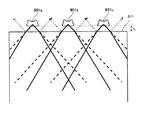
上述のように、携帯機器などに搭載される従来の液晶表示装置は、白色LEDと導光板との間、および白色LEDと樹脂フレームとの間にそれぞれ0.4mm前後の隙間があけられている。図11は、白色LEDと導光板との位置関係を示す模式図である。図11に示す白色LED901a〜901cと導光板911とは距離Lの隙間が生じるように離されて配置されている。この隙間は、落下衝撃による故障の発生を防ぐために有効である。しかし、白色LED901a〜901cから放射された光の導光板911に対する入射光量を低下させるため、光の利用効率を悪化させる要因となる。
【0011】
また、白色LED901a〜901cから放射された光は、隙間内の空気中を進んで導光板911の光入射面に達する。ここで、当該光の一部は、空気の屈折率とは異なる屈折率を有する導光板911の界面で反射されるため、導光板911に入射する光の光量には反射ロスが発生する。図11に示す実線は白色LED901a〜901cから放射された光線を例示し、太い破線は導光板911が存在しないと仮定する場合(または導光板911の屈折率が空気と同じであると仮定する場合)の光線を例示し、細い破線は導光板911の界面で反射された光線を例示している。このような反射光の発生による反射ロスは、光の利用効率を悪化させる要因となる。
【0012】
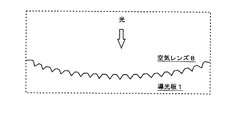
ここで、上述の特開2001−67917号公報に開示される構成のように白色LEDと導光板との隙間を樹脂で充填すれば、光の利用効率を向上させることができる。しかし、白色LEDからの光の放射角度が狭いため、白色LEDの放射角度内の領域外縁部に明線が発生する。この明線とは、本明細書中では導光板上に見かけ上生じる、明るい領域と暗い領域との境界線を指すものとする。図12は、この明線を例示する模式図である。白色LED901a〜901cの放射角度内の領域の光量はLEDの放射特性から決定されるが、当該放射角度外の領域の光量はかなり少ない。そのため、上記放射角度内の領域と放射角度外の領域との境界は明線として現れ、導光板上の輝度均一性を実現するにあたり障害となる。
【0013】
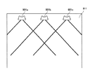
なお、隙間へ充填される樹脂材料を変更することによりその屈折率が導光板の屈折率よりもより大きくなるように調整すれば、上記LEDからの光の放射角度をLEDの放射特性に基づく放射角度より広げることができる。しかし、充填される樹脂材料と導光板との屈折率差が大きくなるほど反射ロスが増大する。図13は、白色LEDと導光板との隙間が導光板の屈折率よりもより大きい屈折率を有する樹脂で充填される場合のLEDからの光線の屈折態様を例示する模式図である。図13に示す実線、太い破線、および細い破線は図11の場合と同様のものを示しており、θはLEDの放射特性に基づく放射角度を示し、θ’はθより広げられたLEDからの光の放射角度を示す。この図13に示す反射光の発生による反射ロスは、光の利用効率を悪化させる要因となる。
【0014】
そこで、本発明の目的は、光源からの光の利用効率を向上させ、かつ導光板上の輝度均一性を実現する面状照明装置およびこれを使用した液晶表示装置を提供することである。
【0015】
【課題を解決するための手段】
第1の発明は、光源と、当該光源からの光を受け取る光入射面および受け取られた光を放つ光出射面を有する導光体とを備える面状照明装置であって、
前記光源と前記導光体の光入射面との間には、空気よりも大きい屈折率を有する所定の物質が充填され、
前記導光体は、他の部分とは異なる屈折率を有する屈折部を、前記光入射面近傍に含むことを特徴とする。
【0016】
このような第1の発明によれば、光源と導光体の光入射面との間に空気よりも大きい屈折率を有する物質が充填されることにより、導光体との屈折率差が小さくなるため光の反射ロスが低減される。また、導光体の入射面近傍の内部に屈折部を含むことにより、導光体の明るい領域が広くなり導光体上の輝度が均一となる。
【0017】
第2の発明は、第1の発明において、
前記屈折部は、空気からなることを特徴とする。
【0018】
このような第2の発明によれば、屈折部に特別な素材を充填する必要がないため、容易にまたは安価な構成で導光体の明るい領域が広くなり、導光体上の輝度が均一となる。
【0019】
第3の発明は、第1または第2の発明において、
前記屈折部は、前記光源からの光を屈折または発散することにより、当該光に照らされる前記導光体の明るい領域を広げるように構成されることを特徴とする。
【0020】
このような第3の発明によれば、屈折部により導光体の明るい領域が広がるため、導光体上の輝度が均一となる。
【0021】
第4の発明は、第1から第3までのいずれか1つの発明において、
前記屈折部は、光線を発散するレンズであることを特徴とする。
【0022】
このような第4の発明によれば、屈折部で光源からの光の放射角度が広げられることにより導光体の明るい領域が広くなり、導光体上の輝度が均一となる。
【0023】
第5の発明は、第1から第4までのいずれか1つの発明において、
前記導光体は、前記屈折部からの光を受け取る面で当該光を拡散するように構成されることを特徴とする。
【0024】
このような第5の発明によれば、上記面で光が拡散されるため、当該拡散された光により導光体上の輝度が均一となる。
【0025】
第6の発明は、第5の発明において、
前記屈折部からの光を受け取る面には、当該光を拡散するための起伏が設けられることを特徴とする。
【0026】
このような第6の発明によれば、当該起伏により、簡易な構成で光が拡散される。
【0027】
第7の発明は、第1の発明において、
前記光源は、前記導光体の所定の端面または当該端面近傍の内部に形成される収納空間内に配置され、
前記所定の物質は、前記光源が配置された収納空間内に充填されることを特徴とする。
【0028】
このような第7の発明によれば、光源が収納空間内に配置されるので、所定の充填すべき物質を簡易な工程で充填可能であり、また光の反射ロスが低減されるため光源からの光の利用効率が向上する。
【0029】
第8の発明は、第1または第7の発明において、
前記所定の物質は、弾力性を有することを特徴とする。
【0030】
このような第8の発明によれば、落下衝撃等による故障の発生が防止される。
【0031】
第9の発明は、第1の発明において、
前記所定の物質は、前記導光体の屈折率よりも大きい近傍値である所定の屈折率を有することを特徴とする。
【0032】
このような第9の発明によれば、光源からの光の放射角度が広げられつつ光の反射ロスが抑えられるため、導光体上の輝度が均一でありながら光の利用効率が向上する。
【0033】
第10の発明は、第1から第9までのいずれか1つの発明の面状照明装置を備えることを特徴とする、液晶表示装置である。
【0034】
【発明の実施の形態】
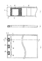
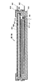
以下、添付図面を参照して本発明の一実施形態について説明する。本実施形態に係る液晶表示装置およびこれに用いられる面状照明装置の構造につき、図1を参照して説明する。図1は、本実施形態に係る液晶表示装置の導光板および光源近傍の構造例を示す図である。より詳細には、図1(a)は平面図であり、図1(b)は図1(a)に示すA−Aでの断面図であり、図1(c)は図1(b)の白色LED近傍を拡大した図である。
【0035】
この液晶表示装置は、光源である白色LED3a〜3cと、これらの光源からの光を所定面(照明面)から面状に放射する導光体としての導光板1と、筐体を構成する樹脂フレーム2と、半田付け部6で白色LED3a〜3cを半田付けされることによりこれらを実装するLED用FPC基板4と、反射シート5と、レンズシートや光拡散シート等からなる図示されないレンズシート類と、TFT基板およびCF基板からなる図示されない液晶パネルと、この液晶パネルからの信号を外部へ取り出すための図示されないパネル信号取出用FPC基板と、図示されない偏光板と、レンズシートや光拡散シート等からなるレンズシート類とを備える。図示されないこれらの構成要素は、図1に示す従来例とほぼ同様であるので、詳しい説明を省略する。また、導光板1および白色LED3a〜3cを主要な要素として面状照明装置(またはバックライト部)が構成される。この面状照明装置からの光の光量が液晶パネルの画素毎に適宜調節されることにより液晶表示装置の表示面に各種表示がなされる。
【0036】
樹脂フレーム2は、Pシャーシとも呼ばれており、例えば、光高反射グレードの帝人化成製パンライト(商標)LD−1000RMやLN−1000RMのようなポリカーボネート樹脂等からなる。
【0037】
導光板1には、例えば三菱エンジニアリングプラスティックス製アクリライトE(商標)のようなアクリル樹脂や、例えば出光石油化学製タフロン(商標)#1700のようなポリカーボネート樹脂を素材として使用する。なお、上記アクリライトE(商標)の屈折率(n)は1.19である(透過率はデータシートに記載なし)。また、上記タフロン(商標)#1700の屈折率(n)は1.585であり、透過率は85〜89%(3mm板厚)である。なお、この導光板1および樹脂フレーム2は、白色LED3a〜3cからの光束が導光板1の中へ効率よく入射されるのに適した厚さになるように設計される。
【0038】
図1(a)に示すように、導光板1は、白色LED3a〜3cが配置されるべき位置に相当する端部の一部分が直方体形状に欠けている。LED3a〜3cの配列に合わせてここでは3つの切り欠けが形成されているため、この導光板1の端部は櫛型様になっている。この切り欠け部分が白色LED3a〜3cを配置するための収納空間して機能する。白色LED3a〜3cは、周囲に隙間を生じるように、この切り欠け部分(収納空間)の適宜の位置に配置されており、この隙間には弾力性のある樹脂(以下「充填用樹脂」という)7が充填される。このことにより、白色LED3a〜3cからの光が導光板1へ効率良く入射され、かつ(落下衝撃等で)白色LED3a〜3cが導光板1や樹脂フレーム2と衝突することにより生じる白色LED3a〜3cの脱落や配線の切断などの故障の発生を未然に防止することができる。
【0039】
なお、上記収納空間は、必ずしも切り欠けである必要はなく、凹部であってもよい。例えば、収納空間は、表示面と反対側の導光板面が所定の厚さだけ残るように切り取られることにより、表示面側の導光板面が開口されており、表示面と反対側の導光板面が開口されない凹部であってもよい。
【0040】
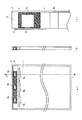
また、上記収納空間は、白色LED3a〜3cを収納する1つの切り欠けまたは凹部であってもよい。図2は、3つの白色LEDを収納するための(コの字状の)1つの収納空間を有する導光板および光源近傍の構造例を示す図である。より詳細には、図2(a)は平面図であり、図2(b)は図2(a)に示すB−Bでの断面図であり、図2(c)は図2(b)の白色LED近傍を拡大した図である。
【0041】
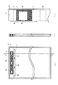
さらに、上記収納空間は、導光板1の端部近傍の内部(内側)に形成されてもよい。図3は、白色LEDを収納するための収納空間を内部に含む導光板および光源近傍の構造例を示す図である。より詳細には、図3(a)は平面図であり、図3(b)は図3(a)に示すC−Cでの断面図であり、図3(c)は図3(b)の白色LED近傍を拡大した図である。なお、上記収納空間は、貫通孔であっても凹部であってもよく、また、3つの白色LED3a〜3cに対応させて3つが設けられてもよい。
【0042】
以上のように、収納空間が形成されることにより、充填用樹脂7の充填が容易となる。また、導光板1の上記端部よりも内側に切り欠けや凹部などの収納空間が形成されることにより、収納空間の所定面(例えば白色LED3a〜3cからの光の放射方向にある面)で界面反射される光を収納空間の他の面(例えば上記所定面に垂直な面)から導光板1の内部に取り込むことができるため、白色LED3a〜3cからの光の反射ロスが低減され、当該光の利用効率が向上する。なお、当該光の利用効率をさらに向上させるために、白色LED3a〜3cの光の放射方向と反対側近傍に光を反射させるための反射部が設けられてもよい。この反射部は、ポリカーボネート板によって例えば白い壁状に形成されてもよいし、所定の曲面(例えばパラボラ形状の曲面)が形成され、当該曲面に光を反射するための反射シートが貼り付けられることにより形成されてもよい。この反射シートは、PET(ポリエチレンテレフタレート)シート、当該PETシートに銀がスパッタリングされた銀シート、またはポリエステル系樹脂の多層膜構造を有するESR(Enhanced Specular Reflector)シートなどである。
【0043】
上記収納空間に充填されるべき充填用樹脂7には、例えば、東芝GEシリコーン社製の高伸長・高強度シリコーンゲルTSE3062やTSE3070のようなポッティング(注型封止)用樹脂を使用する。なお、上記シリコーンゲルTSE3062およびTSE3070は、2成分室温硬化型のシリコーンポッティングゲルであって、その屈折率(n)は1.42であり、その透過率はほぼ80〜92%(10mm×10mm×45mmの容器に3gを入れて測定)である。また、その(特性からの)伸びは、上記TSE3062が150%、TSE3070が1500%であり、TSE3062が硬目である。これらはともに、A液とB液とを1対1の配合とし70℃で30分(室温では24時間程度)経過後、透明液状から柔らかい透明ゲル状に硬化する。これらの樹脂はともに、金属、プラスチック、セラミック、およびガラスなどに良く粘着する。そのため、衝撃や振動から部品(ここでは白色LED3a〜3c)が保護される。
【0044】
ここで、充填用樹脂7の材料を変更することによりその屈折率が導光板1の屈折率よりもより大きくなるように調整すれば、白色LED3a〜3cからの光の放射角度をLED3a〜3cの放射特性に基づく放射角度より広げることができる。しかし、充填用樹脂7と導光板1との屈折率差が大きくなるほど反射ロスが増大する。そのため、充填用樹脂7の屈折率は、空気の屈折率よりも大きく、かつ導光板1の屈折率よりも所定の範囲を超えて大きくなり過ぎないように調整されるのが好ましい。より好適には、導光板1の屈折率よりもやや大きい近傍の適宜の値に設定される。そうすれば、白色LED3a〜3cからの光の利用効率が向上する。
【0045】
以上のように充填用樹脂7の屈折率が導光板1の屈折率よりもそれほど大きくない場合(すなわち屈折率差が大きくない場合)には、白色LED3a〜3cからの光の放射角度をLED3a〜3cの放射特性に基づく放射角度より十分に広げることができない。
【0046】
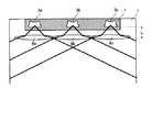
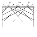
そこで、図1に示すように、白色LED3a〜3cが配置されるべき収納空間から適宜の距離があけられた位置の導光板1内に空気レンズ8a〜8cが設けられる。これらの空気レンズ8a〜8cは、白色LED3a〜3cから放射された(白色の)光線を屈折(ここでは発散)させるために設けられる。すなわちこの空気レンズ8a〜8cがない場合、面状照明装置の(表示面での)輝度均一性は白色LED3a〜3cの放射特性に依存する。そのため、白色LED3a〜3cからの光の放射角度が白色LED3a〜3cの放射特性に基づく放射角度よりも大きくなるように、白色LED3a近傍の導光板1中に空気レンズ8aが、白色LED3b近傍の導光板1中に空気レンズ8bが、白色LED3c近傍の導光板1中に空気レンズ8cがそれぞれ設けられる。
【0047】
なお、空気レンズ8a〜8cに代えて、空気の屈折率に近い樹脂材料が充填されて形成されるレンズを使用することも考えられるが、充填に適しており空気の屈折率に近い樹脂材料は実用上存在しない。もちろん、例えば風船のようなクッション状の材料を用いることも考えられるが、現実的ではない。また、充填用樹脂7の屈折率よりも導光板1の屈折率の方がより大きい場合、白色LED3a〜3cからの光の放射角度θ’は、白色LED3a〜3cの放射特性に基づく放射角度θよりも小さくなるので好適ではない。
【0048】
さらに、上記白色LED3a〜3cからの光線の屈折につき図4を参照して説明する。図4は、上記3つの空気レンズが設けられる場合の3つの白色LEDからの光線の屈折態様を示す模式図である。空気は導光板1の(材料の)屈折率よりも小さいため、図4に示される凸レンズ形状の空気レンズ8a〜8cにより光線が発散される。なお、空気中のガラス製凸レンズにより光線が収束されることに対して、この凸レンズは逆の作用を有している。また図中の距離Lは、各白色LED3a〜3cの光出射面から隣り合う白色LEDの明線の交差点までの、導光板1の長手方向に沿った距離である。この距離Lが短くなるほど、導光板1の明るい領域が広くなるため、面状照明装置の(表示面での)輝度均一性が十分に実現される。この距離Lは、白色LED3a〜3cの配置間隔が小さいほど(もしくは白色LEDの数を増やすほど)短くなり、また白色LED3a〜3cの放射角度が広いほど短くなる。さらに、この距離Lは、空気レンズ8a〜8cの厚み(形状)を変えることにより変更することができる。これらの空気レンズ8a〜8cにより、空気レンズが設けられない場合よりも距離Lが短くなり、輝度均一性が保たれる明るい領域の端部位置を白色LED3a〜3cに近づけることができる。
【0049】
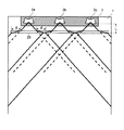
次に、空気レンズ8a〜8cにつき図5を参照して説明する。図5は、空気レンズの1つの形状を部分的に拡大して示す図である。図5では、白色LED3a〜3cからの光線は、導光板1を介して上方より空気レンズに入射される。図に示されるように、空気レンズからの光出射面すなわち空気レンズからの光線が再び入射される導光板1内部の所定面には起伏が形成されている。より詳細には、この起伏は、導光板1の厚み方向(表示面に対して垂直な方向)に沿って三角形状の断面を有する複数の溝、または断面が台形状である複数の突起部により形成される。この起伏により、導光板1へ再入射される光が拡散されるため、導光板1上の輝度均一性が実現される。なお、この起伏の形状は特に限定されるものではなく、例えばのこぎり状や不規則な形状の溝や突起であってもよい。また、レンズの上記光出射面には、光を拡散(散乱)するための拡散膜等が形成されてもよい。
【0050】
なお、上記一実施形態における空気レンズ8a〜8cは、1つの空気レンズであってもよく、また通常の凸レンズとは異なる形状の光を発散するレンズ(例えばシリンドリカルレンズ)であってもよい。図6は1つの空気レンズを含む導光板を示す模式図である。この空気レンズ18はシリンドリカルレンズであり、導光板1の厚み方向に曲率を有しない。導光板1の厚み方向への光の発散は必要ないからである。このシリンドリカルレンズは、通常の凸レンズと異なり厚み方向の断面形状が同一となるため、導光板1の成型が容易である。
【0051】
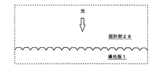
また、上記一実施形態における空気レンズ8a〜8cは光を発散するが、この空気レンズに代えて光を発散しない屈折部が備えられてもよい。図7は、空気レンズに代えて直方体形状の屈折部分を含む導光板と、白色LEDからの光線の屈折態様を示す模式図である。図に示すように、この屈折部28は自然に充填される空気からなる直方体の(レンズではない)形状であるため、白色LED3a〜3cからの光線を屈折するが発散しない。したがって、白色LED3a〜3cからの光の放射角度は変化しない。しかし、白色LED3a〜3cからの光線は屈折部28により屈折され、屈折部28がない場合の光線(図の破線)の位置より所定の距離だけ(図の左右方向に)ずれた位置から出射される。図中のdは、上記所定の距離を示す。このように光の放射位置が左右に広がるため、距離Lが短くなる。よって、導光板1の明るい領域が広くなるため、面状照明装置の(表示面での)輝度均一性が十分に実現される。
【0052】
さらに図5に示す空気レンズと同様に、上記屈折部28からの光出射面(すなわち屈折部から光線が再び入射される導光板1内部の所定面)には起伏が形成されてもよい。図8は、上記屈折部の形状を部分的に拡大して示す図である。なお、白色LED3a〜3cからの光線は、導光板1を介して図の上方より屈折部28に入射される。図8に示す起伏により、図5と同様に、導光板1へ再入射される光が拡散されるため、導光板1上の輝度均一性が実現される。なお、この起伏の形状は図5の場合と同様に限定されず、また上記光出射面には拡散膜等が形成されてもよい。
【0053】
このように、上記一実施形態における空気レンズ8a〜8cおよび屈折部28は、図の左右方向(導光板1の短手方向)に光を発散または屈折するものであればどのような形状であってもよい。また、空気レンズ8a〜8cまたは屈折部28には、導光板1周囲の空気が自然に充填されるが、この空気レンズ8a〜8cまたは屈折部28に代えて、導光板1の屈折率以下の屈折率を有する材料が用いられるレンズまたは屈折部が設けられてもよい。さらに、凸レンズである空気レンズ8a〜8cに代えて、導光板1の屈折率より大きい屈折率の材料が用いられる凹レンズ等が設けられてもよい。この場合にはこの凹レンズにより光線が発散される。
【0054】
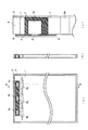
上記実施形態では、LED用FPC基板4と導光板1とが単に密着するが、これらを接着するために両面テープを用いるのが好適である。図9は、LED用FPC基板と導光板とが両面テープにより接着される液晶表示装置の構造例を示す図である。より詳細には、図9(a)は平面図であり、図9(b)は図9(a)に示すD−Dでの断面図であり、図9(c)は図9(b)の白色LED近傍を拡大した図である。これらの図を参照して、充填用樹脂7の充填作業を含む装置の組み立て手順例の一部を説明する。まず、樹脂フレーム2内に導光板1が組み込まれる。次に、白色LED3a〜3cが半田付け部6で半田付けされたLED用FPC基板4を、白色LED3a〜3cが収納空間に収納されるように、両面テープ9により導光板1に対して貼り付ける。最後に、LED用FPC基板4に半田付けされた白色LED3a〜3cが上になるように載置された後、収納空間に弾力性のある充填用樹脂7が注入され、常温(25℃)または高温(60℃程度)で硬化させられる。このような手順により、上記実施形態の液晶表示装置を容易に組み立てることができる。
【0055】
【発明の効果】
第1の発明によれば、光源と導光体の光入射面との間に空気よりも大きい屈折率を有する物質が充填されることにより、導光体との屈折率差が小さくなる。そのため光の反射ロスを低減し光源からの光の利用効率を向上させた面状照明装置を提供することができる。また、導光体の入射面近傍の内部に屈折部を含むことにより、導光体の明るい領域を広くし、導光体上の輝度均一性を実現する面状照明装置を提供することができる。
【0056】
第2の発明によれば、屈折部が空気からなるので、屈折部に特別な素材を充填する必要がない。そのため、容易にまたは安価に導光体の明るい領域を広くし、導光体上の輝度均一性を実現する面状照明装置を提供することができる。
【0057】
第3の発明によれば、屈折部により導光体の明るい領域が広がるため、導光体上の輝度均一性を実現する面状照明装置を提供することができる。
【0058】
第4の発明によれば、屈折部が光線を発散するレンズであるため、光源からの光の放射角度を広げることにより導光体の明るい領域を広くし、導光体上の輝度均一性を実現する面状照明装置を提供することができる。
【0059】
第5の発明によれば、導光体内部の前記屈折部からの光を受け取る面で光が拡散されるため、当該拡散された光により導光体上の輝度均一性を実現する面状照明装置を提供することができる。
【0060】
第6の発明によれば、屈折部からの光を受け取る面に起伏を設けることにより、簡易な構成で光を拡散させることができる。
【0061】
第7の発明によれば、光源が導光体の所定の端面または端面近傍の内部の収納空間内に配置されるので、所定の充填すべき物質を簡易な工程で充填することができ、また光の反射ロスが低減されるため光源からの光の利用効率を向上させた面状照明装置を提供することができる。
【0062】
第8の発明によれば、所定の物質が弾力性を有するため、落下衝撃等による故障の発生を防止することができる。
【0063】
第9の発明によれば、前記所定の物質が適宜の屈折率を有するように調整されるため、光源からの光の放射角度を広げつつ光の反射ロスを抑えることができる。よって導光体上の輝度均一性を実現しつつ光の利用効率を向上させる面状照明装置を提供することができる。
【0064】
第10の発明によれば、上記第1から第9までの発明に係る面状照明装置が使用される液晶表示装置を提供することができる。
【図面の簡単な説明】
【図1】本発明の一本実施形態に係る液晶表示装置の導光板および光源近傍の構造例を示す図である。
【図2】上記実施形態における3つの白色LEDを収納するための1つの収納空間を有する導光板および光源近傍の構造例を示す図である。
【図3】上記実施形態における白色LEDを収納するための収納空間を内部に含む導光板および光源近傍の構造例を示す図である。
【図4】上記実施形態における3つの空気レンズが設けられる場合の3つの白色LEDからの光線の屈折態様を示す模式図である。
【図5】上記実施形態における空気レンズの1つの形状を部分的に拡大して示す図である。
【図6】上記実施形態におけるシリンドリカルレンズである空気レンズを含む導光板を示す模式図である。
【図7】上記実施形態における直方体形状の屈折部を含む導光板と、白色LEDからの光線の屈折態様とを示す模式図である。
【図8】上記実施形態における屈折部の形状を部分的に拡大して示す図である
【図9】上記実施形態におけるLED用FPC基板と導光板とが両面テープにより接着される液晶表示装置の構造例を示す図である。
【図10】従来の面状照明装置を含む液晶表示装置の構成を示す側面概略図である。
【図11】従来の面状照明装置における白色LEDと導光板との位置関係を示す模式図である。
【図12】従来の面状照明装置における導光板上に見かけ上生じる明線を例示する模式図である。
【図13】従来の面状照明装置における白色LEDと導光板との隙間が樹脂で充填される場合のLEDからの光線の屈折態様を例示する模式図である。
【符号の説明】
1 …導光板
2 …樹脂フレーム
3a〜3c …白色LED
4 …LED用FPC基板
5 …反射シート
6 …半田付け部
7 …充填用樹脂
8a〜8c …空気レンズ
9 …両面テープ
18 …空気レンズ
28 …屈折部[0001]
TECHNICAL FIELD OF THE INVENTION
The present invention relates to a planar lighting device and a liquid crystal display device using the same, and more particularly, to a planar lighting device including a light guide (light guide plate) into which light from a light source is incident, and a liquid crystal display device using the same. .
[0002]
[Prior art]
2. Description of the Related Art In recent years, there has been a strong demand for miniaturization of liquid crystal applied products such as mobile phones, and with this demand, there has been a demand for miniaturization and thinning of a liquid crystal display device and a planar lighting device used therein. Such a conventional planar lighting device is provided with a light source such as a white light emitting diode (LED) or a cold cathode fluorescent tube (CCFT) at a certain distance from the light source. A light guide plate provided (via air), and the light from the light source is incident on a predetermined light incident surface of the light guide plate, and then diffused throughout the light guide plate to thereby provide a predetermined surface (illumination surface). ) Is radiated in a planar manner.
[0003]
FIG. 10 is a schematic side view showing the configuration of a liquid crystal display device including such a conventional planar illumination device. This liquid crystal display device includes a white LED 901 as a light source, an FPC (Flexible Printed Circuit)
[0004]
The
[0005]
The white LED 901 is installed with a space from the light incident surface of the
[0006]
The light emitted from the white LED 901 is three-dimensional radiation having a predetermined solid angle, and reflection occurs because the light incident surface of the
[0007]
Further, in the conventional configuration, a flat or wedge-shaped light guide plate having a thickness of 0.7 mm to 1 mm changes incident light from the white LED in the horizontal direction (parallel to the display surface) by 90 degrees to the display surface. Since a loss occurs when the light is emitted, it is necessary to further increase the light incidence efficiency on the light incident surface.
[0008]
In this regard, JP-A-2001-67917 discloses a configuration in which the light guide is integrated with the LED to improve the light use efficiency of the LED. A configuration is disclosed in which a slit is formed between a light incident surface and a light exit surface of a light guide plate to reduce luminance unevenness in a display area.
[0009]
[Patent Document 1]
JP-A-11-184386
[Patent Document 2]
JP-A-2001-67917
[Patent Document 3]
JP-A-2002-184225
[0010]
[Problems to be solved by the invention]
As described above, the conventional liquid crystal display device mounted on a portable device or the like has a gap of about 0.4 mm between the white LED and the light guide plate and between the white LED and the resin frame. . FIG. 11 is a schematic diagram illustrating a positional relationship between the white LED and the light guide plate. The
[0011]
Light emitted from the
[0012]
Here, if the gap between the white LED and the light guide plate is filled with resin as in the configuration disclosed in the above-mentioned Japanese Patent Application Laid-Open No. 2001-67917, the light use efficiency can be improved. However, since the emission angle of the light from the white LED is narrow, a bright line is generated at the outer edge of the area within the emission angle of the white LED. In the present specification, the bright line indicates a boundary line between a bright region and a dark region that appears on the light guide plate. FIG. 12 is a schematic view illustrating this bright line. The light amount in the area within the emission angle of the
[0013]
If the refractive index of the light guide plate is adjusted to be larger than the refractive index of the light guide plate by changing the resin material filled in the gap, the emission angle of the light from the LED can be changed based on the emission characteristics of the LED. Can be wider than the angle. However, as the refractive index difference between the resin material to be filled and the light guide plate increases, the reflection loss increases. FIG. 13 is a schematic diagram illustrating a refraction mode of a light beam from an LED when a gap between the white LED and the light guide plate is filled with a resin having a refractive index larger than that of the light guide plate. The solid line, the thick broken line, and the thin broken line shown in FIG. 13 indicate the same as in FIG. 11, where θ indicates the emission angle based on the emission characteristics of the LED, and θ ′ indicates the emission angle from the LED wider than θ. Indicates the light emission angle. The reflection loss due to the generation of the reflected light shown in FIG. 13 is a factor that deteriorates the light use efficiency.
[0014]
Therefore, an object of the present invention is to provide a planar illumination device that improves the efficiency of using light from a light source and realizes uniformity of luminance on a light guide plate, and a liquid crystal display device using the same.
[0015]
[Means for Solving the Problems]
A first invention is a spread illuminating device including a light source, and a light guide having a light incident surface that receives light from the light source and a light emitting surface that emits the received light,
A predetermined substance having a refractive index higher than that of air is filled between the light source and the light incident surface of the light guide,
The light guide includes a refraction portion having a different refractive index from other portions in the vicinity of the light incident surface.
[0016]
According to the first aspect, the substance having a refractive index larger than that of air is filled between the light source and the light incident surface of the light guide, so that the difference in the refractive index between the light guide and the light guide is small. Therefore, the reflection loss of light is reduced. In addition, since the light guide includes the refraction portion in the vicinity of the incident surface, the bright region of the light guide is widened and the brightness on the light guide becomes uniform.
[0017]
In a second aspect, in the first aspect,
The refracting portion is made of air.
[0018]
According to the second aspect, it is not necessary to fill the refraction portion with a special material. Therefore, the bright region of the light guide is widened with an easy or inexpensive configuration, and the brightness on the light guide is uniform. It becomes.
[0019]
A third invention is a method according to the first or second invention,
The refraction unit is configured to refract or diverge light from the light source, thereby expanding a bright region of the light guide illuminated by the light.
[0020]
According to the third aspect, the bright region of the light guide is widened by the refraction portion, so that the brightness on the light guide becomes uniform.
[0021]
According to a fourth aspect, in any one of the first to third aspects,
The refraction unit is a lens that diverges light rays.
[0022]
According to the fourth aspect of the invention, the light emission angle of the light source is widened by the refraction portion, so that the bright region of the light guide is widened and the brightness on the light guide is uniform.
[0023]
According to a fifth aspect, in any one of the first to fourth aspects,
The light guide is configured to diffuse the light on a surface that receives the light from the refraction unit.
[0024]
According to the fifth aspect, since the light is diffused on the surface, the luminance on the light guide becomes uniform by the diffused light.
[0025]
According to a sixth aspect, in the fifth aspect,
The surface for receiving the light from the refraction portion is provided with undulations for diffusing the light.
[0026]
According to the sixth aspect, the undulation diffuses light with a simple configuration.
[0027]
According to a seventh aspect, in the first aspect,
The light source is disposed in a storage space formed inside a predetermined end surface of the light guide or near the end surface,
The predetermined material may be filled in a storage space where the light source is disposed.
[0028]
According to the seventh aspect, since the light source is disposed in the storage space, the predetermined substance to be filled can be filled in a simple process, and the reflection loss of light is reduced. Light utilization efficiency is improved.
[0029]
In an eighth aspect based on the first or seventh aspect,
The predetermined substance has elasticity.
[0030]
According to the eighth aspect, occurrence of a failure due to a drop impact or the like is prevented.
[0031]
The ninth invention is based on the first invention,
The predetermined substance has a predetermined refractive index that is a near value larger than the refractive index of the light guide.
[0032]
According to the ninth aspect, since the reflection loss of light is suppressed while the radiation angle of light from the light source is widened, the light use efficiency is improved while the luminance on the light guide is uniform.
[0033]
A tenth invention is a liquid crystal display device comprising the planar lighting device of any one of the first to ninth inventions.
[0034]
BEST MODE FOR CARRYING OUT THE INVENTION
Hereinafter, an embodiment of the present invention will be described with reference to the accompanying drawings. The structure of the liquid crystal display device according to the present embodiment and the planar lighting device used for the same will be described with reference to FIG. FIG. 1 is a diagram illustrating an example of a structure near a light guide plate and a light source of a liquid crystal display device according to the present embodiment. More specifically, FIG. 1A is a plan view, FIG. 1B is a cross-sectional view taken along AA shown in FIG. 1A, and FIG. 1C is FIG. FIG. 4 is an enlarged view of the vicinity of a white LED.
[0035]
This liquid crystal display device includes
[0036]
The
[0037]
The
[0038]
As shown in FIG. 1A, the
[0039]
Note that the storage space does not necessarily have to be a notch, but may be a recess. For example, the storage space is cut out so that the light guide plate surface on the opposite side to the display surface remains a predetermined thickness, so that the light guide plate surface on the display surface side is opened, and the light guide plate on the opposite side to the display surface is opened. It may be a concave part whose surface is not opened.
[0040]
Further, the storage space may be a single cutout or a recess for storing the
[0041]
Further, the storage space may be formed inside (inside) near the end of the
[0042]
As described above, by forming the storage space, the filling of the filling
[0043]
As the filling
[0044]
Here, if the refractive index of the filling
[0045]
As described above, when the refractive index of the filling
[0046]
Therefore, as shown in FIG. 1, the
[0047]
In addition, instead of the
[0048]
Further, the refraction of light rays from the
[0049]
Next, the
[0050]
The
[0051]
In addition, the
[0052]
Further, similarly to the air lens shown in FIG. 5, an undulation may be formed on the light exit surface from the refraction portion 28 (that is, a predetermined surface inside the
[0053]
As described above, the
[0054]
In the above embodiment, the
[0055]
【The invention's effect】
According to the first invention, the difference between the refractive index of the light guide and that of the light guide is reduced by filling the space between the light source and the light incident surface of the light guide with a substance having a refractive index higher than that of air. Therefore, it is possible to provide a spread illuminating device in which the reflection loss of light is reduced and the use efficiency of light from the light source is improved. In addition, by including a refraction portion inside the vicinity of the incident surface of the light guide, it is possible to provide a spread illuminating device that widens a bright region of the light guide and realizes uniform brightness on the light guide. .
[0056]
According to the second aspect, since the bending portion is made of air, it is not necessary to fill the bending portion with a special material. Therefore, it is possible to provide a spread illuminating device that easily or inexpensively enlarges the bright area of the light guide and realizes uniform brightness on the light guide.
[0057]
According to the third aspect, since the bright region of the light guide is expanded by the refraction portion, it is possible to provide a spread illuminating device that realizes uniform brightness on the light guide.
[0058]
According to the fourth aspect, since the refracting portion is a lens that diverges light rays, the bright area of the light guide is widened by widening the emission angle of light from the light source, and the brightness uniformity on the light guide is improved. A surface illumination device that can be realized can be provided.
[0059]
According to the fifth aspect, since the light is diffused on the surface of the light guide that receives the light from the refraction portion, the spread light achieves the uniformity of the brightness on the light guide by the diffused light. An apparatus can be provided.
[0060]
According to the sixth aspect, the unevenness is provided on the surface for receiving the light from the refraction portion, so that the light can be diffused with a simple configuration.
[0061]
According to the seventh aspect, since the light source is disposed in the internal storage space at or near the predetermined end face of the light guide, the predetermined substance to be filled can be filled in a simple process. Since the reflection loss of light is reduced, it is possible to provide a spread illuminating device in which the use efficiency of light from a light source is improved.
[0062]
According to the eighth aspect, since the predetermined substance has elasticity, occurrence of a failure due to a drop impact or the like can be prevented.
[0063]
According to the ninth aspect, since the predetermined substance is adjusted to have an appropriate refractive index, it is possible to suppress the reflection loss of light while widening the radiation angle of light from the light source. Therefore, it is possible to provide a spread illuminating device that improves the light use efficiency while realizing the luminance uniformity on the light guide.
[0064]
According to the tenth aspect, it is possible to provide a liquid crystal display device using the planar lighting device according to the first to ninth aspects.
[Brief description of the drawings]
FIG. 1 is a diagram showing a structural example near a light guide plate and a light source of a liquid crystal display device according to an embodiment of the present invention.
FIG. 2 is a diagram showing an example of a structure near a light source and a light guide plate having one storage space for storing three white LEDs in the embodiment.
FIG. 3 is a diagram showing an example of a structure near a light source and a light guide plate including a storage space for storing a white LED in the embodiment.
FIG. 4 is a schematic diagram showing a refraction mode of light rays from three white LEDs when three air lenses are provided in the embodiment.
FIG. 5 is a partially enlarged view showing one shape of the air lens in the embodiment.
FIG. 6 is a schematic view showing a light guide plate including an air lens which is a cylindrical lens in the embodiment.
FIG. 7 is a schematic diagram showing a light guide plate including a rectangular parallelepiped refraction portion in the embodiment and a refraction mode of a light beam from a white LED.
FIG. 8 is a diagram showing a partially enlarged shape of a bending portion in the embodiment.
FIG. 9 is a diagram showing a structural example of a liquid crystal display device in which the LED FPC board and the light guide plate in the embodiment are adhered with a double-sided tape.
FIG. 10 is a schematic side view showing a configuration of a liquid crystal display device including a conventional planar illumination device.
FIG. 11 is a schematic diagram showing a positional relationship between a white LED and a light guide plate in a conventional planar lighting device.
FIG. 12 is a schematic view illustrating a bright line apparently generated on a light guide plate in a conventional planar lighting device.
FIG. 13 is a schematic view illustrating a mode of refraction of a light beam from an LED when a gap between a white LED and a light guide plate in a conventional planar illumination device is filled with a resin.
[Explanation of symbols]
1 ... light guide plate
2 ... resin frame
3a to 3c: White LED
4… FPC board for LED
5… Reflective sheet
6… Soldering part
7 ... Filling resin
8a-8c ... air lens
9 Double-sided tape
18 ... air lens
28 ... refraction part
Claims (10)
前記光源と前記導光体の光入射面との間には、空気よりも大きい屈折率を有する所定の物質が充填され、
前記導光体は、他の部分とは異なる屈折率を有する屈折部を、前記光入射面近傍に含むことを特徴とする、面状照明装置。A planar illumination device including a light source and a light guide having a light incident surface that receives light from the light source and a light emission surface that emits the received light,
A predetermined substance having a refractive index higher than that of air is filled between the light source and the light incident surface of the light guide,
The planar light device, wherein the light guide includes a refraction portion having a different refractive index from other portions near the light incident surface.
前記所定の物質は、前記光源が配置された収納空間内に充填されることを特徴とする、請求項1に記載の面状照明装置。The light source is disposed in a storage space formed inside a predetermined end surface of the light guide or near the end surface,
The planar lighting device according to claim 1, wherein the predetermined material is filled in a storage space where the light source is disposed.
Priority Applications (1)
| Application Number | Priority Date | Filing Date | Title |
|---|---|---|---|
| JP2003028498A JP2004241237A (en) | 2003-02-05 | 2003-02-05 | Surface illumination device and liquid crystal display device using the same |
Applications Claiming Priority (1)
| Application Number | Priority Date | Filing Date | Title |
|---|---|---|---|
| JP2003028498A JP2004241237A (en) | 2003-02-05 | 2003-02-05 | Surface illumination device and liquid crystal display device using the same |
Publications (1)
| Publication Number | Publication Date |
|---|---|
| JP2004241237A true JP2004241237A (en) | 2004-08-26 |
Family
ID=32955954
Family Applications (1)
| Application Number | Title | Priority Date | Filing Date |
|---|---|---|---|
| JP2003028498A Pending JP2004241237A (en) | 2003-02-05 | 2003-02-05 | Surface illumination device and liquid crystal display device using the same |
Country Status (1)
| Country | Link |
|---|---|
| JP (1) | JP2004241237A (en) |
Cited By (24)
| Publication number | Priority date | Publication date | Assignee | Title |
|---|---|---|---|---|
| WO2006045142A1 (en) * | 2004-10-25 | 2006-05-04 | Rpo Pty Limited | Planar lenses for integrated optics |
| KR100754382B1 (en) * | 2006-01-20 | 2007-08-31 | 삼성전기주식회사 | Backlight unit |
| US7314302B2 (en) | 2005-01-03 | 2008-01-01 | Samsung Electronics Co., Ltd. | Backlight assembly removing dark areas and display device provided with the same |
| JPWO2007083805A1 (en) * | 2006-01-23 | 2009-06-18 | 富士フイルム株式会社 | Surface lighting device |
| US7695178B2 (en) | 2005-06-23 | 2010-04-13 | Samsung Electronics Co., Ltd | Light-guide plate, backlight assembly and liquid crystal display having the same |
| US7826703B2 (en) | 2005-08-17 | 2010-11-02 | Fujifilm Corporation | Planar illuminating device |
| WO2012030085A1 (en) * | 2010-09-03 | 2012-03-08 | Lg Innotek Co., Ltd. | Backlight unit and method for manufacturing the same |
| WO2012030084A1 (en) * | 2010-08-31 | 2012-03-08 | Lg Innotek Co., Ltd. | Backlight unit |
| WO2012067340A1 (en) * | 2010-11-15 | 2012-05-24 | Lg Innotek Co., Ltd. | Backlight unit |
| JP2012104312A (en) * | 2010-11-09 | 2012-05-31 | Alps Electric Co Ltd | Illumination device and method of manufacturing the same |
| WO2012070765A1 (en) * | 2010-11-22 | 2012-05-31 | Lg Innotek Co., Ltd. | Method for manufacturing backlight unit |
| JP2012150429A (en) * | 2011-01-19 | 2012-08-09 | Samsung Electronics Co Ltd | Display device |
| KR101211717B1 (en) | 2010-11-15 | 2012-12-12 | 엘지이노텍 주식회사 | Back Light Unit within Rasin or Optical pattern |
| KR101211711B1 (en) * | 2010-11-15 | 2012-12-18 | 엘지이노텍 주식회사 | Back Light Unit within Rasin |
| TWI396016B (en) * | 2008-12-30 | 2013-05-11 | Innolux Corp | Backlight module which increases optics energy utility rate and lcd having the same |
| KR101264675B1 (en) * | 2005-09-01 | 2013-05-16 | 엘지디스플레이 주식회사 | Backlight unit using a test device for testing of LCD Panel |
| KR101331908B1 (en) * | 2012-07-04 | 2013-11-22 | 엘지디스플레이 주식회사 | Backlight unit for liquid crystal display device and method of fabricating thereof |
| JP2013545247A (en) * | 2010-12-04 | 2013-12-19 | スリーエム イノベイティブ プロパティズ カンパニー | Lighting assembly and method of forming the same |
| JP2016540359A (en) * | 2013-12-13 | 2016-12-22 | ヴァレオ システム テルミク | Lighting device |
| WO2017122794A1 (en) * | 2016-01-15 | 2017-07-20 | シチズン電子株式会社 | Planar light unit |
| JP2019105827A (en) * | 2017-12-12 | 2019-06-27 | 現代自動車株式会社Hyundai Motor Company | Optical diffusion compound lens |
| WO2020153430A1 (en) * | 2019-01-25 | 2020-07-30 | ファイバーテック株式会社 | Optical probe |
| CN111538116A (en) * | 2020-05-15 | 2020-08-14 | 惠州迈特光电科技有限公司 | Self-diffusion light guide plate and manufacturing process thereof |
| WO2022009653A1 (en) * | 2020-07-09 | 2022-01-13 | 東レ株式会社 | Plastic optical fiber, medical lighting device, medical sensor device, medical phototherapeutic device, and plastic optical fiber cord |
-
2003
- 2003-02-05 JP JP2003028498A patent/JP2004241237A/en active Pending
Cited By (41)
| Publication number | Priority date | Publication date | Assignee | Title |
|---|---|---|---|---|
| WO2006045142A1 (en) * | 2004-10-25 | 2006-05-04 | Rpo Pty Limited | Planar lenses for integrated optics |
| US7314302B2 (en) | 2005-01-03 | 2008-01-01 | Samsung Electronics Co., Ltd. | Backlight assembly removing dark areas and display device provided with the same |
| US7695178B2 (en) | 2005-06-23 | 2010-04-13 | Samsung Electronics Co., Ltd | Light-guide plate, backlight assembly and liquid crystal display having the same |
| US7826703B2 (en) | 2005-08-17 | 2010-11-02 | Fujifilm Corporation | Planar illuminating device |
| KR101264675B1 (en) * | 2005-09-01 | 2013-05-16 | 엘지디스플레이 주식회사 | Backlight unit using a test device for testing of LCD Panel |
| KR100754382B1 (en) * | 2006-01-20 | 2007-08-31 | 삼성전기주식회사 | Backlight unit |
| US7901125B2 (en) | 2006-01-23 | 2011-03-08 | Fujifilm Corporation | Wedge-shaped lighting device |
| JP4709230B2 (en) * | 2006-01-23 | 2011-06-22 | 富士フイルム株式会社 | Surface lighting device |
| JPWO2007083805A1 (en) * | 2006-01-23 | 2009-06-18 | 富士フイルム株式会社 | Surface lighting device |
| TWI396016B (en) * | 2008-12-30 | 2013-05-11 | Innolux Corp | Backlight module which increases optics energy utility rate and lcd having the same |
| WO2012030084A1 (en) * | 2010-08-31 | 2012-03-08 | Lg Innotek Co., Ltd. | Backlight unit |
| TWI509323B (en) * | 2010-08-31 | 2015-11-21 | Lg Innotek Co Ltd | Backlight unit |
| WO2012030085A1 (en) * | 2010-09-03 | 2012-03-08 | Lg Innotek Co., Ltd. | Backlight unit and method for manufacturing the same |
| JP2012104312A (en) * | 2010-11-09 | 2012-05-31 | Alps Electric Co Ltd | Illumination device and method of manufacturing the same |
| WO2012067340A1 (en) * | 2010-11-15 | 2012-05-24 | Lg Innotek Co., Ltd. | Backlight unit |
| KR101211711B1 (en) * | 2010-11-15 | 2012-12-18 | 엘지이노텍 주식회사 | Back Light Unit within Rasin |
| KR101211717B1 (en) | 2010-11-15 | 2012-12-12 | 엘지이노텍 주식회사 | Back Light Unit within Rasin or Optical pattern |
| CN103210342B (en) * | 2010-11-15 | 2016-10-05 | Lg伊诺特有限公司 | Back light unit |
| US9625642B2 (en) | 2010-11-15 | 2017-04-18 | Lg Innotek Co., Ltd. | Light unit |
| CN103210342A (en) * | 2010-11-15 | 2013-07-17 | Lg伊诺特有限公司 | Backlight unit |
| TWI494658B (en) * | 2010-11-15 | 2015-08-01 | Lg Innotek Co Ltd | Light emitting device |
| WO2012070765A1 (en) * | 2010-11-22 | 2012-05-31 | Lg Innotek Co., Ltd. | Method for manufacturing backlight unit |
| KR101279471B1 (en) | 2010-11-22 | 2013-06-27 | 엘지이노텍 주식회사 | Manufacturing method of backlight unit |
| JP2013545247A (en) * | 2010-12-04 | 2013-12-19 | スリーエム イノベイティブ プロパティズ カンパニー | Lighting assembly and method of forming the same |
| US9217895B2 (en) | 2011-01-19 | 2015-12-22 | Samsung Display Co., Ltd. | Display apparatus |
| JP2012150429A (en) * | 2011-01-19 | 2012-08-09 | Samsung Electronics Co Ltd | Display device |
| KR101331908B1 (en) * | 2012-07-04 | 2013-11-22 | 엘지디스플레이 주식회사 | Backlight unit for liquid crystal display device and method of fabricating thereof |
| JP2016540359A (en) * | 2013-12-13 | 2016-12-22 | ヴァレオ システム テルミク | Lighting device |
| WO2017122794A1 (en) * | 2016-01-15 | 2017-07-20 | シチズン電子株式会社 | Planar light unit |
| JPWO2017122794A1 (en) * | 2016-01-15 | 2018-11-08 | シチズン電子株式会社 | Surface light unit |
| US10591662B2 (en) | 2016-01-15 | 2020-03-17 | Citizen Electronics Co., Ltd. | Planar light unit |
| JP7262963B2 (en) | 2017-12-12 | 2023-04-24 | 現代自動車株式会社 | light diffusing compound lens |
| JP2019105827A (en) * | 2017-12-12 | 2019-06-27 | 現代自動車株式会社Hyundai Motor Company | Optical diffusion compound lens |
| WO2020153430A1 (en) * | 2019-01-25 | 2020-07-30 | ファイバーテック株式会社 | Optical probe |
| JPWO2020153430A1 (en) * | 2019-01-25 | 2021-12-02 | ファイバーテック株式会社 | Optical probe |
| CN111538116A (en) * | 2020-05-15 | 2020-08-14 | 惠州迈特光电科技有限公司 | Self-diffusion light guide plate and manufacturing process thereof |
| CN111538116B (en) * | 2020-05-15 | 2022-08-30 | 上海精见新材料有限公司 | Self-diffusion light guide plate and manufacturing process thereof |
| JPWO2022009653A1 (en) * | 2020-07-09 | 2022-01-13 | ||
| WO2022009653A1 (en) * | 2020-07-09 | 2022-01-13 | 東レ株式会社 | Plastic optical fiber, medical lighting device, medical sensor device, medical phototherapeutic device, and plastic optical fiber cord |
| US12449587B2 (en) | 2020-07-09 | 2025-10-21 | Toray Industries, Inc. | Plastic optical fiber, medical lighting device, medical sensor device, medical phototherapy device, and plastic optical fiber cord |
| JP7764761B2 (en) | 2020-07-09 | 2025-11-06 | 東レ株式会社 | Plastic optical fibers, medical lighting equipment, medical sensor equipment, medical phototherapy equipment, and plastic optical fiber cords |
Similar Documents
| Publication | Publication Date | Title |
|---|---|---|
| JP2004241237A (en) | Surface illumination device and liquid crystal display device using the same | |
| US7360937B2 (en) | White light generating unit, backlight assembly having the same and liquid crystal display device having the same | |
| US11092847B2 (en) | Backlight module and display device | |
| US10302837B2 (en) | Backlight unit and liquid crystal display including the same | |
| JP4156919B2 (en) | Planar light source device, liquid crystal display device, and display device | |
| US9477117B2 (en) | Optical lens module and backlight unit | |
| US7658502B2 (en) | Back light structure of liquid crystal display device | |
| WO2012057017A1 (en) | Lighting device and display device | |
| KR100814559B1 (en) | Backlight device and liquid crystal apparatus | |
| KR20070120480A (en) | Liquid crystal display | |
| KR20210025308A (en) | Display device having glass diffuser plast | |
| US7226200B2 (en) | Light guiding device with two opposite light emitting surfaces and backlight module using the same | |
| US20210215965A1 (en) | Display device | |
| US20170059764A1 (en) | Light guide plate, backlight unit and display device | |
| US11402690B2 (en) | Backlight unit and liquid crystal display device including the same | |
| US20070047219A1 (en) | Direct-lit backlight having light sources with bifunctional diverters | |
| US6474824B1 (en) | Surface-emitting device, front light, and liquid crystal device | |
| RU2504810C1 (en) | Liquid crystal display device | |
| JP2013218826A (en) | Light source device, planar light source device, display device, and lighting device | |
| CN113156707A (en) | Surface light source device and flat panel display device | |
| JP2015035252A (en) | Light source device, surface light source device, display device, and lighting device | |
| JP2001093315A (en) | Lighting device and display device | |
| JP2003162915A (en) | Surface light emitter and liquid crystal display device | |
| JP3988801B2 (en) | Surface light source device | |
| KR20060093956A (en) | Backlight unit of liquid crystal display device having integral reflection member |