EP1938241B1 - Vorrichtung zur erkennung der datenübertragungsrichtung zwischen kommunikationspartnern - Google Patents
Vorrichtung zur erkennung der datenübertragungsrichtung zwischen kommunikationspartnern Download PDFInfo
- Publication number
- EP1938241B1 EP1938241B1 EP06791376A EP06791376A EP1938241B1 EP 1938241 B1 EP1938241 B1 EP 1938241B1 EP 06791376 A EP06791376 A EP 06791376A EP 06791376 A EP06791376 A EP 06791376A EP 1938241 B1 EP1938241 B1 EP 1938241B1
- Authority
- EP
- European Patent Office
- Prior art keywords
- signal
- fact
- measuring circuit
- amax
- data transmission
- Prior art date
- Legal status (The legal status is an assumption and is not a legal conclusion. Google has not performed a legal analysis and makes no representation as to the accuracy of the status listed.)
- Not-in-force
Links
Images

Classifications
-
- G—PHYSICS
- G06—COMPUTING OR CALCULATING; COUNTING
- G06K—GRAPHICAL DATA READING; PRESENTATION OF DATA; RECORD CARRIERS; HANDLING RECORD CARRIERS
- G06K7/00—Methods or arrangements for sensing record carriers, e.g. for reading patterns
- G06K7/0013—Methods or arrangements for sensing record carriers, e.g. for reading patterns by galvanic contacts, e.g. card connectors for ISO-7816 compliant smart cards or memory cards, e.g. SD card readers
-
- G—PHYSICS
- G06—COMPUTING OR CALCULATING; COUNTING
- G06K—GRAPHICAL DATA READING; PRESENTATION OF DATA; RECORD CARRIERS; HANDLING RECORD CARRIERS
- G06K7/00—Methods or arrangements for sensing record carriers, e.g. for reading patterns
- G06K7/0013—Methods or arrangements for sensing record carriers, e.g. for reading patterns by galvanic contacts, e.g. card connectors for ISO-7816 compliant smart cards or memory cards, e.g. SD card readers
- G06K7/0086—Methods or arrangements for sensing record carriers, e.g. for reading patterns by galvanic contacts, e.g. card connectors for ISO-7816 compliant smart cards or memory cards, e.g. SD card readers the connector comprising a circuit for steering the operations of the card connector
Definitions
- the invention relates to a device for detecting the data transmission direction between two communication units according to the preamble of patent claim 1.
- a device for detecting the data transmission direction between a data carrier and a data carrier reading unit which has a measuring circuit.
- the measuring circuit is between the input / output terminal (I / O terminal) of the data carrier and the input / output terminal (I / O terminal) of the disk reading unit connected to each other by means of a connection line (I / O line) are connected, arranged.
- the measuring circuit is constructed in the manner of a bridge circuit, wherein two voltage drops are measured at different measuring points and compared with each other via comparator circuits. By comparing the measured voltage drops relative to a predetermined threshold value, it can be determined whether the data carrier or the data carrier reading unit is transmitting or receiving as the communication partner.
- a disadvantage of the known device is that the voltage drop used for the evaluation causes a potential shift. Furthermore, depending on the level of the resistance value of the measuring resistor, the communication signal is influenced in time. Furthermore, this measuring circuit is sensitive to resistance tolerances in the bridge branch, since this leads already in the idle state of the circuit to a DC voltage control of the comparator circuit. Another significant drawback is that the function of the measuring circuit is highly dependent on the pull-up resistance between the I / O terminal and the supply terminal (VCC). This pull-up resistor determines the measuring current and therefore essentially influences the voltage drop across the measuring resistor. If the pull-up resistor is high-impedance, the voltage drop across the measuring resistor is reduced, so that direction detection may not be possible.
- Object of the present invention is therefore to develop a device for detecting the data transmission direction between a data carrier and a data carrier reading unit such that the disadvantages described above are eliminated and a secure direction detection is enabled.
- the invention has the features of claim 1.
- the particular advantage of the invention is that by generating a current spike, together with the logical level change on the I / O line, the data transfer direction or communication direction can be unambiguously and reliably determined.
- the polarity of the switching peak is dependent on a level change of which of the communication units has caused the change. This results in a direct time reference of the formation of the switching tip to the switching process, the localization is detected by the evaluation circuit. Fluctuations in the measurement parameters can therefore not falsify the measurement result.
- the basic idea of the invention is to design a measuring circuit such that a clearly defined peak value, the data transmission direction can be determined. By preferably the polarity of the peak value (positive or negative), the data transmission direction can be detected in one direction or the other.
- the current and / or voltage peak is formed as a switching tip, which adjusts immediately after the switching operation.
- the polarity of the switching peak depends on whether the voltage at the I / O terminal of the data carrier or the data carrier reading unit has been brought from the high state to the low state. This results in a direct temporal reference of the formation of the switching tip to the switching operation, the localization is detected by the measuring circuit.
- a device for detecting the data transmission direction between two communication units can be used to detect the data transmission direction between a data carrier 1 and a data carrier reading unit 2. It is preferably part of a measuring tool for mobile phones or SIM cards.
- the data carrier 1 is designed as a SIM card and the disk reading unit 2 as a card reading unit of a mobile phone.
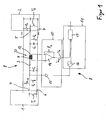
- the device according to the invention makes it possible to determine whether a transmission signal of the SIM card 1 or a transmission signal of the mobile telephone 2 is present on a communication line (I / O line) connecting the SIM card 1 to the mobile telephone 2.
- the communication line 3 is connected at each end to an input / output port (I / O port) 4 of the SIM card 1 and to an input / output port (I / O port) 5 of the cellular phone 2.
- a ground terminal 6 of the SIM card 1 is directly connected to a ground terminal 7 of the cellular phone 2.
- a pull-up resistor R P is arranged between the I / O terminal 5 of the mobile phone 2 and the supply voltage VCC. Based on the physical connection 7 arise due to the physical extent of the SIM card 1 and the mobile phone 2 on the communication line 3 parasitic capacitances in the FIG. 1 is symbolized by two capacitors C 1 , C 2 between the communication line 3 and the ground line 6, 7. The capacities can range between 10 pF and 30 pF. By the pull-up resistor R P , the capacitances C 1 , C 2 are recharged at rest.
- both capacitances C 1 , C 2 are discharged, the discharge current from the capacitor C 1 allowing a negative current I I / O to flow through a measuring circuit 8.
- the transistor T 1 of the SIM card 1 is turned on, the capacitor C 2 is discharged via the measuring circuit 8 with a positive current I I / O.
- the current generated by the pull-up resistor R P flows through the measuring circuit 8. The direction of the current flow peak through the measuring circuit 8 is decisive for the direction detection.
- the measuring circuit 8 essentially consists of a transformer 20 arranged between the I / O terminals 4 and 5 with a primary coil 9 and a secondary coil 12, with a signal conditioning unit 10 adjoining the secondary coil 12 of the transformer 12 and an evaluation unit downstream of the signal conditioning unit 10 11th
- the signal conditioning unit 10 has a measuring amplifier 14 and a resistor R F connected to the negative terminal of the measuring amplifier 14 and the output of the measuring amplifier 14. At the output of the signal conditioning unit 10 is a voltage U A , which forms an input of the evaluation.
- the evaluation unit 11 comprises on the one hand a measuring amplifier 15, at the input of which the voltage U 1 is applied to the communication line 3.
- a downstream of the measuring amplifier 15 edge detector 16 of the evaluation unit 11 detects a falling edge of the signal voltages U 1 , U 2 on the communication line 3 and thus sets the time for direction detection. Rising edges of the signal voltages U 1 , U 2 are not taken into account in the direction detection.
- the evaluation unit 11 has a comparator circuit 17, which may contain, for example, two comparators.
- the output voltage U A of the signal conditioning unit 10 is applied to the input of the comparator circuit 17. The exceeding of a threshold value or the undershooting of a further threshold value by the output signal U A can be detected by the comparator circuit 17.
- a direction signal U R which falls in response to the transmission direction from the high state to the low state or vice versa.
- the communication direction can be signaled by means of a display unit, not shown, or stored by means of a memory, not shown.
- the signal voltages U 1 , U 2 on the communication line 3 are in the high state. If the SIM card 1 sends a signal, the transistor T 1 is turned on, so that the signal voltage U 1 falls from the high state to the low state. As a result, the current I I / O increases abruptly, being composed by the discharge current of the capacitance C 2 and the current flowing through the pull-up resistor R P current component. In the transformer, a secondary current is induced in the secondary coil 12, which flows into the input of the measuring amplifier 14. Due to the wiring of the measuring amplifier, the induced current is compensated by the output voltage U A via R F.
- the output voltage U A of the measuring amplifier 14 has the same course as the current intensity I I / O , but has a level which is applied to the evaluation unit 11 is adjusted. As it turned out FIG. 2 results, a maximum value U Amax arises at the input of the comparator circuit 17 is applied. By comparison with a predetermined threshold, a direction voltage value U R at the output of the comparator circuit 17 decreases from the high state to the low state.
- the low state of the direction detection signal U R occurs after a time interval d T after the switching operation of the transistor T first
- the time interval d T defines the time interval between the switching instant of the transistor T 1 and the maximum value U Amax of the output voltage U A of the amplifier 14.
- FIG. 2 is a negative edge of the direction detection signal U R sending the SIM card 1, a positive edge of the signal U R sending of the mobile phone. 2
- the measuring circuit 8 is independent of the pull-up resistor R P. Decisive for the voltage or current peaks are the parasitic capacitances C 1 , C 2 .
- the measuring circuit 8 is particularly suitable for mobile phones with a relatively high-impedance pull-up resistor R P , which serves to minimize the power consumption of the mobile phone.
- the measuring circuit according to the invention it is only necessary for the communication line 3 to be passed through a transformer core. There are no additional components to attach to the communication line 3.
- the primary winding 9 of the transformer 20 consists of only one or a half turn.
- the communication line 3 is thus loaded only with a relatively small capacity. Furthermore, no significant voltage drops occur on the communication line 3 through the measuring circuit 8, which could lead to signal and communication disturbances.
Landscapes
- Engineering & Computer Science (AREA)
- Artificial Intelligence (AREA)
- Computer Vision & Pattern Recognition (AREA)
- Physics & Mathematics (AREA)
- General Physics & Mathematics (AREA)
- Theoretical Computer Science (AREA)
- Near-Field Transmission Systems (AREA)
- Radar Systems Or Details Thereof (AREA)
- Devices For Checking Fares Or Tickets At Control Points (AREA)
- Bidirectional Digital Transmission (AREA)
Description
- Die Erfindung betrifft eine Vorrichtung zur Erkennung der Datenübertragungsrichtung zwischen zwei Kommunikationseinheitennach dem Oberbegriff des Patentanspruchs 1.
- Aus der
DE 100 25 086 C1 ist eine Vorrichtung zur Erkennung der Datenübertragungsrichtung zwischen einem Datenträger und einer Datenträgerleseeinheit bekannt, die über eine Messschaltung verfügt. Die Messschaltung ist zwischen dem Eingangs-/Ausgangs-Anschluss (I/O-Anschluss) des Datenträgers und dem Eingangs-/Ausgangs-Anschluss (I/O-Anschluß) der Datenträgerleseeinheit, die mittels einer Verbindungsleitung (I/O-Leitung) miteinander verbunden sind, angeordnet. Die Messschaltung ist nach Art einer Brückenschaltung aufgebaut, wobei zwei Spannungsabfälle an unterschiedlichen Messpunkten gemessen und über Komparatorschaltungen miteinander verglichen werden. Durch Vergleich der gemessenen Spannungsabfälle bezogen auf einen vorgegebenen Schwellwert kann festgestellt werden, ob der Datenträger oder die Datenträgerleseeinheit als Kommunikationspartner sendet bzw. empfängt. Nachteilig an der bekannten Vorrichtung ist, dass der zur Auswertung benutzte Spannungsabfall eine Potenzialverschiebung verursacht. Weiterhin wird je nach Höhe des Widerstandswertes des Messwiderstandes das Kommunikationssignal zeitlich beeinflusst. Ferner ist diese Messschaltung empfindlich gegen Widerstandstoleranzen im Brückenzweig, da diese bereits im Ruhezustand der Schaltung zu einer Gleichspannungsaussteuerung der Komparatorschaltung führt. Ein weiterer wesentlicher Nachteil ist darin zu sehen, dass die Funktion der Messschaltung stark abhängig von dem Pull-Up-Widerstand zwischen dem I/O-Anschluss und dem Versorgungsanschluss (VCC) ist. Dieser Pull-UP-Widerstand bestimmt den Messstrom und beeinflusst somit im Wesentlichen den Spannungsabfall über den Messwiderstand. Ist der Pull-Up-Widerstand hochohmig, verringert sich der Spannungsabfall am Messwiderstand, so dass eine Richtungserkennung unter Umständen nicht möglich ist. - Aufgabe der vorliegenden Erfindung ist es daher, eine Vorrichtung zur Erkennung der Datenübertragungsrichtung zwischen einem Datenträger und einer Datenträgerleseeinheit derart weiterzubilden, dass die oben beschriebenen Nachteile beseitigt werden und eine sichere Richtungserkennung ermöglicht wird.
- Zur Lösung dieser Aufgabe weist die Erfindung die Merkmale des Patentanspruchs 1 auf.
- Der besondere Vorteil der Erfindung besteht darin, dass durch Erzeugung einer Stromspitze zusammen mit dem logischen Pegelwechsel auf der I/O-Leitung eindeutig und sicher die Datentransfer-Richtung bzw. Kommunikationsrichtung bestimmt werden kann. Die Polarität der Schaltspitze ist bei einem Pegelwechsel davon abhängig, welche der Kommunikationseinheiten den Wechsel hervorgerufen hat. Hierdurch ergibt sich ein unmittelbarer zeitlicher Bezug der Ausbildung der Schaltspitze zu dem Umschaltvorgang, dessen Lokalisierung durch die Auswerteschaltung erkannt wird. Schwankungen der Messparameter können daher nicht das Messergebnis verfälschen. Grundgedanke der Erfindung ist es, eine Messschaltung derart auszubilden, dass anhand eines eindeutig abgegrenzten Spitzenwertes die Datenübertragungsrichtung festgestellt werden kann. Durch vorzugsweise die Polarität des Spitzenwertes (positiv oder negativ) kann die Datenübertragungsrichtung in die eine oder andere Richtung erkannt werden.
- Nach einer Weiterbildung der Erfindung ist die Strom- und/oder Spannungsspitze als eine Schaltspitze ausgebildet, die sich unmittelbar nach dem Umschaltvorgang einstellt. Die Polarität der Schaltspitze ist davon abhängig, ob die Spannung an dem I/O-Anschluss des Datenträgers oder der Datenträgerleseeinheit von dem High-Zustand in den Low-Zustand gebracht worden ist. Hierdurch ergibt sich ein unmittelbarer zeitlicher Bezug der Ausbildung der Schaltspitze zu dem Umschaltvorgang, dessen Lokalisierung durch die Messschaltung erkannt wird.
- Weitere Vorteile der Erfindung ergeben sich aus den weiteren Unteransprüchen.
- Ein Ausführungsbeispiel der Erfindung ist nachfolgend anhand der Zeichnungen näher erläutert.
- Es zeigen:
- Figur 1
- einen Schaltplan einer erfindungsgemäßen Mess- schaltung und
- Figur 2
- ein Spannungs-/Strom-Zeitdiagramm.
- Eine erfindungsgemäße Vorrichtung zur Erkennung der Datenübertragungsrichtung zwischen zwei Kommunikationseinheiten kann zur Erkennung der Datenübertragungsrichtung zwischen einem Datenträger 1 und einer Datenträgerleseeinheit 2 eingesetzt werden. Sie ist vorzugsweise Bestandteil eines Messtools für Mobilfunktelefone bzw. SIM-Karten. Der Datenträger 1 ist als SIM-Karte und die Datenträgerleseeinheit 2 als Kartenleseeinheit eines Mobiltelefons ausgebildet. Die erfindungsgemäße Vorrichtung ermöglicht die Feststellung, ob auf einer die SIM-Karte 1 mit dem Mobiltelefon 2 verbindenden Kommunikationsleitung (I/O-Leitung) ein Sendesignal der SIM-Karte 1 oder ein Sendesignal des Mobiltelefon 2 anliegt. Die Kommunikationsleitung 3 ist jeweils endseitig an einem Eingangs-/Ausgangsanschluss (I/O-Anschluss) 4 der SIM-Karte 1 und an einem Eingangs-/Ausgangsanschluss (I/O-Anschluss) 5 des Mobiltelefons 2 angeschlossen ist. Ein Masseanschluss 6 der SIM-Karte 1 ist direkt mit einem Masseanschluss 7 des Mobiltelefons 2 verbunden.
- Zwischen dem I/O-Anschluss 5 des Mobiltelefons 2 und der Versorgungsspannung VCC ist ein Pull-Up-Widerstand RP angeordnet. Bezogen auf den Masseanschluss 7 entstehen auf Grund der physikalischen Ausdehnung der SIM-Karte 1 und des Mobiltelefons 2 auf der Kommunikationsleitung 3 parasitäre Kapazitäten, die in der
Figur 1 durch zwei Kondensatoren C1, C2 zwischen der Kommunikationsleitung 3 und der Masseleitung 6, 7 symbolisiert ist. Die Kapazitäten können in einem Bereich zwischen 10 pF und 30 pF liegen. Durch den Pull-Up-Widerstand RP werden die Kapazitäten C1,C2 im Ruhezustand wieder aufgeladen. Bei Schalten eines Transistors T2 des Mobiltelefons 2 werden beide Kapazitäten C1, C2 entladen, wobei der Entladestrom von der Kapazität C1 einen negativen Strom II/O durch eine Messschaltung 8 fließen lässt. Wird der Transistor T1 der SIM-Karte 1 eingeschaltet wird der Kondensator C2 über die Messschaltung 8 mit einem positiven Strom II/O entladen. Zusätzlich fließt noch der durch den Pull-Up-Widerstand RP generierte Strom durch die Messschaltung 8. Maßgeblich für die Richtungserkennung ist die Richtung der Stromflussspitze durch die Messschaltung 8. - Die Messschaltung 8 besteht im Wesentlichen aus einem zwischen den I/O-Anschlüssen 4 und 5 angeordneten Transformator 20 mit einer Primärspule 9 und einer Sekundärspule 12, mit einer sich an die Sekundärspule 12 des Transformators 12 anschließenden Signalaufbereitungseinheit 10 und einer der Signalaufbereitungseinheit 10 nachgeordneten Auswerteeinheit 11.
- Die Signalaufbereitungseinheit 10 weist einen Messverstärker 14 und einen an den negativen Anschluss des Messverstärkers 14 und dem Ausgang des Messverstärkers 14 angeschlossenen Widerstand RF auf. Am Ausgang der Signalaufbereitungseinheit 10 liegt eine Spannung UA an, die eine Eingangsgröße der Auswerteeinheit bildet.
- Die Auswerteeinheit 11 umfasst zum einen einen Messverstärker 15, an dessen Eingang die Spannung U1 an der Kommunikationsleitung 3 anliegt. Ein dem Messverstärker 15 nachgeschalteter Flankendetektor 16 der Auswerteeinheit 11 detektiert eine fallende Flanke der Signalspannungen U1, U2 an der Kommunikationsleitung 3 und legt damit den Zeitpunkt zur Richtungserkennung fest. Ansteigende Flanken der Signalspannungen U1, U2 werden nicht bei der Richtungserkennung berücksichtigt. Weiterhin weist die Auswerteeinheit 11 eine Komparatorschaltung 17 auf, die beispielsweise zwei Komparatoren enthalten kann. An dem Eingang der Komparatorschaltung 17 liegt ferner die Ausgangsspannung UA der Signalaufbereitungseinheit 10 an. Das Überschreiten eines Schwellenwertes bzw. das Unterschreiten eines weiteren Schwellenwertes durch das Ausgangssignal UA kann durch die Komparatorschaltung 17 detektiert werden. Am Ausgang der Auswerteeinheit 11 liegt ein Richtungssignal UR an, das in Abhängigkeit von der Übertragungsrichtung vom High-Zustand in den Low-Zustand oder umgekehrt fällt. Durch weitere logische Aufbereitung kann die Kommunikationsrichtung mittels einer nicht dargestellten Anzeigeeinheit signalisiert bzw. mittels eines nicht dargestellten Speichers abgespeichert werden.
- Im Folgenden wird die Funktionsweise der Messschaltung für zwei unterschiedliche Datenübertragungsrichtungen beschrieben. Im Ausgangszustand sind die Signalspannungen U1, U2 an der Kommunikationsleitung 3 im High-Zustand. Sendet die SIM-Karte 1 ein Signal, wird der Transistor T1 angeschaltet, so dass die Signalspannung U1 vom High-Zustand in den Low-Zustand fällt. Als Folge daraus steigt der Strom II/O schlagartig an, wobei er sich durch den Entladestrom der Kapazität C2 und den durch den Pull-Up-Widerstand RP durchflossenen Stromanteil zusammensetzt. In dem Transformator wird in der Sekundärspule 12 ein Sekundärstrom induziert, der in den Eingang des Messverstärkers 14 fließt. Aufgrund der Beschaltung des Messverstärkers wird der induzierte Strom durch die Ausgangsspannung UA über RF kompensiert. Die Ausgangsspannung UA des Messverstärkers 14 hat den gleichen Verlauf wie die Stromstärke II/O, weist jedoch ein Niveau auf, das an die Auswerteeinheit 11 angepasst ist. Wie sich aus
Figur 2 ergibt, entsteht ein Maximalwert UAmax der an dem Eingang der Komparatorschaltung 17 anliegt. Durch Vergleich mit einem vorgegebenen Schwellwert verringert sich ein Richtungsspannungswert UR am Ausgang der Komparatorschaltung 17 von dem High-Zustand in den Low-Zustand. Der Low-Zustand von dem Richtungserkennungssignal UR erfolgt nach einem Zeitintervall dT nach dem Schaltvorgang des Transistors T1. Das Zeitintervall dT legt den zeitlichen Abstand zwischen dem Schaltzeitpunkt des Transistors T1 und dem Maximalwert UAmax der Ausgangsspannung UA des Verstärkers 14 fest. - Erfolgt auf Grund der Ansteuerung des Transistors T2 ein Sendevorgang des Mobilfunkgerätes 2, fließt ein im Vergleich zum vorhergehenden Fall umgekehrter Strom II/O. Da kein Widerstand in Reihe liegt, erfolgt sowohl ein schlagartiger Anstieg als auch ein schlagartiger Abfall der Stromstärke II/O in negativer Richtung. Mittels des Transformators 20 erfolgt in gleicher Weise eine Übertragung des durch die Primärspule 9 fließenden Stroms an den Eingang des Messverstärkers 14. Das Ausgangssignal UA des Messverstärkers 14 weist den gleichen Verlauf auf wie die Stromstärke I0. Dadurch, dass ein Minimalwert UAmin mit entgegengesetzter Polarität im Vergleich zu dem anderen Sendevorgang sich einstellt, wird ein Richtungsspannungswert UR erzeugt, der von einem Low-Zustand in einen High-Zustand versetzt wird. Dies erfolgt in gleicher Weise mit einer Zeitverzögerung von dT nach dem Einschalten des Transistors T2.
- Wie besser aus
Figur 2 zu ersehen ist, bedeutet eine negative Flanke des Richtungserkennungssignals UR ein Senden der SIM-Karte 1, eine positive Flanke des Signals UR ein Senden des Mobiltelefons 2. - Vorteilhaft ist die erfindungsgemäße Messschaltung 8 unabhängig von dem Pull-Up-Widerstand RP. Maßgeblich für die Spannungs- bzw. Stromspitzen sind die parasitären Kapazitäten C1, C2. Die Messschaltung 8 eignet sich insbesondere auch für Mobiltelefone mit einem relativ hoch ohmigen Pull-Up-Widerstand RP, der zur Minimierung der Stromaufnahme des Mobiltelefons dient.
- Vorteilhaft ist nach der erfindungsgemäßen Messschaltung lediglich erforderlich, dass die Kommunikationsleitung 3 durch einen Transformatorkern hindurch geleitet werden muss. Es sind keine zusätzlichen Bauteile an der Kommunikationsleitung 3 anzubringen.
- Vorzugsweise besteht die Primärwicklung 9 des Transformators 20 nur aus einer bzw. einer halben Windung. Die Kommunikationsleitung 3 wird somit nur mit einer relativ kleinen Kapazität belastet. Weiterhin treten durch die Messschaltung 8 keine nennenswerten Spannungsabfälle an der Kommunikationsleitung 3 auf, die zu Signal- und Kommunikationsstörungen führen könnten.
Claims (6)
- vorrichtung zur Erkennung der Datenübertragungsrichtung zwischen zwei Kommunikationseinheiten,
wobei die Vorrichtung eine Messschaltung (8) enthält, die
einer die kommunikationseinheiten (1,2) verbindenden Kommunikationsleitung zugeordnet ist,
dadurch gekennzeichnet, dass
die Messschaltung (8) einen Transformator (20) umfasst, dessen Primärspule (9) zwischen den Eingangs-/Ausgangsanschlüssen (4, 5) der Kommunikationseinheiten (1, 2) angeordnet ist
und dass in der Messschaltung (8) eine Signalaufbereitungseinheit (10) mit einem Messverstärker (14) vorgesehen ist, an dessen Eingang die Sekundärspule (12) des Transformators (20) angeschlossen ist und der ein Stromsignal in ein Spannungssignal umwandelt,
wobei die Messschaltung (8) derart aufgebaut ist, dass beim Umschalten eines Eingangs-/Ausgangsanschlusses (4, 5) einer der Kommunikationseinheiten (1, 2) von einem logischen Zustand in einen anderen logischen Zustand eine Stromspitze (UAmax, UAmin) erzeugt wird,
und dass die Signalaufbereitungseinheit (10) einen mit der Kommunikationsleitung (3) verbundenen Messverstärker (15) und einen Flankendetektor (16) aufweist, der eine fallende Flanke der Signalspannung (U1, U2) der Kommunikationsleitung (3) detektiert,
so dass mittels einer Auswerteeinheit (11) in Abhängigkeit von dem Ausgangssignal des Flankendetektors (16) die Polarität der Stromspitze (UAmax, UAmin) ermittelt wird. - Vorrichtung nach Anspruch 1, dadurch gekennzeichnet, dass die Polarität der Stromspitze (UAmax, UAmin) abhängig von der Richtung der Datenübertragung ist.
- Vorrichtung nach Anspruch 1 oder 2, dadurch gekennzeichnet, dass die Stromspitze (UAmax, UAmin) als eine Schaltspitze ausgebildet ist, die unmittelbar nach dem Umschaltvorgang entsteht.
- Vorrichtung nach einem der Ansprüche 1 bis 3, dadurch gekennzeichnet, dass der Signalaufbereitungseinheit (10) eine Auswerteeinheit (11) nachgeordnet ist, in der ein Spannungsausgangswert (UA) der Signalaufbereitungseinheit (10) weiterverarbeitet wird, so dass in Abhängigkeit der Polarität des Spannungswertes (UR) die Richtung der Datenübertragung signalisierbar ist.
- Vorrichtung nach einem der Ansprüche 1 bis 4, dadurch gekennzeichnet, dass als Kommunikationseinheiten ein Datenträger (1) und eine Datenträgerleseeinheit (2) ausgebildet sind, die über die Kommunikationsleitung (3) und einer Masseleitung miteinander verbindbar sind.
- Vorrichtung nach Anspruch 5, dadurch gekennzeichnet, dass die Auswerteeinheit (11) mindestens einen Komparator aufweist, mittels dessen die Polarität der Ausgangsspannung (UA) des Messverstärkers (14) zum mittels des Flankendetektors (16) vorgegebenen Zeitpunkt ermittelbar ist.
Applications Claiming Priority (2)
| Application Number | Priority Date | Filing Date | Title |
|---|---|---|---|
| DE102005050457A DE102005050457A1 (de) | 2005-10-19 | 2005-10-19 | Vorrichtung zur Erkennung der Datenübertragungsrichtung zwischen Kommunikationspartnern |
| PCT/DE2006/001607 WO2007045196A1 (de) | 2005-10-19 | 2006-09-12 | Vorrichtung zur erkennung der datenübertragungsrichtung zwischen kommunikationspartnern |
Publications (2)
| Publication Number | Publication Date |
|---|---|
| EP1938241A1 EP1938241A1 (de) | 2008-07-02 |
| EP1938241B1 true EP1938241B1 (de) | 2009-11-25 |
Family
ID=37547517
Family Applications (1)
| Application Number | Title | Priority Date | Filing Date |
|---|---|---|---|
| EP06791376A Not-in-force EP1938241B1 (de) | 2005-10-19 | 2006-09-12 | Vorrichtung zur erkennung der datenübertragungsrichtung zwischen kommunikationspartnern |
Country Status (4)
| Country | Link |
|---|---|
| EP (1) | EP1938241B1 (de) |
| AT (1) | ATE450014T1 (de) |
| DE (2) | DE102005050457A1 (de) |
| WO (1) | WO2007045196A1 (de) |
Families Citing this family (2)
| Publication number | Priority date | Publication date | Assignee | Title |
|---|---|---|---|---|
| ATE518325T1 (de) | 2008-06-13 | 2011-08-15 | Comprion Gmbh | Verfahren und vorrichtung zur erkennung eines digitalen signals |
| CN106908674B (zh) * | 2017-02-17 | 2020-02-07 | 国网上海市电力公司 | 一种基于多状态量预测的变压器状态评估方法 |
Family Cites Families (2)
| Publication number | Priority date | Publication date | Assignee | Title |
|---|---|---|---|---|
| DE19725917A1 (de) * | 1997-06-19 | 1999-01-07 | Telefunken Microelectron | Sende- und Empfangsvorrichtung, insbesondere für periphere Module eines Steuersystems mit einer die Module steuernden Zentraleinheit |
| DE10025086C1 (de) * | 2000-05-20 | 2001-12-20 | Orga Kartensysteme Gmbh | Verfahren zur Überwachung der Datenübertragung |
-
2005
- 2005-10-19 DE DE102005050457A patent/DE102005050457A1/de not_active Withdrawn
-
2006
- 2006-09-12 WO PCT/DE2006/001607 patent/WO2007045196A1/de not_active Ceased
- 2006-09-12 EP EP06791376A patent/EP1938241B1/de not_active Not-in-force
- 2006-09-12 DE DE502006005472T patent/DE502006005472D1/de active Active
- 2006-09-12 AT AT06791376T patent/ATE450014T1/de active
Also Published As
| Publication number | Publication date |
|---|---|
| EP1938241A1 (de) | 2008-07-02 |
| WO2007045196A1 (de) | 2007-04-26 |
| DE102005050457A1 (de) | 2007-04-26 |
| DE502006005472D1 (de) | 2010-01-07 |
| ATE450014T1 (de) | 2009-12-15 |
Similar Documents
| Publication | Publication Date | Title |
|---|---|---|
| DE112017002593B4 (de) | Ansteuerregelungsgerät für ein schaltbauelement | |
| DE69802065T2 (de) | Hybrider regler | |
| DE10229460B3 (de) | Spannungsfolger und ASK-Demodulator mit einem Spannungsfolger | |
| DE69505274T2 (de) | Fensterkomparator mit echter hysterese | |
| DE10233220B3 (de) | Komparator mit Hysterese | |
| DE102004017863B4 (de) | Schaltung und Verfahren zum Ermitteln eines Referenzpegels für eine solche Schaltung | |
| DE10393465T5 (de) | Stromintegrierender Leseverstärker für Speichermodule bei der RFID | |
| DE102020131060A1 (de) | Intelligenter elektronischer schalter | |
| DE102007024064B4 (de) | Strombegrenzungs-System, Schaltung und Verfahren zur Strombegrenzung | |
| DE10229459C1 (de) | Transponder | |
| DE102011015498B4 (de) | Eingangsschaltung für eine Eingangsbaugruppe und Verfahren zum Betreiben einer Eingangsschaltung | |
| DE19651548C2 (de) | CMOS-Ausgangsschaltung mit einer Ladevorspannungsschaltung | |
| EP1314095A1 (de) | Erkennung eines geräte-anschlusszustands beim usb | |
| WO1999042952A1 (de) | Datenträger sowohl für den kontaktlosen als auch den kontaktbehafteten betrieb | |
| DE102007053089A1 (de) | Elektrisches und elektronisches System | |
| DE102019203338A1 (de) | Ringing-Entstörschaltung | |
| EP0763746A2 (de) | Schaltungsanordnung zum Erkennen des Leerlaufs einer Last | |
| EP1026569B1 (de) | Spannungsregler | |
| DE102010042156A1 (de) | Übertragungsvorrichtung für eine differentielle Kommunikation | |
| EP1769422B1 (de) | Modulator und modulationsverfahren für eine einrichtung zur drahtlosen datenübertragung | |
| EP1938241A1 (de) | Vorrichtung zur erkennung der datenübertragungsrichtung zwischen kommunikationspartnern | |
| DE60122646T2 (de) | Signalkompensierungsschaltung und Demodulatorschaltung | |
| DE102004060211A1 (de) | Integrierte Schaltung mit einem Unterspannungsdetektor | |
| WO2005027549A1 (de) | Verlängerung der sim-karten-schnittstelle in gsm-geräten | |
| DE19604041C1 (de) | Schaltungsanordnung zur Erkennung eines durch eine Last fließenden Laststroms |
Legal Events
| Date | Code | Title | Description |
|---|---|---|---|
| PUAI | Public reference made under article 153(3) epc to a published international application that has entered the european phase |
Free format text: ORIGINAL CODE: 0009012 |
|
| 17P | Request for examination filed |
Effective date: 20070705 |
|
| AK | Designated contracting states |
Kind code of ref document: A1 Designated state(s): AT BE BG CH CY CZ DE DK EE ES FI FR GB GR HU IE IS IT LI LT LU LV MC NL PL PT RO SE SI SK TR |
|
| 17Q | First examination report despatched |
Effective date: 20080819 |
|
| GRAP | Despatch of communication of intention to grant a patent |
Free format text: ORIGINAL CODE: EPIDOSNIGR1 |
|
| DAX | Request for extension of the european patent (deleted) | ||
| GRAS | Grant fee paid |
Free format text: ORIGINAL CODE: EPIDOSNIGR3 |
|
| GRAA | (expected) grant |
Free format text: ORIGINAL CODE: 0009210 |
|
| AK | Designated contracting states |
Kind code of ref document: B1 Designated state(s): AT BE BG CH CY CZ DE DK EE ES FI FR GB GR HU IE IS IT LI LT LU LV MC NL PL PT RO SE SI SK TR |
|
| REG | Reference to a national code |
Ref country code: GB Ref legal event code: FG4D Free format text: NOT ENGLISH |
|
| REG | Reference to a national code |
Ref country code: CH Ref legal event code: EP |
|
| REG | Reference to a national code |
Ref country code: IE Ref legal event code: FG4D |
|
| REF | Corresponds to: |
Ref document number: 502006005472 Country of ref document: DE Date of ref document: 20100107 Kind code of ref document: P |
|
| REG | Reference to a national code |
Ref country code: NL Ref legal event code: T3 |
|
| LTIE | Lt: invalidation of european patent or patent extension |
Effective date: 20091125 |
|
| PG25 | Lapsed in a contracting state [announced via postgrant information from national office to epo] |
Ref country code: IS Free format text: LAPSE BECAUSE OF FAILURE TO SUBMIT A TRANSLATION OF THE DESCRIPTION OR TO PAY THE FEE WITHIN THE PRESCRIBED TIME-LIMIT Effective date: 20100325 Ref country code: PT Free format text: LAPSE BECAUSE OF FAILURE TO SUBMIT A TRANSLATION OF THE DESCRIPTION OR TO PAY THE FEE WITHIN THE PRESCRIBED TIME-LIMIT Effective date: 20100325 Ref country code: FI Free format text: LAPSE BECAUSE OF FAILURE TO SUBMIT A TRANSLATION OF THE DESCRIPTION OR TO PAY THE FEE WITHIN THE PRESCRIBED TIME-LIMIT Effective date: 20091125 Ref country code: LT Free format text: LAPSE BECAUSE OF FAILURE TO SUBMIT A TRANSLATION OF THE DESCRIPTION OR TO PAY THE FEE WITHIN THE PRESCRIBED TIME-LIMIT Effective date: 20091125 Ref country code: SE Free format text: LAPSE BECAUSE OF FAILURE TO SUBMIT A TRANSLATION OF THE DESCRIPTION OR TO PAY THE FEE WITHIN THE PRESCRIBED TIME-LIMIT Effective date: 20091125 |
|
| PG25 | Lapsed in a contracting state [announced via postgrant information from national office to epo] |
Ref country code: SI Free format text: LAPSE BECAUSE OF FAILURE TO SUBMIT A TRANSLATION OF THE DESCRIPTION OR TO PAY THE FEE WITHIN THE PRESCRIBED TIME-LIMIT Effective date: 20091125 Ref country code: LV Free format text: LAPSE BECAUSE OF FAILURE TO SUBMIT A TRANSLATION OF THE DESCRIPTION OR TO PAY THE FEE WITHIN THE PRESCRIBED TIME-LIMIT Effective date: 20091125 Ref country code: PL Free format text: LAPSE BECAUSE OF FAILURE TO SUBMIT A TRANSLATION OF THE DESCRIPTION OR TO PAY THE FEE WITHIN THE PRESCRIBED TIME-LIMIT Effective date: 20091125 Ref country code: CY Free format text: LAPSE BECAUSE OF FAILURE TO SUBMIT A TRANSLATION OF THE DESCRIPTION OR TO PAY THE FEE WITHIN THE PRESCRIBED TIME-LIMIT Effective date: 20091125 |
|
| REG | Reference to a national code |
Ref country code: IE Ref legal event code: FD4D |
|
| PG25 | Lapsed in a contracting state [announced via postgrant information from national office to epo] |
Ref country code: IE Free format text: LAPSE BECAUSE OF FAILURE TO SUBMIT A TRANSLATION OF THE DESCRIPTION OR TO PAY THE FEE WITHIN THE PRESCRIBED TIME-LIMIT Effective date: 20091125 Ref country code: RO Free format text: LAPSE BECAUSE OF FAILURE TO SUBMIT A TRANSLATION OF THE DESCRIPTION OR TO PAY THE FEE WITHIN THE PRESCRIBED TIME-LIMIT Effective date: 20091125 Ref country code: EE Free format text: LAPSE BECAUSE OF FAILURE TO SUBMIT A TRANSLATION OF THE DESCRIPTION OR TO PAY THE FEE WITHIN THE PRESCRIBED TIME-LIMIT Effective date: 20091125 Ref country code: BG Free format text: LAPSE BECAUSE OF FAILURE TO SUBMIT A TRANSLATION OF THE DESCRIPTION OR TO PAY THE FEE WITHIN THE PRESCRIBED TIME-LIMIT Effective date: 20100225 Ref country code: DK Free format text: LAPSE BECAUSE OF FAILURE TO SUBMIT A TRANSLATION OF THE DESCRIPTION OR TO PAY THE FEE WITHIN THE PRESCRIBED TIME-LIMIT Effective date: 20091125 Ref country code: ES Free format text: LAPSE BECAUSE OF FAILURE TO SUBMIT A TRANSLATION OF THE DESCRIPTION OR TO PAY THE FEE WITHIN THE PRESCRIBED TIME-LIMIT Effective date: 20100308 |
|
| PG25 | Lapsed in a contracting state [announced via postgrant information from national office to epo] |
Ref country code: SK Free format text: LAPSE BECAUSE OF FAILURE TO SUBMIT A TRANSLATION OF THE DESCRIPTION OR TO PAY THE FEE WITHIN THE PRESCRIBED TIME-LIMIT Effective date: 20091125 Ref country code: CZ Free format text: LAPSE BECAUSE OF FAILURE TO SUBMIT A TRANSLATION OF THE DESCRIPTION OR TO PAY THE FEE WITHIN THE PRESCRIBED TIME-LIMIT Effective date: 20091125 |
|
| RAP2 | Party data changed (patent owner data changed or rights of a patent transferred) |
Owner name: COMPRION GMBH |
|
| PLBE | No opposition filed within time limit |
Free format text: ORIGINAL CODE: 0009261 |
|
| STAA | Information on the status of an ep patent application or granted ep patent |
Free format text: STATUS: NO OPPOSITION FILED WITHIN TIME LIMIT |
|
| PG25 | Lapsed in a contracting state [announced via postgrant information from national office to epo] |
Ref country code: GR Free format text: LAPSE BECAUSE OF FAILURE TO SUBMIT A TRANSLATION OF THE DESCRIPTION OR TO PAY THE FEE WITHIN THE PRESCRIBED TIME-LIMIT Effective date: 20100226 |
|
| 26N | No opposition filed |
Effective date: 20100826 |
|
| PG25 | Lapsed in a contracting state [announced via postgrant information from national office to epo] |
Ref country code: IT Free format text: LAPSE BECAUSE OF FAILURE TO SUBMIT A TRANSLATION OF THE DESCRIPTION OR TO PAY THE FEE WITHIN THE PRESCRIBED TIME-LIMIT Effective date: 20091125 |
|
| PG25 | Lapsed in a contracting state [announced via postgrant information from national office to epo] |
Ref country code: MC Free format text: LAPSE BECAUSE OF NON-PAYMENT OF DUE FEES Effective date: 20100930 |
|
| REG | Reference to a national code |
Ref country code: CH Ref legal event code: PL |
|
| PG25 | Lapsed in a contracting state [announced via postgrant information from national office to epo] |
Ref country code: LI Free format text: LAPSE BECAUSE OF NON-PAYMENT OF DUE FEES Effective date: 20100930 Ref country code: CH Free format text: LAPSE BECAUSE OF NON-PAYMENT OF DUE FEES Effective date: 20100930 |
|
| PG25 | Lapsed in a contracting state [announced via postgrant information from national office to epo] |
Ref country code: HU Free format text: LAPSE BECAUSE OF FAILURE TO SUBMIT A TRANSLATION OF THE DESCRIPTION OR TO PAY THE FEE WITHIN THE PRESCRIBED TIME-LIMIT Effective date: 20100526 Ref country code: LU Free format text: LAPSE BECAUSE OF NON-PAYMENT OF DUE FEES Effective date: 20100912 |
|
| PG25 | Lapsed in a contracting state [announced via postgrant information from national office to epo] |
Ref country code: TR Free format text: LAPSE BECAUSE OF FAILURE TO SUBMIT A TRANSLATION OF THE DESCRIPTION OR TO PAY THE FEE WITHIN THE PRESCRIBED TIME-LIMIT Effective date: 20091125 |
|
| REG | Reference to a national code |
Ref country code: AT Ref legal event code: MM01 Ref document number: 450014 Country of ref document: AT Kind code of ref document: T Effective date: 20110912 |
|
| PG25 | Lapsed in a contracting state [announced via postgrant information from national office to epo] |
Ref country code: AT Free format text: LAPSE BECAUSE OF NON-PAYMENT OF DUE FEES Effective date: 20110912 |
|
| PGFP | Annual fee paid to national office [announced via postgrant information from national office to epo] |
Ref country code: GB Payment date: 20140923 Year of fee payment: 9 |
|
| PGFP | Annual fee paid to national office [announced via postgrant information from national office to epo] |
Ref country code: NL Payment date: 20140922 Year of fee payment: 9 |
|
| PGFP | Annual fee paid to national office [announced via postgrant information from national office to epo] |
Ref country code: BE Payment date: 20140917 Year of fee payment: 9 |
|
| REG | Reference to a national code |
Ref country code: FR Ref legal event code: PLFP Year of fee payment: 10 |
|
| PGFP | Annual fee paid to national office [announced via postgrant information from national office to epo] |
Ref country code: DE Payment date: 20150929 Year of fee payment: 10 |
|
| PGFP | Annual fee paid to national office [announced via postgrant information from national office to epo] |
Ref country code: FR Payment date: 20150923 Year of fee payment: 10 |
|
| GBPC | Gb: european patent ceased through non-payment of renewal fee |
Effective date: 20150912 |
|
| REG | Reference to a national code |
Ref country code: NL Ref legal event code: MM Effective date: 20151001 |
|
| PG25 | Lapsed in a contracting state [announced via postgrant information from national office to epo] |
Ref country code: GB Free format text: LAPSE BECAUSE OF NON-PAYMENT OF DUE FEES Effective date: 20150912 |
|
| PG25 | Lapsed in a contracting state [announced via postgrant information from national office to epo] |
Ref country code: NL Free format text: LAPSE BECAUSE OF NON-PAYMENT OF DUE FEES Effective date: 20151001 |
|
| REG | Reference to a national code |
Ref country code: DE Ref legal event code: R119 Ref document number: 502006005472 Country of ref document: DE |
|
| REG | Reference to a national code |
Ref country code: FR Ref legal event code: ST Effective date: 20170531 |
|
| PG25 | Lapsed in a contracting state [announced via postgrant information from national office to epo] |
Ref country code: DE Free format text: LAPSE BECAUSE OF NON-PAYMENT OF DUE FEES Effective date: 20170401 Ref country code: FR Free format text: LAPSE BECAUSE OF NON-PAYMENT OF DUE FEES Effective date: 20160930 Ref country code: BE Free format text: LAPSE BECAUSE OF NON-PAYMENT OF DUE FEES Effective date: 20150930 |