EP1937041A2 - Printed circuit board, light emitting apparatus having the same and manufacturing method thereof - Google Patents
Printed circuit board, light emitting apparatus having the same and manufacturing method thereof Download PDFInfo
- Publication number
- EP1937041A2 EP1937041A2 EP07123640A EP07123640A EP1937041A2 EP 1937041 A2 EP1937041 A2 EP 1937041A2 EP 07123640 A EP07123640 A EP 07123640A EP 07123640 A EP07123640 A EP 07123640A EP 1937041 A2 EP1937041 A2 EP 1937041A2
- Authority
- EP
- European Patent Office
- Prior art keywords
- light emitting
- metal layer
- emitting device
- circuit board
- printed circuit
- Prior art date
- Legal status (The legal status is an assumption and is not a legal conclusion. Google has not performed a legal analysis and makes no representation as to the accuracy of the status listed.)
- Granted
Links
Images

Classifications
-
- H—ELECTRICITY
- H05—ELECTRIC TECHNIQUES NOT OTHERWISE PROVIDED FOR
- H05K—PRINTED CIRCUITS; CASINGS OR CONSTRUCTIONAL DETAILS OF ELECTRIC APPARATUS; MANUFACTURE OF ASSEMBLAGES OF ELECTRICAL COMPONENTS
- H05K1/00—Printed circuits
- H05K1/02—Details
- H05K1/0201—Thermal arrangements, e.g. for cooling, heating or preventing overheating
- H05K1/0203—Cooling of mounted components
- H05K1/021—Components thermally connected to metal substrates or heat-sinks by insert mounting
-
- H—ELECTRICITY
- H10—SEMICONDUCTOR DEVICES; ELECTRIC SOLID-STATE DEVICES NOT OTHERWISE PROVIDED FOR
- H10H—INORGANIC LIGHT-EMITTING SEMICONDUCTOR DEVICES HAVING POTENTIAL BARRIERS
- H10H20/00—Individual inorganic light-emitting semiconductor devices having potential barriers, e.g. light-emitting diodes [LED]
- H10H20/80—Constructional details
- H10H20/85—Packages
- H10H20/8506—Containers
-
- H—ELECTRICITY
- H10—SEMICONDUCTOR DEVICES; ELECTRIC SOLID-STATE DEVICES NOT OTHERWISE PROVIDED FOR
- H10H—INORGANIC LIGHT-EMITTING SEMICONDUCTOR DEVICES HAVING POTENTIAL BARRIERS
- H10H20/00—Individual inorganic light-emitting semiconductor devices having potential barriers, e.g. light-emitting diodes [LED]
- H10H20/80—Constructional details
- H10H20/85—Packages
- H10H20/858—Means for heat extraction or cooling
-
- H—ELECTRICITY
- H10—SEMICONDUCTOR DEVICES; ELECTRIC SOLID-STATE DEVICES NOT OTHERWISE PROVIDED FOR
- H10H—INORGANIC LIGHT-EMITTING SEMICONDUCTOR DEVICES HAVING POTENTIAL BARRIERS
- H10H29/00—Integrated devices, or assemblies of multiple devices, comprising at least one light-emitting semiconductor element covered by group H10H20/00
- H10H29/80—Constructional details
- H10H29/85—Packages
- H10H29/8508—Package substrates, e.g. submounts
-
- H—ELECTRICITY
- H05—ELECTRIC TECHNIQUES NOT OTHERWISE PROVIDED FOR
- H05K—PRINTED CIRCUITS; CASINGS OR CONSTRUCTIONAL DETAILS OF ELECTRIC APPARATUS; MANUFACTURE OF ASSEMBLAGES OF ELECTRICAL COMPONENTS
- H05K1/00—Printed circuits
- H05K1/02—Details
- H05K1/03—Use of materials for the substrate
- H05K1/05—Insulated conductive substrates, e.g. insulated metal substrate
- H05K1/056—Insulated conductive substrates, e.g. insulated metal substrate the metal substrate being covered by an organic insulating layer
-
- H—ELECTRICITY
- H05—ELECTRIC TECHNIQUES NOT OTHERWISE PROVIDED FOR
- H05K—PRINTED CIRCUITS; CASINGS OR CONSTRUCTIONAL DETAILS OF ELECTRIC APPARATUS; MANUFACTURE OF ASSEMBLAGES OF ELECTRICAL COMPONENTS
- H05K1/00—Printed circuits
- H05K1/18—Printed circuits structurally associated with non-printed electric components
- H05K1/182—Printed circuits structurally associated with non-printed electric components associated with components mounted in printed circuit boards [PCB], e.g. insert-mounted components [IMC]
-
- H—ELECTRICITY
- H05—ELECTRIC TECHNIQUES NOT OTHERWISE PROVIDED FOR
- H05K—PRINTED CIRCUITS; CASINGS OR CONSTRUCTIONAL DETAILS OF ELECTRIC APPARATUS; MANUFACTURE OF ASSEMBLAGES OF ELECTRICAL COMPONENTS
- H05K2201/00—Indexing scheme relating to printed circuits covered by H05K1/00
- H05K2201/09—Shape and layout
- H05K2201/09209—Shape and layout details of conductors
- H05K2201/09654—Shape and layout details of conductors covering at least two types of conductors provided for in H05K2201/09218 - H05K2201/095
- H05K2201/09745—Recess in conductor, e.g. in pad or in metallic substrate
-
- H—ELECTRICITY
- H05—ELECTRIC TECHNIQUES NOT OTHERWISE PROVIDED FOR
- H05K—PRINTED CIRCUITS; CASINGS OR CONSTRUCTIONAL DETAILS OF ELECTRIC APPARATUS; MANUFACTURE OF ASSEMBLAGES OF ELECTRICAL COMPONENTS
- H05K2201/00—Indexing scheme relating to printed circuits covered by H05K1/00
- H05K2201/10—Details of components or other objects attached to or integrated in a printed circuit board
- H05K2201/10007—Types of components
- H05K2201/10106—Light emitting diode [LED]
-
- H—ELECTRICITY
- H05—ELECTRIC TECHNIQUES NOT OTHERWISE PROVIDED FOR
- H05K—PRINTED CIRCUITS; CASINGS OR CONSTRUCTIONAL DETAILS OF ELECTRIC APPARATUS; MANUFACTURE OF ASSEMBLAGES OF ELECTRICAL COMPONENTS
- H05K2203/00—Indexing scheme relating to apparatus or processes for manufacturing printed circuits covered by H05K3/00
- H05K2203/02—Details related to mechanical or acoustic processing, e.g. drilling, punching, cutting, using ultrasound
- H05K2203/0207—Partly drilling through substrate until a controlled depth, e.g. with end-point detection
-
- H—ELECTRICITY
- H05—ELECTRIC TECHNIQUES NOT OTHERWISE PROVIDED FOR
- H05K—PRINTED CIRCUITS; CASINGS OR CONSTRUCTIONAL DETAILS OF ELECTRIC APPARATUS; MANUFACTURE OF ASSEMBLAGES OF ELECTRICAL COMPONENTS
- H05K3/00—Apparatus or processes for manufacturing printed circuits
- H05K3/0011—Working of insulating substrates or insulating layers
- H05K3/0044—Mechanical working of the substrate, e.g. drilling or punching
- H05K3/0047—Drilling of holes
-
- H—ELECTRICITY
- H05—ELECTRIC TECHNIQUES NOT OTHERWISE PROVIDED FOR
- H05K—PRINTED CIRCUITS; CASINGS OR CONSTRUCTIONAL DETAILS OF ELECTRIC APPARATUS; MANUFACTURE OF ASSEMBLAGES OF ELECTRICAL COMPONENTS
- H05K3/00—Apparatus or processes for manufacturing printed circuits
- H05K3/30—Assembling printed circuits with electric components, e.g. with resistors
- H05K3/32—Assembling printed circuits with electric components, e.g. with resistors electrically connecting electric components or wires to printed circuits
- H05K3/34—Assembling printed circuits with electric components, e.g. with resistors electrically connecting electric components or wires to printed circuits by soldering
- H05K3/341—Surface mounted components
- H05K3/3421—Leaded components
-
- Y—GENERAL TAGGING OF NEW TECHNOLOGICAL DEVELOPMENTS; GENERAL TAGGING OF CROSS-SECTIONAL TECHNOLOGIES SPANNING OVER SEVERAL SECTIONS OF THE IPC; TECHNICAL SUBJECTS COVERED BY FORMER USPC CROSS-REFERENCE ART COLLECTIONS [XRACs] AND DIGESTS
- Y10—TECHNICAL SUBJECTS COVERED BY FORMER USPC
- Y10T—TECHNICAL SUBJECTS COVERED BY FORMER US CLASSIFICATION
- Y10T29/00—Metal working
- Y10T29/49—Method of mechanical manufacture
- Y10T29/49002—Electrical device making
- Y10T29/49117—Conductor or circuit manufacturing
- Y10T29/49124—On flat or curved insulated base, e.g., printed circuit, etc.
- Y10T29/4913—Assembling to base an electrical component, e.g., capacitor, etc.
Definitions
- the present invention relates to a printed circuit board, a light emitting apparatus having the same and a manufacturing method thereof, and more particularly to a printed circuit board capable of improving reliability, a light emitting apparatus having the same and a manufacturing method thereof.
- a light emitting diode (hereinafter, referred to as "LED”) is a device which realizes light emission based on a field effect by depositing a compound semiconductor thin film on a substrate. Recently, the LED is widely used as a display unit of various electronic appliances for lighting, communication and the like.
- the LED is operated by injecting electrons and holes and emitting energy generated in combination of the electrons and holes in the form of light. In this case, some energy is emitted in the form of heat.
- the generated heat can be relieved by a proper heat sink in manufacturing a package.
- the present invention is directed to a printed circuit board, a light emitting apparatus having the same and a manufacturing method thereof that substantially obviate one or more problems due to limitations and disadvantages of the related art.
- An object of the present invention is to provide a printed circuit board capable of efficiently emitting heat generated from a light emitting device, a light emitting apparatus having the printed circuit board and a manufacturing method thereof.
- a printed circuit board mounted with a light emitting device package comprises: a first metal layer; an insulating layer disposed on the first metal layer; a second metal layer disposed on the insulating layer; and a mounting groove for mounting the light emitting device package, which has a depth reaching at least an upper surface of the first metal layer.
- a light emitting apparatus comprises: a first metal layer; an insulating layer disposed on the first metal layer; a second metal layer disposed on the insulating layer; a mounting groove for mounting a light emitting device package, which has a depth reaching at least an upper surface of the first metal layer; and a light emitting device package mounted on the mounting groove.
- a manufacturing method of a light emitting apparatus comprises: preparing a printed circuit board in which a first metal layer, an insulating layer and a second metal layer are sequentially stacked; forming a mounting groove on the printed circuit board to have a depth reaching at least an upper surface of the first metal layer; and mounting a light emitting device package including a heat sink on the mounting groove formed on the printed circuit board.
- FIG. 1 illustrates a cross-sectional view showing a first embodiment of the present invention
- FIG. 2 illustrates a cross-sectional view showing a printed circuit board according to a second embodiment of the present invention
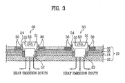
- FIG. 3 illustrates a cross-sectional view showing a light emitting apparatus according to the second embodiment of the present invention.
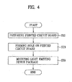
- FIG. 4 illustrates a flowchart showing a manufacturing method of the light emitting apparatus according to the second embodiment of the present invention.
- first and second are used to describe various elements, components, areas, layers and/or zones, it is to be understood that the elements, components, areas, layers and/or zones are not limited by those terms.
- FIG. 1 A first embodiment of the present invention will be described with reference to FIG. 1 .
- a light emitting apparatus including a metal core printed circuit board may be formed by mounting a light emitting device package 6 on a printed circuit board 5.
- the printed circuit board 5 of the light emitting apparatus may employ one of circuit boards having various shapes.
- a light emitting module using a high output light emitting device package may employ a metal core printed circuit board (MCPCB) in which a first metal layer 1, an insulating layer 2, a second metal layer 3 and a solder resist layer 4 are sequentially stacked.
- MCPCB metal core printed circuit board
- an aluminum layer is used as the first metal layer 1 and a copper layer is used as the second metal layer 3 on the aluminum layer to form a circuit.
- the insulating layer 2 formed of an insulating material such as epoxy may be positioned between the first metal layer 1 and the second metal layer 3.
- the first metal layer 1 and the second metal layer 3 may be formed of various metals such as iron and silver as well as the above-mentioned aluminum and copper.
- solder resist layer 4 is disposed on the second metal layer 3. In this case, the solder resist layer 4 is removed only at a portion to be coated with solder for combining the second metal layer 3 with parts.
- the light emitting device package 6 mounted with a light emitting device chip is attached to the second metal layer 3 of the metal core printed circuit board by a solder 7 through the portion without the solder resist layer 4.
- heat generated from the light emitting device package 6 may be emitted into the air through the solder 7, the second metal layer 3, the insulating layer 2 and the first metal layer 1.
- the emitted heat is in proportion to a heat radiation area and in inverse proportion to a distance, heat is transferred along a vertical moving route with respect to the light emitting device package.
- the thermal conductivity becomes lower.
- the heat is in proportion to a heat radiation area and in inverse proportion to a moving distance.
- the second metal layer 3 formed of copper since a portion which is directly contacted to the light emitting device package 6 is the second metal layer 3 formed of copper, it may be difficult to smoothly emit heat to the first metal layer 1.
- a printed circuit board 10 is formed by sequentially stacking a first metal layer 12, an insulating layer 14, a second metal layer 16 and a solder resist layer 18.
- a mounting groove 40 for mounting a light emitting device package is formed on the printed circuit board 10 to have a depth reaching at least an upper surface of the first metal layer 12.
- the mounting groove 40 may be formed to be deeper than the upper surface of the first metal layer 12 by a specified depth.
- the mounting groove 40 may be formed to have substantially the same size as that of a light emitting device package to be mounted such that the light emitting device package can be closely contacted to the mounting groove 40.
- the mounting groove 40 may have different shapes and depths according to the type and size of the light emitting device package to be mounted.
- an aluminum layer is used as the first metal layer 12 and the second metal layer 16 formed of copper is disposed on the aluminum layer to form a circuit.
- the insulating layer 14 formed of an insulating material such as epoxy is positioned between the first metal layer 12 and the second metal layer 16.
- the first metal layer 12 and the second metal layer 16 may be formed of various metals such as iron and silver as well as the above-mentioned aluminum and copper.
- the first metal layer 12 may have a thickness larger than that of the second metal layer 16 forming a circuit, which may vary according to a height of the light emitting device package to be mounted.
- a light emitting device package 50 is mounted on the mounting groove 40 of the printed circuit board 10.
- the light emitting device package 50 includes a package body 51 with a mounting portion 55, a heat sink 52 attached to the lower side of the package body 51 and a light emitting device 53 mounted on the mounting portion 55.
- the mounting portion 55 may be formed in the shape of an inwardly recessed groove.
- the heat sink 52 is connected to the lower side of the package body 51 to form a heat transfer route.
- a lead 54 electrically connected to the light emitting device 53 is at the side of the package body 51.
- the lead 54 is electrically connected to the second metal layer 16 through a solder 30 disposed at a portion from which the solder resist layer 18 has been removed.
- solder 30 is also coated between the heat sink 52 of the light emitting device package 50 and the first metal layer 12 such that heat generated from the light emitting device 53 is efficiently conducted to the first metal layer 12.
- solder 30 is positioned between the heat sink 52 and the first metal layer 12, thereby firmly fixing the light emitting device package 50 on the printed circuit board 10. Further, a contact area between the heat sink 52 and the first metal layer 12 may be enlarged through the solder 30.
- the heat sink 52 has a height capable of reaching the first metal layer 12 when the light emitting device package 50 is installed on the printed circuit board 10. Accordingly, the heat sink 52 may have a shape protruded downward from the light emitting device package 50.
- the lead 54 when the light emitting device package 50 is mounted on the mounting groove formed on the printed circuit board 10, the lead 54 may be positioned properly for soldering in a state where the heat sink 52 of the light emitting device package 50 is in contact with the first metal layer 12.
- the solder 30 for mounting the light emitting device package 50 may be formed by coating cream solder and hardening the solder through a proper process such as a process of applying heat.
- a heat emission route of a light emitting apparatus including the printed circuit board 10 and the light emitting device package 50 is described below.
- the light emitting device package 50 is closely contacted to the first metal layer 12 through the heat sink 52.
- the heat generated from the light emitting device package 50 may be emitted through the closely contacted first metal layer 12.
- the heat generated from the light emitting device package 50 is directly transferred to the first metal layer 12 of the printed circuit board 10. Accordingly, the moving distance of heat is largely reduced and it is effective for heat radiation.
- L refers to a thickness of a surface perpendicular to heat flow and k refers to thermal conductivity. Further, A refers to an area of the surface perpendicular to heat flow.
- the heat radiation effect is more excellent as the thermal resistance is lower.
- the thickness L should be small and the area A should be large. Accordingly, the moving distance of heat, that is, the number of layers through which heat moves, should be reduced to enhance the heat radiation effect.
- the thermal resistance is expressed by the following equation.
- R th R 2 ⁇ nd metal + R insulating layer + R 1 ⁇ st metal
- thermal resistance according to the second embodiment is expressed by the following equation.
- the thermal resistance is calculated exclusive of the resistance due to the second metal layer 16 and the resistance due to the insulating layer 14, it is possible to significantly improve heat transfer compared to the first embodiment or a general MCPCB.
- the printed circuit board 10 in which the first metal layer 12, the insulating layer 14, the second metal layer 16 and the solder resist layer 18 are sequentially stacked (S10). That is because it is advantageous to employ the metal core printed circuit board 10 including the above-described metal layers 12 and 16 in the light emitting device module using a high output light emitting device.
- the solder resist layer 18 is a coating layer which coats the second metal layer 16.
- a different layer such as paint, a PSR layer and a polymer layer may be provided instead of the solder resist layer 18 to coat the second metal layer 16 forming circuit lines.
- the mounting groove 40 for the light emitting device package is formed on the printed circuit board 10 to have a depth reaching at least the upper surface of the first metal layer 12 (S20).
- the mounting groove 40 may be formed through a drilling process by a computer numerical control (CNC) method. Further, the mounting groove 40 may be formed to have different sizes by changing a drill size according to the size of the light emitting device package 50.
- CNC computer numerical control
- a hole may be formed on the printed circuit board 10 by a computer numerical control method using X-Y coordinates based on the information of the mounting groove 40 requested for designing the printed circuit board 10.
- the depth of the mounting groove 40 is determined based on the information of the thickness of the heat sink 52 of the light emitting device package 50.
- the depth of the mounting groove 40 is determined such that the heat sink 52 is closely contacted to the first metal layer 12.
- the light emitting device package 50 is mounted on the printed circuit board 10 with the mounting groove 40 (S30).
- the mounting process is performed by coating cream solder on the heat sink 52 of the light emitting device package 50 and a portion of the second metal layer 16 corresponding to the lead 54 and hardening the solder through a hardening process, for example, heat hardening. Consequently, the heat sink 52 is coupled to the first metal layer 12 and the lead 54 is coupled to the second metal layer 16.
Landscapes
- Engineering & Computer Science (AREA)
- Microelectronics & Electronic Packaging (AREA)
- Led Device Packages (AREA)
- Cooling Or The Like Of Semiconductors Or Solid State Devices (AREA)
Abstract
Description
- This application claims the benefit of
Korean Patent Application No. 10-2006-0131i40, filed on December 21, 2006 - The present invention relates to a printed circuit board, a light emitting apparatus having the same and a manufacturing method thereof, and more particularly to a printed circuit board capable of improving reliability, a light emitting apparatus having the same and a manufacturing method thereof.
- A light emitting diode (hereinafter, referred to as "LED") is a device which realizes light emission based on a field effect by depositing a compound semiconductor thin film on a substrate. Recently, the LED is widely used as a display unit of various electronic appliances for lighting, communication and the like.
- Among various application fields of LED, a lighting field has been actively researched to replace a back light unit (BLU) used in a thin LCD TV and a fluorescence lamp. Further, the structure, material and package of LED have been vigorously researched to apply the LED to the application fields.
- The LED is operated by injecting electrons and holes and emitting energy generated in combination of the electrons and holes in the form of light. In this case, some energy is emitted in the form of heat. The generated heat can be relieved by a proper heat sink in manufacturing a package.
- However, as a high output LED having an LED chip size of 1 mm x 1 mm or more is developed, it is possible to achieve the LED brightness of 10 CD or more. By arranging several high output chips, it is possible to use various LED modules, for example, an electric signboard, a back light unit and a lighting module.
- In such an application product, since a large number of LEDs are provided, the temperature of heat emitted from the LEDs is very high. Further, since the LED brightness is in proportion to the LED heat, it is necessary to solve a heat problem in an LED module such as a printed circuit board mounted with the LED.
- Accordingly, the present invention is directed to a printed circuit board, a light emitting apparatus having the same and a manufacturing method thereof that substantially obviate one or more problems due to limitations and disadvantages of the related art.
- An object of the present invention is to provide a printed circuit board capable of efficiently emitting heat generated from a light emitting device, a light emitting apparatus having the printed circuit board and a manufacturing method thereof.
- Additional advantages, objects, and features of the invention will be set forth in part in the description which follows and in part will become apparent to those having ordinary skill in the art upon examination of the following or may be learned from practice of the invention. The objectives and other advantages of the invention may be realized and attained by the structure particularly pointed out in the written description and claims hereof as well as the appended drawings.
- To achieve these objects and other advantages and in accordance with the purpose of the invention, as embodied and broadly described herein, a printed circuit board mounted with a light emitting device package comprises: a first metal layer; an insulating layer disposed on the first metal layer; a second metal layer disposed on the insulating layer; and a mounting groove for mounting the light emitting device package, which has a depth reaching at least an upper surface of the first metal layer.
- In another aspect of the present invention, a light emitting apparatus comprises: a first metal layer; an insulating layer disposed on the first metal layer; a second metal layer disposed on the insulating layer; a mounting groove for mounting a light emitting device package, which has a depth reaching at least an upper surface of the first metal layer; and a light emitting device package mounted on the mounting groove.
- In yet another aspect of the present invention, a manufacturing method of a light emitting apparatus comprises: preparing a printed circuit board in which a first metal layer, an insulating layer and a second metal layer are sequentially stacked; forming a mounting groove on the printed circuit board to have a depth reaching at least an upper surface of the first metal layer; and mounting a light emitting device package including a heat sink on the mounting groove formed on the printed circuit board.
- It is to be understood that both the foregoing general description and the following detailed description of the present invention are exemplary and explanatory and are intended to provide further explanation of the invention as claimed.
- The accompanying drawings, which are included to provide a further understanding of the invention and are incorporated in and constitute a part of this application, illustrate embodiment(s) of the invention and together with the description serve to explain the principle of the invention. In the drawings:
-
FIG. 1 illustrates a cross-sectional view showing a first embodiment of the present invention; -
FIG. 2 illustrates a cross-sectional view showing a printed circuit board according to a second embodiment of the present invention; -
FIG. 3 illustrates a cross-sectional view showing a light emitting apparatus according to the second embodiment of the present invention; and -
FIG. 4 illustrates a flowchart showing a manufacturing method of the light emitting apparatus according to the second embodiment of the present invention. - Reference will now be made in detail to the preferred embodiments of the present invention, examples of which are illustrated in the accompanying drawings. Wherever possible, the same reference numbers will be used throughout the drawings to refer to the same or like parts.
- Hereinafter, embodiments of the present invention will be described in detail with reference to the accompanying drawings.
- Since there can be a variety of permutations and embodiments of the present invention, certain embodiments will be illustrated and described with reference to the accompanying drawings. This, however, is by no means to restrict the present invention to certain embodiments, and shall be construed as including all permutations, equivalents and substitutes covered by the spirit and scope of the present invention.
- It is to be understood that when an element such as a layer, an area or a substrate is described to exist "on" the other element, it may directly exist on the other element or an intermediate element may exist between them. It is to be understood that when a part of an element such as surface is expressed as "inner", it is further away from the outside of the device than other parts of the element.
- Further, relative terms such as "beneath" or "overlies" will be used to describe the relation between one layer or area and the other layer or the relation between one layer of an area and the area with respect to a substrate or a reference layer as shown in the drawings.
- It is to be understood that these terms are intended to cover another aspects of devices in addition to aspects depicted in the drawings. Finally, the term "directly" means that no element is interposed between devices. The term "and/or" includes one or more combinations of related lists, and all combinations.
- Although the terms such as "first" and "second" are used to describe various elements, components, areas, layers and/or zones, it is to be understood that the elements, components, areas, layers and/or zones are not limited by those terms.
- <first embodiment>
- A first embodiment of the present invention will be described with reference to
FIG. 1 . - As shown in
FIG. 1 , a light emitting apparatus including a metal core printed circuit board may be formed by mounting a lightemitting device package 6 on a printed circuit board 5. - The printed circuit board 5 of the light emitting apparatus may employ one of circuit boards having various shapes. However, a light emitting module using a high output light emitting device package may employ a metal core printed circuit board (MCPCB) in which a first metal layer 1, an insulating layer 2, a second metal layer 3 and a solder resist layer 4 are sequentially stacked.
- As an example of the structure of the metal core printed circuit board, an aluminum layer is used as the first metal layer 1 and a copper layer is used as the second metal layer 3 on the aluminum layer to form a circuit. In order to electrically insulate the first metal layer 1 from the second metal layer 3, the insulating layer 2 formed of an insulating material such as epoxy may be positioned between the first metal layer 1 and the second metal layer 3.
- The first metal layer 1 and the second metal layer 3 may be formed of various metals such as iron and silver as well as the above-mentioned aluminum and copper.
- Further, the solder resist layer 4 is disposed on the second metal layer 3. In this case, the solder resist layer 4 is removed only at a portion to be coated with solder for combining the second metal layer 3 with parts.
- The light
emitting device package 6 mounted with a light emitting device chip is attached to the second metal layer 3 of the metal core printed circuit board by a solder 7 through the portion without the solder resist layer 4. - In the structure of the light emitting apparatus, heat generated from the light
emitting device package 6 may be emitted into the air through the solder 7, the second metal layer 3, the insulating layer 2 and the first metal layer 1. In this case, since the emitted heat is in proportion to a heat radiation area and in inverse proportion to a distance, heat is transferred along a vertical moving route with respect to the light emitting device package. - Generally, as there are a larger number of the boundaries between materials, the thermal conductivity becomes lower. The heat is in proportion to a heat radiation area and in inverse proportion to a moving distance. In the above-described structure of the light emitting apparatus, since there are many routes of heat transfer, the moving distance becomes long.
- Further, since a portion which is directly contacted to the light
emitting device package 6 is the second metal layer 3 formed of copper, it may be difficult to smoothly emit heat to the first metal layer 1. - <second embodiment>
- Hereinafter, a second embodiment of the present invention will be described with reference to
FIGs. 2 to 4 . - As shown in
FIG. 2 , a printedcircuit board 10 according to the second embodiment is formed by sequentially stacking afirst metal layer 12, aninsulating layer 14, asecond metal layer 16 and asolder resist layer 18. In this case, a mountinggroove 40 for mounting a light emitting device package is formed on the printedcircuit board 10 to have a depth reaching at least an upper surface of thefirst metal layer 12. - As shown in
FIG. 2 , the mountinggroove 40 may be formed to be deeper than the upper surface of thefirst metal layer 12 by a specified depth. The mountinggroove 40 may be formed to have substantially the same size as that of a light emitting device package to be mounted such that the light emitting device package can be closely contacted to the mountinggroove 40. - That is, the mounting
groove 40 may have different shapes and depths according to the type and size of the light emitting device package to be mounted. - In this case, an aluminum layer is used as the
first metal layer 12 and thesecond metal layer 16 formed of copper is disposed on the aluminum layer to form a circuit. The insulatinglayer 14 formed of an insulating material such as epoxy is positioned between thefirst metal layer 12 and thesecond metal layer 16. - The
first metal layer 12 and thesecond metal layer 16 may be formed of various metals such as iron and silver as well as the above-mentioned aluminum and copper. - The
first metal layer 12 may have a thickness larger than that of thesecond metal layer 16 forming a circuit, which may vary according to a height of the light emitting device package to be mounted. - As shown in
FIG. 3 , a light emittingdevice package 50 is mounted on the mountinggroove 40 of the printedcircuit board 10. - The light emitting
device package 50 includes apackage body 51 with a mountingportion 55, aheat sink 52 attached to the lower side of thepackage body 51 and alight emitting device 53 mounted on the mountingportion 55. The mountingportion 55 may be formed in the shape of an inwardly recessed groove. - As shown in the drawings, the
heat sink 52 is connected to the lower side of thepackage body 51 to form a heat transfer route. A lead 54 electrically connected to thelight emitting device 53 is at the side of thepackage body 51. - The
lead 54 is electrically connected to thesecond metal layer 16 through asolder 30 disposed at a portion from which the solder resistlayer 18 has been removed. - Further, the
solder 30 is also coated between theheat sink 52 of the light emittingdevice package 50 and thefirst metal layer 12 such that heat generated from thelight emitting device 53 is efficiently conducted to thefirst metal layer 12. - That is, the
solder 30 is positioned between theheat sink 52 and thefirst metal layer 12, thereby firmly fixing the light emittingdevice package 50 on the printedcircuit board 10. Further, a contact area between theheat sink 52 and thefirst metal layer 12 may be enlarged through thesolder 30. - As shown in
FIG. 3 , it is advantageous that theheat sink 52 has a height capable of reaching thefirst metal layer 12 when the light emittingdevice package 50 is installed on the printedcircuit board 10. Accordingly, theheat sink 52 may have a shape protruded downward from the light emittingdevice package 50. - That is, with regard to the thickness of each layer of the printed
circuit board 10 and the height of the light emittingdevice package 50, when the light emittingdevice package 50 is mounted on the mounting groove formed on the printedcircuit board 10, thelead 54 may be positioned properly for soldering in a state where theheat sink 52 of the light emittingdevice package 50 is in contact with thefirst metal layer 12. - In this case, the
solder 30 for mounting the light emittingdevice package 50 may be formed by coating cream solder and hardening the solder through a proper process such as a process of applying heat. - A heat emission route of a light emitting apparatus including the printed
circuit board 10 and the light emittingdevice package 50 is described below. - As described above, the light emitting
device package 50 is closely contacted to thefirst metal layer 12 through theheat sink 52. The heat generated from the light emittingdevice package 50 may be emitted through the closely contactedfirst metal layer 12. - In other words, the heat generated from the light emitting
device package 50 is directly transferred to thefirst metal layer 12 of the printedcircuit board 10. Accordingly, the moving distance of heat is largely reduced and it is effective for heat radiation. - Compared to the first embodiment, although heat is transferred through the solder 7, the second metal layer 3, the insulating layer 2 and the first metal layer 1 in the light emitting apparatus of the first embodiment, heat is transferred and emitted to the outside through only the
first metal layer 12 in the light emitting apparatus including the printedcircuit board 10 according to the second embodiment. Thus, the number of layers through which heat moves is reduced and the moving distance of heat is also reduced, thereby having an excellent heat radiation effect. - In order to promote the understanding of heat transfer in the present invention, a formula for thermal resistance Rth is expressed in Eq. 1.
-

- In Eq. 1, L refers to a thickness of a surface perpendicular to heat flow and k refers to thermal conductivity. Further, A refers to an area of the surface perpendicular to heat flow.
- That is, it means that the heat radiation effect is more excellent as the thermal resistance is lower. In order to decrease the thermal resistance, the thickness L should be small and the area A should be large. Accordingly, the moving distance of heat, that is, the number of layers through which heat moves, should be reduced to enhance the heat radiation effect.
- Thus, in the first embodiment or a general MCPCB, the thermal resistance is expressed by the following equation.
-

- However, the thermal resistance according to the second embodiment is expressed by the following equation.
-

- That is, in the second embodiment, since the thermal resistance is calculated exclusive of the resistance due to the
second metal layer 16 and the resistance due to the insulatinglayer 14, it is possible to significantly improve heat transfer compared to the first embodiment or a general MCPCB. - Hereinafter, a method of manufacturing the light emitting apparatus according to the second embodiment will be described with reference to
FIGs. 2 to 4 . - First, there is prepared the printed
circuit board 10 in which thefirst metal layer 12, the insulatinglayer 14, thesecond metal layer 16 and the solder resistlayer 18 are sequentially stacked (S10). That is because it is advantageous to employ the metal core printedcircuit board 10 including the above-describedmetal layers - The solder resist
layer 18 is a coating layer which coats thesecond metal layer 16. A different layer such as paint, a PSR layer and a polymer layer may be provided instead of the solder resistlayer 18 to coat thesecond metal layer 16 forming circuit lines. - Then, the mounting
groove 40 for the light emitting device package is formed on the printedcircuit board 10 to have a depth reaching at least the upper surface of the first metal layer 12 (S20). - It is preferable to form the mounting
groove 40 through a drilling process by a computer numerical control (CNC) method. Further, the mountinggroove 40 may be formed to have different sizes by changing a drill size according to the size of the light emittingdevice package 50. - In the drilling process, a hole may be formed on the printed
circuit board 10 by a computer numerical control method using X-Y coordinates based on the information of the mountinggroove 40 requested for designing the printedcircuit board 10. - Further, the depth of the mounting
groove 40 is determined based on the information of the thickness of theheat sink 52 of the light emittingdevice package 50. - In other words, in order that heat generated from the light emitting
device package 50 is transferred directly to thefirst metal layer 12, the depth of the mountinggroove 40 is determined such that theheat sink 52 is closely contacted to thefirst metal layer 12. - Finally, the light emitting
device package 50 is mounted on the printedcircuit board 10 with the mounting groove 40 (S30). The mounting process is performed by coating cream solder on theheat sink 52 of the light emittingdevice package 50 and a portion of thesecond metal layer 16 corresponding to thelead 54 and hardening the solder through a hardening process, for example, heat hardening. Consequently, theheat sink 52 is coupled to thefirst metal layer 12 and thelead 54 is coupled to thesecond metal layer 16. - It will be apparent to those skilled in the art that various modifications and variations can be made in the present invention without departing from the spirit or scope of the inventions. Thus, it is intended that the present invention covers the modifications and variations of this invention provided they come within the scope of the appended claims and their equivalents.
Claims (20)
- A printed circuit board mounted with a light emitting device package, comprising:a first metal layer;an insulating layer disposed on the first metal layer;a second metal layer disposed on the insulating layer; anda mounting groove for mounting the light emitting device package, which has a depth reaching at least an upper surface of the first metal layer.
- The printed circuit board according to claim 1, wherein the first metal layer is an aluminum layer and the second metal layer is a copper layer.
- The printed circuit board according to claim 1, further comprising a solder resist layer disposed on the second metal layer.
- The printed circuit board according to claim 1, wherein the mounting groove has substantially the same width as that of the light emitting device package.
- The printed circuit board according to claim 1, wherein the first metal layer has a thickness larger than that of the second metal layer.
- A light emitting apparatus, comprising:a first metal layer;an insulating layer disposed on the first metal layer;a second metal layer disposed on the insulating layer;a mounting groove for mounting a light emitting device package, which has a depth reaching at least an upper surface of the first metal layer; anda light emitting device package mounted on the mounting groove.
- The light emitting apparatus according to claim 6, wherein the light emitting device package includes:a package body with a light emitting device mounting portion;a light emitting device mounted on the mounting portion;a lead which is installed on the package body and is electrically connected to the light emitting device; anda heat sink in contact with a lower side of the package body.
- The light emitting apparatus according to claim 7, wherein the lead is connected to the second metal layer by a solder positioned on the second metal layer.
- The light emitting apparatus according to claim 6, further comprising a coating layer disposed on the second metal layer.
- The light emitting apparatus according to claim 9, wherein the coating layer is a solder resist.
- The light emitting apparatus according to claim 7, wherein the heat sink is in contact with the first metal layer.
- The light emitting apparatus according to claim 11, wherein the heat sink is in contact with the first metal layer through a solder.
- The light emitting apparatus according to claim 6, wherein the first metal layer is an aluminum layer and the second metal layer is a copper layer.
- A manufacturing method of a light emitting apparatus, comprising:preparing a printed circuit board in which a first metal layer, an insulating layer and a second metal layer are sequentially stacked;forming a mounting groove on the printed circuit board to have a depth reaching at least an upper surface of the first metal layer; andmounting a light emitting device package including a heat sink on the mounting groove formed on the printed circuit board.
- The manufacturing method according to claim 14, wherein the step of forming a mounting groove is performed by a drilling process.
- The manufacturing method according to claim 14, wherein the step of forming a mounting groove is controlled by a computer numerical control (CNC) method.
- The manufacturing method according to claim 14, wherein the light emitting device package is mounted on the mounting groove by a solder.
- The manufacturing method according to claim 17, wherein the solder connects the light emitting device package to the second metal layer or connects the heat sink of the light emitting device package to the first metal layer.
- The manufacturing method according to claim 17, wherein a solder resist is further disposed on the second metal layer where the solder is not disposed.
- The manufacturing method according to claim 14, wherein a depth of the mounting groove is determined based on information of a thickness of the heat sink of the light emitting device package.
Applications Claiming Priority (1)
| Application Number | Priority Date | Filing Date | Title |
|---|---|---|---|
| KR1020060131740A KR20080057881A (en) | 2006-12-21 | 2006-12-21 | Printed circuit board, light emitting device comprising same and manufacturing method thereof |
Publications (3)
| Publication Number | Publication Date |
|---|---|
| EP1937041A2 true EP1937041A2 (en) | 2008-06-25 |
| EP1937041A3 EP1937041A3 (en) | 2009-07-15 |
| EP1937041B1 EP1937041B1 (en) | 2011-05-25 |
Family
ID=39283862
Family Applications (1)
| Application Number | Title | Priority Date | Filing Date |
|---|---|---|---|
| EP07123640A Active EP1937041B1 (en) | 2006-12-21 | 2007-12-19 | Printed circuit board, light emitting apparatus having the same and manufacturing method thereof |
Country Status (4)
| Country | Link |
|---|---|
| US (1) | US20080149373A1 (en) |
| EP (1) | EP1937041B1 (en) |
| JP (1) | JP2008160128A (en) |
| KR (1) | KR20080057881A (en) |
Cited By (5)
| Publication number | Priority date | Publication date | Assignee | Title |
|---|---|---|---|---|
| WO2010077760A1 (en) * | 2008-12-17 | 2010-07-08 | Alcoa Inc. | Led lighting laminate with integrated cooling |
| EP2209144A1 (en) * | 2008-12-29 | 2010-07-21 | LG Innotek Co., Ltd. | Light emitting device package |
| EP2219235A3 (en) * | 2009-02-17 | 2010-11-17 | LG Innotek Co., Ltd. | Light emitting device package |
| EP2325547A1 (en) * | 2009-10-29 | 2011-05-25 | Chia-Cheng Chang | 360-degree angle LED illumination device |
| CN104654247A (en) * | 2013-11-25 | 2015-05-27 | 海洋王(东莞)照明科技有限公司 | Heat dissipation structure of LED lamp, manufacturing method thereof, and LED lamp |
Families Citing this family (19)
| Publication number | Priority date | Publication date | Assignee | Title |
|---|---|---|---|---|
| KR101498682B1 (en) * | 2008-08-20 | 2015-03-04 | 삼성전자주식회사 | Light emitting diode module |
| KR100982473B1 (en) * | 2008-08-25 | 2010-09-15 | (주)미백창호 | Aluminum panel system with LED lighting |
| KR100910746B1 (en) * | 2009-03-30 | 2009-08-05 | (주)보다테크놀로지 | LED radiator |
| KR101352276B1 (en) * | 2009-07-24 | 2014-01-16 | 엘지디스플레이 주식회사 | Apparatus for radiating heat of light emitting diode and liquid crystal display using the same |
| KR20110086648A (en) * | 2010-01-15 | 2011-07-29 | 엘지이노텍 주식회사 | Light emitting module, backlight unit and display device |
| KR101064146B1 (en) * | 2010-02-26 | 2011-09-16 | 박재순 | Surface mount light emitting unit array, repair method thereof and light emitting unit for repair |
| KR101098533B1 (en) * | 2010-03-31 | 2011-12-26 | (주)포인트엔지니어링 | Optical Element Module and fabricating method thereof |
| US20110304270A1 (en) * | 2010-06-10 | 2011-12-15 | Eco Lumens, Llc | Light emitting diode (led) lighting systems and methods |
| KR101690509B1 (en) * | 2010-07-05 | 2016-12-28 | 엘지이노텍 주식회사 | Light emitting module and light emitting system using the light emitting module |
| KR20120012150A (en) * | 2010-07-30 | 2012-02-09 | 엘지디스플레이 주식회사 | LCD Display |
| KR101730140B1 (en) | 2010-08-02 | 2017-04-25 | 엘지디스플레이 주식회사 | Liquid crystal display device |
| KR101779205B1 (en) * | 2010-10-06 | 2017-09-26 | 엘지이노텍 주식회사 | The radiant heat circuit board and the heat generating device package having the same |
| TWI400824B (en) * | 2010-12-08 | 2013-07-01 | 友達光電股份有限公司 | Light source module and backlight module |
| KR20120118686A (en) * | 2011-04-19 | 2012-10-29 | 엘지이노텍 주식회사 | Light emitting device module |
| KR101835529B1 (en) | 2011-08-09 | 2018-03-08 | 삼성디스플레이 주식회사 | Display apparutus and light source package for the same |
| CN103148409B (en) * | 2013-01-31 | 2015-01-21 | 深圳市华星光电技术有限公司 | Back light source and method for manufacturing back light source |
| DE102016107249B4 (en) * | 2016-04-19 | 2022-12-15 | Infineon Technologies Austria Ag | Printed circuit board with a recess for an electrical component, system with the printed circuit board and method for manufacturing the printed circuit board |
| CN111341750B (en) * | 2018-12-19 | 2024-03-01 | 奥特斯奥地利科技与系统技术有限公司 | Component carrier including conductive base structure and method of manufacturing |
| US20240074031A1 (en) * | 2022-08-29 | 2024-02-29 | Creeled, Inc. | Textured metal core printed circuit boards for improved thermal dissipation |
Citations (1)
| Publication number | Priority date | Publication date | Assignee | Title |
|---|---|---|---|---|
| KR20060131740A (en) | 2003-10-10 | 2006-12-20 | 꼼미사리아 아 레네르지 아토미끄 | Recording and reading method for magnetic tunnel junction and magnetic tunnel junction |
Family Cites Families (27)
| Publication number | Priority date | Publication date | Assignee | Title |
|---|---|---|---|---|
| US4835598A (en) * | 1985-06-13 | 1989-05-30 | Matsushita Electric Works, Ltd. | Wiring board |
| US6392159B1 (en) * | 1999-07-27 | 2002-05-21 | International Business Machines Corporation | Embedded structure for engineering change and repair of circuit boards |
| US6874910B2 (en) * | 2001-04-12 | 2005-04-05 | Matsushita Electric Works, Ltd. | Light source device using LED, and method of producing same |
| US20040012958A1 (en) * | 2001-04-23 | 2004-01-22 | Takuma Hashimoto | Light emitting device comprising led chip |
| US7055987B2 (en) * | 2001-09-13 | 2006-06-06 | Lucea Ag | LED-luminous panel and carrier plate |
| US6531328B1 (en) * | 2001-10-11 | 2003-03-11 | Solidlite Corporation | Packaging of light-emitting diode |
| US7429757B2 (en) * | 2002-06-19 | 2008-09-30 | Sanken Electric Co., Ltd. | Semiconductor light emitting device capable of increasing its brightness |
| WO2004038759A2 (en) * | 2002-08-23 | 2004-05-06 | Dahm Jonathan S | Method and apparatus for using light emitting diodes |
| EP1590994B1 (en) * | 2003-02-07 | 2016-05-18 | Panasonic Intellectual Property Management Co., Ltd. | Metal base wiring board for retaining light emitting elements, light emitting source, lighting apparatus, and display apparatus |
| WO2004105142A1 (en) * | 2003-05-26 | 2004-12-02 | Matsushita Electric Works, Ltd. | Light-emitting device |
| DE10351934B4 (en) * | 2003-11-07 | 2017-07-13 | Tridonic Jennersdorf Gmbh | Light-emitting diode arrangement with heat dissipating board |
| DE102004009284A1 (en) * | 2004-02-26 | 2005-09-15 | Osram Opto Semiconductors Gmbh | Light-emitting diode arrangement for a high-performance light-emitting diode and method for producing a light-emitting diode arrangement |
| TWI257184B (en) * | 2004-03-24 | 2006-06-21 | Toshiba Lighting & Technology | Lighting apparatus |
| JP4632690B2 (en) * | 2004-05-11 | 2011-02-16 | スタンレー電気株式会社 | Semiconductor light emitting device and manufacturing method thereof |
| KR100623024B1 (en) * | 2004-06-10 | 2006-09-19 | 엘지전자 주식회사 | High Power LED Package |
| US7476913B2 (en) * | 2004-08-10 | 2009-01-13 | Renesas Technology Corp. | Light emitting device having a mirror portion |
| US7443023B2 (en) * | 2004-09-03 | 2008-10-28 | Entorian Technologies, Lp | High capacity thin module system |
| US7324352B2 (en) * | 2004-09-03 | 2008-01-29 | Staktek Group L.P. | High capacity thin module system and method |
| KR100646093B1 (en) * | 2004-12-17 | 2006-11-15 | 엘지이노텍 주식회사 | Light emitting device package |
| KR101115800B1 (en) * | 2004-12-27 | 2012-03-08 | 엘지디스플레이 주식회사 | Light-emitting device package, method for fabricating the same and backlight unit |
| KR101197046B1 (en) * | 2005-01-26 | 2012-11-06 | 삼성디스플레이 주식회사 | Two dimensional light source of using light emitting diode and liquid crystal display panel of using the two dimensional light source |
| KR100945621B1 (en) * | 2005-03-07 | 2010-03-04 | 로무 가부시키가이샤 | Optical communication module and its manufacturing method |
| US7411225B2 (en) * | 2005-03-21 | 2008-08-12 | Lg Electronics Inc. | Light source apparatus |
| EP1897146A2 (en) * | 2005-06-27 | 2008-03-12 | Lamina Lighting, Inc. | Light emitting diode package and method for making same |
| KR100592508B1 (en) * | 2005-07-15 | 2006-06-26 | 한국광기술원 | High Power LED Package with Beacon Shaped Substrate |
| WO2007072967A1 (en) * | 2005-12-19 | 2007-06-28 | Showa Denko K.K. | Flip-chip type semiconductor light-emitting device, method for manufacturing flip-chip type semiconductor light-emitting device, printed circuit board for flip-chip type semiconductor light-emitting device, mounting structure for flip-chip type semiconductor light-emitting device-and light-emitting diode lamp |
| KR100854328B1 (en) * | 2006-07-07 | 2008-08-28 | 엘지전자 주식회사 | Light emitting device package and its manufacturing method |
-
2006
- 2006-12-21 KR KR1020060131740A patent/KR20080057881A/en not_active Ceased
-
2007
- 2007-12-12 US US12/000,460 patent/US20080149373A1/en not_active Abandoned
- 2007-12-19 EP EP07123640A patent/EP1937041B1/en active Active
- 2007-12-21 JP JP2007329972A patent/JP2008160128A/en not_active Withdrawn
Patent Citations (1)
| Publication number | Priority date | Publication date | Assignee | Title |
|---|---|---|---|---|
| KR20060131740A (en) | 2003-10-10 | 2006-12-20 | 꼼미사리아 아 레네르지 아토미끄 | Recording and reading method for magnetic tunnel junction and magnetic tunnel junction |
Cited By (8)
| Publication number | Priority date | Publication date | Assignee | Title |
|---|---|---|---|---|
| WO2010077760A1 (en) * | 2008-12-17 | 2010-07-08 | Alcoa Inc. | Led lighting laminate with integrated cooling |
| EP2209144A1 (en) * | 2008-12-29 | 2010-07-21 | LG Innotek Co., Ltd. | Light emitting device package |
| US8227824B2 (en) | 2008-12-29 | 2012-07-24 | Lg Innotek Co., Ltd. | Light emitting device package |
| EP2219235A3 (en) * | 2009-02-17 | 2010-11-17 | LG Innotek Co., Ltd. | Light emitting device package |
| US8410513B2 (en) | 2009-02-17 | 2013-04-02 | Lg Innotek Co., Ltd. | Light emitting device package |
| US8829538B2 (en) | 2009-02-17 | 2014-09-09 | Lg Innotek Co., Ltd. | Light emitting device package |
| EP2325547A1 (en) * | 2009-10-29 | 2011-05-25 | Chia-Cheng Chang | 360-degree angle LED illumination device |
| CN104654247A (en) * | 2013-11-25 | 2015-05-27 | 海洋王(东莞)照明科技有限公司 | Heat dissipation structure of LED lamp, manufacturing method thereof, and LED lamp |
Also Published As
| Publication number | Publication date |
|---|---|
| JP2008160128A (en) | 2008-07-10 |
| EP1937041B1 (en) | 2011-05-25 |
| US20080149373A1 (en) | 2008-06-26 |
| EP1937041A3 (en) | 2009-07-15 |
| KR20080057881A (en) | 2008-06-25 |
Similar Documents
| Publication | Publication Date | Title |
|---|---|---|
| EP1937041B1 (en) | Printed circuit board, light emitting apparatus having the same and manufacturing method thereof | |
| US7745844B2 (en) | Light-emitting diode package and manufacturing method thereof | |
| US7335522B2 (en) | Package structure for light emitting diode and method thereof | |
| KR100764388B1 (en) | Anodized Metal Substrate Module | |
| US7192163B2 (en) | Light-emitting unit with enhanced thermal dissipation and method for fabricating the same | |
| US20100032705A1 (en) | Light emitting diode package and method of manufacturing the same | |
| US8895871B2 (en) | Circuit board having a plurality of circuit board layers arranged one over the other having bare die mounting for use as a gearbox controller | |
| JP5640281B2 (en) | Package substrate and manufacturing method thereof | |
| CN101997078A (en) | Substrate for light emitting device package and light emitting device package comprising the same | |
| US20090085180A1 (en) | Packaging carrier with high heat dissipation and method for manufacturing the same | |
| US7923271B1 (en) | Method of assembling multi-layer LED array engine | |
| CN107146543A (en) | LED display assembly | |
| EP3949685B1 (en) | Multi-layer pcb stack for color mixing | |
| KR20100028134A (en) | Light emitting diode module | |
| US20120175664A1 (en) | Lighting device and method for forming the same | |
| JP2006190814A (en) | Wiring board for light emitting device | |
| US20090288859A1 (en) | Non-cylinder via structure and thermal enhanced substrate having the same | |
| KR101106267B1 (en) | Heat dissipation structure, method for manufacturing same, and light emitting device package having same | |
| CN102082220A (en) | LED and manufacturing process thereof | |
| KR20120110419A (en) | Heat radiating substrate and method of manufacturing the same | |
| KR20090113115A (en) | Leadframe with Effective Heat Dissipation Structure for High Power Light Source Lamp, Electronic Device and Manufacturing Method Thereof | |
| KR20130019937A (en) | Film type optical component package and manufacturing method thereof | |
| CN120826983A (en) | Methods for improving thermal performance of printed electronic LED light sources |
Legal Events
| Date | Code | Title | Description |
|---|---|---|---|
| PUAI | Public reference made under article 153(3) epc to a published international application that has entered the european phase |
Free format text: ORIGINAL CODE: 0009012 |
|
| AK | Designated contracting states |
Kind code of ref document: A2 Designated state(s): AT BE BG CH CY CZ DE DK EE ES FI FR GB GR HU IE IS IT LI LT LU LV MC MT NL PL PT RO SE SI SK TR |
|
| AX | Request for extension of the european patent |
Extension state: AL BA HR MK RS |
|
| PUAL | Search report despatched |
Free format text: ORIGINAL CODE: 0009013 |
|
| AK | Designated contracting states |
Kind code of ref document: A3 Designated state(s): AT BE BG CH CY CZ DE DK EE ES FI FR GB GR HU IE IS IT LI LT LU LV MC MT NL PL PT RO SE SI SK TR |
|
| AX | Request for extension of the european patent |
Extension state: AL BA HR MK RS |
|
| 17P | Request for examination filed |
Effective date: 20100105 |
|
| 17Q | First examination report despatched |
Effective date: 20100203 |
|
| AKX | Designation fees paid |
Designated state(s): DE FR GB IT NL |
|
| RAP1 | Party data changed (applicant data changed or rights of an application transferred) |
Owner name: LG INNOTEK CO., LTD. Owner name: LG ELECTRONICS INC. |
|
| GRAP | Despatch of communication of intention to grant a patent |
Free format text: ORIGINAL CODE: EPIDOSNIGR1 |
|
| GRAS | Grant fee paid |
Free format text: ORIGINAL CODE: EPIDOSNIGR3 |
|
| GRAA | (expected) grant |
Free format text: ORIGINAL CODE: 0009210 |
|
| AK | Designated contracting states |
Kind code of ref document: B1 Designated state(s): DE FR GB IT NL |
|
| REG | Reference to a national code |
Ref country code: GB Ref legal event code: FG4D |
|
| REG | Reference to a national code |
Ref country code: DE Ref legal event code: R096 Ref document number: 602007014804 Country of ref document: DE Effective date: 20110707 |
|
| REG | Reference to a national code |
Ref country code: NL Ref legal event code: T3 |
|
| PLBE | No opposition filed within time limit |
Free format text: ORIGINAL CODE: 0009261 |
|
| STAA | Information on the status of an ep patent application or granted ep patent |
Free format text: STATUS: NO OPPOSITION FILED WITHIN TIME LIMIT |
|
| 26N | No opposition filed |
Effective date: 20120228 |
|
| PG25 | Lapsed in a contracting state [announced via postgrant information from national office to epo] |
Ref country code: IT Free format text: LAPSE BECAUSE OF FAILURE TO SUBMIT A TRANSLATION OF THE DESCRIPTION OR TO PAY THE FEE WITHIN THE PRESCRIBED TIME-LIMIT Effective date: 20110525 |
|
| REG | Reference to a national code |
Ref country code: DE Ref legal event code: R097 Ref document number: 602007014804 Country of ref document: DE Effective date: 20120228 |
|
| REG | Reference to a national code |
Ref country code: FR Ref legal event code: PLFP Year of fee payment: 9 |
|
| REG | Reference to a national code |
Ref country code: FR Ref legal event code: PLFP Year of fee payment: 10 |
|
| REG | Reference to a national code |
Ref country code: FR Ref legal event code: PLFP Year of fee payment: 11 |
|
| REG | Reference to a national code |
Ref country code: FR Ref legal event code: PLFP Year of fee payment: 12 |
|
| REG | Reference to a national code |
Ref country code: DE Ref legal event code: R081 Ref document number: 602007014804 Country of ref document: DE Owner name: LG INNOTEK CO., LTD., KR Free format text: FORMER OWNERS: LG ELECTRONICS INC., YONGDUNGPO-GU, SEOUL, KR; LG INNOTEK CO., LTD., SEOUL/SOUL, KR Ref country code: DE Ref legal event code: R081 Ref document number: 602007014804 Country of ref document: DE Owner name: SUZHOU LEKIN SEMICONDUCTOR CO. LTD., TAICANG, CN Free format text: FORMER OWNERS: LG ELECTRONICS INC., YONGDUNGPO-GU, SEOUL, KR; LG INNOTEK CO., LTD., SEOUL/SOUL, KR Ref country code: DE Ref legal event code: R081 Ref document number: 602007014804 Country of ref document: DE Owner name: LG ELECTRONICS INC., KR Free format text: FORMER OWNERS: LG ELECTRONICS INC., YONGDUNGPO-GU, SEOUL, KR; LG INNOTEK CO., LTD., SEOUL/SOUL, KR |
|
| PGFP | Annual fee paid to national office [announced via postgrant information from national office to epo] |
Ref country code: NL Payment date: 20221122 Year of fee payment: 16 Ref country code: GB Payment date: 20221121 Year of fee payment: 16 Ref country code: FR Payment date: 20221121 Year of fee payment: 16 |
|
| REG | Reference to a national code |
Ref country code: DE Ref legal event code: R081 Ref document number: 602007014804 Country of ref document: DE Owner name: LG INNOTEK CO., LTD., KR Free format text: FORMER OWNERS: LG ELECTRONICS INC., SEOUL, KR; SUZHOU LEKIN SEMICONDUCTOR CO. LTD., TAICANG, SUZHOU, CN Ref country code: DE Ref legal event code: R081 Ref document number: 602007014804 Country of ref document: DE Owner name: LG ELECTRONICS INC., KR Free format text: FORMER OWNERS: LG ELECTRONICS INC., SEOUL, KR; SUZHOU LEKIN SEMICONDUCTOR CO. LTD., TAICANG, SUZHOU, CN |
|
| REG | Reference to a national code |
Ref country code: NL Ref legal event code: MM Effective date: 20240101 |
|
| GBPC | Gb: european patent ceased through non-payment of renewal fee |
Effective date: 20231219 |
|
| PG25 | Lapsed in a contracting state [announced via postgrant information from national office to epo] |
Ref country code: NL Free format text: LAPSE BECAUSE OF NON-PAYMENT OF DUE FEES Effective date: 20240101 |
|
| PG25 | Lapsed in a contracting state [announced via postgrant information from national office to epo] |
Ref country code: NL Free format text: LAPSE BECAUSE OF NON-PAYMENT OF DUE FEES Effective date: 20240101 |
|
| PG25 | Lapsed in a contracting state [announced via postgrant information from national office to epo] |
Ref country code: GB Free format text: LAPSE BECAUSE OF NON-PAYMENT OF DUE FEES Effective date: 20231219 |
|
| PG25 | Lapsed in a contracting state [announced via postgrant information from national office to epo] |
Ref country code: FR Free format text: LAPSE BECAUSE OF NON-PAYMENT OF DUE FEES Effective date: 20231231 |
|
| PG25 | Lapsed in a contracting state [announced via postgrant information from national office to epo] |
Ref country code: GB Free format text: LAPSE BECAUSE OF NON-PAYMENT OF DUE FEES Effective date: 20231219 Ref country code: FR Free format text: LAPSE BECAUSE OF NON-PAYMENT OF DUE FEES Effective date: 20231231 |
|
| PGFP | Annual fee paid to national office [announced via postgrant information from national office to epo] |
Ref country code: DE Payment date: 20241223 Year of fee payment: 18 |