EP1936689A1 - Deep sub-micron MOS preamplifier with thick-oxide input stage transistor - Google Patents
Deep sub-micron MOS preamplifier with thick-oxide input stage transistor Download PDFInfo
- Publication number
- EP1936689A1 EP1936689A1 EP07150087A EP07150087A EP1936689A1 EP 1936689 A1 EP1936689 A1 EP 1936689A1 EP 07150087 A EP07150087 A EP 07150087A EP 07150087 A EP07150087 A EP 07150087A EP 1936689 A1 EP1936689 A1 EP 1936689A1
- Authority
- EP
- European Patent Office
- Prior art keywords
- less
- integrated circuit
- condenser microphone
- circuit die
- deep sub
- Prior art date
- Legal status (The legal status is an assumption and is not a legal conclusion. Google has not performed a legal analysis and makes no representation as to the accuracy of the status listed.)
- Granted
Links
Images

Classifications
-
- H—ELECTRICITY
- H04—ELECTRIC COMMUNICATION TECHNIQUE
- H04R—LOUDSPEAKERS, MICROPHONES, GRAMOPHONE PICK-UPS OR LIKE ACOUSTIC ELECTROMECHANICAL TRANSDUCERS; ELECTRIC HEARING AIDS; PUBLIC ADDRESS SYSTEMS
- H04R19/00—Electrostatic transducers
- H04R19/01—Electrostatic transducers characterised by the use of electrets
- H04R19/016—Electrostatic transducers characterised by the use of electrets for microphones
-
- H—ELECTRICITY
- H03—ELECTRONIC CIRCUITRY
- H03F—AMPLIFIERS
- H03F1/00—Details of amplifiers with only discharge tubes, only semiconductor devices or only unspecified devices as amplifying elements
- H03F1/52—Circuit arrangements for protecting such amplifiers
-
- H—ELECTRICITY
- H03—ELECTRONIC CIRCUITRY
- H03F—AMPLIFIERS
- H03F1/00—Details of amplifiers with only discharge tubes, only semiconductor devices or only unspecified devices as amplifying elements
- H03F1/52—Circuit arrangements for protecting such amplifiers
- H03F1/523—Circuit arrangements for protecting such amplifiers for amplifiers using field-effect devices
-
- H—ELECTRICITY
- H03—ELECTRONIC CIRCUITRY
- H03F—AMPLIFIERS
- H03F1/00—Details of amplifiers with only discharge tubes, only semiconductor devices or only unspecified devices as amplifying elements
- H03F1/56—Modifications of input or output impedances, not otherwise provided for
-
- H—ELECTRICITY
- H03—ELECTRONIC CIRCUITRY
- H03F—AMPLIFIERS
- H03F3/00—Amplifiers with only discharge tubes or only semiconductor devices as amplifying elements
- H03F3/181—Low-frequency amplifiers, e.g. audio preamplifiers
-
- H—ELECTRICITY
- H03—ELECTRONIC CIRCUITRY
- H03F—AMPLIFIERS
- H03F3/00—Amplifiers with only discharge tubes or only semiconductor devices as amplifying elements
- H03F3/181—Low-frequency amplifiers, e.g. audio preamplifiers
- H03F3/183—Low-frequency amplifiers, e.g. audio preamplifiers with semiconductor devices only
- H03F3/185—Low-frequency amplifiers, e.g. audio preamplifiers with semiconductor devices only with field-effect devices
-
- H—ELECTRICITY
- H03—ELECTRONIC CIRCUITRY
- H03F—AMPLIFIERS
- H03F3/00—Amplifiers with only discharge tubes or only semiconductor devices as amplifying elements
- H03F3/181—Low-frequency amplifiers, e.g. audio preamplifiers
- H03F3/183—Low-frequency amplifiers, e.g. audio preamplifiers with semiconductor devices only
- H03F3/187—Low-frequency amplifiers, e.g. audio preamplifiers with semiconductor devices only in integrated circuits
-
- H—ELECTRICITY
- H04—ELECTRIC COMMUNICATION TECHNIQUE
- H04R—LOUDSPEAKERS, MICROPHONES, GRAMOPHONE PICK-UPS OR LIKE ACOUSTIC ELECTROMECHANICAL TRANSDUCERS; ELECTRIC HEARING AIDS; PUBLIC ADDRESS SYSTEMS
- H04R19/00—Electrostatic transducers
- H04R19/005—Electrostatic transducers using semiconductor materials
-
- H—ELECTRICITY
- H10—SEMICONDUCTOR DEVICES; ELECTRIC SOLID-STATE DEVICES NOT OTHERWISE PROVIDED FOR
- H10D—INORGANIC ELECTRIC SEMICONDUCTOR DEVICES
- H10D84/00—Integrated devices formed in or on semiconductor substrates that comprise only semiconducting layers, e.g. on Si wafers or on GaAs-on-Si wafers
- H10D84/01—Manufacture or treatment
- H10D84/0123—Integrating together multiple components covered by H10D12/00 or H10D30/00, e.g. integrating multiple IGBTs
- H10D84/0126—Integrating together multiple components covered by H10D12/00 or H10D30/00, e.g. integrating multiple IGBTs the components including insulated gates, e.g. IGFETs
- H10D84/0144—Manufacturing their gate insulating layers
-
- H—ELECTRICITY
- H10—SEMICONDUCTOR DEVICES; ELECTRIC SOLID-STATE DEVICES NOT OTHERWISE PROVIDED FOR
- H10D—INORGANIC ELECTRIC SEMICONDUCTOR DEVICES
- H10D84/00—Integrated devices formed in or on semiconductor substrates that comprise only semiconducting layers, e.g. on Si wafers or on GaAs-on-Si wafers
- H10D84/01—Manufacture or treatment
- H10D84/02—Manufacture or treatment characterised by using material-based technologies
- H10D84/03—Manufacture or treatment characterised by using material-based technologies using Group IV technology, e.g. silicon technology or silicon-carbide [SiC] technology
- H10D84/038—Manufacture or treatment characterised by using material-based technologies using Group IV technology, e.g. silicon technology or silicon-carbide [SiC] technology using silicon technology, e.g. SiGe
-
- H—ELECTRICITY
- H10—SEMICONDUCTOR DEVICES; ELECTRIC SOLID-STATE DEVICES NOT OTHERWISE PROVIDED FOR
- H10D—INORGANIC ELECTRIC SEMICONDUCTOR DEVICES
- H10D84/00—Integrated devices formed in or on semiconductor substrates that comprise only semiconducting layers, e.g. on Si wafers or on GaAs-on-Si wafers
- H10D84/80—Integrated devices formed in or on semiconductor substrates that comprise only semiconducting layers, e.g. on Si wafers or on GaAs-on-Si wafers characterised by the integration of at least one component covered by groups H10D12/00 or H10D30/00, e.g. integration of IGFETs
- H10D84/82—Integrated devices formed in or on semiconductor substrates that comprise only semiconducting layers, e.g. on Si wafers or on GaAs-on-Si wafers characterised by the integration of at least one component covered by groups H10D12/00 or H10D30/00, e.g. integration of IGFETs of only field-effect components
- H10D84/83—Integrated devices formed in or on semiconductor substrates that comprise only semiconducting layers, e.g. on Si wafers or on GaAs-on-Si wafers characterised by the integration of at least one component covered by groups H10D12/00 or H10D30/00, e.g. integration of IGFETs of only field-effect components of only insulated-gate FETs [IGFET]
-
- H—ELECTRICITY
- H10—SEMICONDUCTOR DEVICES; ELECTRIC SOLID-STATE DEVICES NOT OTHERWISE PROVIDED FOR
- H10D—INORGANIC ELECTRIC SEMICONDUCTOR DEVICES
- H10D84/00—Integrated devices formed in or on semiconductor substrates that comprise only semiconducting layers, e.g. on Si wafers or on GaAs-on-Si wafers
- H10D84/80—Integrated devices formed in or on semiconductor substrates that comprise only semiconducting layers, e.g. on Si wafers or on GaAs-on-Si wafers characterised by the integration of at least one component covered by groups H10D12/00 or H10D30/00, e.g. integration of IGFETs
- H10D84/82—Integrated devices formed in or on semiconductor substrates that comprise only semiconducting layers, e.g. on Si wafers or on GaAs-on-Si wafers characterised by the integration of at least one component covered by groups H10D12/00 or H10D30/00, e.g. integration of IGFETs of only field-effect components
- H10D84/83—Integrated devices formed in or on semiconductor substrates that comprise only semiconducting layers, e.g. on Si wafers or on GaAs-on-Si wafers characterised by the integration of at least one component covered by groups H10D12/00 or H10D30/00, e.g. integration of IGFETs of only field-effect components of only insulated-gate FETs [IGFET]
- H10D84/8314—Integrated devices formed in or on semiconductor substrates that comprise only semiconducting layers, e.g. on Si wafers or on GaAs-on-Si wafers characterised by the integration of at least one component covered by groups H10D12/00 or H10D30/00, e.g. integration of IGFETs of only field-effect components of only insulated-gate FETs [IGFET] the IGFETs characterised by having gate insulating layers with different properties
-
- H—ELECTRICITY
- H03—ELECTRONIC CIRCUITRY
- H03F—AMPLIFIERS
- H03F2200/00—Indexing scheme relating to amplifiers
- H03F2200/03—Indexing scheme relating to amplifiers the amplifier being designed for audio applications
-
- H—ELECTRICITY
- H03—ELECTRONIC CIRCUITRY
- H03F—AMPLIFIERS
- H03F2200/00—Indexing scheme relating to amplifiers
- H03F2200/18—Indexing scheme relating to amplifiers the bias of the gate of a FET being controlled by a control signal
-
- H—ELECTRICITY
- H03—ELECTRONIC CIRCUITRY
- H03F—AMPLIFIERS
- H03F2200/00—Indexing scheme relating to amplifiers
- H03F2200/222—A circuit being added at the input of an amplifier to adapt the input impedance of the amplifier
-
- H—ELECTRICITY
- H04—ELECTRIC COMMUNICATION TECHNIQUE
- H04R—LOUDSPEAKERS, MICROPHONES, GRAMOPHONE PICK-UPS OR LIKE ACOUSTIC ELECTROMECHANICAL TRANSDUCERS; ELECTRIC HEARING AIDS; PUBLIC ADDRESS SYSTEMS
- H04R2201/00—Details of transducers, loudspeakers or microphones covered by H04R1/00 but not provided for in any of its subgroups
- H04R2201/003—Mems transducers or their use
Definitions
- the present invention relates to an integrated circuit die and a condenser microphone assembly comprising such integrated circuit die.
- the integrated circuit die is fabricated in a deep sub-micron MOS technology and it comprises a preamplifier comprising an input stage comprising a thick-oxide MOS transistor.
- CMOS complementary metal-oxide-semiconductor
- oxy-nitrides to realize very thin gate oxides needed for typical thin-oxide transistors.
- oxy-nitrides replace conventional silicon oxide as the gate oxide material of choice.
- a significant disadvantage of using oxy-nitrides is a dramatic increase in transistor flicker noise arising from an increased carrier trap density found in oxy-nitride gate materials.
- preamplifiers suitable for capacitive transducers, such as miniature condenser microphones and miniature electric microphones, may suffer dramatically.
- an object of the present invention may be seen as to provide a MOS transistor-based preamplifier with a low-noise input stage realized in a deep sub-micron MOS technology, the MOS transistor-based low-noise input stage featuring a very low flicker noise level.
- a deep sub-micron MOS integrated circuit die comprising a preamplifier comprising a first signal input terminal for receipt of electrical signals generated by an associated electro-acoustical transducer, said first signal input terminal being operatively coupled to an input stage of the preamplifier, said input stage comprising a thick-oxide transistor.
- input stage is meant the amplifying or buffering transistor device of the preamplifier closest to a signal input terminal adapted to receive a signal or signals from the associated electrical transducer, such as a condenser microphone transducer or cartridge.
- thick-oxide transistors with increased gate dimension may advantageously be used to amplify or buffer signals from for example capacitive microphone transducers, such as condenser microphone transducers or cartridges having source capacitances within the range 0.5-10 pF. Noise optimum coupling may often be achieved when the source/generator capacitance is close to the input capacitance of the first stage in the amplifier or buffer.
- the thickness of a gate oxide of the thick-oxide transistor may be within the range 4-40 nm, such as within the range 8-20 nm, such as approximately 13.5 nm.
- the thick-oxide transistor may comprise a P-type or N-type MOS transistor having a gate capacitance appropriately matched to the transducer or source capacitance.
- an input capacitance of the first signal input terminal may be less than 50 pF, such as less than 40 pF, such as less than 30 pF, such as less than 10 pF, such as less than 5 pF.
- an input impedance of the first signal input terminal may be larger than 10 G ⁇ , such as larger than 50 G ⁇ , such as larger than 100 G ⁇ , or even more preferably larger than 1000 G ⁇ .
- the thick-oxide transistor of the deep sub-micron MOS integrated circuit die may have a gate capacitance within the range 0.5-10 pF, such as within the range 1-8 pF, or even more preferably within the range 2-6 pF.
- gate dimensions (W/L) of the PMOS input transistor of the preamplifier is chosen to 600 ⁇ m /1 ⁇ m.
- the preamplifier may further comprise a second signal input terminal operatively coupled to a source input of the P-type MOS transistor, while the first signal input terminal may be operatively coupled to a gate input of the P-type or N-type MOS transistor.
- the first and second signal input terminals are operatively connectable to associated diaphragm and back-plate members, respectively, of the associated condenser microphone transducer.
- the preamplifier comprises a differential input stage that comprises a pair of thick-oxide NMOS or PMOS transistors.
- the first signal input terminal of the deep sub-micron MOS integrated circuit die may be coupled to the thick-oxide transistor via a DC blocking capacitor.
- the DC blocking capacitor may have a capacitance within the range 5-500 pF.
- the deep sub-micron MOS integrated circuit die may further comprise a microphone bias voltage source adapted to provide a predetermined DC bias voltage between a pair of terminals of the deep sub-micron MOS integrated circuit die so as to provide a DC bias voltage between the associated diaphragm and back-plate members.
- the microphone bias voltage source may provide the DC bias voltage to the first signal input terminal which may be connected to a high-impedance element ensuring the before-mentioned input impedance of 10-1000 G ⁇ , or even higher.
- the high-impedance element may comprise one or more resistors, one or more diode coupled transistors or one or more pairs of reversed biased semiconductor diodes.
- the bias voltage may be in the range 4-10 V.
- the deep sub-micron MOS integrated circuit die may further comprise a voltage regulator adapted to provide a regulated DC voltage, the voltage regulator being operatively coupled to the source input of the P-type or N-type MOS transistor.
- the deep sub-micron MOS integrated circuit die according to the first aspect of the present invention may exhibit a A-weighted input referred noise, referred to the first signal input terminal, being less than 2 ⁇ V RMS, such as less than 1 ⁇ V RMS.
- a flicker noise corner of an input referred noise voltage density may be less than 1 kHz, such as less than 500 Hz, such as less than 100 Hz.
- the gate oxide of the thick-oxide transistor may comprise nitrided silicon-dioxide.
- the present invention relates to a condenser microphone assembly comprising a condenser microphone transducer comprising adjacently positioned diaphragm and back-plate members having an air gap there between, and a deep sub-micron MOS integrated circuit die comprising a preamplifier comprising a first signal input terminal for receipt of electrical signals generated by the condenser microphone transducer, said first signal input terminal being operatively coupled to an input stage of the preamplifier, said input stage comprising a thick-oxide transistor.
- the condenser microphone transducer may have a transducer capacitance between 0.5 and 10 pF.
- the condenser microphone transducer may comprise a MEMS microphone transducer, such as a silicon-based transducer comprising a displaceable diaphragm and a back-plate having air ventilation channels arranged therein.
- the displaceable diaphragm may be highly electrically conductive to allow it to electrically shield the bulk of the condenser microphone from significant capacitive coupling to the back-plate.
- the condenser microphone assembly may further comprise a microphone housing or casing having a sound input port acoustically connected to the condenser microphone transducer, preferably via an acoustical channel. In this way acoustical signals are guided from the exterior of the microphone housing or casing to the condenser microphone transducer.
- the acoustical channel extending from the sound inlet port to a sound inlet of the condenser microphone transducer may form an acoustical seal to the interior of the remaining volume of the microphone housing or casing.
- the microphone housing or casing may in addition comprise a plurality of externally accessible electrical terminals in order to provide electrical signals to and from the condenser microphone assembly. Such electrical signals may include power supply signals, output signals representing measured acoustical signals etc.
- the deep sub-micron MOS integrated circuit die may, preferably, be arranged inside the microphone housing or casing.
- the preamplifier may further comprise a second input terminal, wherein the first and second signal input terminals are operatively coupled to the diaphragm and back-plate members, respectively.
- the thick-oxide transistor of the preamplifier may comprise a P-type MOS transistor or N-type MOS transistor.
- the thickness of a gate oxide of the thick-oxide transistor may be within the range 4-40 nm, such as within the range 8-20 nm.
- the deep sub-micron MOS integrated circuit die may further comprise a microphone bias voltage source adapted to provide a predetermined DC bias voltage between a pair of terminals of the deep sub-micron MOS integrated circuit die.
- the bias voltage source may be adapted to provide a DC bias voltage within the range 4-10 V.
- the microphone bias voltage source may provide the DC bias voltage to the first signal input terminal which may be connected to a high-impedance element ensuring the before-mentioned input impedance of 10-1000 G ⁇ , or even higher.
- the high-impedance element may comprise one or more resistors, one or more diode coupled transistors or one or more pairs of reversed biased semiconductor diodes.
- the first signal input terminal may be coupled to the thick-oxide transistor via a DC blocking capacitor.
- the DC blocking capacitor may have a capacitance within the range 5-500 pF.
- the first signal input terminal may have an input capacitance of less than 50 pF, such as less than 40 pF, such as less than 30 pF, such as less than 20 pF, such as less than 10 pF, such as less than 5 pF.
- an input impedance of the first signal input terminal may be larger than 10 G ⁇ , such as larger than 50 G ⁇ , such as larger than 100 G ⁇ , or even more preferably larger than 1000 G ⁇ .
- a gate capacitance of the thick-oxide transistor may be within the range 0.5-10 pF, such as within the range 1-8 pF, or even more preferably within the range 2-6 pF.
- the deep sub-micron MOS integrated circuit die of the condenser microphone assembly may exhibit a A-weighted input referred noise, referred to the first signal input terminal, being less than 2 ⁇ V RMS, such as less than 1 ⁇ V RMS.
- a flicker noise corner of an input referred noise voltage density may be less than 1 kHz, such as less than 500 Hz, such as less than 100 Hz.
- the gate oxide of the thick-oxide transistor may comprise nitrided silicon-dioxide.
- the present invention relates to a portable communication device comprising a deep sub-micron MOS integrated circuit die according to the first aspect of the present invention, said portable communication device being selected from the group consisting of: cell phones, hearing aids, PDAs, game consoles, portable computers, and any combination thereof.
- the present invention relates to a portable communication device comprising a condenser microphone assembly according to the second aspect of the present invention, said portable communication device being selected from the group consisting of: cell phones, hearing aids, PDAs, and any combination thereof.
- the present invention relates to a deep sub-micron MOS, such as CMOS, integrated circuit die comprising a preamplifier.
- the preamplifier comprises a first signal input terminal for receipt of electrical transducer signals generated by for example condenser microphone transducers.
- the first signal input terminal is operatively coupled to an input stage of the preamplifier, said input stage comprising a thick-oxide transistor exhibiting superior properties in terms of flicker noise level and input capacitance.
- Fig. 1 illustrates a silicon-based microphone assembly according to one embodiment of the present invention.
- a high impedance DC bias voltage source 1 for a condenser transducer element 3 and a DC blocking capacitor 5 are both integrated on the electronic or integrated semiconductor circuit die 6 together with an input stage thick-oxide P-type field effect transistor 7, which preferably is a PMOS transistor, and an optional voltage regulator 8.
- the high impedance DC bias voltage source 1 is shown schematically as a cascade of a DC bias voltage generator and a large series resistor.
- the high impedance DC bias voltage source 1 may in fact comprise a voltage pump or multiplier, such as Dickson voltage multiplier, utilizing a supply voltage (VDD) of the integrated circuit die 6 to generate a multiplied higher DC voltage.
- VDD supply voltage
- a nominal supply voltage of 1.8 volt is multiplied to generate a high impedance DC bias voltage of about 8 volts.
- the thick-oxide PMOS transistor 7 references the voltage supply node 14.
- the voltage supply node 14 may be derived directly from the external power supply voltage VDD of the microphone assembly, or alternatively, it may be derived by regulating and stabilizing the external supply voltage VDD by a regulator circuit 8.
- the regulator circuit 8 provides the low output impedance required for coupling to the PMOS transistor 7 amplifying element.
- the back-plate terminal 13 and the diaphragm terminal 14 (also called voltage node) of the condenser transducer element 3 are referenced to the same node as the input stage of the preamplifier.
- Supply noise on the voltage supply node 14 is significantly attenuated because any signal on 14 will commonly be applied to the gate input of the PMOS transistor 7 of the microphone preamplifier and therefore not amplified.
- the input stage comprises the thick-oxide PMOS transistor 7, which often has superior flicker noise properties compared to a NMOS transistor. For this reason, both white noise and flicker noise of the input stage are reduced to a minimum.
- the thick-oxide PMOS transistor 7 preferably has a width (W) between 100 and 5000 ⁇ m and a length between 0.5 and 5 ⁇ m.
- the thickness of a gate oxide of the thick-oxide PMOS transistor 7 is usually within the range 4-40 nm for sub-micron CMOS processes and is determined by the selected semiconductor process.
- the gate capacitance of the PMOS transistor is preferably smaller than the condenser microphone transducer capacitance - for example about 10 pF. However, the gate capacitance can also be smaller, such as about 5 pF or even smaller.
- the DC bias current is preferably set to a value between 10 pA and 100 pA for microphone assemblies targeted for battery-powered portable communication devices but other DC bias current values may be selected in other types of applications.
- a first externally accessible terminal 13 and a second externally accessible terminal 14 are operatively coupled to the gate and source inputs, respectively, of PMOS transistor 7.
- the first externally accessible terminal 13 is furthermore coupled to high impedance DC bias voltage source 1 to allow this externally accessible terminal to be electrically coupled to a back-plate 12 or a diaphragm 15 of an associated condenser transducer element 3.
- the gate input of the PMOS transistor 7 is electrically shielded from the DC bias voltage provided on the first externally accessible terminal 13 by the DC blocking capacitor 5 to allow setting the DC bias point of the PMOS transistor 7 through an independent bias setting network 2 comprising a pair of reverse biased diodes.
- Such a pair of reversed biased diodes ensures an input impedance higher than 100 G ⁇ of the input stage of the preamplifier.
- a pair of parallel diodes in reverse polarity may have an impedance of several T ⁇ .
- the pair of parallel diodes coupled in reverse polarity may advantageously be integrated therewith.
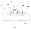
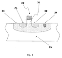
- Figs. 2 and 3 illustrate the difference between a thin-oxide transistor and a thick-oxide transistor.
- Fig. 2 shows a cross-sectional view of a substrate 25 supporting a well region 23. Within the well region 23 the source and drain (both denoted 22) are arranged. The gate 20 of the transistor is arranged on a thin oxide layer 21 which separates the gate 20 of the transistor with the well region 23. Contact 24 is provided for obtaining electrical contact to the well region 23.
- Fig. 3 shows a cross-sectional view of a substrate 35 supporting a well region 33.
- the source and drain both denoted 32
- the gate 30 of the transistor is arranged on a thick oxide layer 31 which separates the gate 30 of the transistor with the well region 33.
- the thickness of oxide-layer 31 is significantly larger than oxide layer 21.
- Gate oxide layer 31 has a thickness within the range 4-40 nm for example 13.5 nm for one suitable CMOS process whereas a typical thickness of gate oxide layer 21 is just a 3.6 nm in the same CMOS process.
- Contact 34 is provided for obtaining electrical contact to the well region 33.
- the substrate of the die is usually low-doped silicon (P- or N-type).
- the well regions are usually the same silicon-base material (P- or N-type) but doped with higher levels.
- the gate material is typically poly-silicon and the gate oxide is nitrided silicon-dioxide ('oxy-nitride').
- Circuit die dimensions are typically within the range 0.01 - 25 mm 2 .
- the transistor footprint on die is typically within the range 100 - 1000000 ⁇ m 2 .
Landscapes
- Engineering & Computer Science (AREA)
- Power Engineering (AREA)
- Multimedia (AREA)
- Microelectronics & Electronic Packaging (AREA)
- Physics & Mathematics (AREA)
- Acoustics & Sound (AREA)
- Signal Processing (AREA)
- Metal-Oxide And Bipolar Metal-Oxide Semiconductor Integrated Circuits (AREA)
- Amplifiers (AREA)
- Circuit For Audible Band Transducer (AREA)
- Bipolar Transistors (AREA)
Abstract
Description
- The present invention relates to an integrated circuit die and a condenser microphone assembly comprising such integrated circuit die. The integrated circuit die is fabricated in a deep sub-micron MOS technology and it comprises a preamplifier comprising an input stage comprising a thick-oxide MOS transistor.
- Modern MOS, in particular CMOS, integrated circuit fabrication technologies advance with ever shrinking device geometries to allow an increasing density of active elements, such as transistors. However, the shrinking of geometries puts among other things, severe limitation on allowable maximum voltages in the circuits so as to avoid for example gate oxide destructive breakdown in transistors. One way of overcoming these limitations in certain cases, is to offer so-called thick-oxide transistor devices suitable for higher voltage operation. Thus, by increasing the thickness of the gate oxide layer, a transistor can be operated at a relatively high voltage potential.
- Various documents within the technical field of electronics incorporating amplifiers and/or buffers suitable for processing signals generated by electro-acoustic transducers can be found in the patent literature. Examples of such documents are
WO 02/073792 US 2004/0202345 ,US 2005/0151589 ,US 2007/0009111 ,US 7,149,317 andEP 1 599 067 - A less appreciated characteristic of deep sub-micron CMOS technologies is the use of oxy-nitrides to realize very thin gate oxides needed for typical thin-oxide transistors. For deep sub-micron technologies with a minimum feature size below 0.35 micron oxy-nitrides replace conventional silicon oxide as the gate oxide material of choice. A significant disadvantage of using oxy-nitrides is a dramatic increase in transistor flicker noise arising from an increased carrier trap density found in oxy-nitride gate materials. As thin-oxide transistors as a consequence of the thin gate oxide at the same time exhibit a much higher capacitance per unit gate area the noise performance of certain types of preamplifiers, in particular preamplifiers suitable for capacitive transducers, such as miniature condenser microphones and miniature electric microphones, may suffer dramatically.
- Thus, an object of the present invention may be seen as to provide a MOS transistor-based preamplifier with a low-noise input stage realized in a deep sub-micron MOS technology, the MOS transistor-based low-noise input stage featuring a very low flicker noise level.
- The above-mentioned object is complied with by providing, in a first aspect, a deep sub-micron MOS integrated circuit die comprising a preamplifier comprising a first signal input terminal for receipt of electrical signals generated by an associated electro-acoustical transducer, said first signal input terminal being operatively coupled to an input stage of the preamplifier, said input stage comprising a thick-oxide transistor.
- By the term "input stage" is meant the amplifying or buffering transistor device of the preamplifier closest to a signal input terminal adapted to receive a signal or signals from the associated electrical transducer, such as a condenser microphone transducer or cartridge.
- As a thick-oxide transistor exhibits a low gate capacitance per unit gate area, and since flicker noise is known to be reduced by increasing the gate dimensions of the transistor, thick-oxide transistors with increased gate dimension may advantageously be used to amplify or buffer signals from for example capacitive microphone transducers, such as condenser microphone transducers or cartridges having source capacitances within the range 0.5-10 pF. Noise optimum coupling may often be achieved when the source/generator capacitance is close to the input capacitance of the first stage in the amplifier or buffer.
- The thickness of a gate oxide of the thick-oxide transistor may be within the range 4-40 nm, such as within the range 8-20 nm, such as approximately 13.5 nm.
- The thick-oxide transistor may comprise a P-type or N-type MOS transistor having a gate capacitance appropriately matched to the transducer or source capacitance. Thus, for miniature condenser microphone transducer or cartridges, an input capacitance of the first signal input terminal may be less than 50 pF, such as less than 40 pF, such as less than 30 pF, such as less than 10 pF, such as less than 5 pF. Similarly, an input impedance of the first signal input terminal may be larger than 10 GΩ, such as larger than 50 GΩ, such as larger than 100 GΩ, or even more preferably larger than 1000 GΩ.
- The thick-oxide transistor of the deep sub-micron MOS integrated circuit die may have a gate capacitance within the range 0.5-10 pF, such as within the range 1-8 pF, or even more preferably within the range 2-6 pF.
- In one embodiment of the invention, particularly well-suited for coupling to a MEMS microphone transducer with a generator capacitance of about 5-6 pF, gate dimensions (W/L) of the PMOS input transistor of the preamplifier is chosen to 600 µm /1 µm.
- The preamplifier may further comprise a second signal input terminal operatively coupled to a source input of the P-type MOS transistor, while the first signal input terminal may be operatively coupled to a gate input of the P-type or N-type MOS transistor. The first and second signal input terminals are operatively connectable to associated diaphragm and back-plate members, respectively, of the associated condenser microphone transducer. In another embodiment of the invention the preamplifier comprises a differential input stage that comprises a pair of thick-oxide NMOS or PMOS transistors.
- The first signal input terminal of the deep sub-micron MOS integrated circuit die may be coupled to the thick-oxide transistor via a DC blocking capacitor. The DC blocking capacitor may have a capacitance within the range 5-500 pF.
- In addition, the deep sub-micron MOS integrated circuit die may further comprise a microphone bias voltage source adapted to provide a predetermined DC bias voltage between a pair of terminals of the deep sub-micron MOS integrated circuit die so as to provide a DC bias voltage between the associated diaphragm and back-plate members. The microphone bias voltage source may provide the DC bias voltage to the first signal input terminal which may be connected to a high-impedance element ensuring the before-mentioned input impedance of 10-1000 GΩ, or even higher. The high-impedance element may comprise one or more resistors, one or more diode coupled transistors or one or more pairs of reversed biased semiconductor diodes. The bias voltage may be in the range 4-10 V.
- The deep sub-micron MOS integrated circuit die may further comprise a voltage regulator adapted to provide a regulated DC voltage, the voltage regulator being operatively coupled to the source input of the P-type or N-type MOS transistor.
- The deep sub-micron MOS integrated circuit die according to the first aspect of the present invention may exhibit a A-weighted input referred noise, referred to the first signal input terminal, being less than 2 µV RMS, such as less than 1 µV RMS. Similarly, a flicker noise corner of an input referred noise voltage density may be less than 1 kHz, such as less than 500 Hz, such as less than 100 Hz.
- The gate oxide of the thick-oxide transistor may comprise nitrided silicon-dioxide.
- In a second aspect, the present invention relates to a condenser microphone assembly comprising a condenser microphone transducer comprising adjacently positioned diaphragm and back-plate members having an air gap there between, and a deep sub-micron MOS integrated circuit die comprising a preamplifier comprising a first signal input terminal for receipt of electrical signals generated by the condenser microphone transducer, said first signal input terminal being operatively coupled to an input stage of the preamplifier, said input stage comprising a thick-oxide transistor.
- The condenser microphone transducer may have a transducer capacitance between 0.5 and 10 pF. The condenser microphone transducer may comprise a MEMS microphone transducer, such as a silicon-based transducer comprising a displaceable diaphragm and a back-plate having air ventilation channels arranged therein. The displaceable diaphragm may be highly electrically conductive to allow it to electrically shield the bulk of the condenser microphone from significant capacitive coupling to the back-plate.
- The condenser microphone assembly may further comprise a microphone housing or casing having a sound input port acoustically connected to the condenser microphone transducer, preferably via an acoustical channel. In this way acoustical signals are guided from the exterior of the microphone housing or casing to the condenser microphone transducer. The acoustical channel extending from the sound inlet port to a sound inlet of the condenser microphone transducer may form an acoustical seal to the interior of the remaining volume of the microphone housing or casing. The microphone housing or casing may in addition comprise a plurality of externally accessible electrical terminals in order to provide electrical signals to and from the condenser microphone assembly. Such electrical signals may include power supply signals, output signals representing measured acoustical signals etc. The deep sub-micron MOS integrated circuit die may, preferably, be arranged inside the microphone housing or casing.
- The preamplifier may further comprise a second input terminal, wherein the first and second signal input terminals are operatively coupled to the diaphragm and back-plate members, respectively.
- The thick-oxide transistor of the preamplifier may comprise a P-type MOS transistor or N-type MOS transistor. The thickness of a gate oxide of the thick-oxide transistor may be within the range 4-40 nm, such as within the range 8-20 nm.
- The deep sub-micron MOS integrated circuit die may further comprise a microphone bias voltage source adapted to provide a predetermined DC bias voltage between a pair of terminals of the deep sub-micron MOS integrated circuit die. The bias voltage source may be adapted to provide a DC bias voltage within the range 4-10 V. The microphone bias voltage source may provide the DC bias voltage to the first signal input terminal which may be connected to a high-impedance element ensuring the before-mentioned input impedance of 10-1000 GΩ, or even higher. The high-impedance element may comprise one or more resistors, one or more diode coupled transistors or one or more pairs of reversed biased semiconductor diodes.
- Moreover, the first signal input terminal may be coupled to the thick-oxide transistor via a DC blocking capacitor. The DC blocking capacitor may have a capacitance within the range 5-500 pF.
- The first signal input terminal may have an input capacitance of less than 50 pF, such as less than 40 pF, such as less than 30 pF, such as less than 20 pF, such as less than 10 pF, such as less than 5 pF. Similarly, an input impedance of the first signal input terminal may be larger than 10 GΩ, such as larger than 50 GΩ, such as larger than 100 GΩ, or even more preferably larger than 1000 GΩ.
- A gate capacitance of the thick-oxide transistor may be within the range 0.5-10 pF, such as within the range 1-8 pF, or even more preferably within the range 2-6 pF.
- The deep sub-micron MOS integrated circuit die of the condenser microphone assembly may exhibit a A-weighted input referred noise, referred to the first signal input terminal, being less than 2 µV RMS, such as less than 1 µV RMS. Similarly, a flicker noise corner of an input referred noise voltage density may be less than 1 kHz, such as less than 500 Hz, such as less than 100 Hz.
- The gate oxide of the thick-oxide transistor may comprise nitrided silicon-dioxide.
- In a third aspect, the present invention relates to a portable communication device comprising a deep sub-micron MOS integrated circuit die according to the first aspect of the present invention, said portable communication device being selected from the group consisting of: cell phones, hearing aids, PDAs, game consoles, portable computers, and any combination thereof.
- In a fourth aspect, the present invention relates to a portable communication device comprising a condenser microphone assembly according to the second aspect of the present invention, said portable communication device being selected from the group consisting of: cell phones, hearing aids, PDAs, and any combination thereof.
- The present invention will now be explained in greater details with reference to the accompanying figures, within
-
Fig. 1 shows a simplified schematic of a microphone preamplifier input stage, -
Fig. 2 shows a cross-sectional view of a thin-oxide PMOS transistor, and -
Fig. 3 shows a cross-sectional view of a thick-oxide PMOS transistor. - While the invention is susceptible to various modifications and alternative forms, specific embodiments have been shown by way of example in the drawings and will be described in detail herein. It should be understood, however, that the invention is not intended to be limited to the particular forms disclosed. Rather, the invention is to cover all modifications, equivalents, and alternatives falling within the spirit and scope of the invention as defined by the appended claims.
- In its most general aspect the present invention relates to a deep sub-micron MOS, such as CMOS, integrated circuit die comprising a preamplifier. The preamplifier comprises a first signal input terminal for receipt of electrical transducer signals generated by for example condenser microphone transducers. The first signal input terminal is operatively coupled to an input stage of the preamplifier, said input stage comprising a thick-oxide transistor exhibiting superior properties in terms of flicker noise level and input capacitance.
-
Fig. 1 illustrates a silicon-based microphone assembly according to one embodiment of the present invention. A high impedance DCbias voltage source 1 for acondenser transducer element 3 and aDC blocking capacitor 5 are both integrated on the electronic or integrated semiconductor circuit die 6 together with an input stage thick-oxide P-typefield effect transistor 7, which preferably is a PMOS transistor, and anoptional voltage regulator 8. The high impedance DCbias voltage source 1 is shown schematically as a cascade of a DC bias voltage generator and a large series resistor. The high impedance DCbias voltage source 1 may in fact comprise a voltage pump or multiplier, such as Dickson voltage multiplier, utilizing a supply voltage (VDD) of the integrated circuit die 6 to generate a multiplied higher DC voltage. In one embodiment of the invention, a nominal supply voltage of 1.8 volt is multiplied to generate a high impedance DC bias voltage of about 8 volts. - The thick-
oxide PMOS transistor 7 references thevoltage supply node 14. Thevoltage supply node 14 may be derived directly from the external power supply voltage VDD of the microphone assembly, or alternatively, it may be derived by regulating and stabilizing the external supply voltage VDD by aregulator circuit 8. Theregulator circuit 8 provides the low output impedance required for coupling to thePMOS transistor 7 amplifying element. - The back-
plate terminal 13 and the diaphragm terminal 14 (also called voltage node) of thecondenser transducer element 3 are referenced to the same node as the input stage of the preamplifier. Supply noise on thevoltage supply node 14 is significantly attenuated because any signal on 14 will commonly be applied to the gate input of thePMOS transistor 7 of the microphone preamplifier and therefore not amplified. Furthermore, the input stage comprises the thick-oxide PMOS transistor 7, which often has superior flicker noise properties compared to a NMOS transistor. For this reason, both white noise and flicker noise of the input stage are reduced to a minimum. - The thick-
oxide PMOS transistor 7 preferably has a width (W) between 100 and 5000 µm and a length between 0.5 and 5 µm. The thickness of a gate oxide of the thick-oxide PMOS transistor 7 is usually within the range 4-40 nm for sub-micron CMOS processes and is determined by the selected semiconductor process. The gate capacitance of the PMOS transistor is preferably smaller than the condenser microphone transducer capacitance - for example about 10 pF. However, the gate capacitance can also be smaller, such as about 5 pF or even smaller. - The DC bias current is preferably set to a value between 10 pA and 100 pA for microphone assemblies targeted for battery-powered portable communication devices but other DC bias current values may be selected in other types of applications.
- As previously stated, a first externally
accessible terminal 13 and a second externallyaccessible terminal 14 are operatively coupled to the gate and source inputs, respectively, ofPMOS transistor 7. The first externallyaccessible terminal 13 is furthermore coupled to high impedance DCbias voltage source 1 to allow this externally accessible terminal to be electrically coupled to a back-plate 12 or adiaphragm 15 of an associatedcondenser transducer element 3. The gate input of thePMOS transistor 7 is electrically shielded from the DC bias voltage provided on the first externallyaccessible terminal 13 by theDC blocking capacitor 5 to allow setting the DC bias point of thePMOS transistor 7 through an independentbias setting network 2 comprising a pair of reverse biased diodes. Such a pair of reversed biased diodes ensures an input impedance higher than 100 GΩ of the input stage of the preamplifier. In fact, a pair of parallel diodes in reverse polarity may have an impedance of several TΩ. - In case the preamplifier is to be integrated in an ASIC, the pair of parallel diodes coupled in reverse polarity may advantageously be integrated therewith.
-
Figs. 2 and3 illustrate the difference between a thin-oxide transistor and a thick-oxide transistor.Fig. 2 shows a cross-sectional view of asubstrate 25 supporting awell region 23. Within thewell region 23 the source and drain (both denoted 22) are arranged. Thegate 20 of the transistor is arranged on athin oxide layer 21 which separates thegate 20 of the transistor with thewell region 23.Contact 24 is provided for obtaining electrical contact to thewell region 23. -
Fig. 3 shows a cross-sectional view of asubstrate 35 supporting awell region 33. Within thewell region 33 the source and drain (both denoted 32) are arranged. Thegate 30 of the transistor is arranged on athick oxide layer 31 which separates thegate 30 of the transistor with thewell region 33. Compared toFig. 2 the thickness of oxide-layer 31 is significantly larger thanoxide layer 21.Gate oxide layer 31 has a thickness within the range 4-40 nm for example 13.5 nm for one suitable CMOS process whereas a typical thickness ofgate oxide layer 21 is just a 3.6 nm in the same CMOS process.Contact 34 is provided for obtaining electrical contact to thewell region 33. - The substrate of the die is usually low-doped silicon (P- or N-type). The well regions are usually the same silicon-base material (P- or N-type) but doped with higher levels. The gate material is typically poly-silicon and the gate oxide is nitrided silicon-dioxide ('oxy-nitride').
- Circuit die dimensions are typically within the range 0.01 - 25 mm2. The transistor footprint on die is typically within the range 100 - 1000000 µm2.
Claims (31)
- A condenser microphone assembly comprising:- a condenser microphone transducer comprising adjacently positioned diaphragm and back-plate members having an air gap there between,- a deep sub-micron MOS integrated circuit die comprising a preamplifier comprising a first signal input terminal for receipt of electrical signals generated by the condenser microphone transducer, said first signal input terminal being operatively coupled to an input stage of the preamplifier, said input stage comprising a thick-oxide transistor.
- A condenser microphone assembly according to claim 1, wherein the condenser microphone transducer comprises a MEMS microphone transducer.
- A condenser microphone assembly according to claim 1 or 2, further comprising a microphone housing having- a sound input port acoustically connected to the condenser microphone transducer, and- a plurality of externally accessible electrical terminals,wherein the deep sub-micron MOS integrated circuit die is arranged inside the microphone housing.
- A condenser microphone assembly according to any of claims 1-3, wherein the condenser microphone transducer has a transducer capacitance within the range 0.5-10 pF.
- A condenser microphone assembly according to any of claims 1-4, wherein the preamplifier further comprises a second input terminal, and wherein the first and second signal input terminals are operatively coupled to the diaphragm and back-plate members, respectively.
- A condenser microphone assembly according to any of the preceding claims, wherein the thick-oxide transistor of the preamplifier comprises a P-type MOS transistor or N-type MOS transistor.
- A condenser microphone assembly according to claim 6, wherein the deep sub-micron MOS integrated circuit die further comprises a microphone bias voltage source adapted to provide a predetermined DC bias voltage between a pair of terminals of the deep sub-micron MOS integrated circuit die.
- A condenser microphone according to claim 7, wherein the bias voltage source is adapted to provide a DC bias voltage within the range 4-10 V.
- A condenser microphone assembly according to claim 7 or 8, wherein the bias voltage source is adapted to provide the DC bias voltage to the first signal input terminal.
- A condenser microphone assembly according to any of the preceding claims, wherein the first signal input terminal is coupled to the thick-oxide transistor via a DC blocking capacitor.
- A condenser microphone assembly according to any of the preceding claims, wherein an input capacitance of the first signal input terminal is less than 50 pF, such as less than 40 pF, such as less than 30 pF, such as less than 20 pF, such as less than 10 pF, such as less than 5 pF.
- A condenser microphone assembly according to any of the preceding claims, wherein an input impedance at the first signal input terminal is larger than 10 GΩ, such as larger than 50 GΩ, such as larger than 100 GΩ, or even more preferably larger than 1000 GΩ.
- A condenser microphone assembly according to any of the preceding claims, wherein a gate capacitance of the thick-oxide transistor is within the range 0.5-10 pF, such as within the range 1-8 pF, or even more preferably within the range 2-6 pF.
- A condenser microphone assembly according to any of the preceding claims, wherein a A-weighted input referred noise, referred to the first signal input terminal, is less than 2 µV RMS, such as less than 1 µV RMS.
- A condenser microphone assembly according to any of the preceding claims, wherein a flicker noise corner of an input referred noise voltage density is less than 1 kHz, such as less than 500 Hz, such as less than 100 Hz.
- A condenser microphone assembly according to any of the preceding claims, wherein a thickness of a gate oxide of the thick-oxide transistor is within the range 4-40 nm, such as within the range 8-20 nm.
- A condenser microphone assembly according to any of the preceding claims, wherein a gate oxide of the thick-oxide transistor comprises nitrided silicon-dioxide.
- A deep sub-micron MOS integrated circuit die comprising a preamplifier comprising a first signal input terminal for receipt of electrical signals generated by an associated electro-acoustical transducer, said first signal input terminal being operatively coupled to an input stage of the preamplifier, said input stage comprising a thick-oxide transistor.
- A deep sub-micron MOS integrated circuit die according to claim 18, wherein the thick-oxide transistor comprises a P-type MOS transistor or N-type MOS transistor.
- A deep sub-micron MOS integrated circuit die according to claim 18 or 19, wherein the deep sub-micron MOS integrated circuit die further comprises a microphone bias voltage source adapted to provide a predetermined DC bias voltage between a pair of terminals of the deep sub-micron MOS integrated circuit die.
- A deep submicron MOS integrated circuit die according to claim 20, wherein bias voltage source is adapted to provide a DC bias voltage within the range 4-10 V.
- A deep sub-micron MOS integrated circuit die according to claim 20 or 21, wherein the bias voltage source is adapted to provide the DC bias voltage to the first signal input terminal.
- A deep sub-micron MOS integrated circuit die according to any of claims 18-22, wherein the first signal input terminal is coupled to the thick-oxide transistor via a DC blocking capacitor.
- A deep sub-micron MOS integrated circuit die according to any of claims 18-23, wherein an input capacitance of the first signal input terminal is less than 50 pF, such as less than 40 pF, such as less than 30 pF, such as less than 20 pF, such as less than 10 pF, such as less than 5 pF.
- A deep sub-micron MOS integrated circuit die according to any of claims 18-24, wherein an input impedance at the first signal input terminal is larger than 10 GΩ, such as larger than 50 GΩ, such as larger than 100 GΩ, or even more preferably larger than 1000 GΩ.
- A deep sub-micron MOS integrated circuit die according to any of claims 18-25, wherein a gate capacitance of the thick-oxide transistor is within the range 0.5-10 pF, such as within the range 1-8 pF, or even more preferably within the range 2-6 pF.
- A deep sub-micron MOS integrated circuit die according to any of claims 18-26, wherein a A-weighted input referred noise, referred to the first signal input terminal, is less than 2 µV RMS, such as less than 1 µV RMS.
- A deep sub-micron MOS integrated circuit die according to any of claims 18-27, wherein a flicker noise corner of an input referred noise voltage density is less than 1 kHz, such as less than 500 Hz, such as less than 100 Hz.
- A deep sub-micron MOS integrated circuit die according to any of claims 18-28, wherein a thickness of a gate oxide of the thick-oxide transistor is within the range 4-40 nm, such as within the range 8-20 nm.
- A deep sub-micron MOS integrated circuit die according to any of claims 18-29, wherein a gate oxide of the thick-oxide transistor comprises nitrided silicon-dioxide.
- A portable communication device comprising a deep sub-micron MOS integrated circuit die according to any of claims 18-30, said portable communication device being selected from the group consisting of: cell phones, hearing aids, PDAs, game consoles, portable computers, and any combination thereof.
Applications Claiming Priority (1)
| Application Number | Priority Date | Filing Date | Title |
|---|---|---|---|
| US87545206P | 2006-12-18 | 2006-12-18 |
Publications (2)
| Publication Number | Publication Date |
|---|---|
| EP1936689A1 true EP1936689A1 (en) | 2008-06-25 |
| EP1936689B1 EP1936689B1 (en) | 2012-03-14 |
Family
ID=38529830
Family Applications (1)
| Application Number | Title | Priority Date | Filing Date |
|---|---|---|---|
| EP07150087A Active EP1936689B1 (en) | 2006-12-18 | 2007-12-18 | Deep sub-micron MOS preamplifier with thick-oxide input stage transistor |
Country Status (5)
| Country | Link |
|---|---|
| US (1) | US8094846B2 (en) |
| EP (1) | EP1936689B1 (en) |
| KR (1) | KR101485067B1 (en) |
| CN (1) | CN101287304B (en) |
| AT (1) | ATE549794T1 (en) |
Families Citing this family (10)
| Publication number | Priority date | Publication date | Assignee | Title |
|---|---|---|---|---|
| US8542850B2 (en) | 2007-09-12 | 2013-09-24 | Epcos Pte Ltd | Miniature microphone assembly with hydrophobic surface coating |
| DE102007058951B4 (en) * | 2007-12-07 | 2020-03-26 | Snaptrack, Inc. | MEMS package |
| ITTO20090495A1 (en) | 2009-06-30 | 2011-01-01 | St Microelectronics Srl | PREAMPLIFIER CIRCUIT FOR A CAPACITIVE MICRO-ELECTROMECHANICAL ACOUSTIC TRANSDUCER |
| DE102010006132B4 (en) | 2010-01-29 | 2013-05-08 | Epcos Ag | Miniaturized electrical component with a stack of a MEMS and an ASIC |
| US9181086B1 (en) | 2012-10-01 | 2015-11-10 | The Research Foundation For The State University Of New York | Hinged MEMS diaphragm and method of manufacture therof |
| US9331655B2 (en) * | 2013-07-10 | 2016-05-03 | Broadcom Corporation | Pop-click noise grounding switch design with deep sub-micron CMOS technology |
| US9608437B2 (en) * | 2013-09-12 | 2017-03-28 | Qualcomm Incorporated | Electro-static discharge protection for integrated circuits |
| WO2017136364A1 (en) * | 2016-02-01 | 2017-08-10 | Knowles Electronics, Llc | Apparatus to bias mems motors |
| US12091313B2 (en) | 2019-08-26 | 2024-09-17 | The Research Foundation For The State University Of New York | Electrodynamically levitated actuator |
| CN112290899B (en) * | 2020-10-26 | 2024-02-06 | 杭州爱华仪器有限公司 | Preamplifier of measuring circuit |
Citations (8)
| Publication number | Priority date | Publication date | Assignee | Title |
|---|---|---|---|---|
| WO2001091280A1 (en) * | 2000-05-22 | 2001-11-29 | Microtronic Nederland B.V. | High impedance bias device |
| EP1233451A2 (en) * | 2001-02-20 | 2002-08-21 | Programmable Silicon Solutions | Integrated radio frequency circuit devices |
| WO2002073792A2 (en) * | 2001-03-09 | 2002-09-19 | Techtronic A/S | An electret condensor microphone preamplifier that is insensitive to leakage currents at the input |
| US6642543B1 (en) * | 2000-09-26 | 2003-11-04 | The Board Of Trustees Of The Leland Stanford Junior University | Thin and thick gate oxide transistors on a functional block of a CMOS circuit residing within the core of an IC chip |
| US20040085137A1 (en) * | 2002-08-27 | 2004-05-06 | Furst Claus Erdmann | Preamplifier for two terminal electret condenser microphones |
| WO2004057909A2 (en) * | 2002-12-20 | 2004-07-08 | Sonion Lyngby A/S | Silicon-based transducer for use in hearing instruments |
| WO2005011108A2 (en) * | 2003-07-17 | 2005-02-03 | Massachusetts Institute Of Technology | Low-power high-psrr current-mode microphone pre-amplifier system and method |
| WO2005055406A1 (en) * | 2003-12-01 | 2005-06-16 | Audioasics A/S | Microphine with voltage pump |
Family Cites Families (14)
| Publication number | Priority date | Publication date | Assignee | Title |
|---|---|---|---|---|
| JPH03196677A (en) | 1989-12-26 | 1991-08-28 | Nec Corp | Semiconductor device |
| JP2001102875A (en) | 1999-10-01 | 2001-04-13 | Hosiden Corp | Semiconductor amplifier circuit and semiconductor electret condenser microphone |
| US6181193B1 (en) * | 1999-10-08 | 2001-01-30 | International Business Machines Corporation | Using thick-oxide CMOS devices to interface high voltage integrated circuits |
| SE522714C2 (en) | 2001-07-13 | 2004-03-02 | Ericsson Telefon Ab L M | Preparation of low noise MOS device |
| JP2003179071A (en) * | 2001-10-25 | 2003-06-27 | Sharp Corp | Method of fabricating deep submicron CMOS source / drain using MDD and selective CVD silicide |
| JP2003230195A (en) * | 2002-02-06 | 2003-08-15 | Hosiden Corp | Electret condenser microphone |
| CN1280881C (en) * | 2002-03-25 | 2006-10-18 | 华邦电子股份有限公司 | Deep infra micro MOS devices and its manufacturing method |
| US7149317B2 (en) * | 2002-04-18 | 2006-12-12 | Sonionmicrotronic Nederland B.V. | CMOS high impedance circuit |
| US7466835B2 (en) * | 2003-03-18 | 2008-12-16 | Sonion A/S | Miniature microphone with balanced termination |
| US6977543B2 (en) * | 2003-08-26 | 2005-12-20 | Intel Corporation | Biasing technique using thin and thick oxide transistors |
| ATE410820T1 (en) * | 2004-01-12 | 2008-10-15 | Sonion As | AMPLIFIER CIRCUIT FOR CAPACITIVE CONVERTERS |
| EP1599067B1 (en) | 2004-05-21 | 2013-05-01 | Epcos Pte Ltd | Detection and control of diaphragm collapse in condenser microphones |
| US7271651B2 (en) * | 2005-06-17 | 2007-09-18 | Agere Systems Inc. | High performance differential amplifiers with thick oxide devices for high impedance nodes |
| EP1742506B1 (en) * | 2005-07-06 | 2013-05-22 | Epcos Pte Ltd | Microphone assembly with P-type preamplifier input stage |
-
2007
- 2007-12-17 CN CN2007101857943A patent/CN101287304B/en not_active Expired - Fee Related
- 2007-12-17 US US11/958,103 patent/US8094846B2/en active Active
- 2007-12-18 EP EP07150087A patent/EP1936689B1/en active Active
- 2007-12-18 AT AT07150087T patent/ATE549794T1/en active
- 2007-12-18 KR KR20070133653A patent/KR101485067B1/en not_active Expired - Fee Related
Patent Citations (8)
| Publication number | Priority date | Publication date | Assignee | Title |
|---|---|---|---|---|
| WO2001091280A1 (en) * | 2000-05-22 | 2001-11-29 | Microtronic Nederland B.V. | High impedance bias device |
| US6642543B1 (en) * | 2000-09-26 | 2003-11-04 | The Board Of Trustees Of The Leland Stanford Junior University | Thin and thick gate oxide transistors on a functional block of a CMOS circuit residing within the core of an IC chip |
| EP1233451A2 (en) * | 2001-02-20 | 2002-08-21 | Programmable Silicon Solutions | Integrated radio frequency circuit devices |
| WO2002073792A2 (en) * | 2001-03-09 | 2002-09-19 | Techtronic A/S | An electret condensor microphone preamplifier that is insensitive to leakage currents at the input |
| US20040085137A1 (en) * | 2002-08-27 | 2004-05-06 | Furst Claus Erdmann | Preamplifier for two terminal electret condenser microphones |
| WO2004057909A2 (en) * | 2002-12-20 | 2004-07-08 | Sonion Lyngby A/S | Silicon-based transducer for use in hearing instruments |
| WO2005011108A2 (en) * | 2003-07-17 | 2005-02-03 | Massachusetts Institute Of Technology | Low-power high-psrr current-mode microphone pre-amplifier system and method |
| WO2005055406A1 (en) * | 2003-12-01 | 2005-06-16 | Audioasics A/S | Microphine with voltage pump |
Also Published As
| Publication number | Publication date |
|---|---|
| KR101485067B1 (en) | 2015-01-21 |
| ATE549794T1 (en) | 2012-03-15 |
| US8094846B2 (en) | 2012-01-10 |
| EP1936689B1 (en) | 2012-03-14 |
| CN101287304A (en) | 2008-10-15 |
| CN101287304B (en) | 2013-02-06 |
| US20080152171A1 (en) | 2008-06-26 |
| KR20080056683A (en) | 2008-06-23 |
Similar Documents
| Publication | Publication Date | Title |
|---|---|---|
| EP1936689B1 (en) | Deep sub-micron MOS preamplifier with thick-oxide input stage transistor | |
| EP1742506B1 (en) | Microphone assembly with P-type preamplifier input stage | |
| CN102224675B (en) | Dynamically biased amplifier | |
| CN105024653B (en) | Low-noise amplifier for MEMS capacitive transducer | |
| US20090086992A1 (en) | Microphone circuit and charge amplifier thereof | |
| US8774428B2 (en) | Very low power MEMS microphone | |
| US8139790B2 (en) | Integrated circuit biasing a microphone | |
| US20080192962A1 (en) | Microphone with dual transducers | |
| US9455671B2 (en) | System and method for capacitive signal source amplifier | |
| US20040085137A1 (en) | Preamplifier for two terminal electret condenser microphones | |
| WO2007108929A2 (en) | Two-wire microphone circuit | |
| US10582309B2 (en) | MEMS transducer amplifiers | |
| US8059836B2 (en) | Microphone bias circuits | |
| US20230262382A1 (en) | Readout circuit for microphone sensor | |
| JP2005204297A (en) | Amplification device with bias circuit | |
| JP2006245740A (en) | Amplifier circuit and electret condenser microphone using the same | |
| US20200344557A1 (en) | Microphone assembly with improved overload performance | |
| JP2005109842A (en) | Amplifier circuit for condenser microphone | |
| US20250226800A1 (en) | Amplifier circuit for microphone, microphone circuit and electronic device | |
| JP2019205000A (en) | Charge detection circuit and piezoelectric microphone | |
| CN101401451A (en) | Two-wire microphone circuit | |
| CN120345180A (en) | Low Noise Amplifier | |
| GB2627020A (en) | Low noise amplifier |
Legal Events
| Date | Code | Title | Description |
|---|---|---|---|
| PUAI | Public reference made under article 153(3) epc to a published international application that has entered the european phase |
Free format text: ORIGINAL CODE: 0009012 |
|
| AK | Designated contracting states |
Kind code of ref document: A1 Designated state(s): AT BE BG CH CY CZ DE DK EE ES FI FR GB GR HU IE IS IT LI LT LU LV MC MT NL PL PT RO SE SI SK TR |
|
| AX | Request for extension of the european patent |
Extension state: AL BA HR MK RS |
|
| 17P | Request for examination filed |
Effective date: 20081229 |
|
| AKX | Designation fees paid |
Designated state(s): AT BE BG CH CY CZ DE DK EE ES FI FR GB GR HU IE IS IT LI LT LU LV MC MT NL PL PT RO SE SI SK TR |
|
| 17Q | First examination report despatched |
Effective date: 20091204 |
|
| RAP1 | Party data changed (applicant data changed or rights of an application transferred) |
Owner name: EPCOS PTE LTD |
|
| REG | Reference to a national code |
Ref country code: DE Ref legal event code: R079 Ref document number: 602007021275 Country of ref document: DE Free format text: PREVIOUS MAIN CLASS: H01L0027088000 Ipc: H03F0003187000 |
|
| GRAP | Despatch of communication of intention to grant a patent |
Free format text: ORIGINAL CODE: EPIDOSNIGR1 |
|
| RIC1 | Information provided on ipc code assigned before grant |
Ipc: H01L 27/088 20060101ALI20110922BHEP Ipc: H03F 3/187 20060101AFI20110922BHEP Ipc: H04R 1/00 20060101ALI20110922BHEP Ipc: H03F 1/56 20060101ALI20110922BHEP Ipc: H01L 21/8234 20060101ALI20110922BHEP Ipc: H04R 3/00 20060101ALI20110922BHEP Ipc: H03F 1/52 20060101ALI20110922BHEP Ipc: H03F 3/185 20060101ALI20110922BHEP |
|
| GRAS | Grant fee paid |
Free format text: ORIGINAL CODE: EPIDOSNIGR3 |
|
| GRAA | (expected) grant |
Free format text: ORIGINAL CODE: 0009210 |
|
| RIN1 | Information on inventor provided before grant (corrected) |
Inventor name: STENBERG, LARS JORN Inventor name: HOVESTEN, PER F. |
|
| AK | Designated contracting states |
Kind code of ref document: B1 Designated state(s): AT BE BG CH CY CZ DE DK EE ES FI FR GB GR HU IE IS IT LI LT LU LV MC MT NL PL PT RO SE SI SK TR |
|
| REG | Reference to a national code |
Ref country code: GB Ref legal event code: FG4D |
|
| REG | Reference to a national code |
Ref country code: CH Ref legal event code: EP Ref country code: AT Ref legal event code: REF Ref document number: 549794 Country of ref document: AT Kind code of ref document: T Effective date: 20120315 |
|
| REG | Reference to a national code |
Ref country code: IE Ref legal event code: FG4D |
|
| REG | Reference to a national code |
Ref country code: DE Ref legal event code: R096 Ref document number: 602007021275 Country of ref document: DE Effective date: 20120510 |
|
| REG | Reference to a national code |
Ref country code: NL Ref legal event code: VDEP Effective date: 20120314 |
|
| PG25 | Lapsed in a contracting state [announced via postgrant information from national office to epo] |
Ref country code: LT Free format text: LAPSE BECAUSE OF FAILURE TO SUBMIT A TRANSLATION OF THE DESCRIPTION OR TO PAY THE FEE WITHIN THE PRESCRIBED TIME-LIMIT Effective date: 20120314 |
|
| LTIE | Lt: invalidation of european patent or patent extension |
Effective date: 20120314 |
|
| PG25 | Lapsed in a contracting state [announced via postgrant information from national office to epo] |
Ref country code: FI Free format text: LAPSE BECAUSE OF FAILURE TO SUBMIT A TRANSLATION OF THE DESCRIPTION OR TO PAY THE FEE WITHIN THE PRESCRIBED TIME-LIMIT Effective date: 20120314 Ref country code: LV Free format text: LAPSE BECAUSE OF FAILURE TO SUBMIT A TRANSLATION OF THE DESCRIPTION OR TO PAY THE FEE WITHIN THE PRESCRIBED TIME-LIMIT Effective date: 20120314 Ref country code: GR Free format text: LAPSE BECAUSE OF FAILURE TO SUBMIT A TRANSLATION OF THE DESCRIPTION OR TO PAY THE FEE WITHIN THE PRESCRIBED TIME-LIMIT Effective date: 20120615 |
|
| REG | Reference to a national code |
Ref country code: AT Ref legal event code: MK05 Ref document number: 549794 Country of ref document: AT Kind code of ref document: T Effective date: 20120314 |
|
| PG25 | Lapsed in a contracting state [announced via postgrant information from national office to epo] |
Ref country code: CY Free format text: LAPSE BECAUSE OF FAILURE TO SUBMIT A TRANSLATION OF THE DESCRIPTION OR TO PAY THE FEE WITHIN THE PRESCRIBED TIME-LIMIT Effective date: 20120314 |
|
| PG25 | Lapsed in a contracting state [announced via postgrant information from national office to epo] |
Ref country code: SE Free format text: LAPSE BECAUSE OF FAILURE TO SUBMIT A TRANSLATION OF THE DESCRIPTION OR TO PAY THE FEE WITHIN THE PRESCRIBED TIME-LIMIT Effective date: 20120314 Ref country code: CZ Free format text: LAPSE BECAUSE OF FAILURE TO SUBMIT A TRANSLATION OF THE DESCRIPTION OR TO PAY THE FEE WITHIN THE PRESCRIBED TIME-LIMIT Effective date: 20120314 Ref country code: EE Free format text: LAPSE BECAUSE OF FAILURE TO SUBMIT A TRANSLATION OF THE DESCRIPTION OR TO PAY THE FEE WITHIN THE PRESCRIBED TIME-LIMIT Effective date: 20120314 Ref country code: RO Free format text: LAPSE BECAUSE OF FAILURE TO SUBMIT A TRANSLATION OF THE DESCRIPTION OR TO PAY THE FEE WITHIN THE PRESCRIBED TIME-LIMIT Effective date: 20120314 Ref country code: SI Free format text: LAPSE BECAUSE OF FAILURE TO SUBMIT A TRANSLATION OF THE DESCRIPTION OR TO PAY THE FEE WITHIN THE PRESCRIBED TIME-LIMIT Effective date: 20120314 Ref country code: PL Free format text: LAPSE BECAUSE OF FAILURE TO SUBMIT A TRANSLATION OF THE DESCRIPTION OR TO PAY THE FEE WITHIN THE PRESCRIBED TIME-LIMIT Effective date: 20120314 Ref country code: IS Free format text: LAPSE BECAUSE OF FAILURE TO SUBMIT A TRANSLATION OF THE DESCRIPTION OR TO PAY THE FEE WITHIN THE PRESCRIBED TIME-LIMIT Effective date: 20120714 Ref country code: BE Free format text: LAPSE BECAUSE OF FAILURE TO SUBMIT A TRANSLATION OF THE DESCRIPTION OR TO PAY THE FEE WITHIN THE PRESCRIBED TIME-LIMIT Effective date: 20120314 |
|
| PG25 | Lapsed in a contracting state [announced via postgrant information from national office to epo] |
Ref country code: PT Free format text: LAPSE BECAUSE OF FAILURE TO SUBMIT A TRANSLATION OF THE DESCRIPTION OR TO PAY THE FEE WITHIN THE PRESCRIBED TIME-LIMIT Effective date: 20120716 Ref country code: SK Free format text: LAPSE BECAUSE OF FAILURE TO SUBMIT A TRANSLATION OF THE DESCRIPTION OR TO PAY THE FEE WITHIN THE PRESCRIBED TIME-LIMIT Effective date: 20120314 |
|
| PLBE | No opposition filed within time limit |
Free format text: ORIGINAL CODE: 0009261 |
|
| STAA | Information on the status of an ep patent application or granted ep patent |
Free format text: STATUS: NO OPPOSITION FILED WITHIN TIME LIMIT |
|
| PG25 | Lapsed in a contracting state [announced via postgrant information from national office to epo] |
Ref country code: NL Free format text: LAPSE BECAUSE OF FAILURE TO SUBMIT A TRANSLATION OF THE DESCRIPTION OR TO PAY THE FEE WITHIN THE PRESCRIBED TIME-LIMIT Effective date: 20120314 Ref country code: DK Free format text: LAPSE BECAUSE OF FAILURE TO SUBMIT A TRANSLATION OF THE DESCRIPTION OR TO PAY THE FEE WITHIN THE PRESCRIBED TIME-LIMIT Effective date: 20120314 Ref country code: AT Free format text: LAPSE BECAUSE OF FAILURE TO SUBMIT A TRANSLATION OF THE DESCRIPTION OR TO PAY THE FEE WITHIN THE PRESCRIBED TIME-LIMIT Effective date: 20120314 |
|
| 26N | No opposition filed |
Effective date: 20121217 |
|
| PG25 | Lapsed in a contracting state [announced via postgrant information from national office to epo] |
Ref country code: IT Free format text: LAPSE BECAUSE OF FAILURE TO SUBMIT A TRANSLATION OF THE DESCRIPTION OR TO PAY THE FEE WITHIN THE PRESCRIBED TIME-LIMIT Effective date: 20120314 |
|
| REG | Reference to a national code |
Ref country code: DE Ref legal event code: R097 Ref document number: 602007021275 Country of ref document: DE Effective date: 20121217 |
|
| PG25 | Lapsed in a contracting state [announced via postgrant information from national office to epo] |
Ref country code: ES Free format text: LAPSE BECAUSE OF FAILURE TO SUBMIT A TRANSLATION OF THE DESCRIPTION OR TO PAY THE FEE WITHIN THE PRESCRIBED TIME-LIMIT Effective date: 20120625 |
|
| PG25 | Lapsed in a contracting state [announced via postgrant information from national office to epo] |
Ref country code: BG Free format text: LAPSE BECAUSE OF FAILURE TO SUBMIT A TRANSLATION OF THE DESCRIPTION OR TO PAY THE FEE WITHIN THE PRESCRIBED TIME-LIMIT Effective date: 20120614 Ref country code: MC Free format text: LAPSE BECAUSE OF NON-PAYMENT OF DUE FEES Effective date: 20121231 |
|
| REG | Reference to a national code |
Ref country code: CH Ref legal event code: PL |
|
| REG | Reference to a national code |
Ref country code: IE Ref legal event code: MM4A |
|
| REG | Reference to a national code |
Ref country code: FR Ref legal event code: ST Effective date: 20130830 |
|
| PG25 | Lapsed in a contracting state [announced via postgrant information from national office to epo] |
Ref country code: LI Free format text: LAPSE BECAUSE OF NON-PAYMENT OF DUE FEES Effective date: 20121231 Ref country code: CH Free format text: LAPSE BECAUSE OF NON-PAYMENT OF DUE FEES Effective date: 20121231 Ref country code: IE Free format text: LAPSE BECAUSE OF NON-PAYMENT OF DUE FEES Effective date: 20121218 |
|
| PG25 | Lapsed in a contracting state [announced via postgrant information from national office to epo] |
Ref country code: FR Free format text: LAPSE BECAUSE OF NON-PAYMENT OF DUE FEES Effective date: 20130102 Ref country code: MT Free format text: LAPSE BECAUSE OF FAILURE TO SUBMIT A TRANSLATION OF THE DESCRIPTION OR TO PAY THE FEE WITHIN THE PRESCRIBED TIME-LIMIT Effective date: 20120314 |
|
| PG25 | Lapsed in a contracting state [announced via postgrant information from national office to epo] |
Ref country code: TR Free format text: LAPSE BECAUSE OF FAILURE TO SUBMIT A TRANSLATION OF THE DESCRIPTION OR TO PAY THE FEE WITHIN THE PRESCRIBED TIME-LIMIT Effective date: 20120314 |
|
| PG25 | Lapsed in a contracting state [announced via postgrant information from national office to epo] |
Ref country code: LU Free format text: LAPSE BECAUSE OF NON-PAYMENT OF DUE FEES Effective date: 20121218 |
|
| PG25 | Lapsed in a contracting state [announced via postgrant information from national office to epo] |
Ref country code: HU Free format text: LAPSE BECAUSE OF FAILURE TO SUBMIT A TRANSLATION OF THE DESCRIPTION OR TO PAY THE FEE WITHIN THE PRESCRIBED TIME-LIMIT Effective date: 20071218 |
|
| PGFP | Annual fee paid to national office [announced via postgrant information from national office to epo] |
Ref country code: GB Payment date: 20161222 Year of fee payment: 10 |
|
| REG | Reference to a national code |
Ref country code: DE Ref legal event code: R082 Ref document number: 602007021275 Country of ref document: DE Representative=s name: EPPING HERMANN FISCHER, PATENTANWALTSGESELLSCH, DE Ref country code: DE Ref legal event code: R081 Ref document number: 602007021275 Country of ref document: DE Owner name: TDK CORP., JP Free format text: FORMER OWNER: EPCOS PTE LTD., SINGAPORE, SG Ref country code: DE Ref legal event code: R082 Ref document number: 602007021275 Country of ref document: DE Representative=s name: EPPING HERMANN FISCHER PATENTANWALTSGESELLSCHA, DE |
|
| REG | Reference to a national code |
Ref country code: GB Ref legal event code: 732E Free format text: REGISTERED BETWEEN 20170324 AND 20170330 |
|
| GBPC | Gb: european patent ceased through non-payment of renewal fee |
Effective date: 20171218 |
|
| PG25 | Lapsed in a contracting state [announced via postgrant information from national office to epo] |
Ref country code: GB Free format text: LAPSE BECAUSE OF NON-PAYMENT OF DUE FEES Effective date: 20171218 |
|
| P01 | Opt-out of the competence of the unified patent court (upc) registered |
Effective date: 20230706 |
|
| PGFP | Annual fee paid to national office [announced via postgrant information from national office to epo] |
Ref country code: DE Payment date: 20250930 Year of fee payment: 19 |
|
| REG | Reference to a national code |
Ref country code: DE Ref legal event code: R081 Ref document number: 602007021275 Country of ref document: DE Owner name: INVENSENSE, INC., SAN JOSE, US Free format text: FORMER OWNER: TDK CORP., TOKYO, JP |