EP1930486A1 - Process for producing semiconductor substrate - Google Patents
Process for producing semiconductor substrate Download PDFInfo
- Publication number
- EP1930486A1 EP1930486A1 EP06796748A EP06796748A EP1930486A1 EP 1930486 A1 EP1930486 A1 EP 1930486A1 EP 06796748 A EP06796748 A EP 06796748A EP 06796748 A EP06796748 A EP 06796748A EP 1930486 A1 EP1930486 A1 EP 1930486A1
- Authority
- EP
- European Patent Office
- Prior art keywords
- layer
- fabrication method
- gan
- semiconductor substrate
- semiconductor
- Prior art date
- Legal status (The legal status is an assumption and is not a legal conclusion. Google has not performed a legal analysis and makes no representation as to the accuracy of the status listed.)
- Withdrawn
Links
Images






Classifications
-
- H—ELECTRICITY
- H10—SEMICONDUCTOR DEVICES; ELECTRIC SOLID-STATE DEVICES NOT OTHERWISE PROVIDED FOR
- H10P—GENERIC PROCESSES OR APPARATUS FOR THE MANUFACTURE OR TREATMENT OF DEVICES COVERED BY CLASS H10
- H10P14/00—Formation of materials, e.g. in the shape of layers or pillars
- H10P14/20—Formation of materials, e.g. in the shape of layers or pillars of semiconductor materials
-
- H—ELECTRICITY
- H10—SEMICONDUCTOR DEVICES; ELECTRIC SOLID-STATE DEVICES NOT OTHERWISE PROVIDED FOR
- H10P—GENERIC PROCESSES OR APPARATUS FOR THE MANUFACTURE OR TREATMENT OF DEVICES COVERED BY CLASS H10
- H10P72/00—Handling or holding of wafers, substrates or devices during manufacture or treatment thereof
- H10P72/70—Handling or holding of wafers, substrates or devices during manufacture or treatment thereof for supporting or gripping
- H10P72/74—Handling or holding of wafers, substrates or devices during manufacture or treatment thereof for supporting or gripping using temporarily an auxiliary support
-
- C—CHEMISTRY; METALLURGY
- C30—CRYSTAL GROWTH
- C30B—SINGLE-CRYSTAL GROWTH; UNIDIRECTIONAL SOLIDIFICATION OF EUTECTIC MATERIAL OR UNIDIRECTIONAL DEMIXING OF EUTECTOID MATERIAL; REFINING BY ZONE-MELTING OF MATERIAL; PRODUCTION OF A HOMOGENEOUS POLYCRYSTALLINE MATERIAL WITH DEFINED STRUCTURE; SINGLE CRYSTALS OR HOMOGENEOUS POLYCRYSTALLINE MATERIAL WITH DEFINED STRUCTURE; AFTER-TREATMENT OF SINGLE CRYSTALS OR A HOMOGENEOUS POLYCRYSTALLINE MATERIAL WITH DEFINED STRUCTURE; APPARATUS THEREFOR
- C30B29/00—Single crystals or homogeneous polycrystalline material with defined structure characterised by the material or by their shape
- C30B29/10—Inorganic compounds or compositions
- C30B29/38—Nitrides
-
- H—ELECTRICITY
- H10—SEMICONDUCTOR DEVICES; ELECTRIC SOLID-STATE DEVICES NOT OTHERWISE PROVIDED FOR
- H10P—GENERIC PROCESSES OR APPARATUS FOR THE MANUFACTURE OR TREATMENT OF DEVICES COVERED BY CLASS H10
- H10P14/00—Formation of materials, e.g. in the shape of layers or pillars
- H10P14/20—Formation of materials, e.g. in the shape of layers or pillars of semiconductor materials
- H10P14/29—Formation of materials, e.g. in the shape of layers or pillars of semiconductor materials characterised by the substrates
- H10P14/2901—Materials
-
- H—ELECTRICITY
- H10—SEMICONDUCTOR DEVICES; ELECTRIC SOLID-STATE DEVICES NOT OTHERWISE PROVIDED FOR
- H10P—GENERIC PROCESSES OR APPARATUS FOR THE MANUFACTURE OR TREATMENT OF DEVICES COVERED BY CLASS H10
- H10P14/00—Formation of materials, e.g. in the shape of layers or pillars
- H10P14/20—Formation of materials, e.g. in the shape of layers or pillars of semiconductor materials
- H10P14/29—Formation of materials, e.g. in the shape of layers or pillars of semiconductor materials characterised by the substrates
- H10P14/2901—Materials
- H10P14/2907—Materials being Group IIIA-VA materials
- H10P14/2908—Nitrides
-
- H—ELECTRICITY
- H10—SEMICONDUCTOR DEVICES; ELECTRIC SOLID-STATE DEVICES NOT OTHERWISE PROVIDED FOR
- H10P—GENERIC PROCESSES OR APPARATUS FOR THE MANUFACTURE OR TREATMENT OF DEVICES COVERED BY CLASS H10
- H10P14/00—Formation of materials, e.g. in the shape of layers or pillars
- H10P14/20—Formation of materials, e.g. in the shape of layers or pillars of semiconductor materials
- H10P14/32—Formation of materials, e.g. in the shape of layers or pillars of semiconductor materials characterised by intermediate layers between substrates and deposited layers
- H10P14/3202—Materials thereof
- H10P14/3241—Materials thereof being conductive materials
-
- H—ELECTRICITY
- H10—SEMICONDUCTOR DEVICES; ELECTRIC SOLID-STATE DEVICES NOT OTHERWISE PROVIDED FOR
- H10P—GENERIC PROCESSES OR APPARATUS FOR THE MANUFACTURE OR TREATMENT OF DEVICES COVERED BY CLASS H10
- H10P14/00—Formation of materials, e.g. in the shape of layers or pillars
- H10P14/20—Formation of materials, e.g. in the shape of layers or pillars of semiconductor materials
- H10P14/34—Deposited materials, e.g. layers
- H10P14/3402—Deposited materials, e.g. layers characterised by the chemical composition
- H10P14/3414—Deposited materials, e.g. layers characterised by the chemical composition being group IIIA-VIA materials
- H10P14/3416—Nitrides
-
- H—ELECTRICITY
- H10—SEMICONDUCTOR DEVICES; ELECTRIC SOLID-STATE DEVICES NOT OTHERWISE PROVIDED FOR
- H10P—GENERIC PROCESSES OR APPARATUS FOR THE MANUFACTURE OR TREATMENT OF DEVICES COVERED BY CLASS H10
- H10P14/00—Formation of materials, e.g. in the shape of layers or pillars
- H10P14/20—Formation of materials, e.g. in the shape of layers or pillars of semiconductor materials
- H10P14/38—Formation of materials, e.g. in the shape of layers or pillars of semiconductor materials characterised by treatments done after the formation of the materials
-
- H—ELECTRICITY
- H01—ELECTRIC ELEMENTS
- H01S—DEVICES USING THE PROCESS OF LIGHT AMPLIFICATION BY STIMULATED EMISSION OF RADIATION [LASER] TO AMPLIFY OR GENERATE LIGHT; DEVICES USING STIMULATED EMISSION OF ELECTROMAGNETIC RADIATION IN WAVE RANGES OTHER THAN OPTICAL
- H01S5/00—Semiconductor lasers
- H01S5/30—Structure or shape of the active region; Materials used for the active region
- H01S5/32—Structure or shape of the active region; Materials used for the active region comprising PN junctions, e.g. hetero- or double- heterostructures
- H01S5/323—Structure or shape of the active region; Materials used for the active region comprising PN junctions, e.g. hetero- or double- heterostructures in AIIIBV compounds, e.g. AlGaAs-laser, InP-based laser
- H01S5/32308—Structure or shape of the active region; Materials used for the active region comprising PN junctions, e.g. hetero- or double- heterostructures in AIIIBV compounds, e.g. AlGaAs-laser, InP-based laser emitting light at a wavelength less than 900 nm
- H01S5/32341—Structure or shape of the active region; Materials used for the active region comprising PN junctions, e.g. hetero- or double- heterostructures in AIIIBV compounds, e.g. AlGaAs-laser, InP-based laser emitting light at a wavelength less than 900 nm blue laser based on GaN or GaP
-
- H—ELECTRICITY
- H10—SEMICONDUCTOR DEVICES; ELECTRIC SOLID-STATE DEVICES NOT OTHERWISE PROVIDED FOR
- H10H—INORGANIC LIGHT-EMITTING SEMICONDUCTOR DEVICES HAVING POTENTIAL BARRIERS
- H10H20/00—Individual inorganic light-emitting semiconductor devices having potential barriers, e.g. light-emitting diodes [LED]
- H10H20/01—Manufacture or treatment
- H10H20/011—Manufacture or treatment of bodies, e.g. forming semiconductor layers
- H10H20/018—Bonding of wafers
-
- H—ELECTRICITY
- H10—SEMICONDUCTOR DEVICES; ELECTRIC SOLID-STATE DEVICES NOT OTHERWISE PROVIDED FOR
- H10P—GENERIC PROCESSES OR APPARATUS FOR THE MANUFACTURE OR TREATMENT OF DEVICES COVERED BY CLASS H10
- H10P14/00—Formation of materials, e.g. in the shape of layers or pillars
- H10P14/20—Formation of materials, e.g. in the shape of layers or pillars of semiconductor materials
- H10P14/32—Formation of materials, e.g. in the shape of layers or pillars of semiconductor materials characterised by intermediate layers between substrates and deposited layers
- H10P14/3202—Materials thereof
- H10P14/3214—Materials thereof being Group IIIA-VA semiconductors
- H10P14/3216—Nitrides
-
- H—ELECTRICITY
- H10—SEMICONDUCTOR DEVICES; ELECTRIC SOLID-STATE DEVICES NOT OTHERWISE PROVIDED FOR
- H10P—GENERIC PROCESSES OR APPARATUS FOR THE MANUFACTURE OR TREATMENT OF DEVICES COVERED BY CLASS H10
- H10P14/00—Formation of materials, e.g. in the shape of layers or pillars
- H10P14/20—Formation of materials, e.g. in the shape of layers or pillars of semiconductor materials
- H10P14/32—Formation of materials, e.g. in the shape of layers or pillars of semiconductor materials characterised by intermediate layers between substrates and deposited layers
- H10P14/3242—Structure
- H10P14/3244—Layer structure
- H10P14/3251—Layer structure consisting of three or more layers
Definitions
- the present invention relates to a semiconductor substrate fabrication method.
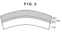
- FIGS. 1 to 3 are sectional views showing the steps in the GaN substrate fabrication method.
- a sapphire underlying substrate 110 is prepared as an underlying substrate.
- a peeling layer (low-temperature GaN buffer layer) 120 is grown on the sapphire underlying substrate 110 at a temperature (low temperature) lower than 1,000°C.
- the peeling layer 120 can be made of, e.g., a single-crystal material, polycrystalline material, or amorphous material of GaN.
- a GaN layer 130 is grown at a temperature (high temperature) of about 1,000°C.
- the GaN layer 130 can be made of, e.g., a single-crystal material of GaN.
- a structure 100 including the peeling layer 120 and GaN layer 130 is formed on the sapphire underlying substrate 110.
- the peeling layer 120 also has a buffering function.
- the sapphire underlying substrate 110 and structure 100 are cooled from about 1,000°C to room temperature.
- the thermal expansion coefficient of the sapphire underlying substrate 110 is higher than that of the GaN layer 130.
- a thermal stress resulting from the thermal expansion coefficient difference acts on the sapphire underlying substrate 110 and GaN layer 130, and warping occurs.
- the peeling layer 120 is melted by the laser lift-off method or the like. This separates the GaN layer 130 from the sapphire underlying substrate 110. That is, a GaN substrate is fabricated by separating the GaN layer 130 from the sapphire underlying substrate 110. In this state, the GaN layer 130 produces a portion in which the internal stress has reduced, and a portion in which the internal stress remains. This may crack the GaN layer 130.
- the separated GaN layer 130 warps because the distribution of strain changes along the crystal growth direction. Accordingly, even when the GaN layer is planarized by a mechanical polishing step, the crystal orientation is distorted as shown in Fig. 3 .
- Patent Reference 1 Japanese Patent Laid-Open No. 2004-39810
- the present invention provides a semiconductor substrate fabrication method capable of increasing the throughput.
- a semiconductor substrate fabrication method is characterized by comprising a preparation step of preparing an underlying substrate, a stacking step of stacking, on the underlying substrate, at least two multilayered films each including a peeling layer and a semiconductor layer, and a separation step of separating the semiconductor layer.
- a semiconductor substrate fabrication method is characterized in that in the separation step, at least two semiconductor layers are separated by selectively etching the peeling layers by using a chemical solution, in addition to having the characteristic of the semiconductor substrate fabrication method according to the first aspect of the present invention.
- a semiconductor substrate fabrication method according to the third aspect of the present invention is characterized in that in the stacking step, stacking is continuously performed without atmospheric exposure, in addition to having the characteristic of the semiconductor substrate fabrication method according to the first or second aspect of the present invention.
- a semiconductor substrate fabrication method according to the fourth aspect of the present invention is characterized in that in the stacking step, stacking is performed in the same apparatus, in addition to having the characteristic of the semiconductor substrate fabrication method according to the first or second aspect of the present invention.
- a semiconductor substrate fabrication method is characterized in that the underlying substrate and the semiconductor layer are made of a single crystal of a compound semiconductor, in addition to having the characteristic of the semiconductor substrate fabrication method according to any one of the first to fourth aspects of the present invention.
- a semiconductor substrate fabrication method is characterized in that the underlying substrate and the semiconductor layer are made of a compound of a group-III element and nitrogen, in addition to having the characteristic of the semiconductor substrate fabrication method according to any one of the first to fifth aspects of the present invention.
- a semiconductor substrate fabrication method is characterized in that the underlying substrate and the semiconductor layer are made of the same material, in addition to having the characteristic of the semiconductor substrate fabrication method according to any one of the first to sixth aspects of the present invention.
- a semiconductor substrate fabrication method is characterized in that the peeling layer comprises at least one of a metal layer and a metal nitride layer, in addition to having the characteristic of the semiconductor substrate fabrication method according to any one of the first to seventh aspects of the present invention.
- a semiconductor substrate fabrication method is characterized in that in the stacking step, the metal nitride layer is formed by nitriding the metal layer in a reaction furnace which grows the semiconductor layer, in addition to having the characteristic of the semiconductor substrate fabrication method according to the eighth aspect of the present invention.
- a semiconductor substrate fabrication method is characterized in that the multilayered film includes a buffer layer between the peeling layer and the semiconductor layer, in addition to having the characteristic of the semiconductor substrate fabrication method according to any one of the first to ninth aspects of the present invention.
- a semiconductor substrate fabrication method according to the 11th aspect of the present invention is characterized in that the buffer layer is made of a single crystal of a compound semiconductor, in addition to having the characteristic of the semiconductor substrate fabrication method according to the 10th aspect of the present invention.
- a semiconductor substrate fabrication method according to the 12th aspect of the present invention is characterized in that the buffer layer is made of a compound of a group-III element and nitrogen, in addition to having the characteristic of the semiconductor substrate fabrication method according to the 10th or 11th aspect of the present invention.
- a semiconductor substrate fabrication method according to the 13th aspect of the present invention is characterized in that the buffer layer and the semiconductor layer are made of the same material, in addition to having the characteristic of the semiconductor substrate fabrication method according to any one of the 10th to 12th aspects of the present invention.
- the present invention can increase the throughput.
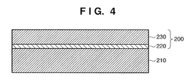
- Figs. 4 to 6 are sectional views of steps showing the problems to be solved by the present invention.
- the present invention is also applicable to a method of fabricating another semiconductor substrate by using another underlying substrate.
- the other underlying substrate can be made of a nitride such as InN, AlN, InGaN, AlGaN, InAlN, or AlInGaIV, a group-IV material such as SiC or Si, an oxide such as Al 2 O 3 , MgAl 2 O 4 , LiGa 2 O 4 , or ZnO, or a nitridable metal such as Fe, Cr, Mo, Ta, Nb, Ti, or Cu.
- the other semiconductor substrate can be made of a nitride such as AlN, InN, or AlGaInN, or an oxide such as ZnO, ZnMgO, ZnCdO, or ZnMgCdO.
- a GaN underlying substrate 210 is prepared as an underlying substrate.
- a peeling layer (metal buffer layer) 220 is formed on the GaN underlying substrate 210.
- the peeling layer 220 can be made of a nitridable metal such as Fe, Cr, Mo, Ta, Nb, Ti, or Cu.
- a GaN layer (semiconductor layer) 230 is grown on the peeling layer 220 at about 1,000°C.
- the GaN layer 230 can be made of, e.g., a single-crystal material of GaN.
- a structure 200 including the peeling layer 220 and GaN layer 230 is formed on the GaN underlying substrate 210.
- the peeling layer 220 also has a buffering function.
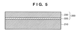
- the GaN underlying substrate 210 and structure 200 are cooled from about 1,000°C to room temperature.
- the thermal expansion coefficient of the GaN underlying substrate 210 is almost equal to that of the GaN layer 230.
- the temperature is lowered from about 1,000°C to room temperature, therefore, almost no thermal stress resulting from the thermal expansion coefficient difference acts on the GaN underlying substrate 210 and GaN layer 230, and almost no warping occurs.
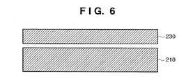
- the peeling layer 220 is selectively etched by using a chemical solution. This separates the GaN layer 230 from the GaN underlying substrate 210. That is, a GaN substrate is fabricated by separating the GaN layer 230 from the GaN underlying substrate 210. In this state, the internal stress is almost uniform in the GaN layer 230. This reduces the possibility of cracking of the GaN layer 230.
- the GaN substrate fabrication method shown in Figs. 4 to 6 generally fabricates only one GaN substrate from the GaN underlying substrate 210. Accordingly, the throughput of the fabrication of GaN substrates is often insufficient.
- FIG. 7 to 11 and 13 to 15 are sectional views showing the steps in the semiconductor substrate fabrication method according to the embodiment of the present invention.
- Fig. 12 is a sectional SEM photograph of a sample obtained by the steps shown in Figs. 7 to 11 .
- the present invention is also applicable to a method of fabricating another semiconductor substrate by using another underlying substrate.
- the other underlying substrate can be made of a nitride such as InN, AlN, InGaN, AlGaN, InAlN, or AlInGaN, a group-IV material such as SiC or Si, an oxide such as Al 2 O 3 , MgAl 2 O 4 , LiGa 2 O 4 , or ZnO, or a nitridable metal such as Fe, Cr, Mo, Ta, Nb, Ti, or Cu.
- the other semiconductor substrate can be made of a nitride such as AlN, InN, or AlGaInN, or an oxide such as ZnO, ZnMgO, ZnCdO, or ZnMgCdO.
- HVPE Hydride Vapor Phase Epitaxy
- MOCVD Metal-Organic Chemical Vapor Deposition
- MOVPE Metal-Organic Vapor Phase Epitaxy
- MBE Molecular Beam Epitaxy
- a GaN underlying substrate 310 is prepared as an underlying substrate.
- the thickness of the GaN underlying substrate 310 is preferably 100 to 500 ⁇ m.
- multilayered film means a film including two or more layers in this specification.
- a peeling layer (metal buffer layer) 320a is deposited on the GaN underlying substrate 310 by sputtering.
- the peeling layer 320a is a nitridable metal layer.
- the peeling layer 320a can be made of a nitridable metal such as Fe, Cr, Mo, Ta, Nb, Ti, or Cu.
- the thickness of the peeling layer 320a is preferably 15 to 75 nm.
- the peeling layer 320a may also be formed by an e-beam evaporator, a thermal evaporator, or the crystal growth method such as CVD, MOCVD, or MBE.
- a portion (upper layer) of the peeling layer 320a is nitrided in an ambience of hydrogen gas containing ammonia at a substrate temperature of 500°C to 1,000°C. Even if a native oxide film exists on the surface of the peeling layer 320a, a strong reducing action of ammonia reduces and nitrides this native oxide film. As a consequence, the peeling layer 320a divides into a first peeling layer 320 and second peeling layer 322.
- the first peeling layer (metal buffer layer) 320 is an unnitrided layer of the peeling layer 320a, and can be made of a nitridable metal such as Fe, Cr, Mo, Ta, Nb, Ti, or Cu.
- the second peeling layer (metal nitride layer) 322 is a nitrided layer of the peeling layer 320a, and can be made of a metal nitride such as Fe 2 N, CrN, MoN, TaN, NbN, TiN, or CuN.
- the first peeling layer 320 is favorably Cr.
- the second peeling layer 322 is favorably CrN.
- the first peeling layer 320 also has a buffering function.
- the second peeling layer 322 also has a buffering function.
- the second peeling layer 322 may also be formed by entirely nitriding the peeling layer 320a.
- the thickness of the second peeling layer 322 is preferably 15 to 75 nm. Depending on the nitrogen conditions, however, the thickness of the second peeling layer 322 is sometimes smaller than that of the peeling layer 320a.
- the flow rate of ammonia, the nitriding temperature, and the nitriding time mainly determine the conditions of the process of forming the uniform second peeling layer 322 on the surface of the peeling layer 320a.
- the process conditions for the purpose are favorably an ammonia flow rate of 1 (1/min), a nitriding temperature of 1,000°C or more, and a nitriding time of 5 min or more.
- the second peeling layer 322 functions as a nucleus for forming GaN layers (a buffer layer 332 and GaN layer 330) in a step shown in Fig. 9 to be described below. Accordingly, the steps shown in Figs. 8 and 9 are preferably successively performed without atmospheric exposure as will be described below.
- the buffer layer 332 is grown on the second peeling layer 322 at a temperature (low temperature) of about 600°C to 1,000°C. More specifically, HCl gas is supplied to a Ga metal material box formed upstream of a reaction chamber via a reaction tube. In the Ga metal material box, the HCl gas and Ga cause a chemical reaction to form GaCl gas. This GaCl gas is supplied from the Ga metal material box to the reaction chamber via the reaction tube. In the reaction chamber, the ammonia-containing hydrogen gas used in the step shown in Fig. 8 remains near the surface of the second peeling layer 322.
- the buffer layer (GaN buffer layer) 332 can be made of, e.g., a single-crystal material, polycrystalline material, or amorphous material of GaN.
- the thickness of the buffer layer 332 is preferably a few ten ⁇ to a few ten ⁇ m.
- the growth temperature of the buffer layer 332 is favorably 800°C to 1,100°C, and more favorably, about 900°C.
- the buffer layer 332 is made of the same material (GaN) as that of the GaN layer (semiconductor layer) 330 to be described later, the GaN layer (semiconductor layer) 330 can easily grow.
- the buffer layer 332 may also be made of a material different from that of the GaN layer (semiconductor layer) 330 to be described later.
- the buffer layer 332 may also be made of a nitride such as AlN, Al x Ga y N, In x Ga y N, or Al x Ga y In z N (wherein 0 ⁇ x ⁇ 1, 0 ⁇ y ⁇ 1, and 0 ⁇ z ⁇ 1), or an oxide such as ZnO.
- the GaN layer (semiconductor layer) 330 is grown on the buffer layer 332 at a temperature (high temperature) of 1,000°C or more.
- the GaN layer (thick GaN layer) 330 can be made of, e.g., a single-crystal material of GaN. Practical conditions are basically the same as those in the step shown in Fig. 9 , except that the flow rate of the HCl gas supplied to the Ga metal material box is high, and the temperature in the reaction chamber is high. Accordingly, the GaN layer 330 grows at a rate (e.g., about 100 ⁇ m/h or more) higher than that in the step shown in Fig. 9 .
- the thickness of the GaN layer 330 is preferably 100 to 500 ⁇ m.
- the growth temperature of the GaN layer 330 is preferably 1,000°C or more.
- the GaN layer 330 may also be controlled to have a conductivity type such as an n-type or p-type by doping a slight amount of an impurity such as Si or Mg during or after the growth.
- the GaN underlying substrate 310 and multilayered film ML1 (in the reaction chamber) are cooled from about 1,000°C to room temperature.
- the thermal expansion coefficient of the GaN underlying substrate 310 is almost equal to that of the GaN layer 330.
- the temperature is lowered from about 1,000°C to room temperature, therefore, almost no thermal stress resulting from the thermal expansion coefficient difference acts on the GaN underlying substrate 310 and GaN layer 330, and almost no warping occurs.
- the multilayered film ML1 as shown in the sectional SEM photograph of Fig. 12 is obtained by steps similar to those shown in Figs. 7 to 11 .
- the GaN underlying substrate 310 and GaN layer 330 have a flat shape. This makes it possible to estimate that almost no warping has occurred in the GaN underlying substrate 310 and GaN layer 330.
- a plurality of multilayered films ML1 to ML3 are formed on the GaN underlying substrate 310 by successively repeating the steps shown in Figs. 7 to 11 without atmospheric exposure. In this way, a structure 300 including the multilayered films ML1 to ML3 is formed on the GaN underlying substrate 310.
- Figs. 7 to 11 can be performed in the same apparatus or in different apparatuses.
- the individual reaction chambers are connected by a mechanism capable of transferring the substrate without exposing it to the atmosphere.
- the first peeling layers 320 and second peeling layers 322 are simultaneously selectively etched by using a chemical solution. That is, as shown in Fig. 14 , the first peeling layers 320 and second peeling layers 322 are etched sideways.
- the etchant (chemical solution) is preferably an aqueous solution mixture of perchloric acid (HClO 4 ) and ammonium cerium secondary nitrate.
- the etchant (chemical solution) is preferably an aqueous nitric acid (HNO 3 ) solution.
- the etching rate of the etchant (chemical solution) can be controlled by the temperature and concentration.
- a plurality of units of the GaN layers 330 and buffer layers 332 are separated from the GaN underlying substrate 310. That is, a plurality of GaN substrates SB1 to SB3 are simultaneously fabricated by separating the units of the GaN layers 330 and buffer layers 332 from the GaN underlying substrate 310. In this state, the internal stress is almost uniform in each GaN layer 330. This reduces the possibility of cracking of each GaN layer 330.
- the buffer layers 332 form portions of the GaN substrates SB1 to SB3 without being etched by the etchant (chemical solution).
- a viscous material may also hold the multilayered films ML1 to ML3 and the GaN underlying substrate 310.
- the GaN substrates SB1 to SB3 may also be simultaneously fabricated by dissolving this viscous material after the first peeling layers 320 and second peeling layers 322 are etched. This makes it possible to stably fabricate the GaN substrates SB1 to SB3.
- the throughput of the fabrication of the GaN substrates SB1 to SB3 can be increased. Also, since the steps shown in Figs. 7 to 11 are successively repeated without atmospheric exposure, it is possible to save the time of evacuation and the time of atmospheric exposure (purging), and further increase the throughput of the fabrication of the GaN substrates. Furthermore, since the GaN substrates SB1 to SB3 are simultaneously fabricated, the fabrication conditions of the GaN substrates SB1 to SB3 can be made uniform, so the variations in quality of the GaN substrates SB1 to SB3 can be reduced.
- steps shown in Figs. 7 to 11 and the steps shown in Figs. 14 and 15 may also be successively performed without atmospheric exposure. In this case, it is possible to save the time of transfer of samples (lots), and further increase the throughput of the fabrication of GaN substrates.
- the number of the multilayered films included in the structure is not limited to three and may also be two or more except three. Increasing the number of the multilayered films included in the structure can further increase the throughput of the fabrication of GaN substrates.
- Three GaN substrates SB1 to SB3 were continuously formed by performing the steps shown in Figs. 7 to 15 (the semiconductor substrate fabrication method according to the embodiment of the present invention) described above.
- the time required from the supply of the samples to the carrying out of the GaN substrates SB1 to SB3 was 26 hrs.
- a first peeling layer 320 and second peeling layer 322 as shown in Fig. 11 were etched, and a unit of a GaN layer 330 and buffer layer 332 was separated from a GaN underlying substrate 310 under the same conditions as shown in Fig. 13 , thereby separately in turn fabricating GaN substrates SB1 to SB3.
- the time required from the supply of the samples to the carrying out of the GaN substrates SB1 to SB3 was 52 hrs.
- the throughput when three semiconductor substrates are continuously formed is about twice that when three semiconductor substrates are separately formed.
Landscapes
- Chemical & Material Sciences (AREA)
- Inorganic Chemistry (AREA)
- Engineering & Computer Science (AREA)
- Crystallography & Structural Chemistry (AREA)
- Materials Engineering (AREA)
- Metallurgy (AREA)
- Organic Chemistry (AREA)
- Crystals, And After-Treatments Of Crystals (AREA)
- Chemical Vapour Deposition (AREA)
Abstract
Description
- The present invention relates to a semiconductor substrate fabrication method.
- A method of fabricating a GaN substrate using a sapphire underlying substrate has been conventionally proposed. The conventional GaN substrate fabrication method will be explained below with reference to
Figs. 1 to 3. Figs. 1 to 3 are sectional views showing the steps in the GaN substrate fabrication method. - In a step shown in
Fig. 1 , a sapphireunderlying substrate 110 is prepared as an underlying substrate. A peeling layer (low-temperature GaN buffer layer) 120 is grown on the sapphire underlyingsubstrate 110 at a temperature (low temperature) lower than 1,000°C. Thepeeling layer 120 can be made of, e.g., a single-crystal material, polycrystalline material, or amorphous material of GaN. Then, a GaNlayer 130 is grown at a temperature (high temperature) of about 1,000°C. The GaNlayer 130 can be made of, e.g., a single-crystal material of GaN. In this manner, astructure 100 including thepeeling layer 120 andGaN layer 130 is formed on the sapphire underlyingsubstrate 110. Note that thepeeling layer 120 also has a buffering function. - In a step shown in
Fig. 2 , the sapphire underlyingsubstrate 110 and structure 100 (in a reaction chamber) are cooled from about 1,000°C to room temperature. The thermal expansion coefficient of the sapphire underlyingsubstrate 110 is higher than that of theGaN layer 130. When the temperature is lowered from about 1,000°C to room temperature, therefore, a thermal stress resulting from the thermal expansion coefficient difference acts on the sapphire underlyingsubstrate 110 andGaN layer 130, and warping occurs. - In a step shown in
Fig. 3 , thepeeling layer 120 is melted by the laser lift-off method or the like. This separates theGaN layer 130 from the sapphire underlyingsubstrate 110. That is, a GaN substrate is fabricated by separating theGaN layer 130 from the sapphire underlyingsubstrate 110. In this state, theGaN layer 130 produces a portion in which the internal stress has reduced, and a portion in which the internal stress remains. This may crack the GaNlayer 130. - The separated
GaN layer 130 warps because the distribution of strain changes along the crystal growth direction. Accordingly, even when the GaN layer is planarized by a mechanical polishing step, the crystal orientation is distorted as shown inFig. 3 . - To reduce this warping, a method of forming a gap between the sapphire underlying
substrate 110 andpeeling layer 120 has been proposed (e.g., patent reference 1).
Patent Reference 1: Japanese Patent Laid-Open No.2004-39810 - In the technique disclosed in patent reference 1, only one semiconductor substrate can be fabricated from the underlying substrate. This decreases the throughput (productivity) in the fabrication of semiconductor substrates.
- The present invention provides a semiconductor substrate fabrication method capable of increasing the throughput.
- A semiconductor substrate fabrication method according to the first aspect of the present invention is characterized by comprising a preparation step of preparing an underlying substrate, a stacking step of stacking, on the underlying substrate, at least two multilayered films each including a peeling layer and a semiconductor layer, and a separation step of separating the semiconductor layer.
- A semiconductor substrate fabrication method according to the second aspect of the present invention is characterized in that in the separation step, at least two semiconductor layers are separated by selectively etching the peeling layers by using a chemical solution, in addition to having the characteristic of the semiconductor substrate fabrication method according to the first aspect of the present invention.
- A semiconductor substrate fabrication method according to the third aspect of the present invention is characterized in that in the stacking step, stacking is continuously performed without atmospheric exposure, in addition to having the characteristic of the semiconductor substrate fabrication method according to the first or second aspect of the present invention.
- A semiconductor substrate fabrication method according to the fourth aspect of the present invention is characterized in that in the stacking step, stacking is performed in the same apparatus, in addition to having the characteristic of the semiconductor substrate fabrication method according to the first or second aspect of the present invention.
- A semiconductor substrate fabrication method according to the fifth aspect of the present invention is characterized in that the underlying substrate and the semiconductor layer are made of a single crystal of a compound semiconductor, in addition to having the characteristic of the semiconductor substrate fabrication method according to any one of the first to fourth aspects of the present invention.
- A semiconductor substrate fabrication method according to the sixth aspect of the present invention is characterized in that the underlying substrate and the semiconductor layer are made of a compound of a group-III element and nitrogen, in addition to having the characteristic of the semiconductor substrate fabrication method according to any one of the first to fifth aspects of the present invention.
- A semiconductor substrate fabrication method according to the seventh aspect of the present invention is characterized in that the underlying substrate and the semiconductor layer are made of the same material, in addition to having the characteristic of the semiconductor substrate fabrication method according to any one of the first to sixth aspects of the present invention.
- A semiconductor substrate fabrication method according to the eighth aspect of the present invention is characterized in that the peeling layer comprises at least one of a metal layer and a metal nitride layer, in addition to having the characteristic of the semiconductor substrate fabrication method according to any one of the first to seventh aspects of the present invention.
- A semiconductor substrate fabrication method according to the ninth aspect of the present invention is characterized in that in the stacking step, the metal nitride layer is formed by nitriding the metal layer in a reaction furnace which grows the semiconductor layer, in addition to having the characteristic of the semiconductor substrate fabrication method according to the eighth aspect of the present invention.
- A semiconductor substrate fabrication method according to the 10th aspect of the present invention is characterized in that the multilayered film includes a buffer layer between the peeling layer and the semiconductor layer, in addition to having the characteristic of the semiconductor substrate fabrication method according to any one of the first to ninth aspects of the present invention.
- A semiconductor substrate fabrication method according to the 11th aspect of the present invention is characterized in that the buffer layer is made of a single crystal of a compound semiconductor, in addition to having the characteristic of the semiconductor substrate fabrication method according to the 10th aspect of the present invention.
- A semiconductor substrate fabrication method according to the 12th aspect of the present invention is characterized in that the buffer layer is made of a compound of a group-III element and nitrogen, in addition to having the characteristic of the semiconductor substrate fabrication method according to the 10th or 11th aspect of the present invention.
- A semiconductor substrate fabrication method according to the 13th aspect of the present invention is characterized in that the buffer layer and the semiconductor layer are made of the same material, in addition to having the characteristic of the semiconductor substrate fabrication method according to any one of the 10th to 12th aspects of the present invention.
- The present invention can increase the throughput.
-
-
Fig. 1 is a sectional view showing a step in a conventional GaN substrate fabrication method; -
Fig. 2 is a sectional view showing another step in the conventional GaN substrate fabrication method; -
Fig. 3 is a sectional view showing still another step in the conventional GaN substrate fabrication method; -
Fig. 4 is a sectional view of a step showing a problem to be solved by the present invention; -
Fig. 5 is a sectional view of another step showing the problem to be solved by the present invention; -
Fig. 6 is a sectional view of still another step showing the problem to be solved by the present invention; -
Fig. 7 is a sectional view showing a step in a semiconductor substrate fabrication method according to an embodiment of the present invention; -
Fig. 8 is a sectional view showing another step in the semiconductor substrate fabrication method according to the embodiment of the present invention; -
Fig. 9 is a sectional view showing still another step in the semiconductor substrate fabrication method according to the embodiment of the present invention; -
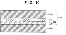
Fig. 10 is a sectional view showing still another step in the semiconductor substrate fabrication method according to the embodiment of the present invention; -
Fig. 11 is a sectional view showing still another step in the semiconductor substrate fabrication method according to the embodiment of the present invention; -
Fig. 12 is a sectional SEM photograph showing a sample obtained by the steps shown inFigs. 7 to 11 ; -
Fig. 13 is a sectional view showing still another step in the semiconductor substrate fabrication method according to the embodiment of the present invention; -
Fig. 14 is a sectional view showing still another step in the semiconductor substrate fabrication method according to the embodiment of the present invention; and -
Fig. 15 is a sectional view showing still another step in the semiconductor substrate fabrication method according to the embodiment of the present invention. - Problems to be solved by the present invention will be explained in detail below with reference to
Figs. 4 to 6. Figs. 4 to 6 are sectional views of steps showing the problems to be solved by the present invention. Although the following explanation will be made by taking a method of fabricating a GaN substrate (semiconductor substrate) by using a GaN underlying substrate (underlying substrate) as an example, the present invention is also applicable to a method of fabricating another semiconductor substrate by using another underlying substrate. The other underlying substrate can be made of a nitride such as InN, AlN, InGaN, AlGaN, InAlN, or AlInGaIV, a group-IV material such as SiC or Si, an oxide such as Al2O3, MgAl2O4, LiGa2O4, or ZnO, or a nitridable metal such as Fe, Cr, Mo, Ta, Nb, Ti, or Cu. The other semiconductor substrate can be made of a nitride such as AlN, InN, or AlGaInN, or an oxide such as ZnO, ZnMgO, ZnCdO, or ZnMgCdO. - In a step shown in
Fig. 4 , a GaN underlyingsubstrate 210 is prepared as an underlying substrate. A peeling layer (metal buffer layer) 220 is formed on the GaN underlyingsubstrate 210. Thepeeling layer 220 can be made of a nitridable metal such as Fe, Cr, Mo, Ta, Nb, Ti, or Cu. - A GaN layer (semiconductor layer) 230 is grown on the
peeling layer 220 at about 1,000°C. TheGaN layer 230 can be made of, e.g., a single-crystal material of GaN. In this manner, astructure 200 including thepeeling layer 220 andGaN layer 230 is formed on the GaNunderlying substrate 210. Note that thepeeling layer 220 also has a buffering function. - In a step shown in
Fig. 5 , the GaNunderlying substrate 210 and structure 200 (in a reaction chamber) are cooled from about 1,000°C to room temperature. The thermal expansion coefficient of the GaNunderlying substrate 210 is almost equal to that of theGaN layer 230. When the temperature is lowered from about 1,000°C to room temperature, therefore, almost no thermal stress resulting from the thermal expansion coefficient difference acts on the GaNunderlying substrate 210 andGaN layer 230, and almost no warping occurs. - In a step shown in
Fig. 6 , thepeeling layer 220 is selectively etched by using a chemical solution. This separates theGaN layer 230 from the GaNunderlying substrate 210. That is, a GaN substrate is fabricated by separating theGaN layer 230 from the GaNunderlying substrate 210. In this state, the internal stress is almost uniform in theGaN layer 230. This reduces the possibility of cracking of theGaN layer 230. - As described above, the GaN substrate fabrication method shown in
Figs. 4 to 6 generally fabricates only one GaN substrate from the GaNunderlying substrate 210. Accordingly, the throughput of the fabrication of GaN substrates is often insufficient. - A semiconductor substrate fabrication method according to an embodiment of the present invention will be explained below with reference to
Figs. 7 to 15 .Figs. 7 to 11 and13 to 15 are sectional views showing the steps in the semiconductor substrate fabrication method according to the embodiment of the present invention.Fig. 12 is a sectional SEM photograph of a sample obtained by the steps shown inFigs. 7 to 11 . Although the following explanation will be made by taking a method of fabricating a GaN substrate (semiconductor substrate) by using a GaN underlying substrate (underlying substrate) as an example, the present invention is also applicable to a method of fabricating another semiconductor substrate by using another underlying substrate. The other underlying substrate can be made of a nitride such as InN, AlN, InGaN, AlGaN, InAlN, or AlInGaN, a group-IV material such as SiC or Si, an oxide such as Al2O3, MgAl2O4, LiGa2O4, or ZnO, or a nitridable metal such as Fe, Cr, Mo, Ta, Nb, Ti, or Cu. The other semiconductor substrate can be made of a nitride such as AlN, InN, or AlGaInN, or an oxide such as ZnO, ZnMgO, ZnCdO, or ZnMgCdO. - In addition, a method using HVPE (Hydride Vapor Phase Epitaxy) will be explained as an example, but the present invention can also be applied to a method using, e.g., MOCVD (Metal-Organic Chemical Vapor Deposition), MOVPE (Metal-Organic Vapor Phase Epitaxy), MBE (Molecular Beam Epitaxy), or the dissolution growth method.
- In a step shown in
Fig. 7 , a GaNunderlying substrate 310 is prepared as an underlying substrate. The thickness of the GaNunderlying substrate 310 is preferably 100 to 500 µm. - Note that a term "multilayered film" means a film including two or more layers in this specification.
- A peeling layer (metal buffer layer) 320a is deposited on the GaN
underlying substrate 310 by sputtering. Thepeeling layer 320a is a nitridable metal layer. Thepeeling layer 320a can be made of a nitridable metal such as Fe, Cr, Mo, Ta, Nb, Ti, or Cu. The thickness of thepeeling layer 320a is preferably 15 to 75 nm. - Note that the
peeling layer 320a may also be formed by an e-beam evaporator, a thermal evaporator, or the crystal growth method such as CVD, MOCVD, or MBE. - In a step shown in
Fig. 8 , a portion (upper layer) of thepeeling layer 320a is nitrided in an ambience of hydrogen gas containing ammonia at a substrate temperature of 500°C to 1,000°C. Even if a native oxide film exists on the surface of thepeeling layer 320a, a strong reducing action of ammonia reduces and nitrides this native oxide film. As a consequence, thepeeling layer 320a divides into afirst peeling layer 320 andsecond peeling layer 322. The first peeling layer (metal buffer layer) 320 is an unnitrided layer of thepeeling layer 320a, and can be made of a nitridable metal such as Fe, Cr, Mo, Ta, Nb, Ti, or Cu. The second peeling layer (metal nitride layer) 322 is a nitrided layer of thepeeling layer 320a, and can be made of a metal nitride such as Fe2N, CrN, MoN, TaN, NbN, TiN, or CuN. Thefirst peeling layer 320 is favorably Cr. Thesecond peeling layer 322 is favorably CrN. - Note that the
first peeling layer 320 also has a buffering function. Similarly, thesecond peeling layer 322 also has a buffering function. Note also that in the step shown inFig. 8 , thesecond peeling layer 322 may also be formed by entirely nitriding thepeeling layer 320a. When thesecond peeling layer 322 is formed by entirely nitriding thepeeling layer 320a, the thickness of thesecond peeling layer 322 is preferably 15 to 75 nm. Depending on the nitrogen conditions, however, the thickness of thesecond peeling layer 322 is sometimes smaller than that of thepeeling layer 320a. - The flow rate of ammonia, the nitriding temperature, and the nitriding time mainly determine the conditions of the process of forming the uniform
second peeling layer 322 on the surface of thepeeling layer 320a. The process conditions for the purpose are favorably an ammonia flow rate of 1 (1/min), a nitriding temperature of 1,000°C or more, and a nitriding time of 5 min or more. - The
second peeling layer 322 functions as a nucleus for forming GaN layers (abuffer layer 332 and GaN layer 330) in a step shown inFig. 9 to be described below. Accordingly, the steps shown inFigs. 8 and9 are preferably successively performed without atmospheric exposure as will be described below. - In the step shown in
Fig. 9 , thebuffer layer 332 is grown on thesecond peeling layer 322 at a temperature (low temperature) of about 600°C to 1,000°C. More specifically, HCl gas is supplied to a Ga metal material box formed upstream of a reaction chamber via a reaction tube. In the Ga metal material box, the HCl gas and Ga cause a chemical reaction to form GaCl gas. This GaCl gas is supplied from the Ga metal material box to the reaction chamber via the reaction tube. In the reaction chamber, the ammonia-containing hydrogen gas used in the step shown inFig. 8 remains near the surface of thesecond peeling layer 322. In the reaction chamber, therefore, the GaCl gas and ammonia gas cause a chemical reaction to form thebuffer layer 332 on thesecond peeling layer 322. The buffer layer (GaN buffer layer) 332 can be made of, e.g., a single-crystal material, polycrystalline material, or amorphous material of GaN. The thickness of thebuffer layer 332 is preferably a few ten Å to a few ten µm. The growth temperature of thebuffer layer 332 is favorably 800°C to 1,100°C, and more favorably, about 900°C. - Since the
buffer layer 332 is made of the same material (GaN) as that of the GaN layer (semiconductor layer) 330 to be described later, the GaN layer (semiconductor layer) 330 can easily grow. - Note that the
buffer layer 332 may also be made of a material different from that of the GaN layer (semiconductor layer) 330 to be described later. For example, thebuffer layer 332 may also be made of a nitride such as AlN, AlxGayN, InxGayN, or AlxGayInzN (wherein 0 < x < 1, 0 < y < 1, and 0 < z < 1), or an oxide such as ZnO. - In a step shown in
Fig. 10 , the GaN layer (semiconductor layer) 330 is grown on thebuffer layer 332 at a temperature (high temperature) of 1,000°C or more. The GaN layer (thick GaN layer) 330 can be made of, e.g., a single-crystal material of GaN. Practical conditions are basically the same as those in the step shown inFig. 9 , except that the flow rate of the HCl gas supplied to the Ga metal material box is high, and the temperature in the reaction chamber is high. Accordingly, theGaN layer 330 grows at a rate (e.g., about 100 µm/h or more) higher than that in the step shown inFig. 9 . The thickness of theGaN layer 330 is preferably 100 to 500 µm. The growth temperature of theGaN layer 330 is preferably 1,000°C or more. As a consequence, a multilayered film ML1 including thefirst peeling layer 320,second peeling layer 322,buffer layer 332, andGaN layer 330 is formed on the GaNunderlying substrate 310. - Note that the
GaN layer 330 may also be controlled to have a conductivity type such as an n-type or p-type by doping a slight amount of an impurity such as Si or Mg during or after the growth. - In the step shown in
Fig. 11 , the GaNunderlying substrate 310 and multilayered film ML1 (in the reaction chamber) are cooled from about 1,000°C to room temperature. The thermal expansion coefficient of the GaNunderlying substrate 310 is almost equal to that of theGaN layer 330. When the temperature is lowered from about 1,000°C to room temperature, therefore, almost no thermal stress resulting from the thermal expansion coefficient difference acts on the GaNunderlying substrate 310 andGaN layer 330, and almost no warping occurs. - For example, the multilayered film ML1 as shown in the sectional SEM photograph of
Fig. 12 is obtained by steps similar to those shown inFigs. 7 to 11 . As shown inFig. 12 , the GaNunderlying substrate 310 andGaN layer 330 have a flat shape. This makes it possible to estimate that almost no warping has occurred in the GaNunderlying substrate 310 andGaN layer 330. - As shown in
Fig. 13 , a plurality of multilayered films ML1 to ML3 are formed on the GaNunderlying substrate 310 by successively repeating the steps shown inFigs. 7 to 11 without atmospheric exposure. In this way, astructure 300 including the multilayered films ML1 to ML3 is formed on the GaNunderlying substrate 310. - The steps shown in
Figs. 7 to 11 can be performed in the same apparatus or in different apparatuses. When these steps are performed in different apparatuses, the individual reaction chambers are connected by a mechanism capable of transferring the substrate without exposing it to the atmosphere. - In steps shown in
Figs. 14 and15 , the first peeling layers 320 and second peeling layers 322 are simultaneously selectively etched by using a chemical solution. That is, as shown inFig. 14 , the first peeling layers 320 and second peeling layers 322 are etched sideways. - When the first peeling layers 320 are made of, e.g., Cr, the etchant (chemical solution) is preferably an aqueous solution mixture of perchloric acid (HClO4) and ammonium cerium secondary nitrate. When the first peeling layers 320 are made of, e.g., Cu, the etchant (chemical solution) is preferably an aqueous nitric acid (HNO3) solution. The etching rate of the etchant (chemical solution) can be controlled by the temperature and concentration.
- When the first peeling layers 320 and second peeling layers 322 are etched, as shown in
Fig. 15 , a plurality of units of the GaN layers 330 andbuffer layers 332 are separated from the GaNunderlying substrate 310. That is, a plurality of GaN substrates SB1 to SB3 are simultaneously fabricated by separating the units of the GaN layers 330 andbuffer layers 332 from the GaNunderlying substrate 310. In this state, the internal stress is almost uniform in eachGaN layer 330. This reduces the possibility of cracking of eachGaN layer 330. - The buffer layers 332 form portions of the GaN substrates SB1 to SB3 without being etched by the etchant (chemical solution).
- Note that in the step shown in
Fig. 13 , a viscous material may also hold the multilayered films ML1 to ML3 and the GaNunderlying substrate 310. In this case, the GaN substrates SB1 to SB3 may also be simultaneously fabricated by dissolving this viscous material after the first peeling layers 320 and second peeling layers 322 are etched. This makes it possible to stably fabricate the GaN substrates SB1 to SB3. - Since the GaN substrates SB1 to SB3 are simultaneously fabricated in the steps shown in
Figs. 14 and15 as described above, the throughput of the fabrication of the GaN substrates SB1 to SB3 can be increased. Also, since the steps shown inFigs. 7 to 11 are successively repeated without atmospheric exposure, it is possible to save the time of evacuation and the time of atmospheric exposure (purging), and further increase the throughput of the fabrication of the GaN substrates. Furthermore, since the GaN substrates SB1 to SB3 are simultaneously fabricated, the fabrication conditions of the GaN substrates SB1 to SB3 can be made uniform, so the variations in quality of the GaN substrates SB1 to SB3 can be reduced. - Note that the steps shown in
Figs. 7 to 11 and the steps shown inFigs. 14 and15 may also be successively performed without atmospheric exposure. In this case, it is possible to save the time of transfer of samples (lots), and further increase the throughput of the fabrication of GaN substrates. - Note also that the number of the multilayered films included in the structure (the
structure 300 shown inFig. 13 ) is not limited to three and may also be two or more except three. Increasing the number of the multilayered films included in the structure can further increase the throughput of the fabrication of GaN substrates. - Three GaN substrates SB1 to SB3 were continuously formed by performing the steps shown in
Figs. 7 to 15 (the semiconductor substrate fabrication method according to the embodiment of the present invention) described above. The time required from the supply of the samples to the carrying out of the GaN substrates SB1 to SB3 was 26 hrs. - On the other hand, after the steps shown in
Figs. 7 to 11 were performed, afirst peeling layer 320 andsecond peeling layer 322 as shown inFig. 11 were etched, and a unit of aGaN layer 330 andbuffer layer 332 was separated from a GaNunderlying substrate 310 under the same conditions as shown inFig. 13 , thereby separately in turn fabricating GaN substrates SB1 to SB3. The time required from the supply of the samples to the carrying out of the GaN substrates SB1 to SB3 was 52 hrs. - As described above, the throughput when three semiconductor substrates are continuously formed is about twice that when three semiconductor substrates are separately formed.
Claims (13)
- A semiconductor substrate fabrication method characterized by comprising:a preparation step of preparing an underlying substrate;a stacking step of stacking, on the underlying substrate, at least two multilayered films each including a peeling layer and a semiconductor layer; anda separation step of separating the semiconductor layer.
- A semiconductor substrate fabrication method according to claim 1, characterized in that,
in the separation step, at least two semiconductor layers are separated by selectively etching the peeling layers by using a chemical solution. - A semiconductor substrate fabrication method according to claim 1 or 2, characterized in that,
in the stacking step, stacking is continuously performed without atmospheric exposure. - A semiconductor substrate fabrication method according to claim 1 or 2, characterized in that,
in the stacking step, stacking is performed in the same apparatus. - A semiconductor substrate fabrication method according to any one of claims 1 to 4, characterized in that
the underlying substrate and the semiconductor layer are made of a single crystal of a compound semiconductor. - A semiconductor substrate fabrication method according to any one of claims 1 to 5, characterized in that
the underlying substrate and the semiconductor layer are made of a compound of a group-III element and nitrogen. - A semiconductor substrate fabrication method according to any one of claims 1 to 6, characterized in that
the underlying substrate and the semiconductor layer are made of the same material. - A semiconductor substrate fabrication method according to any one of claims 1 to 7, characterized in that
the peeling layer comprises at least one of a metal layer and a metal nitride layer. - A semiconductor substrate fabrication method according to claim 8, characterized in that,
in the stacking step, the metal nitride layer is formed by nitriding the metal layer in a reaction furnace which grows the semiconductor layer. - A semiconductor substrate fabrication method according to any one of claims 1 to 9, characterized in
that
the multilayered film includes a buffer layer between the peeling layer and the semiconductor layer. - A semiconductor substrate fabrication method according to claim 10, characterized in that
the buffer layer is made of a single crystal of a compound semiconductor. - A semiconductor substrate fabrication method according to claim 10 or 11, characterized in that
the buffer layer is made of a compound of a group-III element and nitrogen. - A semiconductor substrate fabrication method according to any one of claims 10 to 12, characterized in that
the buffer layer and the semiconductor layer are made of the same material.
Applications Claiming Priority (2)
| Application Number | Priority Date | Filing Date | Title |
|---|---|---|---|
| JP2005244021 | 2005-08-25 | ||
| PCT/JP2006/316635 WO2007023911A1 (en) | 2005-08-25 | 2006-08-24 | Process for producing semiconductor substrate |
Publications (2)
| Publication Number | Publication Date |
|---|---|
| EP1930486A1 true EP1930486A1 (en) | 2008-06-11 |
| EP1930486A4 EP1930486A4 (en) | 2014-01-01 |
Family
ID=37771654
Family Applications (1)
| Application Number | Title | Priority Date | Filing Date |
|---|---|---|---|
| EP06796748.9A Withdrawn EP1930486A4 (en) | 2005-08-25 | 2006-08-24 | PROCESS FOR PRODUCING SEMICONDUCTOR SUBSTRATE |
Country Status (6)
| Country | Link |
|---|---|
| US (1) | US8119499B2 (en) |
| EP (1) | EP1930486A4 (en) |
| JP (1) | JPWO2007023911A1 (en) |
| KR (1) | KR101060289B1 (en) |
| CN (1) | CN101248221B (en) |
| WO (1) | WO2007023911A1 (en) |
Cited By (3)
| Publication number | Priority date | Publication date | Assignee | Title |
|---|---|---|---|---|
| FR2978601A1 (en) * | 2011-07-29 | 2013-02-01 | Nanovation | Method for manufacturing e.g. LED, involves realizing substrate or epitaxial coating containing gallium nitride, and etching sacrificial buffer layer to separate substrate or coating, where substrate is maintained with high temperature |
| CN103748662A (en) * | 2011-06-28 | 2014-04-23 | 圣戈班晶体及检测公司 | Semiconductor substrate and method of forming |
| EP2031642A3 (en) * | 2007-08-28 | 2014-07-02 | DOWA Electronics Materials Co., Ltd. | Group III nitride semiconductor and a manufacturing method thereof |
Families Citing this family (10)
| Publication number | Priority date | Publication date | Assignee | Title |
|---|---|---|---|---|
| JP5076094B2 (en) * | 2007-06-12 | 2012-11-21 | 株式会社 東北テクノアーチ | Group III nitride single crystal manufacturing method, base crystal substrate having metal nitride layer, and multilayer structure wafer |
| JP4877241B2 (en) * | 2008-02-01 | 2012-02-15 | 豊田合成株式会社 | Method for producing group III nitride compound semiconductor substrate |
| WO2010077616A2 (en) * | 2008-12-08 | 2010-07-08 | Alta Devices, Inc. | Multiple stack deposition for epitaxial lift off |
| US8492187B2 (en) * | 2011-09-29 | 2013-07-23 | International Business Machines Corporation | High throughput epitaxial liftoff for releasing multiple semiconductor device layers from a single base substrate |
| KR101505121B1 (en) | 2013-06-21 | 2015-03-23 | 비비에스에이 리미티드 | Method of manufacturing iii-nitride semiconductor layer |
| CN104134608A (en) * | 2014-08-06 | 2014-11-05 | 上海世山科技有限公司 | Method for manufacturing GaN substrate by using chemical etching |
| WO2016100657A2 (en) * | 2014-12-19 | 2016-06-23 | Glo Ab | Method of making a light emitting diode array on a backplane |
| CN109427538B (en) * | 2017-08-24 | 2021-04-02 | 中国科学院上海微系统与信息技术研究所 | A kind of preparation method of heterostructure |
| CN113270358B (en) | 2021-07-15 | 2021-09-14 | 苏州浪潮智能科技有限公司 | A method of making GaN chip and GaN chip |
| KR102897461B1 (en) * | 2022-11-15 | 2025-12-08 | 세종대학교산학협력단 | Compound semiconductor device and method for manufacturing the same |
Family Cites Families (19)
| Publication number | Priority date | Publication date | Assignee | Title |
|---|---|---|---|---|
| JPH088217B2 (en) | 1991-01-31 | 1996-01-29 | 日亜化学工業株式会社 | Crystal growth method for gallium nitride-based compound semiconductor |
| US5290393A (en) | 1991-01-31 | 1994-03-01 | Nichia Kagaku Kogyo K.K. | Crystal growth method for gallium nitride-based compound semiconductor |
| DE69431333T2 (en) * | 1993-10-08 | 2003-07-31 | Mitsubishi Cable Industries, Ltd. | GaN single crystal |
| JP3184717B2 (en) | 1993-10-08 | 2001-07-09 | 三菱電線工業株式会社 | GaN single crystal and method for producing the same |
| US6218207B1 (en) | 1998-05-29 | 2001-04-17 | Mitsushita Electronics Corporation | Method for growing nitride semiconductor crystals, nitride semiconductor device, and method for fabricating the same |
| JP2000049092A (en) * | 1998-05-29 | 2000-02-18 | Matsushita Electron Corp | Crystal growth method of nitride semiconductor, nitride semiconductor device, and method of manufacturing the same |
| TW449937B (en) * | 1999-02-26 | 2001-08-11 | Matsushita Electronics Corp | Semiconductor device and the manufacturing method thereof |
| US6852161B2 (en) * | 2000-08-18 | 2005-02-08 | Showa Denko K.K. | Method of fabricating group-iii nitride semiconductor crystal, method of fabricating gallium nitride-based compound semiconductor, gallium nitride-based compound semiconductor, gallium nitride-based compound semiconductor light-emitting device, and light source using the semiconductor light-emitting device |
| JP4710139B2 (en) * | 2001-01-15 | 2011-06-29 | 豊田合成株式会社 | Group III nitride compound semiconductor device |
| JP3631724B2 (en) * | 2001-03-27 | 2005-03-23 | 日本電気株式会社 | Group III nitride semiconductor substrate and manufacturing method thereof |
| JP2002316898A (en) * | 2001-04-13 | 2002-10-31 | Hitachi Cable Ltd | Method for manufacturing nitride semiconductor substrate and nitride semiconductor substrate |
| JP3812368B2 (en) * | 2001-06-06 | 2006-08-23 | 豊田合成株式会社 | Group III nitride compound semiconductor device and method for manufacturing the same |
| JP4117156B2 (en) * | 2002-07-02 | 2008-07-16 | 日本電気株式会社 | Method for manufacturing group III nitride semiconductor substrate |
| US6818061B2 (en) * | 2003-04-10 | 2004-11-16 | Honeywell International, Inc. | Method for growing single crystal GaN on silicon |
| JP2005001928A (en) | 2003-06-11 | 2005-01-06 | Fujikura Ltd | Self-standing substrate and manufacturing method thereof |
| US7033961B1 (en) * | 2003-07-15 | 2006-04-25 | Rf Micro Devices, Inc. | Epitaxy/substrate release layer |
| JP4218597B2 (en) * | 2003-08-08 | 2009-02-04 | 住友電気工業株式会社 | Manufacturing method of semiconductor light emitting device |
| JP4396816B2 (en) * | 2003-10-17 | 2010-01-13 | 日立電線株式会社 | Group III nitride semiconductor substrate and manufacturing method thereof |
| US7482248B2 (en) * | 2004-12-03 | 2009-01-27 | Semiconductor Energy Laboratory Co., Ltd. | Manufacturing method of semiconductor device |
-
2006
- 2006-08-24 KR KR1020087006102A patent/KR101060289B1/en not_active Expired - Fee Related
- 2006-08-24 EP EP06796748.9A patent/EP1930486A4/en not_active Withdrawn
- 2006-08-24 US US12/064,584 patent/US8119499B2/en active Active
- 2006-08-24 CN CN2006800308730A patent/CN101248221B/en not_active Expired - Fee Related
- 2006-08-24 JP JP2007532177A patent/JPWO2007023911A1/en active Pending
- 2006-08-24 WO PCT/JP2006/316635 patent/WO2007023911A1/en not_active Ceased
Cited By (7)
| Publication number | Priority date | Publication date | Assignee | Title |
|---|---|---|---|---|
| EP2031642A3 (en) * | 2007-08-28 | 2014-07-02 | DOWA Electronics Materials Co., Ltd. | Group III nitride semiconductor and a manufacturing method thereof |
| CN103748662A (en) * | 2011-06-28 | 2014-04-23 | 圣戈班晶体及检测公司 | Semiconductor substrate and method of forming |
| KR20140057249A (en) * | 2011-06-28 | 2014-05-12 | 쌩-고벵 크리스톡스 에 드테끄퇴르 | Semiconductor substrate and method of forming |
| EP2727134A4 (en) * | 2011-06-28 | 2015-04-01 | Saint Gobain Cristaux Et Detecteurs | SEMICONDUCTOR SUBSTRATE AND METHOD OF FORMING THE SAME |
| CN103748662B (en) * | 2011-06-28 | 2016-11-09 | 圣戈班晶体及检测公司 | Semiconductor substrate and forming method |
| KR101983412B1 (en) | 2011-06-28 | 2019-05-28 | 쌩-고벵 크리스톡스 에 드테끄퇴르 | Semiconductor substrate and method of forming |
| FR2978601A1 (en) * | 2011-07-29 | 2013-02-01 | Nanovation | Method for manufacturing e.g. LED, involves realizing substrate or epitaxial coating containing gallium nitride, and etching sacrificial buffer layer to separate substrate or coating, where substrate is maintained with high temperature |
Also Published As
| Publication number | Publication date |
|---|---|
| US20080299746A1 (en) | 2008-12-04 |
| US8119499B2 (en) | 2012-02-21 |
| JPWO2007023911A1 (en) | 2009-03-26 |
| EP1930486A4 (en) | 2014-01-01 |
| WO2007023911A1 (en) | 2007-03-01 |
| KR101060289B1 (en) | 2011-08-29 |
| CN101248221A (en) | 2008-08-20 |
| CN101248221B (en) | 2012-06-06 |
| KR20080043833A (en) | 2008-05-19 |
Similar Documents
| Publication | Publication Date | Title |
|---|---|---|
| US6924159B2 (en) | Semiconductor substrate made of group III nitride, and process for manufacture thereof | |
| EP2064730B1 (en) | Nitride semiconductor structures with interlayer structures and methods of fabricating nitride semiconductor structures with interlayer structures | |
| EP1211715B1 (en) | A method for fabricating a III-V nitride film | |
| EP1997125B1 (en) | Growth method using nanocolumn compliant layers and hvpe for producing high quality compound semiconductor materials | |
| CN102208332B (en) | Thick nitride semiconductor structures with interlayer structures and methods of fabricating thick nitride semiconductor structures | |
| US7674699B2 (en) | III group nitride semiconductor substrate, substrate for group III nitride semiconductor device, and fabrication methods thereof | |
| TWI411711B (en) | Method for forming overlying material on III-N layer and method for growing at least partially covering III-N layer and manufacturing method of unsupported III-N layer and semiconductor device thereof | |
| US9105471B2 (en) | Rare earth oxy-nitride buffered III-N on silicon | |
| GB2485418A (en) | GaN on Si device substrate with GaN layer including sub-10nm SiNx interlayers that promote crystal growth with reduced threading dislocations | |
| WO1999066565A1 (en) | Method and apparatus for producing group-iii nitrides | |
| WO1996041906A1 (en) | Bulk single crystal gallium nitride and method of making same | |
| US20100244100A1 (en) | Compound semiconductor substrate | |
| US8119499B2 (en) | Semiconductor substrate fabrication by etching of a peeling layer | |
| TW200912054A (en) | Method for preparing substrate for growing gallium nitride and method for preparing gallium nitride substrate | |
| US8591652B2 (en) | Semi-conductor substrate and method of masking layer for producing a free-standing semi-conductor substrate by means of hydride-gas phase epitaxy | |
| WO1998024129A1 (en) | Iii-v nitride semiconductor devices and process for the production thereof | |
| CN107227490A (en) | III nitride semiconductor and its manufacture method | |
| US7589345B2 (en) | Nitride-based compound semiconductor substrate and method for fabricating the same | |
| JP2004006568A (en) | Method for manufacturing group 3-5 compound semiconductor | |
| JP2001135575A (en) | Group 3-5 compound semiconductor | |
| WO2015043961A1 (en) | A semiconductor wafer and a method for producing the semiconductor wafer | |
| US6844574B1 (en) | III-V compound semiconductor | |
| JP4507810B2 (en) | Nitride semiconductor substrate manufacturing method and nitride semiconductor substrate | |
| JP2006008500A (en) | Nitride semiconductor substrate manufacturing method and nitride semiconductor substrate | |
| JP2004345868A (en) | Epitaxial substrate and method for reducing dislocation in group iii nitride layer group |
Legal Events
| Date | Code | Title | Description |
|---|---|---|---|
| PUAI | Public reference made under article 153(3) epc to a published international application that has entered the european phase |
Free format text: ORIGINAL CODE: 0009012 |
|
| 17P | Request for examination filed |
Effective date: 20080325 |
|
| AK | Designated contracting states |
Kind code of ref document: A1 Designated state(s): AT BE BG CH CY CZ DE DK EE ES FI FR GB GR HU IE IS IT LI LT LU LV MC NL PL PT RO SE SI SK TR |
|
| RAP1 | Party data changed (applicant data changed or rights of an application transferred) |
Owner name: FURUKAWA CO., LTD. Owner name: EPIVALLEY CO., LTD. Owner name: MITSUBISHI CHEMICAL CORPORATION Owner name: TOHOKU TECHNO ARCH CO., LTD. Owner name: DOWA HOLDINGS CO., LTD Owner name: WAVESQUARE INC. |
|
| RAP1 | Party data changed (applicant data changed or rights of an application transferred) |
Owner name: EPIVALLEY CO., LTD. Owner name: FURUKAWA CO., LTD. Owner name: MITSUBISHI CHEMICAL CORPORATION Owner name: TOHOKU TECHNO ARCH CO., LTD. Owner name: DOWA HOLDINGS CO., LTD Owner name: WAVESQUARE INC. |
|
| DAX | Request for extension of the european patent (deleted) | ||
| A4 | Supplementary search report drawn up and despatched |
Effective date: 20131204 |
|
| RIC1 | Information provided on ipc code assigned before grant |
Ipc: H01L 33/00 20100101ALI20131128BHEP Ipc: H01L 21/02 20060101ALI20131128BHEP Ipc: H01L 21/205 20060101AFI20131128BHEP Ipc: H01L 21/338 20060101ALI20131128BHEP Ipc: H01S 5/323 20060101ALI20131128BHEP Ipc: H01L 21/683 20060101ALI20131128BHEP |
|
| STAA | Information on the status of an ep patent application or granted ep patent |
Free format text: STATUS: THE APPLICATION HAS BEEN WITHDRAWN |
|
| 18W | Application withdrawn |
Effective date: 20150605 |