EP1928088A2 - Acoustic wave device and method of manufacturing the same - Google Patents
Acoustic wave device and method of manufacturing the same Download PDFInfo
- Publication number
- EP1928088A2 EP1928088A2 EP07121369A EP07121369A EP1928088A2 EP 1928088 A2 EP1928088 A2 EP 1928088A2 EP 07121369 A EP07121369 A EP 07121369A EP 07121369 A EP07121369 A EP 07121369A EP 1928088 A2 EP1928088 A2 EP 1928088A2
- Authority
- EP
- European Patent Office
- Prior art keywords
- sealing portion
- acoustic wave
- covered
- forming
- region
- Prior art date
- Legal status (The legal status is an assumption and is not a legal conclusion. Google has not performed a legal analysis and makes no representation as to the accuracy of the status listed.)
- Withdrawn
Links
Images




Classifications
-
- H—ELECTRICITY
- H03—ELECTRONIC CIRCUITRY
- H03H—IMPEDANCE NETWORKS, e.g. RESONANT CIRCUITS; RESONATORS
- H03H3/00—Apparatus or processes specially adapted for the manufacture of impedance networks, resonating circuits, resonators
- H03H3/007—Apparatus or processes specially adapted for the manufacture of impedance networks, resonating circuits, resonators for the manufacture of electromechanical resonators or networks
- H03H3/08—Apparatus or processes specially adapted for the manufacture of impedance networks, resonating circuits, resonators for the manufacture of electromechanical resonators or networks for the manufacture of resonators or networks using surface acoustic waves
-
- H—ELECTRICITY
- H03—ELECTRONIC CIRCUITRY
- H03H—IMPEDANCE NETWORKS, e.g. RESONANT CIRCUITS; RESONATORS
- H03H9/00—Networks comprising electromechanical or electro-acoustic elements; Electromechanical resonators
- H03H9/25—Constructional features of resonators using surface acoustic waves
-
- Y—GENERAL TAGGING OF NEW TECHNOLOGICAL DEVELOPMENTS; GENERAL TAGGING OF CROSS-SECTIONAL TECHNOLOGIES SPANNING OVER SEVERAL SECTIONS OF THE IPC; TECHNICAL SUBJECTS COVERED BY FORMER USPC CROSS-REFERENCE ART COLLECTIONS [XRACs] AND DIGESTS
- Y10—TECHNICAL SUBJECTS COVERED BY FORMER USPC
- Y10T—TECHNICAL SUBJECTS COVERED BY FORMER US CLASSIFICATION
- Y10T29/00—Metal working
- Y10T29/42—Piezoelectric device making
-
- Y—GENERAL TAGGING OF NEW TECHNOLOGICAL DEVELOPMENTS; GENERAL TAGGING OF CROSS-SECTIONAL TECHNOLOGIES SPANNING OVER SEVERAL SECTIONS OF THE IPC; TECHNICAL SUBJECTS COVERED BY FORMER USPC CROSS-REFERENCE ART COLLECTIONS [XRACs] AND DIGESTS
- Y10—TECHNICAL SUBJECTS COVERED BY FORMER USPC
- Y10T—TECHNICAL SUBJECTS COVERED BY FORMER US CLASSIFICATION
- Y10T29/00—Metal working
- Y10T29/49—Method of mechanical manufacture
- Y10T29/49002—Electrical device making
- Y10T29/49005—Acoustic transducer
-
- Y—GENERAL TAGGING OF NEW TECHNOLOGICAL DEVELOPMENTS; GENERAL TAGGING OF CROSS-SECTIONAL TECHNOLOGIES SPANNING OVER SEVERAL SECTIONS OF THE IPC; TECHNICAL SUBJECTS COVERED BY FORMER USPC CROSS-REFERENCE ART COLLECTIONS [XRACs] AND DIGESTS
- Y10—TECHNICAL SUBJECTS COVERED BY FORMER USPC
- Y10T—TECHNICAL SUBJECTS COVERED BY FORMER US CLASSIFICATION
- Y10T29/00—Metal working
- Y10T29/49—Method of mechanical manufacture
- Y10T29/49002—Electrical device making
- Y10T29/49007—Indicating transducer
-
- Y—GENERAL TAGGING OF NEW TECHNOLOGICAL DEVELOPMENTS; GENERAL TAGGING OF CROSS-SECTIONAL TECHNOLOGIES SPANNING OVER SEVERAL SECTIONS OF THE IPC; TECHNICAL SUBJECTS COVERED BY FORMER USPC CROSS-REFERENCE ART COLLECTIONS [XRACs] AND DIGESTS
- Y10—TECHNICAL SUBJECTS COVERED BY FORMER USPC
- Y10T—TECHNICAL SUBJECTS COVERED BY FORMER US CLASSIFICATION
- Y10T29/00—Metal working
- Y10T29/49—Method of mechanical manufacture
- Y10T29/49002—Electrical device making
- Y10T29/4902—Electromagnet, transformer or inductor
- Y10T29/4908—Acoustic transducer
Definitions
- the present invention relates to an acoustic wave device and a method of manufacturing the acoustic wave device, in particular, relates to an acoustic wave device that has a sealing portion having a hollow region above a functional region of an acoustic wave element and a method of manufacturing the acoustic wave device.
- An acoustic wave device is widely used as a signal filter of an electrical and electronic device using an electromagnetic wave.
- the acoustic wave device is used as a transmitting and receiving filter of a radio communication device such as a mobile phone or a frequency filter for visual such as a television or a videotape recorder.
- a chip such as an acoustic wave element is sealed with a sealing portion made of a resin or the like.
- a surface acoustic wave element is one type of an acoustic wave device, and has a structure in which an electrode exciting a surface acoustic wave such as a comb electrode is provided on a piezoelectric substrate made of LiNbO 3 , LiTaO 3 or the like. It is necessary to form a space on the piezoelectric substrate and on the electrode, because the surface acoustic wave propagates on a surface of the piezoelectric substrate. It is necessary to seal the acoustic wave element in order to gain trust, because there is not provided a protective membrane on the piezoelectric substrate and on the electrode.
- Japanese Patent Application Publication No. 9-232900 Japanese Patent Application Publication No. 2002-261582 and Japanese Patent Application Publication No. 2003-37471 disclose an art where a sealing portion is formed on a substrate having an acoustic wave element, and a Wafer Level Package (WLP) is formed, in order to reduce a cost of the acoustic wave device.
- WLP Wafer Level Package
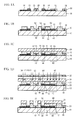
- FIG. 1A through FIG. 2I illustrate a manufacturing method of the acoustic wave device in accordance with the first conventional embodiment.
- FIG. 1A there is formed a comb electrode 12, a wiring 14 connected to the comb electrode 12, a metal pattern 18 in a cutting region 42 (for individuating a wafer) on a substrate 10.
- a protective membrane 20 on the substrate 10, the comb electrode 12 and the wiring 14. A given region of the protective membrane 20 is removed.
- a barrier layer 16 is formed on the wiring 14 in a penetration region 44 (a region where a penetrating electrode is to be formed).
- the first sealing portion 22 is formed so that a functional region 40 (a region where an acoustic wave oscillates), the cutting region 42 and the penetration region 44 (a region where a penetrating electrode is to be formed) act as a first non-covered portion 50, a second non-covered portion 52 and a third non-covered portion 54 (portions not covered with a sealing resin) respectively.
- a photosensitive resin film is adhered onto the first sealing portion 22, and the second sealing portion 24 is formed.
- ultraviolet (UV) ray is radiated to the second sealing portion 24 with use of a mask 32.
- FIG. 1E a region of the second sealing portion 24 to which the ultraviolet (UV) ray is radiated is left after a development. And the second non-covered portion 52, the third non-covered portion 54 and a cavity 60 are formed.
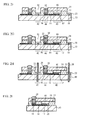
- a penetrating electrode 28 is formed in the third non-covered portion 54.
- a solder ball 30 is formed on the penetrating electrode 28.
- a blade 36 cuts off the substrate 10 along the cutting region 42.
- the acoustic wave device in accordance with the first conventional embodiment is manufactured.
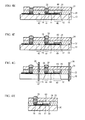
- FIG. 3A through FIG. 4H illustrate a method of manufacturing the acoustic wave device in accordance with the second conventional embodiment.
- the first sealing portion 22 is formed so that the functional region 40 and the penetration region 44 act as the first non-covered portion 50 and the third non-covered portion 54 respectively.
- the first sealing portion 22 is left in the cutting region 42, being different from the first conventional embodiment shown in FIG. 1B .
- a photosensitive film is adhered onto the first sealing portion 22, and the second sealing portion 24 is formed.
- an ultraviolet (UV) ray is radiated to the second sealing portion 24 with use of the mask 32.
- a region of the second sealing portion 24 to which the ultraviolet (UV) ray is radiated is left after a development.
- the third non-covered portion 54 and the cavity 60 are formed.
- the second sealing portion 24 is left in the cutting region 42, being different from the first conventional embodiment shown in FIG. 1E .
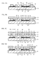
- the penetrating electrode 28 is formed in the third non-covered portion 54.
- the solder ball 30 is formed on the penetrating electrode 28.
- the blade 36 cuts off the substrate 10, the first sealing portion 22 and the second sealing portion 24 along the cutting region 42.
- the acoustic wave device in accordance with the second conventional embodiment is thus manufactured.
- the first sealing portion 22 has a hollow region above the functional region 40, and the second sealing portion 24 covers the hollow region.
- the acoustic wave element is sealed.
- the solder ball 30 is connected to the acoustic wave element via the penetrating electrode 28.
- the acoustic wave element is flip-chip mounted with the solder ball 30.
- an electrical signal of the acoustic wave element is output to outside.
- a cutting load is small when a wafer is cut into a chip, because the first sealing portion 22 and the second sealing portion 24 in the cutting region 42 are removed as shown in FIG. 2H .
- a foreign particle is adhered to the cutting region 42 in a process between sealing the substrate 10 shown in FIG. 1E and cutting the substrate shown in FIG. 2H , if the sealing portion is not provided on the cutting region 42.
- a metal used for the penetrating electrode 28 in FIG. 2F and a solder used for the solder ball 30 in FIG. 2G drop into the second non-covered portion 52 in the cutting region 42.
- the chip size may be enlarged if an interval is enlarged between the cutting region 42 and the penetrating electrode 28 in order to solve the problem.
- a metal, a solder or the like does not drop into the cutting region 42 when the penetrating electrode 28 and the solder ball 30 are formed as shown in FIG. 4E and FIG. 4F , in a case where the first sealing portion 22 and the second sealing portion 24 are left in the cutting region 42 as shown in FIG. 3A through FIG. 4E .
- the wafer is warped because of a contraction pressure of the first sealing portion 22 and the second sealing portion 24 in a heating process of hardening the first sealing portion 22 and the second sealing portion 24 or in a reflow process of the solder.
- the present invention has been made in view of the above circumstances and may restrain an adherence of a foreign particle to a cutting region and a warp of a wafer in process of manufacture.
- a method of manufacturing an acoustic wave device including forming a first sealing portion on a substrate having an acoustic wave element thereon so that a functional region, in which an acoustic wave oscillates, of the acoustic wave element acts as a first non-covered portion and a cutting region for individuating acts as a second non-covered portion, forming a second sealing portion on the first sealing portion so as to cover the first non-covered portion and the second non-covered portion, and cutting off the substrate and the second sealing portion so that the second non-covered portion is divided.
- the method it may be possible to restrain an adherence of a foreign particle to the cutting region in the manufacturing process, because the second sealing portion covers the cutting region in the manufacturing process. And it may be possible to restrain a warp of a wafer because the second non-covered portion in the cutting region reduces a stress.
- a method of manufacturing an acoustic wave device including forming a first sealing portion on a substrate having an acoustic wave element thereon so that a functional region, in which an acoustic wave oscillates, of the acoustic wave element acts as a first non-covered portion, forming a second sealing portion on the first sealing portion so that the second sealing portion covers the first non-covered portion and a region on the first sealing portion in a cutting region for individuating acts as a second non-covered portion, forming a third sealing portion on the second sealing portion so as to cover the second non-covered portion, and cutting the substrate, the first sealing portion and the third sealing portion so that the second non-covered portion is divided.
- the method it may be possible to restrain an adherence of a foreign particle to the cutting region in the manufacturing process, because the third sealing portion covers the cutting region in the manufacturing process. And it may be possible to restrain a warp of a wafer because the second non-covered portion in the cutting region reduces a stress.
- an acoustic wave device including a substrate having an acoustic wave element thereon, a first sealing portion that is provided on the substrate so that a functional region, in which an acoustic wave oscillates, of the acoustic wave element acts as a first non-covered portion, and a second sealing portion that is provided on the first sealing portion so that the first non-covered portion has a hollow shape.
- a side face of the first sealing portion is inside of a side face of the substrate and the second sealing portion.
- the structure it may be possible to restrain an adherence of a foreign particle to a cutting region in a manufacturing process of the acoustic wave device, because the second sealing portion covers the cutting region in the manufacturing process. And it may be possible to restrain a warp of a wafer because a non-covered portion in the cutting region reduces a stress.
- an acoustic wave device including a substrate having an acoustic wave element thereon, a first sealing portion that is provided on the substrate so that a functional region, in which an acoustic wave oscillates, of the acoustic wave element acts as a first non-covered portion, a second sealing portion that is provided on the first sealing portion so that the first non-covered portion has a hollow shape, and a third sealing portion provided on the second sealing portion.
- a side face of the second sealing portion is inside of a side face of the substrate, the first sealing portion and the third sealing portion.
- the structure it may be possible to restrain an adherence of a foreign particle to a cutting region in a manufacturing process of the acoustic wave device, because the third sealing portion covers the cutting region in the manufacturing process. And it may be possible to restrain a warp of a wafer because a non-covered portion in the cutting region reduces a stress.
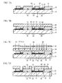
- FIG. 5A through FIG. 6H illustrate a cross sectional view showing a manufacturing process of an acoustic wave device in accordance with a first embodiment.
- the comb electrode 12 As shown in FIG. 5A , there are formed the comb electrode 12, the wiring 14 connected to the comb electrode 12, and the metal pattern 18 in the cutting region 42 on the piezoelectric substrate 10 made of LiTaO 3 (lithium tantalate), with Al (aluminum)-Cu (copper).
- the comb electrode 12 is an electrode exciting a surface acoustic wave of the piezoelectric substrate 10, and forms the acoustic wave element.
- the protective membrane 20 made of SiO 2 (silicon oxide) membrane is formed on the substrate 10, the comb electrode 12 and the wiring 14. A given region of the protective membrane 20 is removed.
- the barrier layer 16 made of Ti (titanium) / Au (gold) is formed on the wiring 14 in the penetration region 44 where a penetrating electrode is to be formed.
- a permanent negative resist made of an epoxy is spin-coated on the substrate 10 by 30 ⁇ m.
- the first sealing portion 22 in the functional region 40, in the cutting region 42 and in the penetration region 44 is removed after an exposure and a development.
- the first non-covered portion 50, the second non-covered portion 52 and the third non-covered portion 54 are formed.
- the first sealing portion 22 is formed so that the functional region 40 acts as the first non-covered portion 50, the cutting region 42 acts as the second non-covered portion 52, and the penetration region 44 acts as the third non-covered portion 54.
- the epoxy permanent negative resist having a thickness of 30 ⁇ m and acting as the second sealing portion 24 is adhered onto the first sealing portion 22 with a tenting method.
- an ultra violet ray 34 is radiated to the second sealing portion 24 with use of the mask 32.
- the third non-covered portion 54 in the first sealing portion 22 and in the second sealing portion 24 is formed in the penetration region 44, and the cavity 60 and a cavity 62 covered with the second sealing portion 24 are formed on the functional region 40 and on the cutting region 42.
- a post bake is performed for an hour at a temperature of 250 degrees C in order to thermally harden the second sealing portion 24. The post bake causes a warp of a 4 inches wafer by approximately 200 ⁇ m.
- Ni nickel having a thickness of approximately 50 ⁇ m is formed in the third non-covered portion 54 with an electroplating.
- a surface of the Ni is subjected to a flash plating ofAu (gold), and the penetrating electrode 28 made of the Ni is formed.
- SnAgCu titanium copper solder paste is mask-printed and reflowed on the penetrating electrode 28, and the solder ball 30 is formed.
- the wafer warps by approximately 200 ⁇ m after the reflow process in which the solder ball 30 is formed. The warp of the wafer after the reflow is substantially the same as that before the reflow.
- the blade 36 cuts off the second sealing portion 24 and the substrate 10 along the cutting region 42 with a dicing method. In this case, a peeling of the first sealing portion 22 and the second sealing portion 24 is not observed.
- the acoustic wave device shown in FIG. 6H is manufactured. As shown in FIG. 6H , in the acoustic wave device, a side face T1 of the first sealing portion 22 is inside of a side face T2 of the substrate 10 and the second sealing portion 24.
- the cutting region 42 has a width of approximately 100 ⁇ m. And a distance W1 between the side face T1 and the side face T2 is approximately 5 ⁇ m to 10 ⁇ m.
- the first sealing portion 22 is formed so that the functional region 40 acts as the first non-covered portion 50 and the cutting region 42 acts as the second non-covered portion 52 on the substrate 10 where the acoustic wave element is formed, as shown in FIG. 5A .
- the second sealing portion 24 is formed on the first sealing portion 22 so as to cover the first non-covered portion 50 and the second non-covered portion 52 and form the cavity 60.
- the substrate 10 and the second sealing portion 24 are cut off so that the second non-covered portion 52 is divided.
- the cutting region 42 is covered with the second sealing portion 24 when the penetrating electrode 28 and the solder ball 30 are being formed, as shown in FIG.
- the first sealing portion 22 and the second sealing portion 24 are formed so that the penetration region 44 acts as the third non-covered portion 54, in the process of forming the first sealing portion 22 and in the process of forming the second sealing portion 24.
- the penetrating electrode 28 is formed in the third non-covered portion 54 and is electrically connected to the acoustic wave element. It is therefore possible to form the penetrating electrode 28 that passes through the first sealing portion 22 and the second sealing portion 24 and is electrically connected to the acoustic wave element via the wiring 14. It is possible to obtain an electrical signal from an upper face of the second sealing portion 24. And it is possible to restrain the adherence of a foreign particle to the cutting region 42 when the penetrating electrode 28 is formed.
- FIG. 7A through FIG. 9J illustrate a cross sectional view showing a manufacturing method of an acoustic wave device in accordance with a second embodiment.
- the first sealing portion 22 having a thickness of approximately 30 ⁇ m is formed on the substrate 10.
- the second non-covered portion is not formed in the cutting region 42, being different from the first embodiment shown in FIG. 5A .
- the first sealing portion 22 is left.
- the other process is the same as that of the first embodiment shown in FIG. 5A .
- the second sealing portion 24 having a thickness of approximately 30 ⁇ m is formed on the first sealing portion 22.
- an ultra violet ray UV ray
- the second non-covered portion 52 and the third non-covered portion 54 are formed in the second sealing portion 24.
- the second non-covered portion 52 is formed in the cutting region 42, being different from the first embodiment shown in FIG. 5D .
- the other process is the same as the first embodiment shown in FIG. 5D .
- the epoxy permanent negative resist having a thickness of 30 ⁇ m and acting as a third sealing portion 26 is adhered onto the second sealing portion 24 with a tenting method.
- the third non-covered portion 54 in the first sealing portion 22, in the second sealing portion 24 and in the third sealing portion 26 are formed in the penetration region 44 after an exposure and a development.
- the cutting region 42 is covered with the third sealing portion 26.
- the cavity 62 is formed.
- the penetrating electrode 28 is formed in the third non-covered portion 54, as is the case of the first embodiment shown in FIG. 6E .
- the solder ball is formed on the penetrating electrode 28, as is the case of the first embodiment shown in FIG 6F .
- the blade 36 cuts off the third sealing portion 26, the first sealing portion 22 and the substrate 10 along the cutting region 42 with the dicing method, as is the case of the first embodiment shown in FIG 6G In this case, a peeling of the first sealing portion 22 and the second sealing portion 24 is not observed.
- the side face T1 of the second sealing portion 24 is inside of the side face T2 of the substrate 10, the first sealing portion 22 and the second sealing portion 24.
- the first sealing portion 22 is formed so that the functional region 40 acts as the first non-covered portion 50, as shown in FIG 7A .
- the second sealing portion 24 is formed on the first sealing portion 22 so that the second sealing portion 24 covers the first non-covered portion 50, a cavity is formed in the first non-covered portion 50, and a region of the cutting region 42 above the first sealing portion 22 acts as the second non-covered portion 52.
- the third sealing portion 26 is formed on the second sealing portion 24 so as to cover the second non-covered portion 52.
- the substrate 10, the first sealing portion 22 and the third sealing portion 26 are cut off so that the second non-covered portion 52 is divided.
- the cutting region 42 is covered with the third sealing portion 26 when the penetrating electrode 28 and the solder ball 30 are being formed, as shown in FIG. 9G and FIG 9H. It is therefore possible to restrain the adherence of a foreign particle to the cutting region 42 as shown in the first embodiment. It is possible to reduce the warp of the wafer, because a contraction pressure of the first sealing portion 22, the second sealing portion 24, and the third sealing portion 26 generated in the post bake shown in FIG 7D and FIG 8F or in the solder reflow process shown in FIG 8H is reduced because of the cavity 62 in the cutting region 42.
- the third sealing portion 26 is formed so that the penetration region 44 where the penetrating electrode is to be formed acts as the third non-covered portion 54, in addition to the process of forming the first sealing portion 22 and the second sealing portion 24 in accordance with the first embodiment.
- the penetrating electrode 28 is formed in the third non-covered portion 54 and is electrically connected to the acoustic wave element. It is therefore possible to form the penetrating electrode 28 that passes through the first sealing portion 22 through the third sealing portion 26 and is electrically connected to the acoustic wave element via the wiring 14. It is possible to obtain an electrical signal from an upper face of the third sealing portion 26. And it is possible to restrain the adherence of a foreign particle to the cutting region 42 when the penetrating electrode 28 is formed.
- the photosensitive resin is formed when the first sealing portion 22 is formed, as shown in FIG. 5B and FIG. 7B .
- the first non-covered portion 50 is formed with the exposure shown in FIG. 5C and FIG. 7C . With the processes, it is possible to easily form the first non-covered portion 50 in the first sealing portion 22.
- FIG. 6E and FIG. 8G show the process of forming the Ni in the third non-covered portion 54 with the electroplating as a process of forming the penetrating electrode 28.
- the penetrating electrode 28 may be an electrically conductive material including at least one of Ag (silver), Cu (copper), SnAg (tin silver) and SnAgCu (tin silver copper).
- the penetrating electrode 28 may be formed with a method other than the electroplating, for example a printing process.
- the solder ball 30 may be made of a solder such as a SnAg (tin silver) solder or a SnAgCu (tin silver copper) solder.
- the acoustic wave element has the substrate 10 made of LiTaO 3 (lithium tantalate).
- the acoustic wave element may have a piezoelectric substrate such as LiNbO 3 (lithium niobate) substrate.
- the acoustic wave element is not limited to the surface acoustic wave element.
- a FBAR Fin bulk acoustic resonator
- the acoustic wave element may be the FBAR.
Landscapes
- Physics & Mathematics (AREA)
- Acoustics & Sound (AREA)
- Engineering & Computer Science (AREA)
- Manufacturing & Machinery (AREA)
- Surface Acoustic Wave Elements And Circuit Networks Thereof (AREA)
- Encapsulation Of And Coatings For Semiconductor Or Solid State Devices (AREA)
Abstract
Description
- The present invention relates to an acoustic wave device and a method of manufacturing the acoustic wave device, in particular, relates to an acoustic wave device that has a sealing portion having a hollow region above a functional region of an acoustic wave element and a method of manufacturing the acoustic wave device.
- An acoustic wave device is widely used as a signal filter of an electrical and electronic device using an electromagnetic wave. The acoustic wave device is used as a transmitting and receiving filter of a radio communication device such as a mobile phone or a frequency filter for visual such as a television or a videotape recorder. In the acoustic wave device, a chip such as an acoustic wave element is sealed with a sealing portion made of a resin or the like. A surface acoustic wave element is one type of an acoustic wave device, and has a structure in which an electrode exciting a surface acoustic wave such as a comb electrode is provided on a piezoelectric substrate made of LiNbO3, LiTaO3 or the like. It is necessary to form a space on the piezoelectric substrate and on the electrode, because the surface acoustic wave propagates on a surface of the piezoelectric substrate. It is necessary to seal the acoustic wave element in order to gain trust, because there is not provided a protective membrane on the piezoelectric substrate and on the electrode.
-
Japanese Patent Application Publication No. 9-232900 Japanese Patent Application Publication No. 2002-261582 Japanese Patent Application Publication No. 2003-37471 - A description will be given of a method of manufacturing an acoustic wave device in accordance with a first conventional embodiment that does not have a
first sealing portion 22 and asecond sealing portion 24 in a cutting region.FIG. 1A through FIG. 2I illustrate a manufacturing method of the acoustic wave device in accordance with the first conventional embodiment. As shown inFIG. 1A , there is formed acomb electrode 12, awiring 14 connected to thecomb electrode 12, ametal pattern 18 in a cutting region 42 (for individuating a wafer) on asubstrate 10. There is formed aprotective membrane 20 on thesubstrate 10, thecomb electrode 12 and thewiring 14. A given region of theprotective membrane 20 is removed. Abarrier layer 16 is formed on thewiring 14 in a penetration region 44 (a region where a penetrating electrode is to be formed). As shown inFIG. 1B , thefirst sealing portion 22 is formed so that a functional region 40 (a region where an acoustic wave oscillates), thecutting region 42 and the penetration region 44 (a region where a penetrating electrode is to be formed) act as a first non-coveredportion 50, a second non-coveredportion 52 and a third non-covered portion 54 (portions not covered with a sealing resin) respectively. - As shown in
FIG. 1C , a photosensitive resin film is adhered onto thefirst sealing portion 22, and thesecond sealing portion 24 is formed. As shown inFIG 1D , ultraviolet (UV) ray is radiated to thesecond sealing portion 24 with use of amask 32. As shown inFIG. 1E , a region of thesecond sealing portion 24 to which the ultraviolet (UV) ray is radiated is left after a development. And the second non-coveredportion 52, the third non-coveredportion 54 and acavity 60 are formed. - As shown in
FIG. 2F , a penetratingelectrode 28 is formed in the third non-coveredportion 54. As shown inFIG. 2G , asolder ball 30 is formed on the penetratingelectrode 28. As shown inFIG. 2H , ablade 36 cuts off thesubstrate 10 along thecutting region 42. As shown inFIG. 2I , the acoustic wave device in accordance with the first conventional embodiment is manufactured. - Next, a description will be given of a method of manufacturing an acoustic wave device in accordance with a second conventional embodiment in which the
first sealing portion 22 and thesecond sealing portion 24 are formed in thecutting region 42.FIG. 3A through FIG. 4H illustrate a method of manufacturing the acoustic wave device in accordance with the second conventional embodiment. As shown inFIG. 3A , thefirst sealing portion 22 is formed so that thefunctional region 40 and thepenetration region 44 act as the first non-coveredportion 50 and the third non-coveredportion 54 respectively. Thefirst sealing portion 22 is left in thecutting region 42, being different from the first conventional embodiment shown inFIG. 1B . - As shown in
FIG. 3B , a photosensitive film is adhered onto thefirst sealing portion 22, and thesecond sealing portion 24 is formed. As shown inFIG. 3C , an ultraviolet (UV) ray is radiated to thesecond sealing portion 24 with use of themask 32. As shown inFIG. 3D , a region of thesecond sealing portion 24 to which the ultraviolet (UV) ray is radiated is left after a development. And the thirdnon-covered portion 54 and thecavity 60 are formed. Thesecond sealing portion 24 is left in thecutting region 42, being different from the first conventional embodiment shown inFIG. 1E . - As shown in
FIG. 4E , thepenetrating electrode 28 is formed in the third non-coveredportion 54. As shown inFIG. 4F , thesolder ball 30 is formed on the penetratingelectrode 28. As shown inFIG. 4G , theblade 36 cuts off thesubstrate 10, thefirst sealing portion 22 and thesecond sealing portion 24 along thecutting region 42. As shown inFIG. 4H , the acoustic wave device in accordance with the second conventional embodiment is thus manufactured. - In accordance with the first conventional embodiment and the second conventional embodiment, the
first sealing portion 22 has a hollow region above thefunctional region 40, and thesecond sealing portion 24 covers the hollow region. Thus, the acoustic wave element is sealed. Thesolder ball 30 is connected to the acoustic wave element via thepenetrating electrode 28. The acoustic wave element is flip-chip mounted with thesolder ball 30. Thus, an electrical signal of the acoustic wave element is output to outside. - In the first conventional embodiment, a cutting load is small when a wafer is cut into a chip, because the
first sealing portion 22 and thesecond sealing portion 24 in the cuttingregion 42 are removed as shown inFIG. 2H . However, there is a case where a foreign particle is adhered to the cuttingregion 42 in a process between sealing thesubstrate 10 shown inFIG. 1E and cutting the substrate shown inFIG. 2H , if the sealing portion is not provided on the cuttingregion 42. For example, a metal used for the penetratingelectrode 28 inFIG. 2F and a solder used for thesolder ball 30 inFIG. 2G drop into the secondnon-covered portion 52 in the cuttingregion 42. The chip size may be enlarged if an interval is enlarged between the cuttingregion 42 and the penetratingelectrode 28 in order to solve the problem. - On the other hand, in the second conventional embodiment, a metal, a solder or the like does not drop into the cutting
region 42 when the penetratingelectrode 28 and thesolder ball 30 are formed as shown inFIG. 4E and FIG. 4F , in a case where thefirst sealing portion 22 and thesecond sealing portion 24 are left in the cuttingregion 42 as shown inFIG. 3A through FIG. 4E . However, the wafer is warped because of a contraction pressure of thefirst sealing portion 22 and thesecond sealing portion 24 in a heating process of hardening thefirst sealing portion 22 and thesecond sealing portion 24 or in a reflow process of the solder. - The present invention has been made in view of the above circumstances and may restrain an adherence of a foreign particle to a cutting region and a warp of a wafer in process of manufacture.
- According to an embodiment of an aspect of the present invention, there is provided a method of manufacturing an acoustic wave device including forming a first sealing portion on a substrate having an acoustic wave element thereon so that a functional region, in which an acoustic wave oscillates, of the acoustic wave element acts as a first non-covered portion and a cutting region for individuating acts as a second non-covered portion, forming a second sealing portion on the first sealing portion so as to cover the first non-covered portion and the second non-covered portion, and cutting off the substrate and the second sealing portion so that the second non-covered portion is divided.
- With the method, it may be possible to restrain an adherence of a foreign particle to the cutting region in the manufacturing process, because the second sealing portion covers the cutting region in the manufacturing process. And it may be possible to restrain a warp of a wafer because the second non-covered portion in the cutting region reduces a stress.
- According to an embodiment of another aspect of the present invention, there is provided a method of manufacturing an acoustic wave device including forming a first sealing portion on a substrate having an acoustic wave element thereon so that a functional region, in which an acoustic wave oscillates, of the acoustic wave element acts as a first non-covered portion, forming a second sealing portion on the first sealing portion so that the second sealing portion covers the first non-covered portion and a region on the first sealing portion in a cutting region for individuating acts as a second non-covered portion, forming a third sealing portion on the second sealing portion so as to cover the second non-covered portion, and cutting the substrate, the first sealing portion and the third sealing portion so that the second non-covered portion is divided.
- With the method, it may be possible to restrain an adherence of a foreign particle to the cutting region in the manufacturing process, because the third sealing portion covers the cutting region in the manufacturing process. And it may be possible to restrain a warp of a wafer because the second non-covered portion in the cutting region reduces a stress.
- According to an embodiment of another aspect of the present invention, there is provided an acoustic wave device including a substrate having an acoustic wave element thereon, a first sealing portion that is provided on the substrate so that a functional region, in which an acoustic wave oscillates, of the acoustic wave element acts as a first non-covered portion, and a second sealing portion that is provided on the first sealing portion so that the first non-covered portion has a hollow shape. A side face of the first sealing portion is inside of a side face of the substrate and the second sealing portion.
- With the structure, it may be possible to restrain an adherence of a foreign particle to a cutting region in a manufacturing process of the acoustic wave device, because the second sealing portion covers the cutting region in the manufacturing process. And it may be possible to restrain a warp of a wafer because a non-covered portion in the cutting region reduces a stress.
- According to an embodiment of another aspect of the present invention, there is provided an acoustic wave device including a substrate having an acoustic wave element thereon, a first sealing portion that is provided on the substrate so that a functional region, in which an acoustic wave oscillates, of the acoustic wave element acts as a first non-covered portion, a second sealing portion that is provided on the first sealing portion so that the first non-covered portion has a hollow shape, and a third sealing portion provided on the second sealing portion. A side face of the second sealing portion is inside of a side face of the substrate, the first sealing portion and the third sealing portion.
- With the structure, it may be possible to restrain an adherence of a foreign particle to a cutting region in a manufacturing process of the acoustic wave device, because the third sealing portion covers the cutting region in the manufacturing process. And it may be possible to restrain a warp of a wafer because a non-covered portion in the cutting region reduces a stress.
- Preferred embodiments of the present invention will be described in detail with reference to the following drawings, wherein:
-
FIG. 1A through FIG. 1E illustrate a manufacturing process of an acoustic wave device in accordance with a first previously-considered arrangement; -
FIG. 2F through FIG. 2I illustrate the manufacturing process of the acoustic wave device in accordance with the first previously-considered arrangement; -
FIG. 3A through FIG. 3D illustrate a manufacturing process of an acoustic wave device in accordance with a second previously-considered arrangement; -
FIG. 4E through FIG. 4H illustrate the manufacturing process of the acoustic wave device in accordance with the second previously-considered arrangement; -
FIG. 5A through FIG. 5D illustrate a manufacturing process of an acoustic wave device in accordance with a first embodiment; -
FIG. 6E through FIG. 6H illustrate the manufacturing process of the acoustic wave device in accordance with the first embodiment; -
FIG. 7A through FIG. 7D illustrate a manufacturing process of an acoustic wave device in accordance with a second embodiment; -
FIG 8E through FIG 8H illustrate the manufacturing process of the acoustic wave device in accordance with the second embodiment; and -
FIG 9I and FIG 9J illustrate the manufacturing process of the acoustic wave device in accordance with the second embodiment. - A description will now be given, with reference to the accompanying drawings, of embodiments of the present invention.
-
FIG. 5A through FIG. 6H illustrate a cross sectional view showing a manufacturing process of an acoustic wave device in accordance with a first embodiment. As shown inFIG. 5A , there are formed thecomb electrode 12, thewiring 14 connected to thecomb electrode 12, and themetal pattern 18 in the cuttingregion 42 on thepiezoelectric substrate 10 made of LiTaO3 (lithium tantalate), with Al (aluminum)-Cu (copper). Thecomb electrode 12 is an electrode exciting a surface acoustic wave of thepiezoelectric substrate 10, and forms the acoustic wave element. Theprotective membrane 20 made of SiO2 (silicon oxide) membrane is formed on thesubstrate 10, thecomb electrode 12 and thewiring 14. A given region of theprotective membrane 20 is removed. Thebarrier layer 16 made of Ti (titanium) / Au (gold) is formed on thewiring 14 in thepenetration region 44 where a penetrating electrode is to be formed. A permanent negative resist made of an epoxy is spin-coated on thesubstrate 10 by 30 µm. Thefirst sealing portion 22 in thefunctional region 40, in the cuttingregion 42 and in thepenetration region 44 is removed after an exposure and a development. Thus, the firstnon-covered portion 50, the secondnon-covered portion 52 and the thirdnon-covered portion 54 are formed. Thefirst sealing portion 22 is formed so that thefunctional region 40 acts as the firstnon-covered portion 50, the cuttingregion 42 acts as the secondnon-covered portion 52, and thepenetration region 44 acts as the thirdnon-covered portion 54. - As shown in
FIG. 5B , the epoxy permanent negative resist having a thickness of 30 µm and acting as thesecond sealing portion 24 is adhered onto thefirst sealing portion 22 with a tenting method. As shown inFIG. 5C , anultra violet ray 34 is radiated to thesecond sealing portion 24 with use of themask 32. As shown inFIG. 5D , the thirdnon-covered portion 54 in thefirst sealing portion 22 and in thesecond sealing portion 24 is formed in thepenetration region 44, and thecavity 60 and acavity 62 covered with thesecond sealing portion 24 are formed on thefunctional region 40 and on the cuttingregion 42. A post bake is performed for an hour at a temperature of 250 degrees C in order to thermally harden thesecond sealing portion 24. The post bake causes a warp of a 4 inches wafer by approximately 200 µm. - As shown in
FIG. 6E , Ni (nickel) having a thickness of approximately 50 µm is formed in the thirdnon-covered portion 54 with an electroplating. A surface of the Ni is subjected to a flash plating ofAu (gold), and the penetratingelectrode 28 made of the Ni is formed. As shown inFIG. 6F , SnAgCu (tin silver copper) solder paste is mask-printed and reflowed on the penetratingelectrode 28, and thesolder ball 30 is formed. The wafer warps by approximately 200 µm after the reflow process in which thesolder ball 30 is formed. The warp of the wafer after the reflow is substantially the same as that before the reflow. - As shown in
FIG. 6G , theblade 36 cuts off thesecond sealing portion 24 and thesubstrate 10 along the cuttingregion 42 with a dicing method. In this case, a peeling of thefirst sealing portion 22 and thesecond sealing portion 24 is not observed. With the processes, the acoustic wave device shown inFIG. 6H is manufactured. As shown inFIG. 6H , in the acoustic wave device, a side face T1 of thefirst sealing portion 22 is inside of a side face T2 of thesubstrate 10 and thesecond sealing portion 24. In the first embodiment, the cuttingregion 42 has a width of approximately 100 µm. And a distance W1 between the side face T1 and the side face T2 is approximately 5 µm to 10 µm. - In the manufacturing method in accordance with the first embodiment, the
first sealing portion 22 is formed so that thefunctional region 40 acts as the firstnon-covered portion 50 and the cuttingregion 42 acts as the secondnon-covered portion 52 on thesubstrate 10 where the acoustic wave element is formed, as shown inFIG. 5A . As shown inFIG. 5D , thesecond sealing portion 24 is formed on thefirst sealing portion 22 so as to cover the firstnon-covered portion 50 and the secondnon-covered portion 52 and form thecavity 60. As shown inFIG. 6G , thesubstrate 10 and thesecond sealing portion 24 are cut off so that the secondnon-covered portion 52 is divided. With the processes, the cuttingregion 42 is covered with thesecond sealing portion 24 when the penetratingelectrode 28 and thesolder ball 30 are being formed, as shown inFIG. 6E and FIG. 6F . It is therefore possible to restrain the adherence of a foreign particle to the cuttingregion 42 as shown in the first conventional embodiment. It is possible to reduce the warp of the wafer, because a contraction pressure of thefirst sealing portion 22 and thesecond sealing portion 24 generated in the post bake shown inFIG. 5D or in the solder reflow process shown inFIG 6F is reduced because of thecavity 62 in the cuttingregion 42. - As shown in
FIG. 5A through FIG. 5G , thefirst sealing portion 22 and thesecond sealing portion 24 are formed so that thepenetration region 44 acts as the thirdnon-covered portion 54, in the process of forming thefirst sealing portion 22 and in the process of forming thesecond sealing portion 24. And, as shown inFIG. 6E , the penetratingelectrode 28 is formed in the thirdnon-covered portion 54 and is electrically connected to the acoustic wave element. It is therefore possible to form the penetratingelectrode 28 that passes through thefirst sealing portion 22 and thesecond sealing portion 24 and is electrically connected to the acoustic wave element via thewiring 14. It is possible to obtain an electrical signal from an upper face of thesecond sealing portion 24. And it is possible to restrain the adherence of a foreign particle to the cuttingregion 42 when the penetratingelectrode 28 is formed. -
FIG. 7A through FIG. 9J illustrate a cross sectional view showing a manufacturing method of an acoustic wave device in accordance with a second embodiment. As shown inFIG. 7A , thefirst sealing portion 22 having a thickness of approximately 30 µm is formed on thesubstrate 10. The second non-covered portion is not formed in the cuttingregion 42, being different from the first embodiment shown inFIG. 5A . And thefirst sealing portion 22 is left. The other process is the same as that of the first embodiment shown inFIG. 5A . - As shown in
FIG. 7B , thesecond sealing portion 24 having a thickness of approximately 30 µm is formed on thefirst sealing portion 22. As shown inFIG. 7C , an ultra violet ray (UV ray) is radiated to thesecond sealing portion 24 with use of themask 32. As shown inFIG. 7D , the secondnon-covered portion 52 and the thirdnon-covered portion 54 are formed in thesecond sealing portion 24. The secondnon-covered portion 52 is formed in the cuttingregion 42, being different from the first embodiment shown inFIG. 5D . The other process is the same as the first embodiment shown inFIG. 5D . - As shown in
FIG. 8E , the epoxy permanent negative resist having a thickness of 30 µm and acting as athird sealing portion 26 is adhered onto thesecond sealing portion 24 with a tenting method. As shown inFIG. 8F , the thirdnon-covered portion 54 in thefirst sealing portion 22, in thesecond sealing portion 24 and in thethird sealing portion 26 are formed in thepenetration region 44 after an exposure and a development. The cuttingregion 42 is covered with thethird sealing portion 26. And thecavity 62 is formed. - As shown in
FIG. 8G , the penetratingelectrode 28 is formed in the thirdnon-covered portion 54, as is the case of the first embodiment shown inFIG. 6E . As shown inFIG 8H , the solder ball is formed on the penetratingelectrode 28, as is the case of the first embodiment shown inFIG 6F . - As shown in
FIG. 9I , theblade 36 cuts off thethird sealing portion 26, thefirst sealing portion 22 and thesubstrate 10 along the cuttingregion 42 with the dicing method, as is the case of the first embodiment shown inFIG 6G In this case, a peeling of thefirst sealing portion 22 and thesecond sealing portion 24 is not observed. As shown inFIG 9J , in the acoustic wave device, the side face T1 of thesecond sealing portion 24 is inside of the side face T2 of thesubstrate 10, thefirst sealing portion 22 and thesecond sealing portion 24. - In the manufacturing method in accordance with the second embodiment, the
first sealing portion 22 is formed so that thefunctional region 40 acts as the firstnon-covered portion 50, as shown inFIG 7A . As shown inFIG 7D , thesecond sealing portion 24 is formed on thefirst sealing portion 22 so that thesecond sealing portion 24 covers the firstnon-covered portion 50, a cavity is formed in the firstnon-covered portion 50, and a region of the cuttingregion 42 above thefirst sealing portion 22 acts as the secondnon-covered portion 52. As shown inFIG 8F , thethird sealing portion 26 is formed on thesecond sealing portion 24 so as to cover the secondnon-covered portion 52. As shown inFIG 9I , thesubstrate 10, thefirst sealing portion 22 and thethird sealing portion 26 are cut off so that the secondnon-covered portion 52 is divided. With the processes, the cuttingregion 42 is covered with thethird sealing portion 26 when the penetratingelectrode 28 and thesolder ball 30 are being formed, as shown in FIG. 9G and FIG 9H. It is therefore possible to restrain the adherence of a foreign particle to the cuttingregion 42 as shown in the first embodiment. It is possible to reduce the warp of the wafer, because a contraction pressure of thefirst sealing portion 22, thesecond sealing portion 24, and thethird sealing portion 26 generated in the post bake shown inFIG 7D andFIG 8F or in the solder reflow process shown inFIG 8H is reduced because of thecavity 62 in the cuttingregion 42. - As shown in
FIG 8F , in the second embodiment, thethird sealing portion 26 is formed so that thepenetration region 44 where the penetrating electrode is to be formed acts as the thirdnon-covered portion 54, in addition to the process of forming thefirst sealing portion 22 and thesecond sealing portion 24 in accordance with the first embodiment. And as shown inFIG 8G , the penetratingelectrode 28 is formed in the thirdnon-covered portion 54 and is electrically connected to the acoustic wave element. It is therefore possible to form the penetratingelectrode 28 that passes through thefirst sealing portion 22 through thethird sealing portion 26 and is electrically connected to the acoustic wave element via thewiring 14. It is possible to obtain an electrical signal from an upper face of thethird sealing portion 26. And it is possible to restrain the adherence of a foreign particle to the cuttingregion 42 when the penetratingelectrode 28 is formed. - In the first embodiment and the second embodiment, the photosensitive resin is formed when the
first sealing portion 22 is formed, as shown inFIG. 5B andFIG. 7B . The firstnon-covered portion 50 is formed with the exposure shown inFIG. 5C andFIG. 7C . With the processes, it is possible to easily form the firstnon-covered portion 50 in thefirst sealing portion 22. - It is possible to form the photosensitive resin by coating the epoxy negative resist as shown in
FIG. 5B andFIG. 7B . It is therefore possible to easily form the photosensitive resist acting as thefirst sealing portion 22. - It is possible to form a film-shaped photosensitive resin sheet on the
first sealing portion 22 as shown inFIG. 5B andFIG. 7B , when thesecond sealing portion 24 is formed. It is therefore possible to cover the firstnon-covered portion 50 with thesecond sealing portion 24 with a resin not being adhered to the inside of the firstnon-covered portion 50. And it is possible to form thecavity 60. -
FIG. 6E andFIG. 8G show the process of forming the Ni in the thirdnon-covered portion 54 with the electroplating as a process of forming the penetratingelectrode 28. The penetratingelectrode 28 may be an electrically conductive material including at least one of Ag (silver), Cu (copper), SnAg (tin silver) and SnAgCu (tin silver copper). The penetratingelectrode 28 may be formed with a method other than the electroplating, for example a printing process. - In accordance with the first embodiment and the second embodiment, it is possible to restrain the adherence of a foreign particle to the cutting
region 42 when thesolder call 30 is formed on the penetratingelectrode 28 as shown inFIG. 6F andFIG. 8H . Thesolder ball 30 may be made of a solder such as a SnAg (tin silver) solder or a SnAgCu (tin silver copper) solder. - In the first embodiment and the second embodiment, the acoustic wave element has the
substrate 10 made of LiTaO3 (lithium tantalate). The acoustic wave element may have a piezoelectric substrate such as LiNbO3 (lithium niobate) substrate. The acoustic wave element is not limited to the surface acoustic wave element. For example, it is necessary that a FBAR (Film bulk acoustic resonator) should have a cavity above a functional region where an acoustic wave oscillates. Therefore, the acoustic wave element may be the FBAR. - While the above description constitutes the preferred embodiments of the present invention, it will be appreciated that the invention is susceptible of modification, variation and change without departing from the proper scope and fair meaning of the accompanying claims.
- The present application is based on
Japanese Patent Application No. 2006-320891 filed on November 28, 2006
Claims (16)
- A method of manufacturing an acoustic wave device comprising:forming a first sealing portion on a substrate having an acoustic wave element thereon so that a functional region, in which an acoustic wave oscillates, of the acoustic wave element acts as a first non-covered portion and a cutting region for individuating acts as a second non-covered portion;forming a second sealing portion on the first sealing portion so as to cover the first non-covered portion and the second non-covered portion; andcutting off the substrate and the second sealing portion so that the second non-covered portion is divided.
- The method as claimed in claim 1, wherein:the step of forming the first sealing portion is a step of forming the first sealing portion so that a given region where a penetrating electrode is to be formed acts as a third non-covered portion;the step of forming the second sealing portion is a step of forming the second sealing portion so that the region where the penetrating electrode is to be formed acts as the third non-covered portion; andthe method further includes forming the penetrating electrode in the third non-covered portion.
- A method of manufacturing an acoustic wave device comprising:forming a first sealing portion on a substrate having an acoustic wave element thereon so that a functional region, in which an acoustic wave oscillates, of the acoustic wave element acts as a first non-covered portion;forming a second sealing portion on the first sealing portion so that the second sealing portion covers the first non-covered portion and a region on the first sealing portion in a cutting region for individuating acts as a second non-covered portion;forming a third sealing portion on the second sealing portion so as to cover the second non-covered portion; andcutting the substrate, the first sealing portion and the third sealing portion so that the second non-covered portion is divided.
- The method as claimed in claim 3, wherein:the step of forming the first sealing portion is a step of forming the first sealing portion so that a region where a penetrating electrode is to be formed acts as a third non-covered portion;the step of forming the second sealing portion is a step of forming the second sealing portion so that the region where the penetrating electrode is to be formed acts as the third non-covered portion;the step of forming the third sealing portion is a step of forming the third sealing portion so that the region where the penetrating electrode is to be formed acts as the third non-covered portion; andthe method further includes forming the penetrating electrode in the third non-covered portion.
- The method as claimed in claim 2 or 4, wherein the step of forming the penetrating electrode includes forming the penetrating electrode in the third non-covered portion with an electroplating method.
- The method as claimed in claim 2, 4 or 5, further comprising forming a solder ball on the penetrating electrode.
- The method as claimed in any preceding claim, wherein the step of forming the first sealing portion includes forming a photosensitive resin, and forming the first non-covered portion by exposing the photosensitive resin.
- The method as claimed in claim 7, wherein the step of forming the first photosensitive resin includes coating an epoxy negative resist.
- The method as claimed in any preceding claim, wherein the step of forming the second sealing portion includes forming a film-shaped photosensitive resin sheet on the first sealing portion.
- An acoustic wave device comprising:a substrate having an acoustic wave element thereon;a first sealing portion that is provided on the substrate so that a functional region, in which an acoustic wave oscillates, of the acoustic wave element acts as a first non-covered portion; anda second sealing portion that is provided on the first sealing portion so that the first non-covered portion has a hollow shape,wherein a side face of the first sealing portion is inside of a side face of the substrate and the second sealing portion.
- The acoustic wave device as claimed in claim 10 further comprising a penetrating electrode that passes through the first sealing portion and the second sealing portion and is connected to the acoustic wave element.
- An acoustic wave device comprising:a substrate having an acoustic wave element thereon;a first sealing portion that is provided on the substrate so that a functional region, in which an acoustic wave oscillates, of the acoustic wave element acts as a first non-covered portion;a second sealing portion that is provided on the first sealing portion so that the first non-covered portion has a hollow shape; anda third sealing portion provided on the second sealing portion,wherein a side face of the second sealing portion is inside of a side face of the substrate, the first sealing portion and the third sealing portion.
- The acoustic wave device as claimed in claim 12 further comprising a penetrating electrode that passes through the first sealing portion, the second sealing portion and the third sealing portion and is connected to the acoustic wave element.
- The acoustic wave device as claimed in claim 11 or 13, further comprising a solder ball on the penetrating electrode.
- The acoustic wave device as claimed in any of claims 10 to 14, wherein the first sealing portion and the second sealing portion are made of a resin.
- The acoustic wave device as claimed in any of claims 10 to 15, wherein the penetrating electrode includes a conductive material including at least one of Ag, Cu, Ni, SnAg and SnAgCu.
Applications Claiming Priority (1)
| Application Number | Priority Date | Filing Date | Title |
|---|---|---|---|
| JP2006320891A JP4886485B2 (en) | 2006-11-28 | 2006-11-28 | Elastic wave device and manufacturing method thereof |
Publications (2)
| Publication Number | Publication Date |
|---|---|
| EP1928088A2 true EP1928088A2 (en) | 2008-06-04 |
| EP1928088A3 EP1928088A3 (en) | 2008-08-06 |
Family
ID=39146652
Family Applications (1)
| Application Number | Title | Priority Date | Filing Date |
|---|---|---|---|
| EP07121369A Withdrawn EP1928088A3 (en) | 2006-11-28 | 2007-11-22 | Acoustic wave device and method of manufacturing the same |
Country Status (5)
| Country | Link |
|---|---|
| US (1) | US7841064B2 (en) |
| EP (1) | EP1928088A3 (en) |
| JP (1) | JP4886485B2 (en) |
| KR (1) | KR100891418B1 (en) |
| CN (1) | CN101192815B (en) |
Families Citing this family (7)
| Publication number | Priority date | Publication date | Assignee | Title |
|---|---|---|---|---|
| WO2009057699A1 (en) * | 2007-10-30 | 2009-05-07 | Kyocera Corporation | Elastic wave device |
| KR101166637B1 (en) * | 2007-12-14 | 2012-07-18 | 가부시키가이샤 무라타 세이사쿠쇼 | Surface wave device and method of manufacturing the same |
| JP5588836B2 (en) * | 2010-11-12 | 2014-09-10 | 太陽誘電株式会社 | Elastic wave device |
| JP5141852B2 (en) | 2011-03-28 | 2013-02-13 | 株式会社村田製作所 | Electronic component and manufacturing method thereof |
| JP5873311B2 (en) | 2011-11-29 | 2016-03-01 | 太陽誘電株式会社 | Elastic wave device and multilayer substrate |
| JP6261867B2 (en) | 2013-01-25 | 2018-01-17 | 太陽誘電株式会社 | Method for manufacturing acoustic wave device |
| JP6646089B2 (en) * | 2018-02-22 | 2020-02-14 | 京セラ株式会社 | Elastic wave device and circuit board |
Family Cites Families (13)
| Publication number | Priority date | Publication date | Assignee | Title |
|---|---|---|---|---|
| JP3634055B2 (en) | 1996-02-26 | 2005-03-30 | 株式会社日立国際電気 | Surface acoustic wave device and manufacturing method thereof |
| JP2000114918A (en) * | 1998-10-05 | 2000-04-21 | Mitsubishi Electric Corp | Surface acoustic wave device and method of manufacturing the same |
| JP2001053178A (en) * | 1999-06-02 | 2001-02-23 | Japan Radio Co Ltd | Electronic component in which electronic circuit device is sealed and mounted on circuit board, and method of manufacturing the same |
| DE10006446A1 (en) * | 2000-02-14 | 2001-08-23 | Epcos Ag | Encapsulation for an electrical component and method of manufacture |
| US6703768B2 (en) * | 2000-09-27 | 2004-03-09 | Citizen Watch Co., Ltd. | Piezoelectric generator and mounting structure therefor |
| JP2002261582A (en) | 2000-10-04 | 2002-09-13 | Matsushita Electric Ind Co Ltd | Surface acoustic wave device, method of manufacturing the same, and circuit module using the same |
| JP3772702B2 (en) | 2001-07-23 | 2006-05-10 | 松下電器産業株式会社 | Manufacturing method of surface acoustic wave device |
| KR100431181B1 (en) * | 2001-12-07 | 2004-05-12 | 삼성전기주식회사 | Method of packaging surface acoustic wave device |
| JP4179038B2 (en) * | 2002-06-03 | 2008-11-12 | 株式会社村田製作所 | Surface acoustic wave device |
| KR100541084B1 (en) * | 2003-08-20 | 2006-01-11 | 삼성전기주식회사 | Method for manufacturing surface acoustic wave filter package and package sheet used therein |
| KR100680511B1 (en) * | 2004-07-14 | 2007-02-08 | 가부시키가이샤 무라타 세이사쿠쇼 | Piezoelectric devices |
| JP2006217225A (en) | 2005-02-03 | 2006-08-17 | Matsushita Electric Ind Co Ltd | Manufacturing method of surface acoustic wave device |
| KR100691160B1 (en) * | 2005-05-06 | 2007-03-09 | 삼성전기주식회사 | Laminated surface acoustic wave package and manufacturing method thereof |
-
2006
- 2006-11-28 JP JP2006320891A patent/JP4886485B2/en not_active Expired - Fee Related
-
2007
- 2007-11-22 EP EP07121369A patent/EP1928088A3/en not_active Withdrawn
- 2007-11-27 KR KR1020070121710A patent/KR100891418B1/en not_active Expired - Fee Related
- 2007-11-27 CN CN2007101946294A patent/CN101192815B/en not_active Expired - Fee Related
- 2007-11-28 US US11/987,173 patent/US7841064B2/en not_active Expired - Fee Related
Also Published As
| Publication number | Publication date |
|---|---|
| US20080125662A1 (en) | 2008-05-29 |
| JP2008135998A (en) | 2008-06-12 |
| CN101192815B (en) | 2010-04-07 |
| KR100891418B1 (en) | 2009-04-02 |
| US7841064B2 (en) | 2010-11-30 |
| KR20080048421A (en) | 2008-06-02 |
| EP1928088A3 (en) | 2008-08-06 |
| JP4886485B2 (en) | 2012-02-29 |
| CN101192815A (en) | 2008-06-04 |
Similar Documents
| Publication | Publication Date | Title |
|---|---|---|
| US7259500B2 (en) | Piezoelectric device | |
| US7586240B2 (en) | Acoustic wave device | |
| JP4460612B2 (en) | Surface acoustic wave device and manufacturing method thereof | |
| US8004160B2 (en) | Acoustic wave device with adhesive layer and method of manufacturing the same | |
| KR100642932B1 (en) | Piezoelectric parts | |
| US7259032B2 (en) | Hermetically sealing a package to include a barrier metal | |
| EP2256924B1 (en) | Piezoelectric component and manufacturing method thereof | |
| US20100045145A1 (en) | Piezoelectric component and manufacturing method thereof | |
| US7841064B2 (en) | Method of manufacturing an acoustic wave device | |
| EP1526640A1 (en) | Piezoelectric component and method for manufacturing the same | |
| JP2018098816A (en) | Elastic wave device and elastic wave module | |
| EP2267895B1 (en) | Electronic component, circuit board, electronic apparatus, and method for manufacturing the electronic component | |
| US7721411B2 (en) | Method of manufacturing an acoustic wave device | |
| US20080122314A1 (en) | Acoustic wave device | |
| US7102272B2 (en) | Piezoelectric component and method for manufacturing the same | |
| JP2005217670A (en) | Surface acoustic wave device and communication device | |
| JP2001077658A (en) | Surface acoustic wave device | |
| JP2003158436A (en) | Manufacturing method of surface acoustic wave device | |
| KR20060118062A (en) | Surface acoustic wave filter package and substrate manufacturing method thereof and substrate for surface acoustic wave filter package manufactured by the same | |
| JP2004328336A (en) | Surface acoustic wave filter | |
| JP2009278654A (en) | Resonator | |
| JP2005223432A (en) | Surface acoustic wave device and manufacturing method thereof |
Legal Events
| Date | Code | Title | Description |
|---|---|---|---|
| PUAI | Public reference made under article 153(3) epc to a published international application that has entered the european phase |
Free format text: ORIGINAL CODE: 0009012 |
|
| AK | Designated contracting states |
Kind code of ref document: A2 Designated state(s): AT BE BG CH CY CZ DE DK EE ES FI FR GB GR HU IE IS IT LI LT LU LV MC MT NL PL PT RO SE SI SK TR |
|
| AX | Request for extension of the european patent |
Extension state: AL BA HR MK RS |
|
| PUAL | Search report despatched |
Free format text: ORIGINAL CODE: 0009013 |
|
| AK | Designated contracting states |
Kind code of ref document: A3 Designated state(s): AT BE BG CH CY CZ DE DK EE ES FI FR GB GR HU IE IS IT LI LT LU LV MC MT NL PL PT RO SE SI SK TR |
|
| AX | Request for extension of the european patent |
Extension state: AL BA HR MK RS |
|
| 17P | Request for examination filed |
Effective date: 20090128 |
|
| AKX | Designation fees paid |
Designated state(s): DE FR GB |
|
| RAP1 | Party data changed (applicant data changed or rights of an application transferred) |
Owner name: TAIYO YUDEN CO., LTD. Owner name: FUJITSU MEDIA DEVICES LIMITED |
|
| RAP1 | Party data changed (applicant data changed or rights of an application transferred) |
Owner name: TAIYO YUDEN CO., LTD. |
|
| STAA | Information on the status of an ep patent application or granted ep patent |
Free format text: STATUS: THE APPLICATION HAS BEEN WITHDRAWN |
|
| 18W | Application withdrawn |
Effective date: 20111108 |