EP1926355B1 - Method for manufacturing an extendable circuit support and extendable circuit support - Google Patents
Method for manufacturing an extendable circuit support and extendable circuit support Download PDFInfo
- Publication number
- EP1926355B1 EP1926355B1 EP07076013.7A EP07076013A EP1926355B1 EP 1926355 B1 EP1926355 B1 EP 1926355B1 EP 07076013 A EP07076013 A EP 07076013A EP 1926355 B1 EP1926355 B1 EP 1926355B1
- Authority
- EP
- European Patent Office
- Prior art keywords
- extensible
- electronic component
- foil
- conductor structure
- substrate layer
- Prior art date
- Legal status (The legal status is an assumption and is not a legal conclusion. Google has not performed a legal analysis and makes no representation as to the accuracy of the status listed.)
- Active
Links
- 238000000034 method Methods 0.000 title claims description 50
- 238000004519 manufacturing process Methods 0.000 title claims description 10
- 239000000758 substrate Substances 0.000 claims description 82
- 239000004020 conductor Substances 0.000 claims description 75
- 239000007858 starting material Substances 0.000 claims description 35
- 239000000463 material Substances 0.000 claims description 30
- 239000011888 foil Substances 0.000 claims description 19
- RYGMFSIKBFXOCR-UHFFFAOYSA-N Copper Chemical compound [Cu] RYGMFSIKBFXOCR-UHFFFAOYSA-N 0.000 claims description 6
- 230000002787 reinforcement Effects 0.000 claims description 5
- 238000005266 casting Methods 0.000 claims description 4
- 229920001971 elastomer Polymers 0.000 claims description 4
- 229910052802 copper Inorganic materials 0.000 claims description 3
- 239000010949 copper Substances 0.000 claims description 3
- PCHJSUWPFVWCPO-UHFFFAOYSA-N gold Chemical compound [Au] PCHJSUWPFVWCPO-UHFFFAOYSA-N 0.000 claims description 3
- 229910052737 gold Inorganic materials 0.000 claims description 3
- 239000010931 gold Substances 0.000 claims description 3
- 229920000126 latex Polymers 0.000 claims description 3
- 239000004816 latex Substances 0.000 claims description 3
- 229920001296 polysiloxane Polymers 0.000 claims description 3
- 238000007639 printing Methods 0.000 claims description 3
- 229910052709 silver Inorganic materials 0.000 claims description 3
- 239000004332 silver Substances 0.000 claims description 3
- 238000010030 laminating Methods 0.000 claims description 2
- 229920002635 polyurethane Polymers 0.000 claims description 2
- 239000004814 polyurethane Substances 0.000 claims description 2
- 238000000151 deposition Methods 0.000 claims 4
- 230000008021 deposition Effects 0.000 claims 2
- BQCADISMDOOEFD-UHFFFAOYSA-N Silver Chemical compound [Ag] BQCADISMDOOEFD-UHFFFAOYSA-N 0.000 claims 1
- 238000000465 moulding Methods 0.000 claims 1
- 239000000969 carrier Substances 0.000 description 6
- 238000003475 lamination Methods 0.000 description 5
- 239000004433 Thermoplastic polyurethane Substances 0.000 description 4
- 239000000853 adhesive Substances 0.000 description 4
- 230000001070 adhesive effect Effects 0.000 description 4
- 238000000059 patterning Methods 0.000 description 4
- 230000003014 reinforcing effect Effects 0.000 description 4
- 238000005476 soldering Methods 0.000 description 4
- 229920002803 thermoplastic polyurethane Polymers 0.000 description 4
- 239000011889 copper foil Substances 0.000 description 3
- 238000005516 engineering process Methods 0.000 description 3
- 238000002844 melting Methods 0.000 description 3
- 230000008018 melting Effects 0.000 description 3
- 238000000206 photolithography Methods 0.000 description 3
- 229920001169 thermoplastic Polymers 0.000 description 3
- 239000004416 thermosoftening plastic Substances 0.000 description 3
- 238000003466 welding Methods 0.000 description 3
- 238000004026 adhesive bonding Methods 0.000 description 2
- 238000011161 development Methods 0.000 description 2
- 230000018109 developmental process Effects 0.000 description 2
- 238000009792 diffusion process Methods 0.000 description 2
- 239000000835 fiber Substances 0.000 description 2
- 239000002184 metal Substances 0.000 description 2
- 229910052751 metal Inorganic materials 0.000 description 2
- 239000002245 particle Substances 0.000 description 2
- 239000004033 plastic Substances 0.000 description 2
- 229920003023 plastic Polymers 0.000 description 2
- 239000002861 polymer material Substances 0.000 description 2
- 239000000843 powder Substances 0.000 description 2
- 230000005855 radiation Effects 0.000 description 2
- 230000002040 relaxant effect Effects 0.000 description 2
- 238000007650 screen-printing Methods 0.000 description 2
- 230000001960 triggered effect Effects 0.000 description 2
- 241001136792 Alle Species 0.000 description 1
- 230000005540 biological transmission Effects 0.000 description 1
- 150000001875 compounds Chemical class 0.000 description 1
- 238000001816 cooling Methods 0.000 description 1
- 238000004132 cross linking Methods 0.000 description 1
- 230000001419 dependent effect Effects 0.000 description 1
- 238000013461 design Methods 0.000 description 1
- 239000012777 electrically insulating material Substances 0.000 description 1
- 230000010354 integration Effects 0.000 description 1
- 239000000203 mixture Substances 0.000 description 1
- 229920000642 polymer Polymers 0.000 description 1
- 238000012545 processing Methods 0.000 description 1
- 230000035945 sensitivity Effects 0.000 description 1
- 238000010345 tape casting Methods 0.000 description 1
- 238000012876 topography Methods 0.000 description 1
- 238000012546 transfer Methods 0.000 description 1
- 230000007704 transition Effects 0.000 description 1
Images


Classifications
-
- H—ELECTRICITY
- H05—ELECTRIC TECHNIQUES NOT OTHERWISE PROVIDED FOR
- H05K—PRINTED CIRCUITS; CASINGS OR CONSTRUCTIONAL DETAILS OF ELECTRIC APPARATUS; MANUFACTURE OF ASSEMBLAGES OF ELECTRICAL COMPONENTS
- H05K1/00—Printed circuits
- H05K1/02—Details
- H05K1/0271—Arrangements for reducing stress or warp in rigid printed circuit boards, e.g. caused by loads, vibrations or differences in thermal expansion
-
- H—ELECTRICITY
- H05—ELECTRIC TECHNIQUES NOT OTHERWISE PROVIDED FOR
- H05K—PRINTED CIRCUITS; CASINGS OR CONSTRUCTIONAL DETAILS OF ELECTRIC APPARATUS; MANUFACTURE OF ASSEMBLAGES OF ELECTRICAL COMPONENTS
- H05K1/00—Printed circuits
- H05K1/02—Details
- H05K1/0277—Bendability or stretchability details
- H05K1/0283—Stretchable printed circuits
-
- H—ELECTRICITY
- H05—ELECTRIC TECHNIQUES NOT OTHERWISE PROVIDED FOR
- H05K—PRINTED CIRCUITS; CASINGS OR CONSTRUCTIONAL DETAILS OF ELECTRIC APPARATUS; MANUFACTURE OF ASSEMBLAGES OF ELECTRICAL COMPONENTS
- H05K1/00—Printed circuits
- H05K1/18—Printed circuits structurally associated with non-printed electric components
- H05K1/182—Printed circuits structurally associated with non-printed electric components associated with components mounted in the printed circuit board, e.g. insert mounted components [IMC]
- H05K1/185—Components encapsulated in the insulating substrate of the printed circuit or incorporated in internal layers of a multilayer circuit
- H05K1/188—Components encapsulated in the insulating substrate of the printed circuit or incorporated in internal layers of a multilayer circuit manufactured by mounting on or attaching to a structure having a conductive layer, e.g. a metal foil, such that the terminals of the component are connected to or adjacent to the conductive layer before embedding, and by using the conductive layer, which is patterned after embedding, at least partially for connecting the component
-
- H—ELECTRICITY
- H05—ELECTRIC TECHNIQUES NOT OTHERWISE PROVIDED FOR
- H05K—PRINTED CIRCUITS; CASINGS OR CONSTRUCTIONAL DETAILS OF ELECTRIC APPARATUS; MANUFACTURE OF ASSEMBLAGES OF ELECTRICAL COMPONENTS
- H05K1/00—Printed circuits
- H05K1/18—Printed circuits structurally associated with non-printed electric components
- H05K1/189—Printed circuits structurally associated with non-printed electric components characterised by the use of a flexible or folded printed circuit
-
- H—ELECTRICITY
- H05—ELECTRIC TECHNIQUES NOT OTHERWISE PROVIDED FOR
- H05K—PRINTED CIRCUITS; CASINGS OR CONSTRUCTIONAL DETAILS OF ELECTRIC APPARATUS; MANUFACTURE OF ASSEMBLAGES OF ELECTRICAL COMPONENTS
- H05K2201/00—Indexing scheme relating to printed circuits covered by H05K1/00
- H05K2201/01—Dielectrics
- H05K2201/0104—Properties and characteristics in general
- H05K2201/0133—Elastomeric or compliant polymer
-
- H—ELECTRICITY
- H05—ELECTRIC TECHNIQUES NOT OTHERWISE PROVIDED FOR
- H05K—PRINTED CIRCUITS; CASINGS OR CONSTRUCTIONAL DETAILS OF ELECTRIC APPARATUS; MANUFACTURE OF ASSEMBLAGES OF ELECTRICAL COMPONENTS
- H05K2201/00—Indexing scheme relating to printed circuits covered by H05K1/00
- H05K2201/01—Dielectrics
- H05K2201/0183—Dielectric layers
- H05K2201/0187—Dielectric layers with regions of different dielectrics in the same layer, e.g. in a printed capacitor for locally changing the dielectric properties
-
- H—ELECTRICITY
- H05—ELECTRIC TECHNIQUES NOT OTHERWISE PROVIDED FOR
- H05K—PRINTED CIRCUITS; CASINGS OR CONSTRUCTIONAL DETAILS OF ELECTRIC APPARATUS; MANUFACTURE OF ASSEMBLAGES OF ELECTRICAL COMPONENTS
- H05K2201/00—Indexing scheme relating to printed circuits covered by H05K1/00
- H05K2201/03—Conductive materials
- H05K2201/0332—Structure of the conductor
- H05K2201/0335—Layered conductors or foils
- H05K2201/0355—Metal foils
-
- H—ELECTRICITY
- H05—ELECTRIC TECHNIQUES NOT OTHERWISE PROVIDED FOR
- H05K—PRINTED CIRCUITS; CASINGS OR CONSTRUCTIONAL DETAILS OF ELECTRIC APPARATUS; MANUFACTURE OF ASSEMBLAGES OF ELECTRICAL COMPONENTS
- H05K2201/00—Indexing scheme relating to printed circuits covered by H05K1/00
- H05K2201/09—Shape and layout
- H05K2201/09209—Shape and layout details of conductors
- H05K2201/09218—Conductive traces
- H05K2201/09263—Meander
-
- H—ELECTRICITY
- H05—ELECTRIC TECHNIQUES NOT OTHERWISE PROVIDED FOR
- H05K—PRINTED CIRCUITS; CASINGS OR CONSTRUCTIONAL DETAILS OF ELECTRIC APPARATUS; MANUFACTURE OF ASSEMBLAGES OF ELECTRICAL COMPONENTS
- H05K2201/00—Indexing scheme relating to printed circuits covered by H05K1/00
- H05K2201/09—Shape and layout
- H05K2201/09209—Shape and layout details of conductors
- H05K2201/09654—Shape and layout details of conductors covering at least two types of conductors provided for in H05K2201/09218 - H05K2201/095
- H05K2201/09781—Dummy conductors, i.e. not used for normal transport of current; Dummy electrodes of components
-
- H—ELECTRICITY
- H05—ELECTRIC TECHNIQUES NOT OTHERWISE PROVIDED FOR
- H05K—PRINTED CIRCUITS; CASINGS OR CONSTRUCTIONAL DETAILS OF ELECTRIC APPARATUS; MANUFACTURE OF ASSEMBLAGES OF ELECTRICAL COMPONENTS
- H05K2201/00—Indexing scheme relating to printed circuits covered by H05K1/00
- H05K2201/09—Shape and layout
- H05K2201/09818—Shape or layout details not covered by a single group of H05K2201/09009 - H05K2201/09809
- H05K2201/09918—Optically detected marks used for aligning tool relative to the PCB, e.g. for mounting of components
-
- H—ELECTRICITY
- H05—ELECTRIC TECHNIQUES NOT OTHERWISE PROVIDED FOR
- H05K—PRINTED CIRCUITS; CASINGS OR CONSTRUCTIONAL DETAILS OF ELECTRIC APPARATUS; MANUFACTURE OF ASSEMBLAGES OF ELECTRICAL COMPONENTS
- H05K2201/00—Indexing scheme relating to printed circuits covered by H05K1/00
- H05K2201/20—Details of printed circuits not provided for in H05K2201/01 - H05K2201/10
- H05K2201/2009—Reinforced areas, e.g. for a specific part of a flexible printed circuit
-
- H—ELECTRICITY
- H05—ELECTRIC TECHNIQUES NOT OTHERWISE PROVIDED FOR
- H05K—PRINTED CIRCUITS; CASINGS OR CONSTRUCTIONAL DETAILS OF ELECTRIC APPARATUS; MANUFACTURE OF ASSEMBLAGES OF ELECTRICAL COMPONENTS
- H05K2203/00—Indexing scheme relating to apparatus or processes for manufacturing printed circuits covered by H05K3/00
- H05K2203/02—Details related to mechanical or acoustic processing, e.g. drilling, punching, cutting, using ultrasound
- H05K2203/0271—Mechanical force other than pressure, e.g. shearing or pulling
-
- H—ELECTRICITY
- H05—ELECTRIC TECHNIQUES NOT OTHERWISE PROVIDED FOR
- H05K—PRINTED CIRCUITS; CASINGS OR CONSTRUCTIONAL DETAILS OF ELECTRIC APPARATUS; MANUFACTURE OF ASSEMBLAGES OF ELECTRICAL COMPONENTS
- H05K3/00—Apparatus or processes for manufacturing printed circuits
- H05K3/22—Secondary treatment of printed circuits
- H05K3/28—Applying non-metallic protective coatings
- H05K3/284—Applying non-metallic protective coatings for encapsulating mounted components
-
- H—ELECTRICITY
- H05—ELECTRIC TECHNIQUES NOT OTHERWISE PROVIDED FOR
- H05K—PRINTED CIRCUITS; CASINGS OR CONSTRUCTIONAL DETAILS OF ELECTRIC APPARATUS; MANUFACTURE OF ASSEMBLAGES OF ELECTRICAL COMPONENTS
- H05K3/00—Apparatus or processes for manufacturing printed circuits
- H05K3/30—Assembling printed circuits with electric components, e.g. with resistor
- H05K3/303—Surface mounted components, e.g. affixing before soldering, aligning means, spacing means
-
- H—ELECTRICITY
- H05—ELECTRIC TECHNIQUES NOT OTHERWISE PROVIDED FOR
- H05K—PRINTED CIRCUITS; CASINGS OR CONSTRUCTIONAL DETAILS OF ELECTRIC APPARATUS; MANUFACTURE OF ASSEMBLAGES OF ELECTRICAL COMPONENTS
- H05K3/00—Apparatus or processes for manufacturing printed circuits
- H05K3/38—Improvement of the adhesion between the insulating substrate and the metal
- H05K3/382—Improvement of the adhesion between the insulating substrate and the metal by special treatment of the metal
-
- Y—GENERAL TAGGING OF NEW TECHNOLOGICAL DEVELOPMENTS; GENERAL TAGGING OF CROSS-SECTIONAL TECHNOLOGIES SPANNING OVER SEVERAL SECTIONS OF THE IPC; TECHNICAL SUBJECTS COVERED BY FORMER USPC CROSS-REFERENCE ART COLLECTIONS [XRACs] AND DIGESTS
- Y10—TECHNICAL SUBJECTS COVERED BY FORMER USPC
- Y10T—TECHNICAL SUBJECTS COVERED BY FORMER US CLASSIFICATION
- Y10T29/00—Metal working
- Y10T29/49—Method of mechanical manufacture
- Y10T29/49002—Electrical device making
- Y10T29/49117—Conductor or circuit manufacturing
- Y10T29/49124—On flat or curved insulated base, e.g., printed circuit, etc.
- Y10T29/49155—Manufacturing circuit on or in base
- Y10T29/49156—Manufacturing circuit on or in base with selective destruction of conductive paths
Definitions
- the present invention relates to a method for manufacturing a stretchable circuit carrier and a corresponding stretchable circuit carrier.
- Stretchable circuit carriers can be used in particular in the field of medical technology if it is necessary to arrange circuit carriers and, if appropriate, electronic components connected to the circuit carriers, for example on or in a living body on surfaces with a three-dimensional topography. Further applications may result from an integration of circuit boards in designerisch demanding environments, such as in vehicle interiors.
- Stretchable circuit carriers are for example from the document US 2004/0238819 A1 known per se, but have so far characterized by a very complicated production.
- the present invention is therefore based on the object to develop a method for producing a stretchable circuit substrate, which allows a comparatively low-cost and thus cost-effective production of such circuit carrier.
- the invention is further based on the object correspondingly easy to produce stretchable circuit substrate to develop, which in addition to a conductor structure also comprise at least one electronic component and can be repeatedly stretched and relaxed again without damage.
- the proposed method can be carried out very simply by applying a starting material for a stretchable substrate to a film which is initially present over the entire area, which then forms an extensible substrate layer bonded to the film, ie adhering to the film, after which the film is structured in that it forms a conductor structure with at least one extensible conductor track.
- the substrate layer by use of a corresponding starting material, which may also consist of several components, in particular of a preferably thermoplastic polyurethane or of silicone or rubber or latex or another elastic, rubbery polymer are formed.
- the forming of the stretchable substrate layer can be done by curing, for example, crosslinking or setting, of the starting material, in which this passes into a stretchable final state. The curing can be triggered thermally or chemically in various embodiments of the invention.
- a thermoplastic starting material is used to form the substrate layer, which cures by cooling and transitions to its final stretchable state.
- the stretchable substrate layer can, for example, a preferably uniform thickness of between 25 .mu.m and 1 mm obtained, with an advantageously easy elasticity at not too low load capacity can result in particular when the stretchable substrate layer with a thickness of between 25 .mu.m and 200 .mu.m becomes.
- a substrate layer and thus a circuit carrier which can be extended by at least 10%, preferably by at least 50%, ie to at least 110% or 150% of an initial length, wherein a multiple Stretching and relaxing the circuit board causes no damage.
- the starting material for forming the stretchable substrate layer can be easily applied to the film by doctoring or printing, in particular by screen printing, which in turn can be carried out with the aid of a doctor blade, or by casting or laminating.
- the starting material may be, for example, in the form of powder or in film form on the film forming the conductor pattern be applied, and then preferably under the action of pressure and / or temperature - for example by means of a roller (by roll lamination) - to be connected to the conductive film.
- the film may be roughened and / or oxidized chemically or mechanically before the application of the starting material to a later surface facing the substrate layer.
- the conductive foil which may be formed with a view to a good conductivity of copper or of gold or silver or another metal, with regard to the smallest possible dimensions of the circuit substrate with a not too high sensitivity of at least one conductor track, for example, with a thickness be chosen between between 5 microns and 100 microns.
- the structuring of this film to form the conductor structure can be done in a conventional manner, for example by photolithography.
- the conductor track In order to ensure that the at least one conductor track is stretchable, it may be provided that the conductor track thereby curves out of a main conductor direction in an alternating manner in opposite directions, that is to say typically receives a wave-shaped, zigzag-shaped or meandering course.
- changes in the direction of the conductor tracks should be formed as rounded as possible.
- a second structure covering the conductor structure stretchable layer is applied to the conductor structure and to exposed portions of the first-mentioned stretchable substrate layer, which together with the stretchable substrate layer together forms a substrate in which the conductor structure is embedded and thus protected.
- all materials mentioned above as possible starting materials for the stretchable substrate layer can again be used.
- the same or a different material can be used as for the stretchable substrate layer.
- the already mentioned methods are suitable, in particular printing, knife coating, casting or lamination.
- the conductor structure comprises, in addition to the at least one conductor track-normally a plurality of extensible conductor tracks are provided-also connection surfaces which are suitable for contacting electronic components to be connected to the conductor structure.
- reinforcement structures are structured in the film, stiffening the substrate layer in an environment of at least two pads, without electrically connecting these pads together. In this case, a mechanical overloading of electrical connections between the pads and terminals of a contacted with the pads electronic component and a contact interrupting damage to these compounds can be avoided.
- the reinforcement structures may be, for example, stiffening pads or stiffening surfaces that are in the environment the corresponding pads are arranged and preferably insulated around it.
- the circuit carrier produced therewith comprises at least one electronic component connected to the conductor structure and thus forms an extensible complex electronic structure.
- various electronic components can be used, for example active or passive surface-mounted components or flip-chip technology mounted integrated circuits.
- the at least one electronic component may be a sensor.
- Such an electronic component can be integrated in various ways in the expandable circuit carrier.
- the conductor structure is equipped after structuring the film with the at least one electronic component, wherein a connection with the conductor structure in a conventional manner, for example by means of a conductive adhesive, can be done.
- a second stretchable layer covering the conductor structure is applied, into which the at least one electronic component can then also be partially or completely embedded.
- the electronic component can be surrounded after contacting with the conductor structure with a material which surrounds the electronic component with the expandable substrate layer and the conductor structure in an environment of electronic component connects and that, optionally after curing, is stiffer than the stretchable substrate layer.
- the electronic component can be encapsulated, for example, with said material.
- the said second extensible layer may optionally be subsequently applied.
- the said stiffer material will usually be given by a polymer.
- the conductor structure overlapping second stretchable layer is provided, it may be advantageous to apply the second stretchable layer at a lower temperature than that the substrate layer forming starting material.
- a thermoplastic having a melting temperature greater than 200 ° C. as the starting material for the expandable substrate layer, while the second expandable layer is formed from a thermoplastic having a melting point of less than 130 ° C.
- the expandable substrate layer is not damaged when the conductor structure is fitted with the electronic component-even if, for example, a soldering process is carried out-and, on the other hand, because of the lower temperature during the application of the second stretchable layer the electronic component is prevented with the conductor structure.
- the stretchable substrate layer can withstand temperatures of about 200 ° C without damage, while the second stretchable layer at a temperature of 130 ° C is applied.
- Another method for realizing an expandable circuit carrier having at least one electronic component provides that even before the application of the starting material to the film, the at least one electronic component is arranged on the film and connected to the film, that the at least one electronic component in the Application of the starting material is at least partially embedded in the resulting expandable substrate layer, wherein the starting material should preferably completely cover the electronic component.
- a conductive connection of terminals of the electronic component with the film can be made again in a conventional manner, for example by gluing with a conductive adhesive or by soldering or welding, in particular by pressure welding or diffusion bonding.
- no damage can be done to the stretchable substrate layer even when using higher temperatures when connecting the electronic component to the film because it is applied later.
- the structuring of the foil for producing the conductor structure takes place again only after the application of the extensible substrate layer, wherein the conductor structure can again be protected by subsequently applying a second extensible layer covering the conductor structure.
- the at least one electronic component disposed on the foil is surrounded with a material prior to the application of the starting material to form the expansible substrate layer, said material is surrounded by the material mechanically connects the electronic component with the film and - if necessary after curing - is stiffer than the stretchable substrate layer, can be avoided again in a simple way a protection of contacts between the electronic component and the later resulting conductor structure.
- the film is provided prior to arranging the at least one electronic component on the film with, for example, by recesses given position marks and / or with orientation holes, for example by treatment with laser radiation, after which the at least one electronic Component is arranged on the position marks and / or in a defined position relative to the orientation holes.
- This may facilitate proper placement of the electronic component or components in view of the fact that the conductor pattern is not yet completed.
- suitably shaped position markings-in particular in the case of a soldering process-can advantageously also bring about self-centering of the electronic component when it is connected to the film.
- Orientation holes that completely pierce the film or that are recognizable at least at a backside of the film may also advantageously serve as an orientation in patterning the film to form the conductor pattern.
- terminals of the at least one electronic component can be connected not only directly but also by means of a conductive, expansible material with pads (called pads) of the conductor structure.
- pads pads
- this in turn can be done before the application of the starting material for the stretchable substrate layer - this is especially true in the case where the electronic component facing away from the film - or after a patterning of the film .
- An elastic contacting of the electronic component achieved thereby can help prevent damage to the conductive connection of the electronic component to the conductor structure when the expandable circuit substrate is stretched.
- the conductive stretchable material may be, for example, a rubbery plastic filled with conductive particles or fibers.
- Fig. 1 is an approximately 35 micron thick film 1 to detect copper, which has been previously roughened chemically or mechanically on an upper surface 2 and oxidized.
- other metal foils for example of gold or silver, could be used in the same way.
- the film 1 could be thicker or thinner and in particular have a thickness of 70 microns or 18 microns.
- the film 1 is in Fig. 1 once (above) before a first process step and once (below) after this process step, during which a starting material 3, which is a thermoplastic polyurethane, is applied to the electrically conductive film 1 by means of a doctor blade 4. After a setting of the starting material 3, this forms an integral with the film 1 stretchable substrate layer 5.
- thermoplastic polyurethane and other polyurethanes silicone, rubber or latex and generally such electrically insulating materials can be used as starting material 3, which after curing go into a stretchable final state.
- the stretchable substrate layer 5 in the present embodiment has a thickness of about 35 microns.
- the method step described can also be carried out in a modified form.
- the starting material 3, as in Fig. 2 corresponding be applied by screen printing on the film 1 by being pressed again by means of a doctor blade 4 through a sieve 6, which then HCd, as in Fig. 2 illustrated below, is highlighted.
- the starting material 3 can also be applied to the film 1 by casting or lamination and adhered thereto, for example by placing the starting material 3 in the form of powder or in film form on the conductive film 1 and, for example by means of a Roller (by roll lamination) under the action of pressure and temperature with the conductive film 1 is connected.
- curing to form the expandable substrate layer 5 can be triggered by the action of heat or chemically.
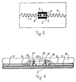
- the result in Fig. 3 is shown in the form of a plan view of the resulting circuit substrate, the film 1 is structured by photolithography or other suitable method so that it forms a conductor pattern with stretchable interconnects 7, which are each connected to a pad 8.
- An extensibility of the tracks 7 is achieved in that they are formed with a meandering or undulating course and thus have an excess length due to which they can be extended under tension without breakage.
- Reinforcing structures 9 which were formed during patterning from the conductive film 1 and stiffen the substrate layer and thus the resulting stretchable circuit carrier in an environment of the connection surfaces 8 can also be seen.
- the stiffening structures 9 are In this case, stiffening surfaces (stiffening pads) which are insulated from the conductor tracks 7 and the connection surfaces 8 and span a distance between the connection surfaces 8 without touching them, wherein the two connection surfaces 8 lie between two such stiffening pads.
- the conductor structure with a in the Fig. 4 recognizable electronic component 10 may be, which may be a sensor, an integrated circuit or a surface mounted device (SMD). It would be possible to mount this electronic component 10 in a manner known per se directly on the connection surfaces 8, for example by means of a conductive adhesive. In the present embodiment, however, the electronic component 10 is first attached to two additional surfaces which have been left standing in the patterning of the film 1, after which terminals 11 of the electronic component 10 by means of a conductive stretchable material 12, in the present example filled with conductive particles or fibers Plastic, are connected to the pads 8.
- a conductive stretchable material 12 in the present example filled with conductive particles or fibers Plastic
- the electronic component 10 is surrounded with another material 13, which is a polymer material which is poured over the electronic component 10 and after curing is stiffer than the stretchable substrate layer 5.
- another material 13 which is a polymer material which is poured over the electronic component 10 and after curing is stiffer than the stretchable substrate layer 5.
- a the electronic component 10 and the conductor structure with the conductor tracks 7 and the pads 8 overlapping second stretchable layer 14 applied which is again formed here of a thermoplastic polyurethane, which at a temperature of at most 130 ° C in liquefied form can be applied without destroying the electronic component 10 and its contacts.
- the starting material 3 used in the present example has a melting temperature of about 200 ° C, so that the stretchable substrate layer 5 does not flow when applying the second stretchable layer 14.
- an extensible circuit carrier has arisen, which can easily be extended several times to a length of approximately 150% of an initial length and can be relaxed again to the initial length.
- an expandable circuit carrier is produced comprising electronic components 10, thus forming an autonomous overall electronic system.
- Recurring features are in the FIGS. 5 to 8 again provided with the same reference numerals and have comparable properties, unless otherwise expressly stated.
- the film 1 is first provided by exposure to laser radiation 15 with position markings 16, which are given by depressions, as well as with orientation holes 17.
- This process step is in Fig. 5 illustrated.
- electronic components 10 which are present here in SMD design, are arranged with terminals 11 on the position markings 16 and thus also in a defined position relative to the orientation bores 17 on the conductive film 1 and connected in the present example by soldering to the film 1.
- the electronic components 10 instead, for example, by pressure welding, diffusion bonding or gluing be connected by means of a conductive adhesive to the film 1.
- the so connected to the film 1 electronic components 10 are then surrounded with a polymer material 13 and thereby fixed mechanically stable on the film 1.
- a stretchable substrate layer 5 which in this case has a thickness of about 100 .mu.m, wherein compared to this stretchable substrate layer 5, the material surrounding the electronic components 10 13 is stiffer.
- the film 1 now acts again in a conventional manner, so for example by photolithography, structured so that it forms a conductor structure with stretchable tracks 7 and pads 8, the orientation holes 15 serve as orientations in which the again meandering guided tracks 7 and the connection surfaces 8 are arranged in a defined position relative to the orientation bores 17.
- FIG. 1 illustrates a conductive stretchable material 12 which connects the terminals 11 of the electronic components 10 to the pads 8 and which could be applied locally prior to applying the stiffer material 13 or after structuring the film 1.
- second stretchable layer 14 is applied, after which the conductor structure is embedded in a now the stretchable substrate layer 5 and the second stretchable layer 14 comprehensive stretchable substrate.
- FIGS. 1 to 4 described method so with the basis of FIGS. 5 to 8 in the latter, before the second extensible layer 14 is applied, at least one further electronic component (10) is mounted on the conductor structure on a side of the film 1 facing away from the extensible substrate layer 5; Fig. 8 is shown with a dotted outline.
- an expandable circuit carrier which can be produced in the manner described can be shown, which can be, for example, an autonomous electronic system with sensor function for medical technology applications.
- the present invention thus proposes an advantageously simple method for producing a stretchable circuit substrate, in which a conductor structure is connected to a stretchable substrate layer, wherein the conductor pattern is formed such that it has extensible conductor tracks and terminal pads respectively connected to one of the extensible conductor tracks for at least an electronic component comprises.
- a preferred embodiment of the invention provides that a starting material for the substrate layer is applied to an electrically conductive film and connected to the film to form the expandable substrate layer, after which the Film is patterned so that it forms the conductor pattern, wherein also reinforcing structures are structured in the film, which stiffen the substrate layer in an environment of at least two pads without electrically connecting the pads together, thereby it is easy to prevent a electrical contact of a mounted on the pads electronic component in a stretching or relaxing the circuit substrate is damaged.
- a correspondingly advantageously expandable circuit carrier which can be produced by this method, comprises a stretchable substrate, a conductor structure embedded in the substrate or arranged on a surface of the substrate with stretchable interconnects and at least two connection surfaces respectively connected to one of the interconnects and at least one electronic component having terminals electrically conductively connected to the pads, the conductor pattern having in a plane with the tracks and formed of the same material as the tracks reinforcing structures stiffen the circuit carrier in an environment of the connected to the at least one electronic component pads, without connecting the pads electrically conductive together.
- circuit carrier is to be understood in such a way that it also includes - here stretchable - circuits that have in addition to a stretchable circuit board mounted or integrated electronic components.
Description
Die vorliegende Erfindung betrifft ein Verfahren zum Herstellen eines dehnbaren Schaltungsträgers sowie einen entsprechenden dehnbaren Schaltungsträger.The present invention relates to a method for manufacturing a stretchable circuit carrier and a corresponding stretchable circuit carrier.
Dehnbare Schaltungsträger können insbesondere im medizintechnischen Bereich Anwendung finden, wenn es gilt, Schaltungsträger und gegebenenfalls mit den Schaltungsträgern verbundene elektronische Bauteile beispielsweise an oder in einem lebenden Körper an Oberflächen mit dreidimensionaler Topographie anzuordnen. Weiter Anwendungen können sich durch eine Integration von Schaltungsträgern in designerisch anspruchsvollen Umgebungen, beispielsweise in Fahrzeuginnenräumen, ergeben.Stretchable circuit carriers can be used in particular in the field of medical technology if it is necessary to arrange circuit carriers and, if appropriate, electronic components connected to the circuit carriers, for example on or in a living body on surfaces with a three-dimensional topography. Further applications may result from an integration of circuit boards in designerisch demanding environments, such as in vehicle interiors.
Dehnbare Schaltungsträger sind z.B. aus der Druckschrift
Diese Aufgabe wird erfindungsgemäß gelöst durch ein Verfahren mit den Merkmalen des Anspruchs 1 sowie durch einen dehnbaren Schaltungsträger mit den Merkmalen des Anspruchs 17. Vorteilhafte Ausgestaltungen und Weiterentwickelungen der Erfindung ergeben sich mit den Merkmalen der Unteransprüche.This object is achieved by a method having the features of
Das vorgeschlagene Verfahren lässt sich dadurch sehr einfach durchführen, dass ein Ausgangsmaterial für ein dehnbares Substrat auf eine zunächst vollflächig vorliegende Folie aufgebracht wird, welches dann eine mit der Folie verbundene, also auf der Folie haftende, dehnbare Substratschicht bildet, wonach die Folie so strukturiert wird, dass sie eine Leiterstruktur mit mindestens einer dehnbaren Leiterbahn bildet.The proposed method can be carried out very simply by applying a starting material for a stretchable substrate to a film which is initially present over the entire area, which then forms an extensible substrate layer bonded to the film, ie adhering to the film, after which the film is structured in that it forms a conductor structure with at least one extensible conductor track.
Dabei kann die Substratschicht durch Verwendung eines entsprechenden Ausgangsmaterials, das auch aus mehreren Komponenten bestehen kann, insbesondere aus einem vorzugsweise thermoplastischen Polyurethan oder aus Silikon oder Kautschuk oder Latex oder einem anderen dehnbaren, gummiartigen Polymer gebildet werden. Das Bilden der dehnbaren Substratschicht kann dabei durch ein Aushärten, beispielsweise ein Vernetzen oder Abbinden, des Ausgangsmaterials geschehen, bei dem dieses in einen dehnbaren Endzustand übergeht. Das Aushärten kann bei verschiedenen Ausführungen der Erfindung thermisch oder chemisch ausgelöst werden. In einem besonders einfachen Fall wird ein thermoplastisches Ausgangsmaterial zum Bilden der Substratschicht verwendet, das durch Auskühlen aushärtet und in seinen dehnbaren Endzustand übergeht.In this case, the substrate layer by use of a corresponding starting material, which may also consist of several components, in particular of a preferably thermoplastic polyurethane or of silicone or rubber or latex or another elastic, rubbery polymer are formed. The forming of the stretchable substrate layer can be done by curing, for example, crosslinking or setting, of the starting material, in which this passes into a stretchable final state. The curing can be triggered thermally or chemically in various embodiments of the invention. In a particularly simple case, a thermoplastic starting material is used to form the substrate layer, which cures by cooling and transitions to its final stretchable state.
Die dehnbare Substratschicht kann dabei beispielsweise eine vorzugsweise gleichmäßige Dicke von zwischen 25 µm und 1 mm erhalten, wobei sich eine vorteilhaft leichte Dehnbarkeit bei nicht zu geringer Belastbarkeit insbesondere dann ergeben kann, wenn die dehnbare Substratschicht mit einer Dicke von zwischen 25 µm und 200 µm ausgeführt wird. In beschriebener Weise ist es problemlos möglich, eine Substratschicht und damit einen Schaltungsträger zu realisieren, die sich um mindestens 10 %, vorzugsweise um mindestens 50 %, das heißt auf mindestens 110 % bzw. 150 % einer Ausgangslänge, ausdehnen lassen, wobei auch ein mehrfaches Dehnen und Entspannen der Schaltungsträgers keine Beschädigungen bewirkt.The stretchable substrate layer can, for example, a preferably uniform thickness of between 25 .mu.m and 1 mm obtained, with an advantageously easy elasticity at not too low load capacity can result in particular when the stretchable substrate layer with a thickness of between 25 .mu.m and 200 .mu.m becomes. In the manner described, it is easily possible to realize a substrate layer and thus a circuit carrier which can be extended by at least 10%, preferably by at least 50%, ie to at least 110% or 150% of an initial length, wherein a multiple Stretching and relaxing the circuit board causes no damage.
Das Ausgangsmaterial zum Bilden der dehnbaren Substratschicht kann in einfacher Weise durch Rakeln oder Drucken, insbesondere durch Siebdruck, der wiederum mit Hilfe eines Rakels durchgeführt werden kann, oder durch Gießen oder Laminieren auf die Folie aufgebracht werden. Im Fall eines Aufbringens des Ausgangsmaterials durch Laminieren kann das Ausgangsmaterial beispielsweise in Form von Pulver oder auch in Folienform auf die die Leiterstruktur bildende Folie aufgetragen werden, um dann vorzugsweise unter Einwirkung von Druck und/oder Temperatur - beispielsweise mittels einer Walze (durch Rollenlaminieren) -, mit der leitenden Folie verbunden zu werden.The starting material for forming the stretchable substrate layer can be easily applied to the film by doctoring or printing, in particular by screen printing, which in turn can be carried out with the aid of a doctor blade, or by casting or laminating. In the case of applying the starting material by lamination, the starting material may be, for example, in the form of powder or in film form on the film forming the conductor pattern be applied, and then preferably under the action of pressure and / or temperature - for example by means of a roller (by roll lamination) - to be connected to the conductive film.
Um eine bessere Haftung der dehnbaren Substratschicht auf der leitenden Folie zu erreichen, kann die Folie vor dem Auftragen des Ausgangsmaterials an einer später der Substratschicht zugewandten Oberfläche chemisch oder mechanisch aufgerauht und/oder oxidiert werden.In order to achieve a better adhesion of the stretchable substrate layer on the conductive film, the film may be roughened and / or oxidized chemically or mechanically before the application of the starting material to a later surface facing the substrate layer.
Die leitende Folie, die mit Blick auf eine gute Leitfähigkeit aus Kupfer oder auch aus Gold oder Silber oder einem anderen Metall gebildet sein kann, kann im Hinblick auf möglichst geringe Abmessungen des Schaltungsträgers bei einer nicht zu großen Empfindlichkeit der mindestens einen Leiterbahn beispielsweise mit einer Dicke von zwischen 5 µm und 100 µm gewählt werden. Das Strukturieren dieser Folie zum Bilden der Leiterstruktur kann dabei in an sich bekannter Weise geschehen, beispielsweise durch Photolithographie. Um zu gewährleisten, dass die mindestens eine Leiterbahn dehnbar ist, kann es vorgesehen sein, dass die Leiterbahn dabei einen alternierend in einander gegenüberliegende Richtungen aus einer Hauptleiterrichtung herausgekrümmten, also typischerweise einen wellenförmigen, zickzack-förmigen oder mäanderförmigen Verlauf erhält. Um ein Brechen der mindestens einen Leiterbahn bei einem Dehnen des so hergestellten Schaltungsträgers zu vermeiden, sollten Richtungsänderungen des Verlaufs der Leiterbahnen dabei möglichst gerundet geformt sein.The conductive foil, which may be formed with a view to a good conductivity of copper or of gold or silver or another metal, with regard to the smallest possible dimensions of the circuit substrate with a not too high sensitivity of at least one conductor track, for example, with a thickness be chosen between between 5 microns and 100 microns. The structuring of this film to form the conductor structure can be done in a conventional manner, for example by photolithography. In order to ensure that the at least one conductor track is stretchable, it may be provided that the conductor track thereby curves out of a main conductor direction in an alternating manner in opposite directions, that is to say typically receives a wave-shaped, zigzag-shaped or meandering course. In order to avoid a breakage of the at least one conductor track during a stretching of the circuit substrate thus produced, changes in the direction of the conductor tracks should be formed as rounded as possible.
Es kann vorgesehen sein, dass nach dem Strukturieren der Folie eine die Leiterstruktur überdeckende zweite dehnbare Schicht auf die Leiterstruktur und auf freigelegte Bereiche der zuerst genannten dehnbaren Substratschicht aufgebracht wird, die dadurch mit der dehnbaren Substratschicht zusammen ein Substrat bildet, in dem die Leiterstruktur eingebettet und so geschützt liegt. Zur Herstellung der zweiten dehnbaren Schicht können dabei wieder alle weiter oben als mögliche Ausgangsmaterialien für die dehnbare Substratschicht genannten Materialien verwendet werden. Dabei kann das gleiche oder ein anderes Material verwendet werden als für die dehnbare Substratschicht. Zum Auftragen des entsprechenden Materials kommen die schon genannten Verfahren in Frage, also insbesondere Drucken, Rakeln, Gießen oder Laminieren.It can be provided that, after the structuring of the film, a second structure covering the conductor structure stretchable layer is applied to the conductor structure and to exposed portions of the first-mentioned stretchable substrate layer, which together with the stretchable substrate layer together forms a substrate in which the conductor structure is embedded and thus protected. For the production of the second stretchable layer, all materials mentioned above as possible starting materials for the stretchable substrate layer can again be used. In this case, the same or a different material can be used as for the stretchable substrate layer. For applying the appropriate material, the already mentioned methods are suitable, in particular printing, knife coating, casting or lamination.
Erfindungsgemäß umfasst die Leiterstruktur neben der mindestens einen Leiterbahn - normalerweise werden mehrere dehnbare Leiterbahnen vorgesehen sein - auch Anschlussflächen, die zum Kontaktieren von mit der Leiterstruktur zu verbindenden elektronischen Bauelementen geeignet sind. Dabei ist es besonders vorteilhaft, dass zusätzlich zu den Leiterbahnen mit den Anschlussflächen, die jeweils mit einer dehnbaren Leiterbahn verbunden sind, Verstärkungsstrukturen in die Folie einstrukturiert werden, die die Substratschicht in einer Umgebung mindestens zweier Anschlussflächen versteifen, ohne diese Anschlussflächen elektrisch miteinander zu verbinden. Dabei kann eine mechanische Überbelastung von elektrischen Verbindungen zwischen den Anschlussflächen und Anschlüssen eines mit den Anschlussflächen kontaktierten elektronischen Bauelements und eine den Kontakt unterbrechende Beschädigung dieser Verbindungen vermieden werden. Bei den Verstärkungsstrukturen kann es sich dabei beispielsweise um VersteifungsPads oder Versteifungsflächen handeln, die in der Umgebung der entsprechenden Anschlussflächen angeordnet und vorzugsweise ringsherum isoliert sind.According to the invention, the conductor structure comprises, in addition to the at least one conductor track-normally a plurality of extensible conductor tracks are provided-also connection surfaces which are suitable for contacting electronic components to be connected to the conductor structure. In this case, it is particularly advantageous that, in addition to the strip conductors with the connection surfaces, which are each connected to an extensible strip, reinforcement structures are structured in the film, stiffening the substrate layer in an environment of at least two pads, without electrically connecting these pads together. In this case, a mechanical overloading of electrical connections between the pads and terminals of a contacted with the pads electronic component and a contact interrupting damage to these compounds can be avoided. The reinforcement structures may be, for example, stiffening pads or stiffening surfaces that are in the environment the corresponding pads are arranged and preferably insulated around it.
Eine vorteilhafte Ausgestaltung des Verfahrens sieht vor, dass der damit hergestellte Schaltungsträger mindestens ein mit der Leiterstruktur verbundenes elektronisches Bauelement umfasst und so eine dehnbare komplexe elektronische Struktur bildet. Dabei können verschiedene elektronische Bauelemente verwendet werden, beispielsweise aktive oder passive oberflächenmontierte Bauelemente oder in Flip-Chip-Technik montierte integrierte Schaltkreise. Auch kann es sich bei dem mindestens einen elektronischen Bauelement um einen Sensor handeln.An advantageous embodiment of the method provides that the circuit carrier produced therewith comprises at least one electronic component connected to the conductor structure and thus forms an extensible complex electronic structure. In this case, various electronic components can be used, for example active or passive surface-mounted components or flip-chip technology mounted integrated circuits. Also, the at least one electronic component may be a sensor.
Ein solches elektronisches Bauelement kann auf verschiedene Weisen in den dehnbaren Schaltungsträger integriert werden. Beispielsweise kann es vorgesehen sein, dass die Leiterstruktur nach dem Strukturieren der Folie mit dem mindestens einen elektronischen Bauelement bestückt wird, wobei eine Verbindung mit der Leiterstruktur in an sich bekannter Weise, beispielsweise mittels eines leitfähigen Klebstoffs, geschehen kann. In diesem Fall ist es besonders vorteilhaft, wenn anschließend eine die Leiterstruktur überdeckende zweite dehnbare Schicht aufgebracht wird, in die dann auch das mindestens eine elektronische Bauelement teilweise oder vollständig eingebettet werden kann. Um Kontaktierungen zwischen dem elektronischen Bauelement und der Leiterstruktur vor Überlastungen bei einem Dehnen des dehnbaren Schaltungsträgers zu schützen, kann das elektronische Bauelement nach einem Kontaktieren mit der Leiterstruktur mit einem Material umgeben werden, welches das elektronische Bauelement mit der dehnbaren Substratschicht und der Leiterstruktur in einer Umgebung des elektronischen Bauelements verbindet und das, gegebenenfalls nach einem Aushärten, steifer ist als die dehnbare Substratschicht. Dazu kann das elektronische Bauelement beispielsweise mit dem genannten Material umgossen werden. Die genannte zweite dehnbare Schicht kann gegebenenfalls anschließend aufgebracht werden. Auch das genannte steifere Material wird dabei üblicherweise durch ein Polymer gegeben sein.Such an electronic component can be integrated in various ways in the expandable circuit carrier. For example, it may be provided that the conductor structure is equipped after structuring the film with the at least one electronic component, wherein a connection with the conductor structure in a conventional manner, for example by means of a conductive adhesive, can be done. In this case, it is particularly advantageous if subsequently a second stretchable layer covering the conductor structure is applied, into which the at least one electronic component can then also be partially or completely embedded. In order to protect contacts between the electronic component and the conductor structure against overloading during expansion of the expandable circuit carrier, the electronic component can be surrounded after contacting with the conductor structure with a material which surrounds the electronic component with the expandable substrate layer and the conductor structure in an environment of electronic component connects and that, optionally after curing, is stiffer than the stretchable substrate layer. For this purpose, the electronic component can be encapsulated, for example, with said material. The said second extensible layer may optionally be subsequently applied. The said stiffer material will usually be given by a polymer.
Wenn die Leiterstruktur in beschriebener Weise nach dem Strukturieren der Folie mit dem elektronischen Bauelement oder mehreren Bauelementen bestückt wird und eine anschließend aufgebrachte, die Leiterstruktur überdeckende zweite dehnbare Schicht vorgesehen ist, kann es vorteilhaft sein, die zweite dehnbare Schicht bei einer niedrigeren Temperatur aufzubringen als das die Substratschicht bildende Ausgangsmaterial. So kann es beispielsweise vorgesehen sein, als Ausgangsmaterial für die dehnbare Substratschicht ein Thermoplast einer Schmelztemperatur von größer als 200° C zu verwenden, während die zweite dehnbare Schicht aus einem thermoplastischen Kunststoff mit einer Schmelztemperatur von weniger als 130° C gebildet wird. Dadurch kann erreicht werden, dass einerseits die dehnbare Substratschicht beim Bestücken der Leiterstruktur mit dem elektronischen Bauelement nicht beschädigt wird - selbst dann, wenn dazu beispielsweise ein Lötprozess durchgeführt wird -, während andererseits durch die niedrigere Temperatur beim Aufbringen der zweiten dehnbaren Schicht eine Beschädigung der Verbindung des elektronischen Bauelements mit der Leiterstruktur verhindert wird. In dieser Hinsicht ist es besonders vorteilhaft, wenn die dehnbare Substratschicht Temperaturen von etwa 200° C beschädigungsfrei aushalten kann, während die zweite dehnbare Schicht bei einer Temperatur von höchstens 130° C aufgetragen wird.If the conductor structure in the manner described after the structuring of the film with the electronic component or a plurality of components is equipped and a subsequently applied, the conductor structure overlapping second stretchable layer is provided, it may be advantageous to apply the second stretchable layer at a lower temperature than that the substrate layer forming starting material. For example, it may be provided to use a thermoplastic having a melting temperature greater than 200 ° C. as the starting material for the expandable substrate layer, while the second expandable layer is formed from a thermoplastic having a melting point of less than 130 ° C. It can thereby be achieved that, on the one hand, the expandable substrate layer is not damaged when the conductor structure is fitted with the electronic component-even if, for example, a soldering process is carried out-and, on the other hand, because of the lower temperature during the application of the second stretchable layer the electronic component is prevented with the conductor structure. In this regard, it is particularly advantageous if the stretchable substrate layer can withstand temperatures of about 200 ° C without damage, while the second stretchable layer at a temperature of 130 ° C is applied.
Ein anderes Verfahren zur Realisierung eines dehnbaren Schaltungsträgers mit mindestens einem elektronischen Bauelement sieht vor, dass schon vor dem Aufbringen des Ausgangsmaterials auf die Folie das mindestens eine elektronische Bauelement so auf der Folie angeordnet und mit der Folie verbunden wird, dass das mindestens eine elektronische Bauelement beim Aufbringen des Ausgangsmaterials zumindest teilweise in die entstehende dehnbare Substratschicht eingebettet wird, wobei das Ausgangsmaterial das elektronische Bauelement vorzugsweise vollständig überdecken sollte. Eine leitende Verbindung von Anschlüssen des elektronischen Bauelements mit der Folie kann dabei wieder in an sich bekannter Weise hergestellt werden, beispielsweise durch Ankleben mit einem leitfähigen Klebstoff oder auch durch Anlöten oder Anschweißen, insbesondere durch Pressschweißen oder Diffusionsbonden. Vorteilhafter Weise kann dabei auch bei einer Anwendung höherer Temperaturen beim Verbinden des elektronischen Bauelements mit der Folie keine Beschädigung der dehnbaren Substratschicht erfolgen, weil diese erst später aufgetragen wird. Das Strukturieren der Folie zum Herstellen der Leiterstruktur geschieht dagegen wieder erst nach dem Aufbringen der dehnbaren Substratschicht, wobei die Leiterstruktur wiederum dadurch geschützt werden kann, dass anschließend noch eine die Leiterstruktur überdeckende zweite dehnbare Schicht aufgebracht wird.Another method for realizing an expandable circuit carrier having at least one electronic component provides that even before the application of the starting material to the film, the at least one electronic component is arranged on the film and connected to the film, that the at least one electronic component in the Application of the starting material is at least partially embedded in the resulting expandable substrate layer, wherein the starting material should preferably completely cover the electronic component. A conductive connection of terminals of the electronic component with the film can be made again in a conventional manner, for example by gluing with a conductive adhesive or by soldering or welding, in particular by pressure welding or diffusion bonding. Advantageously, no damage can be done to the stretchable substrate layer even when using higher temperatures when connecting the electronic component to the film because it is applied later. On the other hand, the structuring of the foil for producing the conductor structure takes place again only after the application of the extensible substrate layer, wherein the conductor structure can again be protected by subsequently applying a second extensible layer covering the conductor structure.
Wenn bei dem im vorherigen Absatz beschriebenen Verfahren das mindestens eine auf der Folie angeordnete elektronische Bauelement vor dem Aufbringen des Ausgangsmaterials zur Bildung der dehnbaren Substratschicht mit einem Material umgeben wird, das das elektronische Bauelement mechanisch mit der Folie verbindet und das - gegebenenfalls nach einem Aushärten - steifer ist als die dehnbare Substratschicht, kann wieder in einfacher Weise ein Schutz von Kontaktierungen zwischen dem elektronischen Bauelement und der später entstehenden Leiterstruktur vermieden werden. Bei einer vorteilhafter Ausgestaltung des Verfahrens kann vorgesehen sein, dass die Folie vor dem Anordnen des mindestens einen elektronischen Bauelements auf der Folie mit beispielsweise durch Vertiefungen gegebenen Positionsmarkierungen und/oder mit Orientierungsbohrungen versehen wird, beispielsweise durch eine Behandlung mit Laserstrahlung, wonach das mindestens eine elektronische Bauelement an den Positionsmarkierungen und/oder in definierter Position relativ zu den Orientierungsbohrungen angeordnet wird. Das kann eine richtige Anordnung des elektronischen Bauelements oder der elektronischen Bauelemente erleichtern angesichts der Tatsache, dass die Leiterstruktur dann noch nicht fertiggestellt ist. Geeignet geformte Positionsmarkierungen können dabei - insbesondere bei einem Lötprozess - in vorteilhafter Weise auch eine Selbstzentrierung des elektronischen Bauelements beim Verbinden mit der Folie bewirken. Orientierungsbohrungen, die die Folie vollständig durchstoßen oder zumindest an einer Rückseite der Folie erkennbar sind, können ferner in vorteilhafter Weise beim Strukturieren der Folie zur Bildung der Leiterstruktur als Orientierung dienen.In the method described in the previous paragraph, if the at least one electronic component disposed on the foil is surrounded with a material prior to the application of the starting material to form the expansible substrate layer, said material is surrounded by the material mechanically connects the electronic component with the film and - if necessary after curing - is stiffer than the stretchable substrate layer, can be avoided again in a simple way a protection of contacts between the electronic component and the later resulting conductor structure. In an advantageous embodiment of the method can be provided that the film is provided prior to arranging the at least one electronic component on the film with, for example, by recesses given position marks and / or with orientation holes, for example by treatment with laser radiation, after which the at least one electronic Component is arranged on the position marks and / or in a defined position relative to the orientation holes. This may facilitate proper placement of the electronic component or components in view of the fact that the conductor pattern is not yet completed. In this case, suitably shaped position markings-in particular in the case of a soldering process-can advantageously also bring about self-centering of the electronic component when it is connected to the film. Orientation holes that completely pierce the film or that are recognizable at least at a backside of the film may also advantageously serve as an orientation in patterning the film to form the conductor pattern.
Unter Umständen ist es auch möglich, die zwei verschiedenen zum Integrieren von elektronischen Bauelementen in oder auf einem dehnbaren Schaltungsträgersubstrat beschriebenen Verfahren so zu kombinieren, dass ein elektronisches Bauelement oder mehrere elektronische Bauelemente vor dem Aufbringen des Ausgangsmaterials zum Bilden der dehnbaren Substratschicht mit der noch unstrukturierten Folie verbunden und anschließend in die dehnbare Substratschicht eingebettet werden, während mindestens ein weiteres elektronisches Bauelement nach dem Strukturieren der Folie auf der Gegenüberliegenden Seite mit der Leiterstruktur verbunden und gegebenenfalls durch eine zweite dehnbare Schicht überdeckt wird.It may also be possible to combine the two different methods described for integrating electronic components in or on a stretchable circuit substrate, such that one or more electronic components prior to application of the starting material for forming the stretchable substrate layer are connected to the still unstructured film and then embedded in the stretchable substrate layer, while at least one further electronic component is connected to the conductor structure after structuring the film on the opposite side and optionally covered by a second stretchable layer.
Unabhängig von dem gewählten Verfahren können schließlich Anschlüsse des mindestens einem elektronischen Bauelements nicht nur direkt, sondern auch mittels eines leitfähigen dehnbaren Materials mit Anschlussflächen (Pads genannt) der Leiterstruktur verbunden werden. Im Fall einer Montage des elektronischen Bauelements auf der noch nicht strukturierten Folie kann das wiederum vor dem Aufbringen des Ausgangsmaterials für die dehnbare Substratschicht - das gilt insbesondere für den Fall, dass das elektronische Bauelement der Folie abgewandte Anschlüsse aufweist - oder nach einem Strukturieren der Folie geschehen. Eine dadurch erreichte elastische Kontaktierung des elektronischen Bauelements kann eine Beschädigung der leitenden Verbindung des elektronischen Bauelements mit der Leiterstruktur bei einem Dehnen des dehnbaren Schaltungsträgers vermeiden helfen. Bei dem leitfähigen dehnbaren Material kann es sich beispielsweise um einen mit leitenden Partikeln oder Fasern gefüllten gummiartigen Kunststoff handeln.Finally, regardless of the method chosen, terminals of the at least one electronic component can be connected not only directly but also by means of a conductive, expansible material with pads (called pads) of the conductor structure. In the case of a mounting of the electronic component on the not yet structured film, this in turn can be done before the application of the starting material for the stretchable substrate layer - this is especially true in the case where the electronic component facing away from the film - or after a patterning of the film , An elastic contacting of the electronic component achieved thereby can help prevent damage to the conductive connection of the electronic component to the conductor structure when the expandable circuit substrate is stretched. The conductive stretchable material may be, for example, a rubbery plastic filled with conductive particles or fibers.
Besonders vorteilhafte dehnbare Schaltungsträger, die sich beispielsweise in beschriebener Weise herstellen lassen, umfassen demnach ein dehnbares Substrat, eine in das Substrat eingebettete oder an einer Oberfläche des Substrats angeordnete Leiterstruktur mit dehnbaren Leiterbahnen und mindestens zwei jeweils mit einer der Leiterbahnen verbundenen Anschlussflächen sowie mindestens ein elektronisches Bauelement, das mit den Anschlussflächen elektrisch leitend verbundene Anschlüsse aufweist, wobei die Leiterstruktur Verstärkungsstrukturen aufweist, die den Schaltungsträger in einer Umgebung der mit dem mindestens einen elektronischen Bauelement verbundenen Anschlussflächen versteift, ohne die Anschlussflächen elektrisch zu verbinden. Zusätzlich kann er vorgesehen sein, dass
- das mindestens eine elektronische Bauelement mit einem es mechanisch mit der Leiterstruktur verbindenden Material umgeben ist, das steifer ist als das ein das dehnbare Substrat bildendes Material, und/oder
- mindestens einer der Anschlüsse des mindestens einen elektronischen Bauelements mittels eines leitfähigen dehnbaren Materials mit der entsprechenden Anschlussfläche verbunden ist.
Die genannten Merkmale dienen dabei insbesondere dazu, Kontaktierungen zwischen dem mindestens einen elektronischen Bauelement und der Leiterstruktur vor Beschädigungen auch bei einem gegebenenfalls mehrfachen Dehnen und Relaxieren des dehnbaren Schaltungsträgers zu verhindern. Ein solcher dehnbarer Schaltungsträger kann zusätzlich selbstverständlich alle möglichen Kombinationen der Merkmale aufweisen, die sich aus den zuvor beschriebenen Ausgestaltungen des entsprechenden Herstellungsverfahrens ergeben.
Dehnbare Schaltungsträger der zuletzt beschriebenen Art können schließlich sogar vollständig dehnbare autonome elektronische Gesamtsysteme - beispielsweise Sensor, Prozessor, Datenübertragungsmittel und Energieversorgung umfassend - bilden und insbesondere dann besonders vorteilhaft sein, wenn eine Datenverarbeitung möglichst nah an einem Sensor erfolgen soll und eventuell anschließend ein drahtloser Datentransfer zu einer Kontrollstelle vorgesehen ist.
Ausführungsbeispiele der vorliegenden Erfindung werden nachfolgend anhand dervorliegenden Figuren 1 bis 8 beschrieben. Es zeigt- Fig. 1
- einen Querschnitt durch eine Kupferfolie bei einem ersten Schritt eines erfindungsgemäßen Verfahrens,
- Fig. 2
- in entsprechender Darstellung einen ersten Verfahrensschritt bei einer alternativen Gestaltung des Verfahrens,
- Fig. 3
- eine Aufsicht auf einen bei dem Verfahren entstehenden dehnbaren Schaltungsträger nach einem weiteren Verfahrensschritt,
- Fig. 4
- wieder einen Querschnitt durch denselben Schaltungsträger nach abschließenden Verfahrensschritten,
- Fig. 5
- einen Querschnitt durch eine Kupferfolie bei einem ersten Verfahrensschritt eines Verfahrens zum Herstellen eines dehnbaren Schaltungsträgers in einer anderen Ausführung der Erfindung,
- Fig. 6
- in entsprechender Darstellung den entstehenden Schaltungsträger nach darauf folgenden Verfahrensschritten desselben Verfahrens,
- Fig. 7
- denselben entstehenden Schaltungsträger nach einem Aufbringen einer dehnbaren Substratschicht und
- Fig. 8
- wieder eine Querschnittsdarstellung desselben entstehenden dehnbaren Schaltungsträgers nach einer Strukturierung der Kupferfolie.
- the at least one electronic component is surrounded by a material which mechanically bonds it to the conductor structure, which material is stiffer than the material forming the expandable substrate, and / or
- at least one of the terminals of the at least one electronic component is connected by means of a conductive stretchable material with the corresponding terminal surface.
The mentioned features are used in particular to prevent contacts between the at least one electronic component and the conductor structure from damage even with a possibly multiple stretching and relaxation of the stretchable circuit substrate. In addition, of course, such an expandable circuit carrier may have all possible combinations of the features that result from the previously described embodiments of the corresponding manufacturing method.
Finally, stretchable circuit carriers of the last-described type can even form completely expandable autonomous electronic overall systems-for example comprising sensor, processor, data transmission means and energy supply-and in particular be particularly advantageous if data processing as close as possible to a sensor and possibly then a wireless data transfer to a control point is provided.
Embodiments of the present invention will be described below with reference to the presentFIGS. 1 to 8 described. It shows- Fig. 1
- a cross section through a copper foil in a first step of a method according to the invention,
- Fig. 2
- in a corresponding representation, a first method step in an alternative embodiment of the method,
- Fig. 3
- a plan view of a resulting in the process expandable circuit carrier after a further process step,
- Fig. 4
- again a cross section through the same circuit carrier after final process steps,
- Fig. 5
- a cross section through a copper foil in a first method step of a method for producing a stretchable circuit substrate in another embodiment of the invention,
- Fig. 6
- in a corresponding representation of the resulting circuit substrate after subsequent steps of the same process,
- Fig. 7
- the same resulting circuit carrier after application of a stretchable substrate layer and
- Fig. 8
- again a cross-sectional view of the same resulting expandable circuit substrate after structuring of the copper foil.
In
Der beschriebene Verfahrensschritt kann auch in abgewandelter Form durchgeführt werden. Insbesondere kann das Ausgangsmaterial 3, wie in
In einem weiteren Verfahrensschritt, dessen Ergebnis in
Anschließend wird die Leiterstruktur mit einem in der
Im Anschluss daran wird das elektronische Bauelement 10 mit einem weiteren Material 13 umgeben, bei dem es sich um einen Polymeren Werkstoff handelt, der über das elektronische Bauelement 10 gegossen wird und nach einem Aushärten steifer ist als die dehnbare Substratschicht 5. In einem letzten Verfahrensschritt wird schließlich eine das elektronische Bauelement 10 und die Leiterstruktur mit den Leiterbahnen 7 und den Anschlussflächen 8 überdeckende zweite dehnbare Schicht 14 aufgebracht, die hier wieder aus einem thermoplastischen Polyurethan gebildet wird, das bei einer Temperatur von höchstens 130° C in verflüssigter Form aufgetragen werden kann, ohne das elektronische Bauelement 10 und dessen Kontaktierungen zu zerstören. Demgegenüber hat das im vorliegenden Beispiel verwendete Ausgangsmaterial 3 eine Schmelztemperatur von etwa 200° C, so dass auch die dehnbare Substratschicht 5 beim Aufbringen der zweiten dehnbaren Schicht 14 nicht verfließt. In beschriebener Weise ist ein dehnbarer Schaltungsträger entstanden, der sich problemlos auch mehrfach auf eine Länge von etwa 150 % einer Ausgangslänge ausdehnen und wieder auf die Ausgangslänge entspannen lässt.Thereafter, the
Auch bei dem in den
Bei diesem Verfahren wird die Folie 1 zunächst durch Einwirkung mit Laserstrahlung 15 mit Positionsmarkierungen 16, die durch Vertiefungen gegeben sind, sowie mit Orientierungsbohrungen 17 versehen. Dieser Verfahrensschritt ist in
Anschließend wird in ähnlicher Weise, wie zuvor anhand der
So entsteht nach einem Aushärten des Ausgangsmaterials 3 eine dehnbare Substratschicht 5, die hier eine Dicke von etwa 100 µm hat, wobei im Vergleich zu dieser dehnbaren Substratschicht 5 das die elektronischen Bauelemente 10 umgebende Material 13 steifer ist. Die Folie 1 wirkt nun wieder in an sich bekannter Weise, also beispielsweise durch Photolithographie, so strukturiert, dass sie eine Leiterstruktur mit dehnbaren Leiterbahnen 7 und Anschlussflächen 8 bildet, wobei die Orientierungsbohrungen 15 als Orientierungen dienen, in dem die wieder mäanderförmig geführten Leiterbahnen 7 und die Anschlussflächen 8 in definierter Position relativ zu den Orientierungsbohrungen 17 angeordnet werden. Bei einer Weiterentwicklung des Verfahrens wäre es auch denkbar zur Kontaktierung der elektronischen Bauelemente 10 wieder zusätzlich, wie in
Schließlich wäre es auch denkbar, das anhand der
In
Mit der vorliegenden Erfindung wird also ein vorteilhaft einfaches Verfahren zum Herstellen eines dehnbaren Schaltungsträgers vorgeschlagen, bei dem eine Leiterstruktur mit einer dehnbaren Substratschicht verbunden wird, wobei die Leiterstruktur so gebildet wird, dass sie dehnbare Leiterbahnen sowie jeweils mit einer der dehnbaren Leiterbahnen verbundene Anschlussflächen für mindestens ein elektronisches Bauelement umfasst. Dabei sieht eine bevorzugte Ausführung der Erfindung vor, dass zur Bildung der dehnbaren Substratschicht ein Ausgangsmaterial für die Substratschicht auf eine elektrisch leitende Folie aufgebracht und mit der Folie verbunden wird, wonach die Folie so strukturiert wird, dass sie die Leiterstruktur bildet, wobei außerdem Verstärkungsstrukturen in die Folie einstrukturiert werden, die die Substratschicht in einer Umgebung von mindestens zwei Anschlussflächen versteifen, ohne die Anschlussflächen elektrisch miteinander zu verbinden, dadurch lässt sich in einfacher Weise verhindern, dass eine elektrische Kontaktierung eines auf den Anschlussflächen montierten elektronischen Bauelements bei einem Dehnen oder Entspannen des Schaltungsträgers Schaden nimmt.The present invention thus proposes an advantageously simple method for producing a stretchable circuit substrate, in which a conductor structure is connected to a stretchable substrate layer, wherein the conductor pattern is formed such that it has extensible conductor tracks and terminal pads respectively connected to one of the extensible conductor tracks for at least an electronic component comprises. In this case, a preferred embodiment of the invention provides that a starting material for the substrate layer is applied to an electrically conductive film and connected to the film to form the expandable substrate layer, after which the Film is patterned so that it forms the conductor pattern, wherein also reinforcing structures are structured in the film, which stiffen the substrate layer in an environment of at least two pads without electrically connecting the pads together, thereby it is easy to prevent a electrical contact of a mounted on the pads electronic component in a stretching or relaxing the circuit substrate is damaged.
Ein dementsprechend vorteilhafter dehnbarer Schaltungsträger, der sich mit diesem Verfahren herstellen lässt, umfasst ein dehnbares Substrat, eine in das Substrat eingebettete oder an einer Oberfläche des Substrats angeordnete Leiterstruktur mit dehnbaren Leiterbahnen und mindestens zwei jeweils mit einer der Leiterbahnen verbundenen Anschlussflächen sowie mindestens ein elektronisches Bauelement, das mit den Anschlussflächen elektrisch leitend verbundene Anschlüsse aufweist, wobei die Leiterstruktur in einer Ebene mit den Leiterbahnen liegende und aus dem gleichen Material wie die Leiterbahnen gebildete Verstärkungsstrukturen aufweist, die den Schaltungsträger in einer Umgebung der mit dem mindestens einen elektronischen Bauelement verbundenen Anschlussflächen versteifen, ohne die Anschlussflächen elektrisch leitend miteinander zu verbinden. Der Begriff "Schaltungsträger" sei dabei so allgemein verstanden, dass er auch - hier dehnbare - Schaltungen umfasst, die zusätzlich zu einer dehnbaren Leiterplatte darauf montierte oder integrierte elektronische Bauelemente aufweisen.A correspondingly advantageously expandable circuit carrier, which can be produced by this method, comprises a stretchable substrate, a conductor structure embedded in the substrate or arranged on a surface of the substrate with stretchable interconnects and at least two connection surfaces respectively connected to one of the interconnects and at least one electronic component having terminals electrically conductively connected to the pads, the conductor pattern having in a plane with the tracks and formed of the same material as the tracks reinforcing structures stiffen the circuit carrier in an environment of the connected to the at least one electronic component pads, without connecting the pads electrically conductive together. The term "circuit carrier" is to be understood in such a way that it also includes - here stretchable - circuits that have in addition to a stretchable circuit board mounted or integrated electronic components.
Claims (19)
- A method for manufacturing an extensible circuit carrier, with which a starting material (3) for an extensible substrate is deposited onto an electrically conductive foil (1) and forms an extensible substrate layer (5) connected to the foil (1), whereupon the foil (1) is structured such that it forms a conductor structure with at least one extensible strip conductor (7), characterised in that the conductor structure comprises connection surfaces (8) which are each connected to an extensible strip conductor (7), and wherein moreover reinforcement structures (9) are structured into the foil (1) and these reinforcement structures stiffen the substrate layer (5) in an environment of at least two connection surfaces (8), without electrically connecting the connection surfaces (8) to one another.
- A method according to claim 1, characterised in that the at least one strip conductor (7) obtains a course which is curved in an alternating manner, in directions opposite one another, out of a main conductor direction.
- A method according to one of the claims 1 or 2, characterised in that the conductive foil (1) has a thickness of between 5 µm and 100 µm and/or is formed from copper or silver or gold.
- A method according to one of the claims 1 to 3, characterised in that the foil (1) is roughened or oxidised before the deposition of the starting material (3) on surface (2) which later faces the extensible substrate layer (5).
- A method according to one of the claims 1 to 4, characterised in that the extensible substrate layer (5) is formed from a polyurethane or silicone or rubber or latex.
- A method according to one of the claims 1 to 5, characterised in that the extensible substrate (5) has a thickness of between 25 µm and 1 mm.
- A method according to one of the claims 1 to 6, characterised in that the starting material (3) is deposited onto the foil (1) by way of printing or doctoring or moulding/casting or laminating.
- A method according to one of the claims 1 to 7, characterised in that a second extensible layer (14) which covers the conductor structure is deposited after the structuring of the foil (1).
- A method according to one of the claims 1 to 8, characterised in that the conductor structure after the structuring of the foil (1) is provided with at least one electronic component (10).
- A method according to claim 9, characterised in that the electronic component (10) is subsequently surrounded by a material (13) which is stiffer than the extensible substrate layer (5)
- A method according to one of the claims 9 or 10, inasmuch as these relate to claim 8, characterised in that the second extensible layer (14) is deposited at a lower temperature than the starting material (3) forming the extensible substrate layer (5).
- A method according to one of the claims 1 to 8, characterised in that at least one electronic component (10) is arranged on the foil (1) and is connected to the foil (1), before depositing starting material (3), wherein the at least one electronic component (10) is embedded into the arising extensible substrate layer (5) on depositing the starting material (3).
- A method according to claim 12, characterised in that the at least one electronic component (10) arranged on the foil (1), before the deposition of the starting material (3) is surrounded by a material (13) which is stiffer than the extensible substrate layer (5).
- A method according to one of the claims 12 or 13, characterised in that the foil (1) before the arrangement of the at least one electronic component (10) on the foil (1) is provided with positioning markings (16) and/or orientation bores (17), whereupon the at least one electronic component (10) is arranged on the position markings (16) and/or in definitive positions relative to the orientation bores (17).
- A method according to one of the claims 9 to 14, characterised in that connections (11) of the at least one electronic component (10) are connected to connection surfaces (8) of the conductor structure by way of a conductive extensible material (12).
- A method according to one of the claims 9 to 15, characterised in that the at least one electrical component (10) is soldered on the foil (1) or on the conductor structure.
- An extensible circuit carrier, comprising an extensible substrate, a conductor structure with extensible strip conductors (7) and with at least two connections surfaces (8) which are each connected to one of the strip conductors (7), said conductor structure being embedded into the substrate or arranged on a surface of the substrate, and as well as at least one electronic component (10) which comprises connections (11) which are electrically conductively connected to the connection surfaces (8),
characterised in that,
the conductor structure comprises reinforcement structures (9) which stiffen the circuit carrier in an environment of the connection surfaces (8) connected to the at least one electronic component (10), without electrically connecting the connection surfaces (8) to one another. - An extensible circuit carrier according to claim 17, characterised in thatthe at least one electronic component (10) is surrounded by a material (13) which mechanically connects it to the conductor structure and which is stiffer that a material forming the extensible substrateand/orat least one of the connections (11) of the at least one electronic component (10) is connected to the respective connection surface (8) by way of a conductive, extensible material (12).
- An extensible circuit carrier according to one of the claims 17 or 18, manufacturable according to one of the claims 1 to 16.
Applications Claiming Priority (1)
| Application Number | Priority Date | Filing Date | Title |
|---|---|---|---|
| DE102006055576A DE102006055576A1 (en) | 2006-11-21 | 2006-11-21 | Method for manufacturing a stretchable circuit carrier and expandable circuit carrier |
Publications (3)
| Publication Number | Publication Date |
|---|---|
| EP1926355A2 EP1926355A2 (en) | 2008-05-28 |
| EP1926355A3 EP1926355A3 (en) | 2009-12-23 |
| EP1926355B1 true EP1926355B1 (en) | 2014-01-08 |
Family
ID=39106123
Family Applications (1)
| Application Number | Title | Priority Date | Filing Date |
|---|---|---|---|
| EP07076013.7A Active EP1926355B1 (en) | 2006-11-21 | 2007-11-21 | Method for manufacturing an extendable circuit support and extendable circuit support |
Country Status (3)
| Country | Link |
|---|---|
| US (1) | US8654536B2 (en) |
| EP (1) | EP1926355B1 (en) |
| DE (1) | DE102006055576A1 (en) |
Families Citing this family (32)
| Publication number | Priority date | Publication date | Assignee | Title |
|---|---|---|---|---|
| DE102008002532A1 (en) | 2008-06-19 | 2009-12-24 | Robert Bosch Gmbh | Method for producing an electronic assembly |
| EP2392198B1 (en) * | 2009-01-30 | 2018-08-22 | IMEC vzw | Stretchable electronic device and method of manufacturing thereof |
| PL2392196T3 (en) | 2009-01-30 | 2019-05-31 | Imec Vzw | Stretchable electronic device |
| DE102009016368A1 (en) * | 2009-04-07 | 2010-10-21 | Carl Freudenberg Kg | Circuit carrier with electrical conductors |
| WO2010146524A1 (en) * | 2009-06-19 | 2010-12-23 | Koninklijke Philips Electronics N.V. | Conformable electronic devices and methods for their manufacture |
| DE102009031568A1 (en) * | 2009-06-29 | 2010-12-30 | Fraunhofer-Gesellschaft zur Förderung der angewandten Forschung e.V. | Method for producing an electronic system, method for producing a free-form surface with such a system, as well as electronic system and free-form surfaces with such a system |
| DE102009031600A1 (en) * | 2009-07-07 | 2011-01-13 | Fraunhofer-Gesellschaft zur Förderung der angewandten Forschung e.V. | Photovoltaic module for use on roof to produce energy, has solar cells arranged on substrate, predominantly covered with expandable material and arranged in such manner that solar cells are partly spaced to each other |
| EP2355144A1 (en) | 2010-02-09 | 2011-08-10 | Nederlandse Organisatie voor toegepast -natuurwetenschappelijk onderzoek TNO | Component placement on flexible and/or stretchable substrates |
| DE102010034718B4 (en) | 2010-08-18 | 2017-11-30 | Deutsches Zentrum für Luft- und Raumfahrt e.V. | Stretchable substrate having a contact point between a polymer-based electrical conductor and another electrical conductor |
| EP2461658A1 (en) | 2010-12-03 | 2012-06-06 | Nederlandse Organisatie voor toegepast -natuurwetenschappelijk onderzoek TNO | Method and apparatus for assembling electric components on a flexible substrate as well as assembly of an electric component with a flexible substrate |
| GB2489508B8 (en) * | 2011-03-31 | 2016-03-16 | Plasyl Ltd | Improvements for electrical circuits |
| US9226402B2 (en) * | 2012-06-11 | 2015-12-29 | Mc10, Inc. | Strain isolation structures for stretchable electronics |
| US9247637B2 (en) * | 2012-06-11 | 2016-01-26 | Mc10, Inc. | Strain relief structures for stretchable interconnects |
| DE102013019723A1 (en) | 2012-12-12 | 2014-06-12 | Carl Freudenberg Kg | Luminous element installed in e.g. capacitive switch for describing switching state, has transparent light-conducting cladding layer that is coated on supporting portion, and configured to scatter and reflect light |
| JP6518451B2 (en) | 2015-02-02 | 2019-05-22 | 株式会社フジクラ | Elastic circuit board |
| CN107210269B (en) | 2015-03-11 | 2020-07-28 | 英特尔公司 | Stretchable electronic device fabrication methods utilizing strain redistribution layers |
| US9572261B2 (en) | 2015-03-25 | 2017-02-14 | Texas Instruments Incorporated | Conductive through-polymer vias for capacitative structures integrated with packaged semiconductor chips |
| WO2017017127A1 (en) | 2015-07-28 | 2017-02-02 | At & S Austria Technologie & Systemtechnik Aktiengesellschaft | Stretchable electronic component carrier |
| JP6706324B2 (en) * | 2015-09-11 | 2020-06-03 | サイド・タイムール・アフマド | Method for protecting electronic devices by selective deposition of polymer coatings |
| JPWO2017047519A1 (en) * | 2015-09-17 | 2018-07-05 | 積水ポリマテック株式会社 | Elastic wiring material |
| DE112015006957T5 (en) * | 2015-09-24 | 2018-06-07 | Intel Corporation | Stretchable electronic arrangement |
| FI20165054A (en) * | 2016-01-28 | 2017-07-29 | Clothing Plus Mbu Oy | Flexible PCB |
| JP2018014381A (en) * | 2016-07-20 | 2018-01-25 | 富士通株式会社 | Substrate and electronic apparatus |
| US20180061578A1 (en) * | 2016-09-01 | 2018-03-01 | Apple Inc. | Stacked passive component structures |
| JP6972523B2 (en) * | 2016-09-13 | 2021-11-24 | セイコーエプソン株式会社 | Electronics |
| JP6776840B2 (en) * | 2016-11-21 | 2020-10-28 | オムロン株式会社 | Electronic devices and their manufacturing methods |
| WO2018168734A1 (en) * | 2017-03-13 | 2018-09-20 | 株式会社村田製作所 | Resin structure with built-in electronic component and method for producing same |
| JP6903981B2 (en) * | 2017-03-23 | 2021-07-14 | セイコーエプソン株式会社 | Detection device |
| US20200132520A1 (en) * | 2017-07-14 | 2020-04-30 | Sony Corporation | Sensor and method of manufacturing sensor |
| FI20175818A1 (en) | 2017-09-14 | 2019-03-15 | Clothing Plus Mbu Oy | A system for transmitting electrical signals |
| JP6930681B2 (en) * | 2019-03-25 | 2021-09-01 | 株式会社村田製作所 | Elastic mounting board |
| AT526502B1 (en) * | 2023-03-23 | 2024-04-15 | Sendance Gmbh | Deformable object |
Family Cites Families (13)
| Publication number | Priority date | Publication date | Assignee | Title |
|---|---|---|---|---|
| DE3019207A1 (en) * | 1980-05-20 | 1981-11-26 | GAO Gesellschaft für Automation und Organisation mbH, 8000 München | CARRIER ELEMENT FOR AN IC CHIP |
| FR2673017A1 (en) * | 1991-02-18 | 1992-08-21 | Schlumberger Ind Sa | METHOD FOR MANUFACTURING AN ELECTRONIC MODULE FOR A MEMORY CARD AND ELECTRONIC MODULE THUS OBTAINED. |
| JPH06314877A (en) * | 1993-04-30 | 1994-11-08 | Mitsui Toatsu Chem Inc | Manufacture of long-sized double-faced flexible metal laminated board |
| DE4410732C2 (en) * | 1994-03-28 | 1997-05-07 | Amatech Gmbh & Co Kg | Method for arranging a transponder unit having at least one chip and a wire coil on a substrate, as well as chip card with a correspondingly arranged transponder unit |
| US6654064B2 (en) * | 1997-05-23 | 2003-11-25 | Canon Kabushiki Kaisha | Image pickup device incorporating a position defining member |
| US6404643B1 (en) * | 1998-10-15 | 2002-06-11 | Amerasia International Technology, Inc. | Article having an embedded electronic device, and method of making same |
| US6606247B2 (en) * | 2001-05-31 | 2003-08-12 | Alien Technology Corporation | Multi-feature-size electronic structures |
| US7265298B2 (en) * | 2003-05-30 | 2007-09-04 | The Regents Of The University Of California | Serpentine and corduroy circuits to enhance the stretchability of a stretchable electronic device |
| TWI321975B (en) * | 2003-06-27 | 2010-03-11 | Ajinomoto Kk | Resin composition and adhesive film for multi-layered printed wiring board |
| DE20320760U1 (en) * | 2003-09-25 | 2005-03-10 | Ruwel Ag | Base laminate for flexible or semi-flexible printed circuits, has conductive film layer, and carrier film layer formed from flexible lacquer |
| DE102004030140B3 (en) * | 2004-06-22 | 2006-01-19 | Infineon Technologies Ag | Flexible contacting device |
| GB0505826D0 (en) * | 2005-03-22 | 2005-04-27 | Uni Microelektronica Ct Vsw | Methods for embedding of conducting material and devices resulting from said methods |
| KR100716826B1 (en) * | 2005-05-10 | 2007-05-09 | 삼성전기주식회사 | Manufacturing method of printed circuit board with embedded Electronic Component |
-
2006
- 2006-11-21 DE DE102006055576A patent/DE102006055576A1/en not_active Ceased
-
2007
- 2007-11-15 US US11/940,640 patent/US8654536B2/en active Active
- 2007-11-21 EP EP07076013.7A patent/EP1926355B1/en active Active
Also Published As
| Publication number | Publication date |
|---|---|
| US8654536B2 (en) | 2014-02-18 |
| EP1926355A2 (en) | 2008-05-28 |
| DE102006055576A1 (en) | 2008-05-29 |
| US20080257589A1 (en) | 2008-10-23 |
| EP1926355A3 (en) | 2009-12-23 |
Similar Documents
| Publication | Publication Date | Title |
|---|---|---|
| EP1926355B1 (en) | Method for manufacturing an extendable circuit support and extendable circuit support | |
| EP2027600B1 (en) | Method for embedding at least one component in a printed circuit board element | |
| DE102010042567B3 (en) | Method for manufacturing a chip package and chip package | |
| EP2545598B1 (en) | Bending transducer | |
| DE102005047856B4 (en) | Semiconductor component with semiconductor device components embedded in a plastic housing composition, system carrier for accommodating the semiconductor device components and method for producing the system carrier and semiconductor components | |
| DE60300619T2 (en) | METHOD FOR EMBEDDING A COMPONENT INTO A BASIS AND FOR FORMING A CONTACT | |
| DE102009018396B4 (en) | Semiconductor device and manufacture of the semiconductor device | |
| EP2668835B1 (en) | Method for integrating an electronic component into a printed circuit board or a printed circuit board intermediate product | |
| EP1394855B1 (en) | Method of manufacturing a universal housing for an electronic semiconductor device | |
| WO2001075969A1 (en) | Electronic component with flexible contact points and method for the production thereof | |
| EP2852970B1 (en) | Method for producing an electronic subassembly | |
| DE102008047416A1 (en) | Semiconductor arrangement and method for the production of semiconductor devices | |
| DE102014101366B3 (en) | Chip mounting on over-chip adhesion or dielectric layer on substrate | |
| WO2010028884A2 (en) | Encapsulation, mems and encapsulation method | |
| WO2013013964A1 (en) | Carrier device, electrical device having a carrier device and method for producing same | |
| DE60133429T2 (en) | Wiring substrate, its manufacture and semiconductor device | |
| EP0841668B1 (en) | Electrical resistor and method of manufacturing the same | |
| DE10232788B4 (en) | Electronic component with a semiconductor chip on a system carrier, system carrier and method for producing an electronic component | |
| DE102019202715A1 (en) | FILM-BASED PACKAGE WITH DISTANCE COMPENSATION | |
| WO2008104324A1 (en) | Method for incorporating chips in circuit board cavities | |
| DE102009040627B4 (en) | Semiconductor device and method of manufacturing an electronic system | |
| EP2982226A1 (en) | Method for producing a circuit board element | |
| DE10210841B4 (en) | Module and method for the production of electrical circuits and modules | |
| DE102010064453B4 (en) | Method for producing a chip package | |
| WO2017088998A1 (en) | Electrical component with thin solder resist layer and method for the production thereof |
Legal Events
| Date | Code | Title | Description |
|---|---|---|---|
| PUAI | Public reference made under article 153(3) epc to a published international application that has entered the european phase |
Free format text: ORIGINAL CODE: 0009012 |
|
| AK | Designated contracting states |
Kind code of ref document: A2 Designated state(s): AT BE BG CH CY CZ DE DK EE ES FI FR GB GR HU IE IS IT LI LT LU LV MC MT NL PL PT RO SE SI SK TR |
|
| AX | Request for extension of the european patent |
Extension state: AL BA HR MK RS |
|
| RIN1 | Information on inventor provided before grant (corrected) |
Inventor name: PATZELT, RAINER Inventor name: MANESSIS, DIONYSIOS Inventor name: SECKEL, MANUEL Inventor name: LOEHER, THOMAS Inventor name: OSTMANN, ANDREAS |
|
| PUAL | Search report despatched |
Free format text: ORIGINAL CODE: 0009013 |
|
| AK | Designated contracting states |
Kind code of ref document: A3 Designated state(s): AT BE BG CH CY CZ DE DK EE ES FI FR GB GR HU IE IS IT LI LT LU LV MC MT NL PL PT RO SE SI SK TR |
|
| AX | Request for extension of the european patent |
Extension state: AL BA HR MK RS |
|
| 17P | Request for examination filed |
Effective date: 20100623 |
|
| 17Q | First examination report despatched |
Effective date: 20100726 |
|
| AKX | Designation fees paid |
Designated state(s): DE FR GB |
|
| GRAP | Despatch of communication of intention to grant a patent |
Free format text: ORIGINAL CODE: EPIDOSNIGR1 |
|
| INTG | Intention to grant announced |
Effective date: 20130813 |
|
| RIN1 | Information on inventor provided before grant (corrected) |
Inventor name: PATZELT, RAINER Inventor name: OSTMANN, ANDREAS Inventor name: SECKEL, MANUEL Inventor name: MANESSIS, DIONYSIOS Inventor name: LOEHER, THOMAS |
|
| GRAS | Grant fee paid |
Free format text: ORIGINAL CODE: EPIDOSNIGR3 |
|
| GRAA | (expected) grant |
Free format text: ORIGINAL CODE: 0009210 |
|
| AK | Designated contracting states |
Kind code of ref document: B1 Designated state(s): DE FR GB |
|
| REG | Reference to a national code |
Ref country code: GB Ref legal event code: FG4D Free format text: NOT ENGLISH |
|
| REG | Reference to a national code |
Ref country code: DE Ref legal event code: R096 Ref document number: 502007012672 Country of ref document: DE Effective date: 20140220 |
|
| REG | Reference to a national code |
Ref country code: DE Ref legal event code: R097 Ref document number: 502007012672 Country of ref document: DE |
|
| PLBE | No opposition filed within time limit |
Free format text: ORIGINAL CODE: 0009261 |
|
| STAA | Information on the status of an ep patent application or granted ep patent |
Free format text: STATUS: NO OPPOSITION FILED WITHIN TIME LIMIT |
|
| 26N | No opposition filed |
Effective date: 20141009 |
|
| REG | Reference to a national code |
Ref country code: DE Ref legal event code: R097 Ref document number: 502007012672 Country of ref document: DE Effective date: 20141009 |
|
| REG | Reference to a national code |
Ref country code: FR Ref legal event code: PLFP Year of fee payment: 9 |
|
| REG | Reference to a national code |
Ref country code: FR Ref legal event code: PLFP Year of fee payment: 10 |
|
| REG | Reference to a national code |
Ref country code: FR Ref legal event code: PLFP Year of fee payment: 11 |
|
| P01 | Opt-out of the competence of the unified patent court (upc) registered |
Effective date: 20230524 |
|
| PGFP | Annual fee paid to national office [announced via postgrant information from national office to epo] |
Ref country code: GB Payment date: 20231123 Year of fee payment: 17 |
|
| PGFP | Annual fee paid to national office [announced via postgrant information from national office to epo] |
Ref country code: FR Payment date: 20231124 Year of fee payment: 17 Ref country code: DE Payment date: 20231120 Year of fee payment: 17 |