EP1925449A2 - Head chip and ink cartridge and image forming apparatus having the same - Google Patents
Head chip and ink cartridge and image forming apparatus having the same Download PDFInfo
- Publication number
- EP1925449A2 EP1925449A2 EP07121131A EP07121131A EP1925449A2 EP 1925449 A2 EP1925449 A2 EP 1925449A2 EP 07121131 A EP07121131 A EP 07121131A EP 07121131 A EP07121131 A EP 07121131A EP 1925449 A2 EP1925449 A2 EP 1925449A2
- Authority
- EP
- European Patent Office
- Prior art keywords
- ink
- head chip
- reinforcing bridge
- nozzle
- slit
- Prior art date
- Legal status (The legal status is an assumption and is not a legal conclusion. Google has not performed a legal analysis and makes no representation as to the accuracy of the status listed.)
- Withdrawn
Links
Images


Classifications
-
- B—PERFORMING OPERATIONS; TRANSPORTING
- B41—PRINTING; LINING MACHINES; TYPEWRITERS; STAMPS
- B41J—TYPEWRITERS; SELECTIVE PRINTING MECHANISMS, i.e. MECHANISMS PRINTING OTHERWISE THAN FROM A FORME; CORRECTION OF TYPOGRAPHICAL ERRORS
- B41J2/00—Typewriters or selective printing mechanisms characterised by the printing or marking process for which they are designed
- B41J2/005—Typewriters or selective printing mechanisms characterised by the printing or marking process for which they are designed characterised by bringing liquid or particles selectively into contact with a printing material
- B41J2/01—Ink jet
- B41J2/135—Nozzles
- B41J2/14—Structure thereof only for on-demand ink jet heads
- B41J2/1433—Structure of nozzle plates
-
- B—PERFORMING OPERATIONS; TRANSPORTING
- B41—PRINTING; LINING MACHINES; TYPEWRITERS; STAMPS
- B41J—TYPEWRITERS; SELECTIVE PRINTING MECHANISMS, i.e. MECHANISMS PRINTING OTHERWISE THAN FROM A FORME; CORRECTION OF TYPOGRAPHICAL ERRORS
- B41J2/00—Typewriters or selective printing mechanisms characterised by the printing or marking process for which they are designed
- B41J2/005—Typewriters or selective printing mechanisms characterised by the printing or marking process for which they are designed characterised by bringing liquid or particles selectively into contact with a printing material
- B41J2/01—Ink jet
- B41J2/135—Nozzles
- B41J2/14—Structure thereof only for on-demand ink jet heads
- B41J2/14016—Structure of bubble jet print heads
- B41J2/1408—Structure dealing with thermal variations, e.g. cooling device, thermal coefficients of materials
-
- B—PERFORMING OPERATIONS; TRANSPORTING
- B41—PRINTING; LINING MACHINES; TYPEWRITERS; STAMPS
- B41J—TYPEWRITERS; SELECTIVE PRINTING MECHANISMS, i.e. MECHANISMS PRINTING OTHERWISE THAN FROM A FORME; CORRECTION OF TYPOGRAPHICAL ERRORS
- B41J2/00—Typewriters or selective printing mechanisms characterised by the printing or marking process for which they are designed
- B41J2/005—Typewriters or selective printing mechanisms characterised by the printing or marking process for which they are designed characterised by bringing liquid or particles selectively into contact with a printing material
- B41J2/01—Ink jet
- B41J2/135—Nozzles
- B41J2/14—Structure thereof only for on-demand ink jet heads
- B41J2/14016—Structure of bubble jet print heads
- B41J2/14145—Structure of the manifold
-
- B—PERFORMING OPERATIONS; TRANSPORTING
- B41—PRINTING; LINING MACHINES; TYPEWRITERS; STAMPS
- B41J—TYPEWRITERS; SELECTIVE PRINTING MECHANISMS, i.e. MECHANISMS PRINTING OTHERWISE THAN FROM A FORME; CORRECTION OF TYPOGRAPHICAL ERRORS
- B41J2/00—Typewriters or selective printing mechanisms characterised by the printing or marking process for which they are designed
- B41J2/005—Typewriters or selective printing mechanisms characterised by the printing or marking process for which they are designed characterised by bringing liquid or particles selectively into contact with a printing material
- B41J2/01—Ink jet
- B41J2/135—Nozzles
- B41J2/14—Structure thereof only for on-demand ink jet heads
- B41J2/14201—Structure of print heads with piezoelectric elements
Definitions
- the present invention relates to a head chip and ink cartridge and an image forming apparatus having the same, and more particularly, to a head chip and ink cartridge having an improved ink supplying slit structure and an image forming apparatus having the same.
- An image forming apparatus forms image data onto a recording medium according to a printing signal which is applied by a host.
- the image forming apparatus is divided into an inkjet type where an image is formed by discharging ink onto a recording medium, an electrophotographic type where the image is formed by selectively applying developer onto the recording medium using electric potential differences among a photosensitive member, the developer, and a transfer roller, and a thermal printing type where the image is formed by contacting an ink ribbon coated with ink with the recording medium and applying heat and pressure to transfer the ink to the recording medium.
- an ink cartridge in which the ink is stored discharges the ink onto the recording medium to form the image.
- the inkjet type image forming apparatus is divided into a shuttle type, where the ink cartridge discharges the ink while it shuttles in a direction perpendicular to a feeding direction of the recording medium, and a line head type, where the ink cartridge is provided to have a width to correspond to a width of the recording medium and forms the image by discharging the ink per whole width.
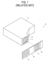
- FIG. 1 is a perspective view illustrating a conventional ink cartridge 10.
- the ink cartridge 10 comprises an ink storing part 11 which stores the ink, and a flexible printed circuit board (FPCB) 20, which is attached to the ink storing part 11 and exchanges an electrical signal with an image forming apparatus main body (not illustrated) through a contact pad 21.
- the FPCB 20 comprises a head chip 30 which discharges the ink of the ink storing part 11 onto the recording medium.
- the head chip 30 is attached to a head chip receiving hollow 13 of the ink cartridge 10.
- the head chip 30 is coupled with the head chip receiving hollow 13 by an adhesive.
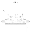
- FIGS. 2A and 2B are sectional views illustrating the ink cartridge 10 of FIG. 1.
- the head chip 30 comprises a substrate layer 32 having an ink supplying slit 31 which is supplied with the ink from an ink supplying hole 15 of the ink storing part 11, a chamber layer 34 having a heater 33 which heats the ink supplied from the ink supplying slit 31, and a nozzle layer 36 having a nozzle 35 where an ink bubble generated by heat from the heater 33 is used to discharge the ink to an outside.
- an adhesive A is applied onto a border surface to couple the head chip 30 with the ink storing part 11, and then the ink cartridge goes through a heat treatment at about 110°C. Therefore, the head chip 30 and the ink storing part 11 are solidly coupled therebetween.
- the ink storing part 11 of the conventional ink cartridge 10 is made of plastics and the substrate layer 32 of the head chip 30 is made of silicon, a shear stress F is generated on the border surface between the two materials which are of different kinds by a difference in coefficients of thermal expansion while the ink cartridge 10 goes through the heat treatment at about 110°C.
- a bending deformation ⁇ is generated in the substrate layer 32 as illustrated in FIG. 2B.
- the bending deformation of the substrate layer 32 causes a bending deformation of the nozzle layer 36, which is provided at an upper side of the substrate 32.
- the ink is discharged through the nozzle 35 obliquely instead of perpendicularly onto the recording medium, so that a printing quality is deteriorated.
- the nozzle layer 36 may be damaged due to the bending deformation of the nozzle layer 36.
- the problem caused by the bending deformation of the head chip 36 as described above may be more serious in a case of a line head, where the head chip 30 is provided in a number of parts.
- the present invention provides a head chip and ink cartridge having a reinforcing bridge to minimize deformation of the head chip when the head chip is coupled with an ink storing part, and an image forming apparatus having the same.
- a head chip usable in an image forming apparatus comprising a nozzle layer having a nozzle to discharge ink onto a recording medium, a substrate layer having at least one ink supplying slit provided to be parallel with the nozzle layer to supply the nozzle with the ink, and at least one reinforcing bridge provided along an extending direction of the ink supplying slit and blocks at least one region of the ink supplying slit.
- a thickness of the reinforcing bridge may not be greater than the thickness of the substrate layer.
- a width d of the reinforcing bridge may be p ⁇ 2 ⁇ d ⁇ p ⁇ 6 and p may be a pitch between adjacent nozzles.
- the reinforcing bridge may be provided plurally, or in a number of parts, along the extending direction of the ink supplying slit.
- the substrate layer may comprise a plurality of ink supplying slits which are provided to be parallel therewith.
- Each of the plurality of ink supplying slits may supply the nozzle with ink of a different color.
- a reinforcing bridge of a first ink supplying slit may be aligned with a reinforcing bridge of a neighboring ink supplying slit.
- a reinforcing bridge of a first ink supplying slit may not align with a reinforcing bridge of an adjacent ink supplying slit.
- an ink cartridge usable in an image forming apparatus comprising an ink storing part, and a head chip disposed at a lower side of the ink storing part to discharge ink onto a recording medium, the head chip comprising a nozzle layer having a nozzle to discharge ink onto a recording medium, a substrate layer having at least one ink supplying slit provided to be parallel with the nozzle layer and supplies the nozzle with the ink, and at least one reinforcing bridge provided along an extending direction of the ink supplying slit and blocks at least one region of the ink supplying slit.
- the ink storing part may be provided to correspond to a width of a printing medium and may comprise a plurality of head chips.
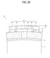
- FIG. 3A and FIG. 3B are a plan view and a sectional view, respectively, illustrating a substrate layer of a head chip according to an exemplary embodiment of the present general inventive concept.
- FIG. 4A is a sectional view illustrating the head chip of FIGS. 3A and 3B.
- an ink cartridge 100 may comprise an ink storing part 200 to store ink, and a head chip 300 which is provided at a lower side of the ink storing part 200 to discharge the ink from the ink storing part 200 onto a recording medium.
- the ink storing part 200 may comprise an ink chamber (not illustrated) in which the ink is stored, a foam chamber (not illustrated) to discharge the ink into the head chip 300 by a predetermined negative pressure, and a partitioning wall (not illustrated) to separate the ink chamber (not illustrated) from the foam chamber (not illustrated).
- a connecting opening part (not illustrated) may be provided at a lower end part of the partitioning wall (not illustrated) to allow the ink to flow from the ink chamber (not illustrated) to the foam chamber (not illustrated).
- a flexible printed circuit board (similar to FPCB 20 of FIG 1) can be combined to a lower part of the ink storing part 200 to exchange an electrical signal with an image forming part main body (not illustrated) through a contact pad (similar to contact pad 21 of FIG. 1).
- the ink storing part 200 may store ink of one color or ink of a plurality of colors. That is, the ink storing part 200 may comprise only a black ink storing part, or may comprise a plurality of ink storing parts 200 to correspond to each color of yellow, magenta, cyan, black and/or other known ink colors, respectively.
- the ink storing part 200 may be provided integrally with the head chip 300.
- the head chip 300 may also be provided on the image forming apparatus main body (not illustrated) and only the ink storing part 200 may be detachably provided.
- the head chip 300 may comprise a substrate layer 310 having an ink supplying slit 311 having a reinforcing bridge 313, a nozzle layer 330 having a nozzle 333 to discharge an ink droplet onto the recording medium, and a chamber layer 320 having an ink discharging device 321 to supply an energy to discharge the ink through the nozzle 333.
- the substrate layer 310 may comprise the ink supplying slit 311 which guides the ink in the ink storing part 200 to the nozzle layer 330, and the reinforcing bridge 313 which is provided in the ink supplying slit 311 to partially block an ink supply and to reinforce a strength of the substrate layer 310.
- the substrate layer 310 may be provided as a silicon wafer which is generally used in a manufacture of an integrated circuit.
- the ink supplying slit 311 is filled with the ink, which is supplied from the ink storing part 200, and supplies the ink to the chamber layer 320. As illustrated in FIG. 3A, the ink supplying slit 311 can be provided to have a predetermined length 1.
- the ink supplying slit 311 may be formed by etching a surface of a substrate 315 which is exposed through the nozzle 333. Alternatively, the ink supplying slit 311 may be formed by etching the surface of the substrate 315 prior to formation of the nozzle layer 330, or may be formed by etching a lower surface of the substrate 315 prior to coupling the substrate to the ink storing part 200.
- the ink supplying slit 311 may be provided as a single slit or may be provided plurally, or as a number of slits, as illustrated in FIG. 3A. If the ink supplying slit 311 is provided as a number of slits, each ink supplying slit 311 (311M, 311Y, 311C, and 311K in FIG. 3A) may supply ink of the same color or ink of different color with respect to the other ink supplying slits 311. For example, each ink supplying slit 311Y, 311M, 311C, and 311K may supply yellow, magenta, cyan, and black ink, respectively.
- the reinforcing bridge 313 is provided at the ink supplying slit 311 to prevent a bending deformation of the substrate layer 310, which may be generated when the head chip 300 is coupled with the ink storing part 200. As illustrated in FIG. 4A, the reinforcing bridge 313 may partially block the ink supplying slit 311 and reinforces the substrate layer 310 so that the substrate layer 310 may not be deformed by a shear stress F which may be generated by a difference in coefficients of thermal expansion between materials of the substrate 315 and the ink storing part 200. As a length of a part of the ink supplying slit 311 where the bending deformation may occur is decreased due to the reinforcing bridge 313, a maximum bending deformation amount may also be decreased.
- a thickness h1 of the reinforcing bridge 313 may be provided not to be greater than a thickness h of the substrate 315. That is, the thickness h1 of the reinforcing bridge 313 may be provided to be smaller than the thickness h of the substrate 315 as illustrated in FIG. 4A or a thickness h2 may be provided same as the thickness h of the substrate 315 as illustrated in FIG. 4B.
- the ink, which surrounds the reinforcing bridge 313, may be more easily supplied to the chamber layer 320 when the thickness h1 of the reinforcing bridge 313 is provided to be smaller than the thickness h of the substrate 315 than when the thickness h2 of the reinforcing bridge 313 is provided to be the same as the thickness h of the substrate 315.
- the thickness of the reinforcing bridge 313 may be provided properly by considering the ink supply to the nozzle 333 and the amount of the deformation of the substrate layer 310.
- a width d of the reinforcing bridge 313 may be provided not to obstruct the flow of the ink which is supplied to the nozzle 333.
- the width d of the reinforcing bridge 313 may be 2 to 6 times as large as a distance p between adjacent nozzles 333. If the width d of the reinforcing bridge 313 is smaller than twice the distance p, the ink may not be smoothly supplied to the nozzle 333 which surrounds the reinforcing bridge 313.
- the ink may not be smoothly supplied to the nozzle 333 which is disposed at a center of the plurality of the nozzles 333 surrounding the reinforcing bridge 313.
- the distance between adjacent reinforcing bridges 313 provided at the ink supplying slit 311 may be properly provided by considering a width w and the thickness h of the ink supplying slit 311.
- the reinforcing bridge 313 may be provided at each of the plurality of the ink supplying slits 311.
- the reinforcing bridges 313 may be provided in an alternating pattern so as to not align with a reinforcing bridge of an adjacent ink supplying slit 311.
- reinforcing bridge 313A of ink supplying slit 311Y is provided to alternate with reinforcing bridges 313 of the ink supplying slit 311M.
- the reinforcing bridges 313 may be provided to align with reinforcing bridges 313B which are provided at an adjacent ink supplying slit 311.
- the reinforcing bridge 313 may be formed by not etching a part of the substrate 315 to correspond to the thickness h1 and the width d of the reinforcing bridge 313 when the substrate 315 is etched to form the ink supplying slit 311.
- the reinforcing bridge 313 is provided integrally with the substrate 315.
- the reinforcing bridge 313 may be provided by attaching an additional member in the ink supplying slit 311 formed by etching.
- the chamber layer 320 may comprise the ink discharging device 321 which supplies the ink with the energy to discharge the ink through the nozzles 333, which is supplied through the ink supplying slit 311, onto the recording medium, and a chamber wall 323 which accommodates the ink discharging device 321.
- the ink discharging device 321 may be provided as a piezoelectric device or an electricity-heat transforming device, such as a heater.
- the chamber wall 323 can be made of epoxy resin. However, the chamber wall 323 may also be made of a photoresist resin of a silicon base, an acryl base, or an imide base.
- An electrode 340 can be provided at an outer side of the chamber layer 320 to apply a current to the ink discharging device 321.
- the electrode 340 may be made of aluminum or aluminum alloy which has a superior conductivity and may be easily patterned. Additionally, the electrode 340 can be provided as a layer formed over the ink discharging device 321 to supply a current thereto.
- the nozzle layer 330 may comprise the plurality of the nozzles 333 to discharge ink by the energy supplied by the ink discharging device 321 of the chamber layer 320.
- the nozzles 333 may be provided to be disposed in their maximum number per unit area.
- the ink which is supplied from the ink storing part 200 flows through the ink supplying slit 311 of the substrate layer 310 and into the chamber layer 320.
- the ink which fills the chamber layer 320 is discharged to the outside through the nozzle 333 by the energy supplied by the ink discharging device. For example, by an abrupt heating or vibration of the ink discharging device 321. That is, if the ink discharging device 321 is heated, an ink bubble is generated in the ink in the chamber layer 320. Then, the generated bubble pushes the ink via an expanding force of the bubble, so that the ink can be discharged through the nozzle 333.
- FIG. 6B illustrates an experimental result of an analysis through ANSYS on the deformation amount of the substrate layer 310 when the shear stress F of 20 [MPa] is applied to the head chip 300 of the ink cartridge 100 according to the present general inventive concept.
- the maximum deformation amount of the ink supplying slit 311 of the substrate layer 310 was 6.57 [ ⁇ m].
- the maximum deformation amount due to the same shear stress F was estimated to be 0.276 [ ⁇ m]. Therefore, it can be seen that a hardness of the head chip 300 according to the present general inventive concept is increased by about 24 times as much as that of the head chip lacking reinforcing bridges.
- the head chip according to embodiments of the present general inventive concept and the ink cartridge having the head chip comprise the plurality of the reinforcing bridges in the ink supplying slit, the bending deformation, which is generated when the ink storing part is combined with the head chip, can be minimized.
- the bending deformation of the head chip can be minimized by the reinforcing bridge, so that an ink discharging direction can be uniformly maintained, thus enhancing the printing quality.
- a surface of the nozzle can be maintained undamaged during a wiping process.
- the ink cartridge according to the exemplary embodiment of the present general inventive concept is a shuttle type ink cartridge which comprises only one head chip.
- the present general inventive concept is not limited thereto, and as illustrated in FIG. 7, the ink cartridge according to the present general inventive concept is applicable to a line head type ink cartridge with a width that corresponds to a width of the printing medium and comprising a plurality of the head chips.
- the head chip and the ink cartridge where the bending deformation of the substrate layer can be minimized, may be provided by having the reinforcing bridge in the ink supplying slit to reinforce the strength of the substrate layer.
Landscapes
- Physics & Mathematics (AREA)
- Thermal Sciences (AREA)
- Particle Formation And Scattering Control In Inkjet Printers (AREA)
- Ink Jet (AREA)
Abstract
Description
- The present invention relates to a head chip and ink cartridge and an image forming apparatus having the same, and more particularly, to a head chip and ink cartridge having an improved ink supplying slit structure and an image forming apparatus having the same.
- An image forming apparatus forms image data onto a recording medium according to a printing signal which is applied by a host. Generally, the image forming apparatus is divided into an inkjet type where an image is formed by discharging ink onto a recording medium, an electrophotographic type where the image is formed by selectively applying developer onto the recording medium using electric potential differences among a photosensitive member, the developer, and a transfer roller, and a thermal printing type where the image is formed by contacting an ink ribbon coated with ink with the recording medium and applying heat and pressure to transfer the ink to the recording medium.
- According to the inkjet type image forming apparatus, an ink cartridge in which the ink is stored discharges the ink onto the recording medium to form the image. The inkjet type image forming apparatus is divided into a shuttle type, where the ink cartridge discharges the ink while it shuttles in a direction perpendicular to a feeding direction of the recording medium, and a line head type, where the ink cartridge is provided to have a width to correspond to a width of the recording medium and forms the image by discharging the ink per whole width.
- FIG. 1 is a perspective view illustrating a
conventional ink cartridge 10. As illustrated in FIG. 1, theink cartridge 10 comprises anink storing part 11 which stores the ink, and a flexible printed circuit board (FPCB) 20, which is attached to theink storing part 11 and exchanges an electrical signal with an image forming apparatus main body (not illustrated) through acontact pad 21. The FPCB 20 comprises ahead chip 30 which discharges the ink of theink storing part 11 onto the recording medium. Thehead chip 30 is attached to a head chip receiving hollow 13 of theink cartridge 10. Thehead chip 30 is coupled with the head chip receiving hollow 13 by an adhesive. - FIGS. 2A and 2B are sectional views illustrating the
ink cartridge 10 of FIG. 1. Referring to FIGS. 2A and 2B, thehead chip 30 comprises asubstrate layer 32 having anink supplying slit 31 which is supplied with the ink from anink supplying hole 15 of theink storing part 11, achamber layer 34 having aheater 33 which heats the ink supplied from theink supplying slit 31, and anozzle layer 36 having anozzle 35 where an ink bubble generated by heat from theheater 33 is used to discharge the ink to an outside. - To manufacture the conventional ink cartridge having above structure, an adhesive A is applied onto a border surface to couple the
head chip 30 with theink storing part 11, and then the ink cartridge goes through a heat treatment at about 110°C. Therefore, thehead chip 30 and theink storing part 11 are solidly coupled therebetween. - However, since the
ink storing part 11 of theconventional ink cartridge 10 is made of plastics and thesubstrate layer 32 of thehead chip 30 is made of silicon, a shear stress F is generated on the border surface between the two materials which are of different kinds by a difference in coefficients of thermal expansion while theink cartridge 10 goes through the heat treatment at about 110°C. In particular, as the coefficient of thermal expansion of the plastics is 50 times greater than that of the silicon, a bending deformation δ is generated in thesubstrate layer 32 as illustrated in FIG. 2B. The bending deformation of thesubstrate layer 32 causes a bending deformation of thenozzle layer 36, which is provided at an upper side of thesubstrate 32. - If the deformation is generated in the
nozzle layer 36, the ink is discharged through thenozzle 35 obliquely instead of perpendicularly onto the recording medium, so that a printing quality is deteriorated. - Also, during a wiping process for removing foreign substances or ink which is attached to a surface of the nozzle, the
nozzle layer 36 may be damaged due to the bending deformation of thenozzle layer 36. - Moreover, the problem caused by the bending deformation of the
head chip 36 as described above may be more serious in a case of a line head, where thehead chip 30 is provided in a number of parts. - The present invention provides a head chip and ink cartridge having a reinforcing bridge to minimize deformation of the head chip when the head chip is coupled with an ink storing part, and an image forming apparatus having the same.
- Additional aspects and utilities of the present invention will be set forth in part in the description which follows and, in part, will be obvious from the description, or may be learned by practice of the present general inventive concept.
- According to the present invention there is provided an apparatus and method as set forth in the appended claims. Other features of the invention will be apparent from the dependent claims, and the description which follows.
- According to an aspect of the present invention there is provided a head chip usable in an image forming apparatus, the head chip comprising a nozzle layer having a nozzle to discharge ink onto a recording medium, a substrate layer having at least one ink supplying slit provided to be parallel with the nozzle layer to supply the nozzle with the ink, and at least one reinforcing bridge provided along an extending direction of the ink supplying slit and blocks at least one region of the ink supplying slit.
- A thickness of the reinforcing bridge may not be greater than the thickness of the substrate layer.
- A width d of the reinforcing bridge may be p×2 ≤ d ≤ p×6 and p may be a pitch between adjacent nozzles.
- The reinforcing bridge may be provided plurally, or in a number of parts, along the extending direction of the ink supplying slit.
- The substrate layer may comprise a plurality of ink supplying slits which are provided to be parallel therewith.
- Each of the plurality of ink supplying slits may supply the nozzle with ink of a different color.
- A reinforcing bridge of a first ink supplying slit may be aligned with a reinforcing bridge of a neighboring ink supplying slit.
- A reinforcing bridge of a first ink supplying slit may not align with a reinforcing bridge of an adjacent ink supplying slit.
- According to another aspect of the present invention there is provided an ink cartridge usable in an image forming apparatus, the ink cartridge comprising an ink storing part, and a head chip disposed at a lower side of the ink storing part to discharge ink onto a recording medium, the head chip comprising a nozzle layer having a nozzle to discharge ink onto a recording medium, a substrate layer having at least one ink supplying slit provided to be parallel with the nozzle layer and supplies the nozzle with the ink, and at least one reinforcing bridge provided along an extending direction of the ink supplying slit and blocks at least one region of the ink supplying slit.
- The ink storing part may be provided to correspond to a width of a printing medium and may comprise a plurality of head chips.
- These and/or other aspects and utilities of the present general inventive concept will become apparent and more readily appreciated from the following description of the embodiments, taken in conjunction with the accompanying drawings of which:
- FIG. 1 is an exploded perspective view illustrating a conventional ink cartridge;
- FIG. 2A and FIG. 2B are sectional views illustrating the conventional ink cartridge of FIG. 1 before deformation and after deformation, respectively;
- FIG. 3A and FIG. 3B illustrate a plan view and a sectional view, respectively, of a substrate layer of a head chip according to an exemplary embodiment of the present general inventive concept;
- FIG. 4A and FIG. 4B are sectional views illustrating the head chip according to the exemplary embodiment of the present general inventive concept;
- FIG. 5 is an expanded plan view illustrating a reinforcing bridge of the head chip according to an exemplary embodiment of the present general inventive concept;
- FIG. 6A and FIG. 6B illustrate experimental results about a strength of the head chip according to an exemplary embodiment of the present general inventive concept; and
- FIG. 7 is a plan view illustrating an ink cartridge according to an exemplary embodiment of the present general inventive concept.
- Reference will now be made in detail to the embodiments of the present general inventive concept, examples of which are illustrated in the accompanying drawings, wherein like reference numerals refer to like elements throughout. The embodiments are described below so as to explain the present general inventive concept by referring to the figures.
- FIG. 3A and FIG. 3B are a plan view and a sectional view, respectively, illustrating a substrate layer of a head chip according to an exemplary embodiment of the present general inventive concept. FIG. 4A is a sectional view illustrating the head chip of FIGS. 3A and 3B.
- As illustrated in FIG. 3A, FIG. 3B, and FIG. 4A, an
ink cartridge 100 according to the exemplary embodiment of the present general inventive concept may comprise anink storing part 200 to store ink, and ahead chip 300 which is provided at a lower side of theink storing part 200 to discharge the ink from theink storing part 200 onto a recording medium. - The
ink storing part 200 may comprise an ink chamber (not illustrated) in which the ink is stored, a foam chamber (not illustrated) to discharge the ink into thehead chip 300 by a predetermined negative pressure, and a partitioning wall (not illustrated) to separate the ink chamber (not illustrated) from the foam chamber (not illustrated). A connecting opening part (not illustrated) may be provided at a lower end part of the partitioning wall (not illustrated) to allow the ink to flow from the ink chamber (not illustrated) to the foam chamber (not illustrated). - A flexible printed circuit board (similar to
FPCB 20 of FIG 1) can be combined to a lower part of theink storing part 200 to exchange an electrical signal with an image forming part main body (not illustrated) through a contact pad (similar tocontact pad 21 of FIG. 1). Theink storing part 200 may store ink of one color or ink of a plurality of colors. That is, theink storing part 200 may comprise only a black ink storing part, or may comprise a plurality ofink storing parts 200 to correspond to each color of yellow, magenta, cyan, black and/or other known ink colors, respectively. - The
ink storing part 200 may be provided integrally with thehead chip 300. Alternatively, thehead chip 300 may also be provided on the image forming apparatus main body (not illustrated) and only theink storing part 200 may be detachably provided. - Since a structure of the
ink storing part 200 is similar to that illustrated in FIG. 1, a detailed description thereof is omitted. - As illustrated in FIG. 3A and FIG. 4A, the
head chip 300 may comprise asubstrate layer 310 having anink supplying slit 311 having a reinforcingbridge 313, anozzle layer 330 having anozzle 333 to discharge an ink droplet onto the recording medium, and achamber layer 320 having anink discharging device 321 to supply an energy to discharge the ink through thenozzle 333. - The
substrate layer 310 may comprise theink supplying slit 311 which guides the ink in theink storing part 200 to thenozzle layer 330, and the reinforcingbridge 313 which is provided in theink supplying slit 311 to partially block an ink supply and to reinforce a strength of thesubstrate layer 310. Thesubstrate layer 310 may be provided as a silicon wafer which is generally used in a manufacture of an integrated circuit. - The
ink supplying slit 311 is filled with the ink, which is supplied from theink storing part 200, and supplies the ink to thechamber layer 320. As illustrated in FIG. 3A, theink supplying slit 311 can be provided to have apredetermined length 1. Theink supplying slit 311 may be formed by etching a surface of asubstrate 315 which is exposed through thenozzle 333. Alternatively, theink supplying slit 311 may be formed by etching the surface of thesubstrate 315 prior to formation of thenozzle layer 330, or may be formed by etching a lower surface of thesubstrate 315 prior to coupling the substrate to theink storing part 200. - The
ink supplying slit 311 may be provided as a single slit or may be provided plurally, or as a number of slits, as illustrated in FIG. 3A. If theink supplying slit 311 is provided as a number of slits, each ink supplying slit 311 (311M, 311Y, 311C, and 311K in FIG. 3A) may supply ink of the same color or ink of different color with respect to the other ink supplying slits 311. For example, eachink supplying slit - The reinforcing
bridge 313 is provided at theink supplying slit 311 to prevent a bending deformation of thesubstrate layer 310, which may be generated when thehead chip 300 is coupled with theink storing part 200. As illustrated in FIG. 4A, the reinforcingbridge 313 may partially block theink supplying slit 311 and reinforces thesubstrate layer 310 so that thesubstrate layer 310 may not be deformed by a shear stress F which may be generated by a difference in coefficients of thermal expansion between materials of thesubstrate 315 and theink storing part 200. As a length of a part of theink supplying slit 311 where the bending deformation may occur is decreased due to the reinforcingbridge 313, a maximum bending deformation amount may also be decreased. - For example, a thickness h1 of the reinforcing
bridge 313 may be provided not to be greater than a thickness h of thesubstrate 315. That is, the thickness h1 of the reinforcingbridge 313 may be provided to be smaller than the thickness h of thesubstrate 315 as illustrated in FIG. 4A or a thickness h2 may be provided same as the thickness h of thesubstrate 315 as illustrated in FIG. 4B. The ink, which surrounds the reinforcingbridge 313, may be more easily supplied to thechamber layer 320 when the thickness h1 of the reinforcingbridge 313 is provided to be smaller than the thickness h of thesubstrate 315 than when the thickness h2 of the reinforcingbridge 313 is provided to be the same as the thickness h of thesubstrate 315. - However, the amount of the deformation which is generated if the
ink storing part 200 is combined with thehead chip 300 is small when the thickness h2 of the reinforcingbridge 313 is provided to be the same as the thickness h of thesubstrate 315. Therefore, the thickness of the reinforcingbridge 313 may be provided properly by considering the ink supply to thenozzle 333 and the amount of the deformation of thesubstrate layer 310. - On the other hand, a width d of the reinforcing
bridge 313 may be provided not to obstruct the flow of the ink which is supplied to thenozzle 333. Experimentally, as illustrated in FIG. 5, the width d of the reinforcingbridge 313 may be 2 to 6 times as large as a distance p betweenadjacent nozzles 333. If the width d of the reinforcingbridge 313 is smaller than twice the distance p, the ink may not be smoothly supplied to thenozzle 333 which surrounds the reinforcingbridge 313. Also, if the width d of the reinforcingbridge 313 is larger than six times the distance p, the ink may not be smoothly supplied to thenozzle 333 which is disposed at a center of the plurality of thenozzles 333 surrounding the reinforcingbridge 313. - Also, if a distance between adjacent reinforcing
bridges 313 provided at theink supplying slit 311 is small, deformation of the substrate layer can be reduced. However, the small distance between adjacent reinforcingbridges 313 may be an influence upon the smooth supply of the ink. Therefore, the distance between adjacent reinforcingbridges 313 may be properly provided by considering a width w and the thickness h of theink supplying slit 311. - The reinforcing
bridge 313 may be provided at each of the plurality of the ink supplying slits 311. In this case, as illustrated in FIG. 3A, the reinforcingbridges 313 may be provided in an alternating pattern so as to not align with a reinforcing bridge of an adjacentink supplying slit 311. For example, as illustrated in FIG. 3A, reinforcing bridge 313A ofink supplying slit 311Y is provided to alternate with reinforcingbridges 313 of theink supplying slit 311M. Alternatively, as illustrated in FIG. 6A, the reinforcingbridges 313 may be provided to align with reinforcingbridges 313B which are provided at an adjacentink supplying slit 311. - The reinforcing
bridge 313 may be formed by not etching a part of thesubstrate 315 to correspond to the thickness h1 and the width d of the reinforcingbridge 313 when thesubstrate 315 is etched to form theink supplying slit 311. In this case, the reinforcingbridge 313 is provided integrally with thesubstrate 315. Alternatively, the reinforcingbridge 313 may be provided by attaching an additional member in theink supplying slit 311 formed by etching. - The
chamber layer 320 may comprise theink discharging device 321 which supplies the ink with the energy to discharge the ink through thenozzles 333, which is supplied through theink supplying slit 311, onto the recording medium, and achamber wall 323 which accommodates theink discharging device 321. In this case, theink discharging device 321 may be provided as a piezoelectric device or an electricity-heat transforming device, such as a heater. Thechamber wall 323 can be made of epoxy resin. However, thechamber wall 323 may also be made of a photoresist resin of a silicon base, an acryl base, or an imide base. - An
electrode 340 can be provided at an outer side of thechamber layer 320 to apply a current to theink discharging device 321. Theelectrode 340 may be made of aluminum or aluminum alloy which has a superior conductivity and may be easily patterned. Additionally, theelectrode 340 can be provided as a layer formed over theink discharging device 321 to supply a current thereto. - The
nozzle layer 330 may comprise the plurality of thenozzles 333 to discharge ink by the energy supplied by theink discharging device 321 of thechamber layer 320. In this case, themore nozzles 333 that are provided, the more a printing quality is improved. Therefore, thenozzles 333 may be provided to be disposed in their maximum number per unit area. - Hereinafter, an operating process of the
ink cartridge 100 according to the present general inventive concept is described. First, the ink which is supplied from theink storing part 200 flows through theink supplying slit 311 of thesubstrate layer 310 and into thechamber layer 320. The ink which fills thechamber layer 320 is discharged to the outside through thenozzle 333 by the energy supplied by the ink discharging device. For example, by an abrupt heating or vibration of theink discharging device 321. That is, if theink discharging device 321 is heated, an ink bubble is generated in the ink in thechamber layer 320. Then, the generated bubble pushes the ink via an expanding force of the bubble, so that the ink can be discharged through thenozzle 333. - FIG. 6B illustrates an experimental result of an analysis through ANSYS on the deformation amount of the
substrate layer 310 when the shear stress F of 20 [MPa] is applied to thehead chip 300 of theink cartridge 100 according to the present general inventive concept. - According to the experimental result, when there is no reinforcing bridges, the maximum deformation amount of the
ink supplying slit 311 of thesubstrate layer 310 was 6.57 [µm]. On the other hand, as illustrated in FIG. 6A, in thehead chip 300 according to the present general inventive concept having five reinforcingbridges 313 each with a respective width of 84 [µm] for eachink supplying slit 311, the maximum deformation amount due to the same shear stress F was estimated to be 0.276 [µm]. Therefore, it can be seen that a hardness of thehead chip 300 according to the present general inventive concept is increased by about 24 times as much as that of the head chip lacking reinforcing bridges. - As described above, as the head chip according to embodiments of the present general inventive concept and the ink cartridge having the head chip comprise the plurality of the reinforcing bridges in the ink supplying slit, the bending deformation, which is generated when the ink storing part is combined with the head chip, can be minimized.
- Also, as described above, the bending deformation of the head chip can be minimized by the reinforcing bridge, so that an ink discharging direction can be uniformly maintained, thus enhancing the printing quality.
- Also, as a degree of the bending deformation is small, a surface of the nozzle can be maintained undamaged during a wiping process.
- In the above description, the ink cartridge according to the exemplary embodiment of the present general inventive concept is a shuttle type ink cartridge which comprises only one head chip. However, the present general inventive concept is not limited thereto, and as illustrated in FIG. 7, the ink cartridge according to the present general inventive concept is applicable to a line head type ink cartridge with a width that corresponds to a width of the printing medium and comprising a plurality of the head chips.
- As described above, according to the present general inventive concept, the head chip and the ink cartridge, where the bending deformation of the substrate layer can be minimized, may be provided by having the reinforcing bridge in the ink supplying slit to reinforce the strength of the substrate layer.
- Although a few exemplary embodiments of the present general inventive concept have been shown and described, it will be appreciated by those skilled in the art that changes may be made in these embodiments without departing from the principles of the general inventive concept, the scope of which is defined in the appended claims and their equivalents.
- Attention is directed to all papers and documents which are filed concurrently with or previous to this specification in connection with this application and which are open to public inspection with this specification, and the contents of all such papers and documents are incorporated herein by reference.
- All of the features disclosed in this specification (including any accompanying claims, abstract and drawings), and/or all of the steps of any method or process so disclosed, may be combined in any combination, except combinations where at least some of such features and/or steps are mutually exclusive.
- Each feature disclosed in this specification (including any accompanying claims, abstract and drawings) may be replaced by alternative features serving the same, equivalent or similar purpose, unless expressly stated otherwise. Thus, unless expressly stated otherwise, each feature disclosed is one example only of a generic series of equivalent or similar features.
- The invention is not restricted to the details of the foregoing embodiment(s). The invention extends to any novel one, or any novel combination, of the features disclosed in this specification (including any accompanying claims, abstract and drawings), or to any novel one, or any novel combination, of the steps of any method or process so disclosed.
Claims (17)
- A head chip usable in an image forming apparatus, the head chip comprising:a nozzle layer (330) having a nozzle (333) to discharge ink onto a recording medium;a substrate layer (310) having at least one ink supplying slit (311) provided to be parallel with the nozzle layer (330) to supply the nozzle (333) with the ink; andat least one reinforcing bridge provided along an extending direction of the ink supplying slit (311) and blocks at least one region of the ink supplying slit (311).
- The head chip of claim 1, wherein a thickness of the reinforcing bridge (313) is not greater than the thickness of the substrate layer (310).
- The head chip of claim 1 or 2, wherein a width d of the reinforcing bridge (313) is p×2 ≤ d ≤ p×6 and p is a pitch between adjacent nozzles.
- The head chip of any preceding claim, wherein the reinforcing bridge (313) is provided in a number of parts along the extending direction of the ink supplying slit (311).
- The head chip of any preceding claim, wherein the substrate layer (310) comprises a plurality of ink supplying slits which are provided to be parallel therewith.
- The head chip of claim 5, wherein each of the plurality of ink supplying slits supplies the nozzle (333) with ink of a different color.
- The head chip of claim 5 or claim 6, wherein a reinforcing bridge (313) of a first ink supplying slit (311) is aligned with a reinforcing bridge (313) of a neighboring ink supplying slit (311).
- The head chip of claim 5, wherein a reinforcing bridge (313) of a first ink supplying slit (311) does not align with a reinforcing bridge (313) of an adjacent ink supplying slit (311).
- An ink cartridge usable in an image forming apparatus, the ink cartridge comprising:an ink storing part (200); anda head chip (300) disposed at a lower side of the ink storing part (200) to discharge ink onto a recording medium, the head chip (300) comprising:a nozzle layer (330) having a nozzle (333) to discharge ink onto a recording medium;a substrate layer (310) having at least one ink supplying slit (311) provided to be parallel with the nozzle layer (330) and supplies the nozzle (333) with the ink; andat least one reinforcing bridge (313) provided along an extending direction of the ink supplying slit (311) and blocks at least one region of the ink supplying slit (311).
- The ink cartridge of claim 9, wherein the ink storing part (200) is provided to correspond to a width of a printing medium and comprises a plurality of head chips.
- The ink cartridge of claim 9 or claim 10, wherein a thickness of the reinforcing bridge (313) is not greater than the thickness of the substrate layer (310).
- The ink cartridge of claim 9 or 11, wherein a width d of the reinforcing bridge (313) is p×2 ≤ d ≤ p×6 and p is a pitch between adjacent nozzles.
- The ink cartridge of any one of claims 9 to 12, wherein the reinforcing bridge (313) is provided in a number of parts along the extending direction of the ink supplying slit (311).
- The ink cartridge of any one of claims 9 to 13, wherein the substrate layer (310) comprises a plurality of ink supplying slits which are provided to be parallel therewith.
- The ink cartridge of any one of claims 9 to 14, wherein each of the plurality of ink supplying slits supplies the nozzle (333) with ink of a different color.
- The ink cartridge of any one of claims 9 to 15 wherein a reinforcing bridge (313) of a first ink supplying slit (311) is aligned with a reinforcing bridge (313) of a neighboring ink supplying slit (311).
- The ink cartridge of any one of claims 9 to 15, wherein the reinforcing bridge (313) of a first ink supplying slit (311) does not align with a reinforcing bridge (313) of an adjacent ink supplying slit (311).
Applications Claiming Priority (1)
| Application Number | Priority Date | Filing Date | Title |
|---|---|---|---|
| KR1020060116463A KR20080046865A (en) | 2006-11-23 | 2006-11-23 | Head chip and ink cartridge for image forming apparatus including the same |
Publications (2)
| Publication Number | Publication Date |
|---|---|
| EP1925449A2 true EP1925449A2 (en) | 2008-05-28 |
| EP1925449A3 EP1925449A3 (en) | 2009-05-06 |
Family
ID=39190349
Family Applications (1)
| Application Number | Title | Priority Date | Filing Date |
|---|---|---|---|
| EP07121131A Withdrawn EP1925449A3 (en) | 2006-11-23 | 2007-11-20 | Head chip and ink cartridge and image forming apparatus having the same |
Country Status (4)
| Country | Link |
|---|---|
| US (1) | US20080122894A1 (en) |
| EP (1) | EP1925449A3 (en) |
| KR (1) | KR20080046865A (en) |
| CN (1) | CN101186149A (en) |
Families Citing this family (9)
| Publication number | Priority date | Publication date | Assignee | Title |
|---|---|---|---|---|
| CN103625111B (en) * | 2012-08-27 | 2016-09-28 | 研能科技股份有限公司 | Page Wide Inkjet Printing Device |
| US9647997B2 (en) | 2013-03-13 | 2017-05-09 | Nagrastar, Llc | USB interface for performing transport I/O |
| USD758372S1 (en) * | 2013-03-13 | 2016-06-07 | Nagrastar Llc | Smart card interface |
| USD759022S1 (en) | 2013-03-13 | 2016-06-14 | Nagrastar Llc | Smart card interface |
| US9888283B2 (en) | 2013-03-13 | 2018-02-06 | Nagrastar Llc | Systems and methods for performing transport I/O |
| USD729808S1 (en) | 2013-03-13 | 2015-05-19 | Nagrastar Llc | Smart card interface |
| USD780763S1 (en) | 2015-03-20 | 2017-03-07 | Nagrastar Llc | Smart card interface |
| USD864968S1 (en) | 2015-04-30 | 2019-10-29 | Echostar Technologies L.L.C. | Smart card interface |
| JP6905786B2 (en) * | 2017-09-28 | 2021-07-21 | 京セラ株式会社 | Flow path member, liquid discharge head and recording device |
Family Cites Families (9)
| Publication number | Priority date | Publication date | Assignee | Title |
|---|---|---|---|---|
| US5469199A (en) * | 1990-08-16 | 1995-11-21 | Hewlett-Packard Company | Wide inkjet printhead |
| US5537133A (en) * | 1992-04-02 | 1996-07-16 | Hewlett-Packard Company | Restraining element for a print cartridge body to reduce thermally induced stress |
| US6557983B1 (en) * | 1995-08-30 | 2003-05-06 | Canon Kabushiki Kaisha | Ink jet head, substrate for ink jet head, ink jet cartridge, and ink jet apparatus |
| US6398348B1 (en) * | 2000-09-05 | 2002-06-04 | Hewlett-Packard Company | Printing structure with insulator layer |
| US6419346B1 (en) * | 2001-01-25 | 2002-07-16 | Hewlett-Packard Company | Two-step trench etch for a fully integrated thermal inkjet printhead |
| US6679587B2 (en) * | 2001-10-31 | 2004-01-20 | Hewlett-Packard Development Company, L.P. | Fluid ejection device with a composite substrate |
| US6672712B1 (en) * | 2002-10-31 | 2004-01-06 | Hewlett-Packard Development Company, L.P. | Slotted substrates and methods and systems for forming same |
| JP4522086B2 (en) * | 2003-12-15 | 2010-08-11 | キヤノン株式会社 | Beam, beam manufacturing method, ink jet recording head including beam, and ink jet recording head manufacturing method |
| US7469989B2 (en) * | 2004-01-21 | 2008-12-30 | Silverbrook Research Pty Ltd | Printhead chip having longitudinal ink supply channels interrupted by transverse bridges |
-
2006
- 2006-11-23 KR KR1020060116463A patent/KR20080046865A/en not_active Application Discontinuation
-
2007
- 2007-06-25 US US11/767,718 patent/US20080122894A1/en not_active Abandoned
- 2007-11-19 CN CNA2007101878333A patent/CN101186149A/en active Pending
- 2007-11-20 EP EP07121131A patent/EP1925449A3/en not_active Withdrawn
Non-Patent Citations (1)
| Title |
|---|
| None |
Also Published As
| Publication number | Publication date |
|---|---|
| CN101186149A (en) | 2008-05-28 |
| KR20080046865A (en) | 2008-05-28 |
| US20080122894A1 (en) | 2008-05-29 |
| EP1925449A3 (en) | 2009-05-06 |
Similar Documents
| Publication | Publication Date | Title |
|---|---|---|
| EP1925449A2 (en) | Head chip and ink cartridge and image forming apparatus having the same | |
| US6910759B2 (en) | Liquid discharge recording head cartridge and liquid discharge recording apparatus | |
| AU785434B2 (en) | Liquid discharge recording head, liquid discharge recording apparatus, and method for manufacturing liquid discharge head | |
| KR20100060276A (en) | Nozzle plate and method of manufacturing the same | |
| US10029466B2 (en) | Ink-jet recording head, recording element substrate, method for manufacturing ink-jet recording head, and method for manufacturing recording element substrate | |
| EP1733883B1 (en) | Liquid discharge head and recording device | |
| ITAO990002A1 (en) | MULTIPLE CHANNEL HEAD OF INK FEED | |
| US7905573B2 (en) | Liquid ejection head with nozzle plate deformed by heat and image forming apparatus including the liquid election head | |
| AU660746B2 (en) | Ink jet recording head, ink jet recording head cartridge and recording apparatus using same | |
| JP3679740B2 (en) | Ink jet recording head and ink jet recording apparatus | |
| US20080049073A1 (en) | Inkjet printhead and method of manufacturing the same | |
| EP1893410B1 (en) | Nozzle plate for an ink jet print head comprising stress relieving elements | |
| EP2008824B1 (en) | Head chip usable with inkjet image forming apparatus and manufacturing method of the same | |
| EP0894628A2 (en) | Liquid discharging method, liquid discharging head, and head cartridge and liquid discharging apparatus using said liquid discharging head | |
| JPH10138474A (en) | Ink jet head | |
| JP7143666B2 (en) | Head unit and inkjet recording device | |
| JP4417240B2 (en) | Method for manufacturing printer device | |
| JP2006130766A (en) | Substrate for liquid delivering head and its manufacturing method | |
| JP2007021909A (en) | Liquid delivery head and liquid delivery apparatus | |
| JP2008012753A (en) | Liquid droplet ejecting head, its manufacturing method and liquid droplet ejector | |
| EP1604824A1 (en) | Liquid-jet head and liquid-jet device using the head | |
| JP2006335069A (en) | Array head bonding structure for ink cartridge and method of bonding array head structure for ink cartridge | |
| JPH09156096A (en) | Inkjet printer | |
| TWI495570B (en) | Inkjet printhead assembly having backside electrical connection | |
| JP2001301176A (en) | Method for joining substrate, method for manufacturing substrate, and method for manufacturing recording head and nozzle substrate |
Legal Events
| Date | Code | Title | Description |
|---|---|---|---|
| PUAI | Public reference made under article 153(3) epc to a published international application that has entered the european phase |
Free format text: ORIGINAL CODE: 0009012 |
|
| AK | Designated contracting states |
Kind code of ref document: A2 Designated state(s): AT BE BG CH CY CZ DE DK EE ES FI FR GB GR HU IE IS IT LI LT LU LV MC MT NL PL PT RO SE SI SK TR |
|
| AX | Request for extension of the european patent |
Extension state: AL BA HR MK RS |
|
| PUAL | Search report despatched |
Free format text: ORIGINAL CODE: 0009013 |
|
| AK | Designated contracting states |
Kind code of ref document: A3 Designated state(s): AT BE BG CH CY CZ DE DK EE ES FI FR GB GR HU IE IS IT LI LT LU LV MC MT NL PL PT RO SE SI SK TR |
|
| AX | Request for extension of the european patent |
Extension state: AL BA HR MK RS |
|
| 17P | Request for examination filed |
Effective date: 20091106 |
|
| 17Q | First examination report despatched |
Effective date: 20091201 |
|
| AKX | Designation fees paid |
Designated state(s): DE FR GB NL |
|
| GRAP | Despatch of communication of intention to grant a patent |
Free format text: ORIGINAL CODE: EPIDOSNIGR1 |
|
| STAA | Information on the status of an ep patent application or granted ep patent |
Free format text: STATUS: THE APPLICATION IS DEEMED TO BE WITHDRAWN |
|
| 18D | Application deemed to be withdrawn |
Effective date: 20120113 |