EP1921643A2 - Pressure contact array - Google Patents
Pressure contact array Download PDFInfo
- Publication number
- EP1921643A2 EP1921643A2 EP07018492A EP07018492A EP1921643A2 EP 1921643 A2 EP1921643 A2 EP 1921643A2 EP 07018492 A EP07018492 A EP 07018492A EP 07018492 A EP07018492 A EP 07018492A EP 1921643 A2 EP1921643 A2 EP 1921643A2
- Authority
- EP
- European Patent Office
- Prior art keywords
- pad
- terminal contact
- contact arrangement
- pad elements
- circuit board
- Prior art date
- Legal status (The legal status is an assumption and is not a legal conclusion. Google has not performed a legal analysis and makes no representation as to the accuracy of the status listed.)
- Granted
Links
Images


Classifications
-
- H—ELECTRICITY
- H05—ELECTRIC TECHNIQUES NOT OTHERWISE PROVIDED FOR
- H05K—PRINTED CIRCUITS; CASINGS OR CONSTRUCTIONAL DETAILS OF ELECTRIC APPARATUS; MANUFACTURE OF ASSEMBLAGES OF ELECTRICAL COMPONENTS
- H05K3/00—Apparatus or processes for manufacturing printed circuits
- H05K3/40—Forming printed elements for providing electric connections to or between printed circuits
- H05K3/4007—Surface contacts, e.g. bumps
- H05K3/4015—Surface contacts, e.g. bumps using auxiliary conductive elements, e.g. pieces of metal foil, metallic spheres
-
- H—ELECTRICITY
- H01—ELECTRIC ELEMENTS
- H01R—ELECTRICALLY-CONDUCTIVE CONNECTIONS; STRUCTURAL ASSOCIATIONS OF A PLURALITY OF MUTUALLY-INSULATED ELECTRICAL CONNECTING ELEMENTS; COUPLING DEVICES; CURRENT COLLECTORS
- H01R12/00—Structural associations of a plurality of mutually-insulated electrical connecting elements, specially adapted for printed circuits, e.g. printed circuit boards [PCB], flat or ribbon cables, or like generally planar structures, e.g. terminal strips, terminal blocks; Coupling devices specially adapted for printed circuits, flat or ribbon cables, or like generally planar structures; Terminals specially adapted for contact with, or insertion into, printed circuits, flat or ribbon cables, or like generally planar structures
- H01R12/50—Fixed connections
- H01R12/51—Fixed connections for rigid printed circuits or like structures
- H01R12/55—Fixed connections for rigid printed circuits or like structures characterised by the terminals
- H01R12/57—Fixed connections for rigid printed circuits or like structures characterised by the terminals surface mounting terminals
-
- H—ELECTRICITY
- H01—ELECTRIC ELEMENTS
- H01R—ELECTRICALLY-CONDUCTIVE CONNECTIONS; STRUCTURAL ASSOCIATIONS OF A PLURALITY OF MUTUALLY-INSULATED ELECTRICAL CONNECTING ELEMENTS; COUPLING DEVICES; CURRENT COLLECTORS
- H01R43/00—Apparatus or processes specially adapted for manufacturing, assembling, maintaining, or repairing of line connectors or current collectors or for joining electric conductors
- H01R43/16—Apparatus or processes specially adapted for manufacturing, assembling, maintaining, or repairing of line connectors or current collectors or for joining electric conductors for manufacturing contact members, e.g. by punching and by bending
-
- H—ELECTRICITY
- H01—ELECTRIC ELEMENTS
- H01H—ELECTRIC SWITCHES; RELAYS; SELECTORS; EMERGENCY PROTECTIVE DEVICES
- H01H13/00—Switches having rectilinearly-movable operating part or parts adapted for pushing or pulling in one direction only, e.g. push-button switch
- H01H13/70—Switches having rectilinearly-movable operating part or parts adapted for pushing or pulling in one direction only, e.g. push-button switch having a plurality of operating members associated with different sets of contacts, e.g. keyboard
- H01H13/81—Switches having rectilinearly-movable operating part or parts adapted for pushing or pulling in one direction only, e.g. push-button switch having a plurality of operating members associated with different sets of contacts, e.g. keyboard characterised by electrical connections to external devices
-
- H—ELECTRICITY
- H05—ELECTRIC TECHNIQUES NOT OTHERWISE PROVIDED FOR
- H05K—PRINTED CIRCUITS; CASINGS OR CONSTRUCTIONAL DETAILS OF ELECTRIC APPARATUS; MANUFACTURE OF ASSEMBLAGES OF ELECTRICAL COMPONENTS
- H05K1/00—Printed circuits
- H05K1/02—Details
- H05K1/11—Printed elements for providing electric connections to or between printed circuits
-
- H—ELECTRICITY
- H05—ELECTRIC TECHNIQUES NOT OTHERWISE PROVIDED FOR
- H05K—PRINTED CIRCUITS; CASINGS OR CONSTRUCTIONAL DETAILS OF ELECTRIC APPARATUS; MANUFACTURE OF ASSEMBLAGES OF ELECTRICAL COMPONENTS
- H05K2201/00—Indexing scheme relating to printed circuits covered by H05K1/00
- H05K2201/10—Details of components or other objects attached to or integrated in a printed circuit board
- H05K2201/10007—Types of components
- H05K2201/10053—Switch
-
- H—ELECTRICITY
- H05—ELECTRIC TECHNIQUES NOT OTHERWISE PROVIDED FOR
- H05K—PRINTED CIRCUITS; CASINGS OR CONSTRUCTIONAL DETAILS OF ELECTRIC APPARATUS; MANUFACTURE OF ASSEMBLAGES OF ELECTRICAL COMPONENTS
- H05K2203/00—Indexing scheme relating to apparatus or processes for manufacturing printed circuits covered by H05K3/00
- H05K2203/03—Metal processing
- H05K2203/033—Punching metal foil, e.g. solder foil
-
- H—ELECTRICITY
- H05—ELECTRIC TECHNIQUES NOT OTHERWISE PROVIDED FOR
- H05K—PRINTED CIRCUITS; CASINGS OR CONSTRUCTIONAL DETAILS OF ELECTRIC APPARATUS; MANUFACTURE OF ASSEMBLAGES OF ELECTRICAL COMPONENTS
- H05K3/00—Apparatus or processes for manufacturing printed circuits
- H05K3/30—Assembling printed circuits with electric components, e.g. with resistor
- H05K3/32—Assembling printed circuits with electric components, e.g. with resistor electrically connecting electric components or wires to printed circuits
- H05K3/34—Assembling printed circuits with electric components, e.g. with resistor electrically connecting electric components or wires to printed circuits by soldering
- H05K3/341—Surface mounted components
Definitions
- the invention relates in particular to a contact-contact array or a AnpressCAMan angel, in particular SMD-solderable.
- the invention further relates to a method for attaching AnpressCAMen to a circuit board and in particular by means of a AnpressCAMan nie.
- the invention relates generally to a terminal contact arrangement.
- Printed circuit boards have contact surfaces, in particular for connection purposes, on which, for example, components can be soldered. These contact surfaces are often referred to as pad surfaces or shortly as pads. Hereinafter, these pads, after being on the circuit board, will be referred to as board pads.
- the positioning is made with respect to the circuit board pads and then initiated the soldering process. Because the pad elements fastened to the pilot strip are fixed to one another or to one another, they do not lose their exact positioning.
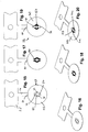
- Fig. 1 is a schematic plan view of a surface of a circuit board 10, on which circuit board pads 11 are formed, for example, have a circular surface shape.
- an annular printed circuit board pad 12 is shown, which surrounds a circular printed circuit board pad 13 spaced.
- segmental printed circuit board pads 14, 15, 16 and 17 are shown. Conductor tracks are designated by 18.
- pad elements 140, 150, 160, 170 may be referred to as pad elements 140, 150, 160, 170.
- FIG. 3 shows a pilot strip 25 to which four pad elements 141, 151, 161, 171 of the pressing contact arrangement 21 are fastened by means of a web 26.
- FIGS. 3 and 4 illustrate a first manufacturing stage of the solderable contact pressing arrangement 21 shown in FIGS. 7 and 8. A plurality of such contact contact arrangements 21 may be arranged at a distance from the pilot strip 25. The individual pad elements 141, 151, 161, 171 are separated by punched slots 28 and connected in this first production stage by a circular disk 27.
- a molding material 130 is introduced into the slots 28.
- the molding material 130 preferably connects the pad elements 141, 151, 161, 171 to one another at the edges.
- the pad elements 141, 151, 161, 171 form, after in a third Endstanzgrin punching out of a hole 29 leaving disc 27 (an unnecessary connecting part), a unit.
- the finished Anpressromean angel 21 shown in Fig. 7 and 8 can then be easily aligned with the PCB contact pads 14, 15, 16, 17 and soldered. After soldering takes place in a further step, the separation of the web 26, preferably along a predetermined breaking point or predetermined breaking line.
- non-segment-shaped pad elements are formed, but square pad elements 142, 152, 162 and 172. These are shown in FIGS. 9 and 10 separated by slots 30, but centrally with a cross-shaped Disc 31 connected, which - as seen in Fig. 13 - leaves after punching out a cross-shaped hole 32.
- Two webs 26 each connect the pad elements 162, 172 to the pilot strip 25, predetermined breaking points 60 are, as shown, provided.
- a molding material 130 is injected into the slots 30 before punching out the disk 31, and thus the pad members 142, 152, 162, 172 are connected to each other and remain connected even after the cross-shaped disk 31 is punched out.
- the pressing contact assembly 22 thus formed is placed and soldered on respective circuit board pads.
- the Anpresstitlean angel (generally: terminal contact arrangement) 23, a first pad member 143 in the form of an annular contact disc and a second pad member 153 in the Shape of a contact plate on.
- two slits 34 and 35 are punched in a circular, preferably made of metal disc 33 in mirror image. These slots 34, 35 form the contour for the second or inner pad member 153, i. a first pressing contact in the form of a circular plate. However, according to FIG. 15, this second pad element 153 (pressing contact) is still connected by connecting webs 36, 37 to the first, outer annular pad element 143 (pressing contact).
- the slots 34, 35 are filled with molding material 130 and subsequently in a third method step, two circular disks (non-required connecting parts) are punched out, whose diameter holes 38 and 39 according to FIGS. 19 and 20 equivalent.
- the first and second pad elements 143, 153 are electrically isolated but mechanically connected:
- the inner pad element 153 is galvanically separated from the outer pad element 143, but remains mechanically connected to one another by means of the molding compound 200, 201 with the aid of the molding material 130.
- predetermined breaking points 60 are provided in the joints (i.e., lands 26) between the pilot strips 25 and at least one of the pad members 171; 162; 172; 253 predetermined breaking points 60 are provided.
- the invention relates in particular to an arrangement of pressing contacts, wherein the pressing contacts are formed by so-called pad elements which, when it comes to pressing contacts, have pressing contact zones in which the contact pressure takes place.
- terminal contacts can also be provided in terminal contact arrangements in order to be soldered to printed circuit board pads as long as they still form a unit.
- the pad elements are used as pressing contacts, then it may be expedient to provide a galvanic coating in the Anpress1:00zonen the pad elements.
- the pad elements forming a terminal contact or pressing contact arrangement are preferably connected to one another in a coplanar plane.
- the pad elements forming a terminal contact or AnpressANDan angel are punched from a surface element, such as a metal sheet, wherein preferably slots or recesses delimit the pad elements from each other. After punching out the recesses forming sheet metal or surface element parts, the slots or recesses formed are completely or partially filled by the molding material 130, which produces a stable mechanical connection between the different pad elements, but also the pad elements electrically insulated from each other.
Abstract
Description
Die Erfindung bezieht sich insbesondere auf eine Anpress-Kontakt-Array bzw. eine Anpresskontaktanordnung, die insbesondere SMD-lötbar ist. Die Erfindung bezieht sich ferner auf ein Verfahren zur Anbringung von Anpresskontakten an einer Leiterplatte und zwar insbesondere mittels einer Anpresskontaktanordnung. Die Erfindung bezieht sich allgemein auf eine Anschlusskontaktanordnung.The invention relates in particular to a contact-contact array or a Anpresskontaktanordnung, in particular SMD-solderable. The invention further relates to a method for attaching Anpresskontakten to a circuit board and in particular by means of a Anpresskontaktanordnung. The invention relates generally to a terminal contact arrangement.
Leiterplatten besitzen insbesondere zu Anschlusszwecken Kontaktflächen, an denen beispielsweise Bauteile angelötet werden können. Diese Kontaktflächen werden häufig auch als Pad-Flächen oder kurz als Pads bezeichnet. Im Folgenden werden diese Pads, nachdem sie sich auf der Leiterplatte befinden, als Leiterplatten-Pads bezeichnet.Printed circuit boards have contact surfaces, in particular for connection purposes, on which, for example, components can be soldered. These contact surfaces are often referred to as pad surfaces or shortly as pads. Hereinafter, these pads, after being on the circuit board, will be referred to as board pads.
Es ist häufig erforderlich, an den Leiterplatten-Pads, Bauteile, insbesondere Kontaktpads oder Pad-Elemente anzulöten. Wenn diese Pad-Elemente mit Anpresskontaktzonen versehen sind, so können die Pad-Elemente zum Kontaktieren von z.B. Anpresskontakten für den Anschluss von z.B. Lautsprechern oder Tastaturen dienen, wobei die Pad-Elemente als Anpresskontakte oder Anpresskontaktelemente bezeichnet werden. Ein Lautsprecher oder eine Tastatur würde dann beispielsweise Anpresskontakte aufweisen, z.B. Löffelkontakte, die auf die Anpresskontaktzonen der Pad-Elemente drücken. Diese Anpresskontakte bzw. Anpresskontaktelemente können beispielsweise aus Gold bestehen, um a) die Kontaktsicherheit zu erhöhen und b) die oftmals notwendigen niedrigen Übergangswiderstände zu erreichen.It is often necessary to solder components, in particular contact pads or pad elements, to the circuit board pads. If these pad elements are provided with contact areas, the pad elements can be used to contact e.g. Pressing contacts for the connection of e.g. Serve speakers or keyboards, the pad elements are referred to as Anpresskontakte or Anpresskontaktelemente. A loudspeaker or keyboard would then have, for example contact contacts, e.g. Spoon contacts that press on the contact areas of the pad elements. These Anpresskontakte or Anpresskontaktelemente may for example consist of gold to a) increase the contact reliability and b) to achieve the often necessary low contact resistance.
Es ist außerordentlich schwierig, eine sichere Positionierung solcher Bauteile, insbesondere der Anpresskontakte während des Reflow-Prozesses bezüglich der Leiterplatten-Pads sicherzustellen. Kleinere Bauteile oder Anpresskontakte können nämlich auf der Lötflüssigkeit "schwimmen" und dabei ihre genaue Position verlieren. Das kann so weit gehen, dass die Anpresskontakte ihre eigentliche Funktion nicht mehr erfüllen können. Beispielsweise kann ein Kurzschluss mit anderen Leiterplatten-Pads oder auch mit anderen Anpresskontakten entstehen.It is extremely difficult to ensure a secure positioning of such components, in particular the Anpresskontakte during the reflow process with respect to the PCB pads. Smaller components or contact contacts can namely "float" on the soldering liquid and thereby lose their exact position. This can go so far that the Anpresskontakte can not fulfill their actual function. For example, a short circuit with other printed circuit board pads or with other Anpresskontakten arise.
Es ist ein Ziel der Erfindung, eine hohe Positioniergenauigkeit für Bauteile, insbesondere Anpresskontakte, vorzusehen. Ferner soll eine möglichst geringe Bauteildicke möglich sein. Wenn mehr als ein Anpresskontakt angelötet werden muss, so sollen die Anpresskontakte eine gute Koplanarität zeigen.It is an object of the invention to provide a high positioning accuracy for components, in particular Anpresskontakte. Furthermore, the smallest possible component thickness should be possible. If more than one Anpresskontakt must be soldered, then the Anpresskontakte should show a good coplanarity.
Erfindungsgemäß werden mehrere, insbesondere auch zwei Anpresskontakte in einem einzigen Bauteil zusammengefasst. Ein solcher Bauteil weist dann - vgl. Fig. 3 - also mehrere Anpresskontakte auf. Wenn mehrere Anpresskontakte als eine Einheit, vorzugsweise in einem zusammenhängenden Stanzgitter vorgesehen werden, so wird im Folgenden auf die einzelnen Anpresskontakte eines solches Bauteils als Pad-Elemente Bezug genommen.According to the invention, several, in particular two Anpresskontakte be summarized in a single component. Such a component then has - see. Fig. 3 - So several Anpresskontakte on. If several Anpresskontakte be provided as a unit, preferably in a contiguous stamped grid, so in the following reference to the individual Anpresskontakte such a component as a pad elements.
Nach dem Stanzen der Grundformen der Pad-Elemente in einem ersten Verfahrensschritt, werden diese sodann in einem zweiten Verfahrensschritt, vorzugsweise noch mit einander verbunden und an dem Pilot- oder Stanzstreifen hängend, mit einem Formstoff umspritzt, der in die die einzelnen Pad-Elemente trennenden Schlitze eintritt. Anschließend folgt in einem dritten Schritt in einem End-Stanzprozesses eine endgültige galvanische Trennung der Pad-Elemente.After punching the basic shapes of the pad elements in a first process step, they are then in a second process step, preferably still connected to each other and hanging on the pilot or punching strip, overmoulded with a molding material, which separates into the individual pad elements Slots enters. This is followed, in a third step in a final punching process, by a final galvanic separation of the pad elements.
Insbesondere während die die Pad-Elemente aufweisenden Anordnung noch am Stanzstreifen befestigt ist, wird die Positionierung gegenüber den Leiterplatten-Pads vorgenommen und sodann der Lötvorgang eingeleitet. Dadurch dass die am Pilotstreifen befestigten Pad-Elemente miteinander bzw. zueinander fixiert sind, verlieren sie nicht ihre genaue Positionierung.In particular, while the pad elements having the arrangement is still attached to the punching strip, the positioning is made with respect to the circuit board pads and then initiated the soldering process. Because the pad elements fastened to the pilot strip are fixed to one another or to one another, they do not lose their exact positioning.
Erfindungsgemäß wird insbesondere eine Anpasskontaktanordnung und auch allgemein eine Anschlusskontaktanordnung gemäß Anspruch 1 sowie ein Verfahren zur Herstellung einer Anschluss- bzw. Anpresskontaktanordnung gemäß Anspruch 9 vorgesehen. Bevorzugte Ausgestaltungen der Erfindung ergeben sich aus den Unteransprüchen.According to the invention, in particular a matching contact arrangement and also generally a connection contact arrangement according to claim 1 and a method for producing a connection or Anpresskontaktanordnung according to claim 9 is provided. Preferred embodiments of the invention will become apparent from the dependent claims.
Weitere Vorteile, Ziele und Einzelheiten der Erfindung ergeben sich aus der Beschreibung von Ausführungsbeispielen anhand der Zeichnung; in der Zeichnung zeigt:
- Fig. 1
- eine schematische Draufsicht auf eine Leiterplatte;
- Fig. 2
- eine Draufsicht auf vier getrennt angeordnete Anpresskontakte, die auch als Pad-Elemente bezeichnet werden können;
- Fig.3
- eine Draufsicht auf ein aus leitendem Flächenmaterial, vorzugsweise Metallblech bestehenden Bauteil, bei dem vier Pad-Elemente durch eingestanzte Schlitze getrennt sind, aber noch durch eine mittig angeordnete Scheibe verbunden bleiben (Verfahrensschritt: Stanzen);
- Fig. 4
- eine perspektivische Draufsicht auf die Darstellung gemäß Fig. 3;
- Fig. 5
- eine Draufsicht ähnlich Fig. 3, wobei hier in einem weiteren Verfahrensschritt "Stanzen" die Schlitze mit einem Formstoff ausgefüllt sind, der die einzelnen Pad-Elemente verbindet;
- Fig. 6
- eine perspektivische Draufsicht auf die Pad-Elemente gemäß Fig. 5;
- Fig. 7
- eine Draufsicht ähnlich Fig. 5, wobei hier der die Pad-Elemente verbindende Scheibenteil herausgestanzt ist, so dass ein Loch verbleibt, wobei dank des in den Schlitzen verbleibenden Formstoffs die vier Pad-Elemente weiterhin eine Einheit bilden, obwohl das erwähnte Loch bereits gestanzt ist (Verfahrensschritt: Endstanzen);
- Fig. 8
- eine perspektivische Ansicht der Fig. 7;
- Fig. 9
- eine Anordnung ähnlich wie in Fig. 3, wobei hier die Pad-Elemente eine quadratische Form besitzen und mit zwei Stegen am Stanzstreifen oder Pilotstreifen befestigt sind;
- Fig. 10
- eine perspektivische Darstellung der Fig. 9;
- Fig. 11
- eine Draufsicht wie in Fig. 9, wobei hier der Formstoff in die Schlitze eingebracht ist;
- Fig. 12
- eine perspektivische Ansicht der Fig. 11;
- Fig. 13
- eine Draufsicht, gemäß welcher eine kreuzförmige Scheibe, welche die quadratischen Pad-Elemente verbunden hat, herausgestanzt ist;
- Fig. 14
- eine perspektivische Ansicht der Fig. 13;
- Fig. 15
- eine Draufsicht auf zwei Pad-Elemente, die nach einem ersten Stanzschritt an einem Pilotstreifen befestigt sind, das eine oder erste Pad-Element eine ringförmige Scheibe aufweist, in deren Mitte ein zweites Pad-Element bildendes kreisförmiges Plättchen angeordnet ist, welches durch Verbindungsstege an der ringförmigen Scheibe befestigt ist;
- Fig. 16
- eine perspektivische Draufsicht auf die Anordnung gemäß Fig. 15;
- Fig. 17
- eine Draufsicht ähnlich Fig. 15, wobei hier in einem weiteren Verfahrensschritt Formstoff in die Schlitze eingespritzt ist, die die ringförmige Scheibe, die diese haltenden Verbindungsstege und das kreisflächenförmige Plättchen bilden;
- Fig. 18
- eine perspektivische Draufsicht auf die Anordnung gemäß Fig. 17;
- Fig. 19
- eine Ansicht ähnlich Fig. 17, wobei hier kreisförmige Scheiben benachbart zu der verbleibenden, das zweite Pad-Element bildenden Ringscheibe, herausgestanzt sind, so dass verbleibende Löcher gebildet werden, die sicherstellen, dass die ersten und zweiten Pad-Elemente elektrisch getrennt sind;
- Fig. 20
- eine Ansicht ähnlich der Fig. 19.
- Fig. 1
- a schematic plan view of a circuit board;
- Fig. 2
- a plan view of four separately arranged Anpresskontakte, which may also be referred to as pad elements;
- Figure 3
- a plan view of a conductive sheet material, preferably sheet metal existing component in which four pad elements are separated by stamped slots, but still remain connected by a centrally located disc (process step: punching);
- Fig. 4
- a perspective top view of the illustration of FIG. 3;
- Fig. 5
- a plan view similar to Figure 3, in which case in a further step "stamping" the slots are filled with a molding material which connects the individual pad elements.
- Fig. 6
- a top perspective view of the pad elements of FIG. 5;
- Fig. 7
- a plan view similar to FIG. 5, in which case the disc part connecting the pad elements is punched out, so that a hole remains, thanks to the remaining in the slots molding material the four pad elements continue to form a unit, although the mentioned hole is already punched (process step: final punching);
- Fig. 8
- a perspective view of Fig. 7;
- Fig. 9
- an arrangement similar to that in Figure 3, wherein here the pad elements have a square shape and are fastened with two webs on the punching strip or pilot strip.
- Fig. 10
- a perspective view of Fig. 9;
- Fig. 11
- a plan view as in Figure 9, in which case the molding material is introduced into the slots.
- Fig. 12
- a perspective view of FIG. 11;
- Fig. 13
- a plan view, according to which a cross-shaped disc which has joined the square pad elements, punched out;
- Fig. 14
- a perspective view of FIG. 13;
- Fig. 15
- a top view of two pad elements, which are attached to a pilot strip after a first punching step, the one or first pad element having an annular disc in the middle of which a second pad element forming circular plate is arranged, which by connecting webs on the annular disc is attached;
- Fig. 16
- a perspective top view of the arrangement of FIG. 15;
- Fig. 17
- a plan view similar to Figure 15, wherein here in a further process step molding material is injected into the slots, which form the annular disc, the holding connecting webs and the circular surface-shaped platelets;
- Fig. 18
- a perspective top view of the arrangement of FIG. 17;
- Fig. 19
- a view similar to Figure 17, wherein here circular discs adjacent to the remaining, the second pad member forming annular disc are punched out, so that remaining holes are formed, which ensure that the first and second pad elements are electrically isolated;
- Fig. 20
- a view similar to FIG. 19.
Fig. 1 ist eine schematische Draufsicht auf eine Oberfläche einer Leiterplatte 10, auf der Leiterplatten-Pads 11 gebildet sind, die beispielsweise eine kreisflächenförmige Gestalt besitzen. Zudem ist ein ringförmiges Leiterplatten-Pad 12 dargestellt, welches ein kreisflächenförmiges Leiterplatten-Pad 13 beabstandet umgibt. Ferner sind segmentförmige Leiterplatten-Pads 14, 15, 16 und 17 dargestellt. Leiterbahnen sind mit 18 bezeichnet.Fig. 1 is a schematic plan view of a surface of a
Fig. 2 zeigt eine Draufsicht von vier lötfähigen, vorzugsweise plättchenförmigen und aus Metall bestehenden Anpresskontakten (wie noch erläutert wird, kann es sich auch allgemein um andere Bauteile z.B. Anschlusskontakte handeln), die auch (jedenfalls dann, wenn sie, was später erläutert wird, zusammen als eine Einheit hergestellt werden und gemeinsam, aber elektrisch isoliert voneinander, an die Leiterplatten-Pads angelötet werden) als Pad-Elemente 140, 150, 160, 170 bezeichnet werden können.2 shows a plan view of four solderable, preferably platelet-shaped and made of metal pressing contacts (as will be explained, it may also be in general to other components such as terminal contacts), which also (at least if they, which will be explained later, are fabricated together as a unit and soldered together, but electrically isolated from each other, to the circuit board pads) may be referred to as
Diese separaten Pad-Elemente 140, 150, 160 und 170 werden mit den entsprechenden Leiterplatten-Pads 14, 15, 16 und 17 verlötet. Dabei treten die eingangs geschilderten Schwierigkeiten hinsichtlich der Positionierung der separaten Pad-Elemente 140, 150, 160 und 170 auf.These
Erfindungsgemäß werden die auf einer Leiterplatte 10 anzulötenden Bauteile, insbesondere Pad-Elemente, die vorzugsweise als Anpresskontakte verwendet werden sollen, zu so genannten Anpresskontakt-Arrays oder Anpresskontaktanordnungen (allgemein: Anschlusskontaktanordnungen) 21, 22 und 23 zusammengefasst, wie dies für das erste Ausführungsbeispiel in den Figuren 7 und 8, für das zweite Ausführungsbeispiel in den Fig. 13 und 14 und für das dritte Ausführungsbeispiel in den Fig. 19 und 20 gezeigt ist. Erfindungsgemäß werden die Anpresskontaktanordnungen 21, 22, 23 dadurch gebildet, dass man die einzelnen als Anpresskontakte vorgesehenen Pad-Elemente mittels eines Formstoffs 130 verbindet und in diesem Zustand auf die Leiterplatte 10 auflötet. Es ist vorteilhaft, die Verbindung mittels eines Kunststoffspritzprozesses in den Stanzablauf mit einzubinden, so dass sich folgende Verfahrensschritte ergeben:
- 1. Werkzeug: Stanzen,
- 2. Werkzeug: Spritzen und
- 3. Werkzeug: Endstanzen.
- 1. tool: punching,
- 2. Tool: spraying and
- 3. Tool: final punching.
Beginnend mit dem in den Fig. 3 bis 8 gezeigten ersten Ausführungsbeispiel seien die Herstellungsstufen der Anpresskontaktanordnung 21 (allgemein: Anschlussanordnung) erläutert. Fig. 3 zeigt einen Pilotstreifen 25, an dem mittels eines Stegs 26 vier Pad-Elemente 141, 151, 161, 171 der Anpresskontaktanordnung 21 befestigt sind. Fig. 3 und 4 veranschaulichen eine erste Herstellungsstufe der in Fig. 7 und 8 gezeigten lötfähigen Anpresskontaktanordnung 21. An dem Pilotstreifen 25 können mehrere derartige Anpresskontaktanordnungen 21 beabstandet angeordnet sein. Die einzelnen Pad-Elemente 141, 151, 161, 171 sind durch gestanzte Schlitze 28 getrennt und in dieser ersten Herstellungsstufe durch eine kreisflächenförmige Scheibe 27 verbunden.Starting with the first exemplary embodiment shown in FIGS. 3 to 8, the production stages of the pressing contact arrangement 21 (in general: connection arrangement) will be explained. FIG. 3 shows a
In einer zweiten Herstellungsstufe gemäß Fig. 5 wird ein Formstoff 130 in die Schlitze 28 eingeführt. Der Formstoff 130 verbindet die Pad-Elemente 141, 151, 161, 171 miteinander vorzugsweise an den Kanten. Die Pad-Elemente 141, 151, 161, 171 bilden, nachdem in einer dritten Endstanzstufe das Herausstanzen der ein Loch 29 hinterlassenden Scheibe 27 (eines nicht erforderlichen Verbindungsteils) erfolgt, eine Einheit. Die in Fig. 7 und 8 gezeigte fertige Anpresskontaktanordnung 21 kann sodann in einfacher Weise mit den Leiterplattenkontakt-Pads 14, 15, 16, 17 ausgerichtet und angelötet werden. Nach dem Anlöten erfolgt in einem weiteren Schritt das Abtrennen des Stegs 26, vorzugsweise entlang einer Sollbruchstelle oder Sollbruchlinie.In a second production stage according to FIG. 5, a
Beim zweiten Ausführungsbeispiel gemäß den Fig. 9 bis 14 werden nicht segmentförmige Pad-Elemente gebildet, sondern quadratische Pad-Elemente 142, 152, 162 und 172. Diese sind gemäß den Fig. 9 und 10 durch Schlitze 30 getrennt, aber mittig mit einer kreuzflächenförmigen Scheibe 31 verbunden, die - wie man in Fig. 13 sieht - nach dem Herausstanzen ein kreuzflächenförmiges Loch 32 hinterlässt. Zwei Stege 26 verbinden jeweils die Pad-Elemente 162, 172 mit dem Pilotstreifen 25, Sollbruchstellen 60 sind, wie gezeigt, vorgesehen.In the second embodiment according to FIGS. 9 to 14, non-segment-shaped pad elements are formed, but
Auch bei diesem Ausführungsbeispiel wird ein Formstoff 130 in die Schlitze 30, vor dem Herausstanzen der Scheibe 31, eingespritzt und auf diese Weise werden die Pad-Elemente 142, 152, 162, 172 miteinander verbunden und bleiben auch dann verbunden, nachdem die kreuzförmige Scheibe 31 herausgestanzt ist. In dem Zustand gemäß den Fig. 13 und 14 wird die so gebildete Anpresskontaktanordnung 22 auf entsprechenden Leiterplatten-Pads platziert und angelötet.Also in this embodiment, a
Beim dritten Ausführungsbeispiel gemäß den Fig. 15 bis 20 weist, wie in Fig. 19 und 20 gezeigt, die Anpresskontaktanordnung (allgemein: Anschlusskontaktanordnung) 23 ein erstes Pad-Element 143 in der Form einer ringförmigen Kontaktscheibe und ein zweites Pad-Element 153 in der Form eines Kontaktplättchens auf.In the third embodiment shown in Figs. 15 to 20, as shown in Figs. 19 and 20, the Anpresskontaktanordnung (generally: terminal contact arrangement) 23, a
In einer ersten Verfahrensstufe gemäß den Fig. 15 und 16 werden dazu in eine kreisförmige, vorzugsweise aus Metall bestehende Scheibe 33 spiegelbildlich zwei Schlitze 34 und 35 eingestanzt. Diese Schlitze 34, 35 bilden die Kontur für das zweite oder innere Pad-Element 153, d.h. einen ersten Anpresskontakt in der Form eines kreisförmigen Plättchens. Dieses zweite Pad-Element 153 (Anpresskontakt) ist gemäß Fig. 15 aber noch durch Verbindungsstege 36, 37 mit dem ersten, äußeren ringförmigen Pad-Element 143 (Anpresskontakt) verbunden.In a first process stage according to FIGS. 15 and 16, two
Im zweiten Schritt gemäß den Fig. 17 und 18 werden die Schlitze 34, 35 mit Formstoff 130 ausgefüllt und anschließend werden in einem dritten Verfahrensschritt zwei kreisförmige Scheiben (nicht erforderliche Verbindungsteile) herausgestanzt, deren Durchmesser Löchern 38 und 39 gemäß den Fig. 19 und 20 entspricht. Somit sind die ersten und zweiten Pad-Elemente 143, 153 elektrisch getrennt aber mechanisch verbunden:In the second step according to FIGS. 17 and 18, the
Durch den Formstoff 130 wird das innere Pad-Element 153 von dem äußeren Pad-Element 143 galvanisch getrennt, bleibt jedoch mechanisch mittels der Formstoffverbindungen 200, 201 mit Hilfe des Formstoffs 130 miteinander verbunden.As a result of the
Vorzugsweise sind in den Verbindungen (d.h. den Stegen 26) zwischen den Pilotstreifen 25 und mindestens einem der Pad-Elemente 171; 162; 172; 253 Sollbruchstellen 60 vorgesehen.Preferably, in the joints (i.e., lands 26) between the pilot strips 25 and at least one of the
Wie einleitend bemerkt, bezieht sich die Erfindung insbesondere auf eine Anordnung von Anpresskontakten, wobei die Anpresskontakte durch sogenannte Pad-Elemente gebildet werden, die wenn es sich um Anpresskontakte handelt, Anpresskontaktzonen aufweisen, in denen die Andruckkontaktierung erfolgt.As mentioned in the introduction, the invention relates in particular to an arrangement of pressing contacts, wherein the pressing contacts are formed by so-called pad elements which, when it comes to pressing contacts, have pressing contact zones in which the contact pressure takes place.
Allgemein können auch statt der Anpresskontakte, die durch Pad-Elemente realisiert sind, auch Anschlusskontakte in Anschlusskontaktanordnungen vorgesehen werden, um dann solange sie noch eine Einheit bilden, an Leiterplatten-Pads angelötet zu werden.In general, instead of pressing contacts, which are realized by pad elements, terminal contacts can also be provided in terminal contact arrangements in order to be soldered to printed circuit board pads as long as they still form a unit.
Wenn die Pad-Elemente als Anpresskontakte eingesetzt werden, so kann es zweckmäßig sein, in den Anpresskontaktzonen der Pad-Elemente eine galvanische Beschichtung vorzusehen.If the pad elements are used as pressing contacts, then it may be expedient to provide a galvanic coating in the Anpresskontaktzonen the pad elements.
Ferner sind vorzugsweise die eine Anschlusskontakt- oder Anpresskontaktanordnung bildenden Pad-Elemente in einer koplanaren Ebene miteinander verbunden. Vorzugsweise sind die eine Anschlusskontakt- oder Anpresskontaktanordnung bildenden Pad-Elemente aus einem Flächenelement, beispielsweise einem Metallblech gestanzt, wobei vorzugsweise Schlitze oder Ausnehmungen die Pad-Elemente voneinander abgrenzen. Nach dem Herausstanzen der die Ausnehmungen bildenden Blech- oder Flächenelementteile werden die dabei gebildeten Schlitze oder Ausnehmungen vollständig oder teilweise durch den Formstoff 130 ausgefüllt, der eine stabile mechanische Verbindung zwischen den unterschiedlichen Pad-Elementen herstellt, aber auch die Pad-Elemente voneinander elektrisch isoliert.Furthermore, the pad elements forming a terminal contact or pressing contact arrangement are preferably connected to one another in a coplanar plane. Preferably, the pad elements forming a terminal contact or Anpresskontaktanordnung are punched from a surface element, such as a metal sheet, wherein preferably slots or recesses delimit the pad elements from each other. After punching out the recesses forming sheet metal or surface element parts, the slots or recesses formed are completely or partially filled by the
Claims (12)
voneinander durch Schlitze (28; 30; 34; 35) getrennt, und durch in diese Schlitze eingeleiteten Formstoff (130) mechanisch verbunden und elektrisch isoliert sind und somit eine Einheit bilden, die vorzugsweise insgesamt an Leiterplatten-Pads einer Leiterplatte (10) anlötbar ist.A terminal contact arrangement, preferably Anpresskontaktanordnung, with at least two pad elements (141, 151, 161, 171, 142, 152, 162, 172, 143, 153), the
separated by slots (28; 30; 34; 35), and are mechanically connected and electrically isolated by introduced into these slots molding material (130) and thus form a unit which is preferably solderable to a total of printed circuit board pads of a printed circuit board (10) ,
Applications Claiming Priority (1)
| Application Number | Priority Date | Filing Date | Title |
|---|---|---|---|
| DE102006052462A DE102006052462A1 (en) | 2006-11-07 | 2006-11-07 | Connecting contact arrangement i.e. pressing contact arrangement, has pad units mechanically connected by molding material, which is lead into slots and electrically insulated, such that unit is soldered altogether at pads of circuit board |
Publications (3)
| Publication Number | Publication Date |
|---|---|
| EP1921643A2 true EP1921643A2 (en) | 2008-05-14 |
| EP1921643A3 EP1921643A3 (en) | 2008-08-06 |
| EP1921643B1 EP1921643B1 (en) | 2012-05-02 |
Family
ID=38965350
Family Applications (1)
| Application Number | Title | Priority Date | Filing Date |
|---|---|---|---|
| EP07018492A Not-in-force EP1921643B1 (en) | 2006-11-07 | 2007-09-20 | Pressure contact array |
Country Status (3)
| Country | Link |
|---|---|
| EP (1) | EP1921643B1 (en) |
| AT (1) | ATE556420T1 (en) |
| DE (1) | DE102006052462A1 (en) |
Families Citing this family (1)
| Publication number | Priority date | Publication date | Assignee | Title |
|---|---|---|---|---|
| CN108770196A (en) * | 2018-04-24 | 2018-11-06 | 深圳市比亚迪电子部品件有限公司 | One kind preventing flexible circuit board Pad off structure |
Citations (4)
| Publication number | Priority date | Publication date | Assignee | Title |
|---|---|---|---|---|
| DE4301928A1 (en) * | 1993-01-25 | 1994-07-28 | Siemens Nixdorf Inf Syst | Conductive paint contact surface |
| JPH07335679A (en) * | 1994-06-03 | 1995-12-22 | Fujitsu Ten Ltd | Soldering structure for aluminum post |
| WO1998026637A1 (en) * | 1996-12-10 | 1998-06-18 | The Whitaker Corporation | Surface mount pad |
| US5791911A (en) * | 1996-10-25 | 1998-08-11 | International Business Machines Corporation | Coaxial interconnect devices and methods of making the same |
-
2006
- 2006-11-07 DE DE102006052462A patent/DE102006052462A1/en not_active Withdrawn
-
2007
- 2007-09-20 EP EP07018492A patent/EP1921643B1/en not_active Not-in-force
- 2007-09-20 AT AT07018492T patent/ATE556420T1/en active
Patent Citations (4)
| Publication number | Priority date | Publication date | Assignee | Title |
|---|---|---|---|---|
| DE4301928A1 (en) * | 1993-01-25 | 1994-07-28 | Siemens Nixdorf Inf Syst | Conductive paint contact surface |
| JPH07335679A (en) * | 1994-06-03 | 1995-12-22 | Fujitsu Ten Ltd | Soldering structure for aluminum post |
| US5791911A (en) * | 1996-10-25 | 1998-08-11 | International Business Machines Corporation | Coaxial interconnect devices and methods of making the same |
| WO1998026637A1 (en) * | 1996-12-10 | 1998-06-18 | The Whitaker Corporation | Surface mount pad |
Also Published As
| Publication number | Publication date |
|---|---|
| EP1921643A3 (en) | 2008-08-06 |
| EP1921643B1 (en) | 2012-05-02 |
| ATE556420T1 (en) | 2012-05-15 |
| DE102006052462A1 (en) | 2008-05-08 |
Similar Documents
| Publication | Publication Date | Title |
|---|---|---|
| DE102008005547B4 (en) | Power semiconductor module and circuit arrangement with a power semiconductor module | |
| DE69634005T2 (en) | CONNECTORS WITH INTEGRATED PCB ASSEMBLY | |
| DE3011068C2 (en) | Process for the production of a counter plate with electrically isolated potential and ground plates | |
| DE102006011657A1 (en) | Contact pin and method for its manufacture | |
| DE102005041058A1 (en) | Method for producing a multilayer card | |
| DE19809138A1 (en) | Printed circuit board with SMD components | |
| DE19735409A1 (en) | Printed circuit board with contact element | |
| EP2566308A1 (en) | Method for filling a circuit board | |
| DE102014208101A1 (en) | Electrical connection arrangement for the electrical connection of printed circuit boards with each other by means of solder-free press-fitting | |
| DE2619658A1 (en) | METHOD OF MAKING AN ELECTRICAL CONNECTOR UNIT | |
| DE19649549C1 (en) | Arrangement esp. for use in electronic controller of motor vehicle for connection to external pluggable connector | |
| WO2005032224A1 (en) | Printed circuit board comprising a holding device for retaining wired electronic components, method for the production of such a printed circuit board, and use thereof in a soldering furnace | |
| EP0765110B1 (en) | Circuit board and method of making | |
| DE102018215672A1 (en) | Method of manufacturing a circuit board arrangement and circuit board arrangement | |
| DE60212299T2 (en) | Pin-grid-array electrical connector | |
| DE102010039204A1 (en) | Electrical contact used for assembling e.g. gear wheel in gear box for vehicle, has flexible foil and insertion pin that are press-fitted into insertion interface which is made of conductive plastic material | |
| EP1921643B1 (en) | Pressure contact array | |
| DE3801352C2 (en) | ||
| EP0995235B1 (en) | Contact for very small liaison contacts and method for producing a contact | |
| DE102014117536B4 (en) | Method for the lateral connection of two printed circuit boards and optoelectronic sensor with two angularly connected printed circuit boards | |
| WO2021094369A1 (en) | Multi-way connector, assembly connection and method and device for producing a multi-way connector | |
| DE10333840A1 (en) | Semiconductor component for row and column uses, has plastic housing including a wiring structure connected to flip chip contacts and uses two different metal alloys for conductors | |
| EP2187719B1 (en) | Binder for solder pins | |
| DE102020100364B4 (en) | Power electronic assembly with a substrate, a sleeve and a contact pin and method for producing such an assembly | |
| WO2003100854A2 (en) | Electronic component module and method for the production thereof |
Legal Events
| Date | Code | Title | Description |
|---|---|---|---|
| PUAI | Public reference made under article 153(3) epc to a published international application that has entered the european phase |
Free format text: ORIGINAL CODE: 0009012 |
|
| AK | Designated contracting states |
Kind code of ref document: A2 Designated state(s): AT BE BG CH CY CZ DE DK EE ES FI FR GB GR HU IE IS IT LI LT LU LV MC MT NL PL PT RO SE SI SK TR |
|
| AX | Request for extension of the european patent |
Extension state: AL BA HR MK RS |
|
| PUAL | Search report despatched |
Free format text: ORIGINAL CODE: 0009013 |
|
| AK | Designated contracting states |
Kind code of ref document: A3 Designated state(s): AT BE BG CH CY CZ DE DK EE ES FI FR GB GR HU IE IS IT LI LT LU LV MC MT NL PL PT RO SE SI SK TR |
|
| AX | Request for extension of the european patent |
Extension state: AL BA HR MK RS |
|
| RIC1 | Information provided on ipc code assigned before grant |
Ipc: H05K 3/40 20060101ALI20080627BHEP Ipc: H01H 13/81 20060101AFI20080201BHEP |
|
| 17P | Request for examination filed |
Effective date: 20081218 |
|
| AKX | Designation fees paid |
Designated state(s): AT BE BG CH CY CZ DE DK EE ES FI FR GB GR HU IE IS IT LI LT LU LV MC MT NL PL PT RO SE SI SK TR |
|
| GRAP | Despatch of communication of intention to grant a patent |
Free format text: ORIGINAL CODE: EPIDOSNIGR1 |
|
| GRAS | Grant fee paid |
Free format text: ORIGINAL CODE: EPIDOSNIGR3 |
|
| GRAA | (expected) grant |
Free format text: ORIGINAL CODE: 0009210 |
|
| AK | Designated contracting states |
Kind code of ref document: B1 Designated state(s): AT BE BG CH CY CZ DE DK EE ES FI FR GB GR HU IE IS IT LI LT LU LV MC MT NL PL PT RO SE SI SK TR |
|
| REG | Reference to a national code |
Ref country code: GB Ref legal event code: FG4D Free format text: NOT ENGLISH |
|
| REG | Reference to a national code |
Ref country code: AT Ref legal event code: REF Ref document number: 556420 Country of ref document: AT Kind code of ref document: T Effective date: 20120515 Ref country code: CH Ref legal event code: EP |
|
| REG | Reference to a national code |
Ref country code: IE Ref legal event code: FG4D Free format text: LANGUAGE OF EP DOCUMENT: GERMAN |
|
| REG | Reference to a national code |
Ref country code: DE Ref legal event code: R096 Ref document number: 502007009803 Country of ref document: DE Effective date: 20120705 |
|
| REG | Reference to a national code |
Ref country code: NL Ref legal event code: VDEP Effective date: 20120502 |
|
| REG | Reference to a national code |
Ref country code: LT Ref legal event code: MG4D Effective date: 20120502 |
|
| PG25 | Lapsed in a contracting state [announced via postgrant information from national office to epo] |
Ref country code: CY Free format text: LAPSE BECAUSE OF FAILURE TO SUBMIT A TRANSLATION OF THE DESCRIPTION OR TO PAY THE FEE WITHIN THE PRESCRIBED TIME-LIMIT Effective date: 20120502 Ref country code: LT Free format text: LAPSE BECAUSE OF FAILURE TO SUBMIT A TRANSLATION OF THE DESCRIPTION OR TO PAY THE FEE WITHIN THE PRESCRIBED TIME-LIMIT Effective date: 20120502 Ref country code: IS Free format text: LAPSE BECAUSE OF FAILURE TO SUBMIT A TRANSLATION OF THE DESCRIPTION OR TO PAY THE FEE WITHIN THE PRESCRIBED TIME-LIMIT Effective date: 20120902 Ref country code: PL Free format text: LAPSE BECAUSE OF FAILURE TO SUBMIT A TRANSLATION OF THE DESCRIPTION OR TO PAY THE FEE WITHIN THE PRESCRIBED TIME-LIMIT Effective date: 20120502 Ref country code: SE Free format text: LAPSE BECAUSE OF FAILURE TO SUBMIT A TRANSLATION OF THE DESCRIPTION OR TO PAY THE FEE WITHIN THE PRESCRIBED TIME-LIMIT Effective date: 20120502 |
|
| PG25 | Lapsed in a contracting state [announced via postgrant information from national office to epo] |
Ref country code: PT Free format text: LAPSE BECAUSE OF FAILURE TO SUBMIT A TRANSLATION OF THE DESCRIPTION OR TO PAY THE FEE WITHIN THE PRESCRIBED TIME-LIMIT Effective date: 20120903 Ref country code: GR Free format text: LAPSE BECAUSE OF FAILURE TO SUBMIT A TRANSLATION OF THE DESCRIPTION OR TO PAY THE FEE WITHIN THE PRESCRIBED TIME-LIMIT Effective date: 20120803 Ref country code: SI Free format text: LAPSE BECAUSE OF FAILURE TO SUBMIT A TRANSLATION OF THE DESCRIPTION OR TO PAY THE FEE WITHIN THE PRESCRIBED TIME-LIMIT Effective date: 20120502 Ref country code: LV Free format text: LAPSE BECAUSE OF FAILURE TO SUBMIT A TRANSLATION OF THE DESCRIPTION OR TO PAY THE FEE WITHIN THE PRESCRIBED TIME-LIMIT Effective date: 20120502 |
|
| PG25 | Lapsed in a contracting state [announced via postgrant information from national office to epo] |
Ref country code: RO Free format text: LAPSE BECAUSE OF FAILURE TO SUBMIT A TRANSLATION OF THE DESCRIPTION OR TO PAY THE FEE WITHIN THE PRESCRIBED TIME-LIMIT Effective date: 20120502 Ref country code: NL Free format text: LAPSE BECAUSE OF FAILURE TO SUBMIT A TRANSLATION OF THE DESCRIPTION OR TO PAY THE FEE WITHIN THE PRESCRIBED TIME-LIMIT Effective date: 20120502 Ref country code: DK Free format text: LAPSE BECAUSE OF FAILURE TO SUBMIT A TRANSLATION OF THE DESCRIPTION OR TO PAY THE FEE WITHIN THE PRESCRIBED TIME-LIMIT Effective date: 20120502 Ref country code: SK Free format text: LAPSE BECAUSE OF FAILURE TO SUBMIT A TRANSLATION OF THE DESCRIPTION OR TO PAY THE FEE WITHIN THE PRESCRIBED TIME-LIMIT Effective date: 20120502 Ref country code: EE Free format text: LAPSE BECAUSE OF FAILURE TO SUBMIT A TRANSLATION OF THE DESCRIPTION OR TO PAY THE FEE WITHIN THE PRESCRIBED TIME-LIMIT Effective date: 20120502 |
|
| PG25 | Lapsed in a contracting state [announced via postgrant information from national office to epo] |
Ref country code: IT Free format text: LAPSE BECAUSE OF FAILURE TO SUBMIT A TRANSLATION OF THE DESCRIPTION OR TO PAY THE FEE WITHIN THE PRESCRIBED TIME-LIMIT Effective date: 20120502 |
|
| PLBE | No opposition filed within time limit |
Free format text: ORIGINAL CODE: 0009261 |
|
| STAA | Information on the status of an ep patent application or granted ep patent |
Free format text: STATUS: NO OPPOSITION FILED WITHIN TIME LIMIT |
|
| BERE | Be: lapsed |
Owner name: AMPHENOL-TUCHEL ELECTRONICS G.M.B.H. Effective date: 20120930 |
|
| 26N | No opposition filed |
Effective date: 20130205 |
|
| PG25 | Lapsed in a contracting state [announced via postgrant information from national office to epo] |
Ref country code: ES Free format text: LAPSE BECAUSE OF FAILURE TO SUBMIT A TRANSLATION OF THE DESCRIPTION OR TO PAY THE FEE WITHIN THE PRESCRIBED TIME-LIMIT Effective date: 20120813 Ref country code: MC Free format text: LAPSE BECAUSE OF NON-PAYMENT OF DUE FEES Effective date: 20120930 |
|
| REG | Reference to a national code |
Ref country code: CH Ref legal event code: PL |
|
| GBPC | Gb: european patent ceased through non-payment of renewal fee |
Effective date: 20120920 |
|
| REG | Reference to a national code |
Ref country code: DE Ref legal event code: R097 Ref document number: 502007009803 Country of ref document: DE Effective date: 20130205 |
|
| REG | Reference to a national code |
Ref country code: IE Ref legal event code: MM4A |
|
| REG | Reference to a national code |
Ref country code: FR Ref legal event code: ST Effective date: 20130531 |
|
| PG25 | Lapsed in a contracting state [announced via postgrant information from national office to epo] |
Ref country code: CH Free format text: LAPSE BECAUSE OF NON-PAYMENT OF DUE FEES Effective date: 20120930 Ref country code: GB Free format text: LAPSE BECAUSE OF NON-PAYMENT OF DUE FEES Effective date: 20120920 Ref country code: BE Free format text: LAPSE BECAUSE OF NON-PAYMENT OF DUE FEES Effective date: 20120930 Ref country code: LI Free format text: LAPSE BECAUSE OF NON-PAYMENT OF DUE FEES Effective date: 20120930 Ref country code: IE Free format text: LAPSE BECAUSE OF NON-PAYMENT OF DUE FEES Effective date: 20120920 Ref country code: BG Free format text: LAPSE BECAUSE OF FAILURE TO SUBMIT A TRANSLATION OF THE DESCRIPTION OR TO PAY THE FEE WITHIN THE PRESCRIBED TIME-LIMIT Effective date: 20120802 |
|
| PG25 | Lapsed in a contracting state [announced via postgrant information from national office to epo] |
Ref country code: FR Free format text: LAPSE BECAUSE OF NON-PAYMENT OF DUE FEES Effective date: 20121001 |
|
| REG | Reference to a national code |
Ref country code: AT Ref legal event code: MM01 Ref document number: 556420 Country of ref document: AT Kind code of ref document: T Effective date: 20120920 |
|
| PG25 | Lapsed in a contracting state [announced via postgrant information from national office to epo] |
Ref country code: MT Free format text: LAPSE BECAUSE OF FAILURE TO SUBMIT A TRANSLATION OF THE DESCRIPTION OR TO PAY THE FEE WITHIN THE PRESCRIBED TIME-LIMIT Effective date: 20120502 |
|
| PG25 | Lapsed in a contracting state [announced via postgrant information from national office to epo] |
Ref country code: AT Free format text: LAPSE BECAUSE OF NON-PAYMENT OF DUE FEES Effective date: 20120920 |
|
| PG25 | Lapsed in a contracting state [announced via postgrant information from national office to epo] |
Ref country code: TR Free format text: LAPSE BECAUSE OF FAILURE TO SUBMIT A TRANSLATION OF THE DESCRIPTION OR TO PAY THE FEE WITHIN THE PRESCRIBED TIME-LIMIT Effective date: 20120502 |
|
| PG25 | Lapsed in a contracting state [announced via postgrant information from national office to epo] |
Ref country code: LU Free format text: LAPSE BECAUSE OF NON-PAYMENT OF DUE FEES Effective date: 20120920 |
|
| PG25 | Lapsed in a contracting state [announced via postgrant information from national office to epo] |
Ref country code: HU Free format text: LAPSE BECAUSE OF FAILURE TO SUBMIT A TRANSLATION OF THE DESCRIPTION OR TO PAY THE FEE WITHIN THE PRESCRIBED TIME-LIMIT Effective date: 20070920 |
|
| PGFP | Annual fee paid to national office [announced via postgrant information from national office to epo] |
Ref country code: DE Payment date: 20150923 Year of fee payment: 9 Ref country code: CZ Payment date: 20150910 Year of fee payment: 9 Ref country code: FI Payment date: 20150921 Year of fee payment: 9 |
|
| REG | Reference to a national code |
Ref country code: DE Ref legal event code: R119 Ref document number: 502007009803 Country of ref document: DE |
|
| PG25 | Lapsed in a contracting state [announced via postgrant information from national office to epo] |
Ref country code: FI Free format text: LAPSE BECAUSE OF NON-PAYMENT OF DUE FEES Effective date: 20160920 |
|
| PG25 | Lapsed in a contracting state [announced via postgrant information from national office to epo] |
Ref country code: CZ Free format text: LAPSE BECAUSE OF NON-PAYMENT OF DUE FEES Effective date: 20160920 |
|
| PG25 | Lapsed in a contracting state [announced via postgrant information from national office to epo] |
Ref country code: DE Free format text: LAPSE BECAUSE OF NON-PAYMENT OF DUE FEES Effective date: 20170401 |