EP1921640A1 - Noyau magnétique fermé en forme de spirale et micro-inductance intégrée comportant un tel noyau magnétique fermé - Google Patents
Noyau magnétique fermé en forme de spirale et micro-inductance intégrée comportant un tel noyau magnétique fermé Download PDFInfo
- Publication number
- EP1921640A1 EP1921640A1 EP07354060A EP07354060A EP1921640A1 EP 1921640 A1 EP1921640 A1 EP 1921640A1 EP 07354060 A EP07354060 A EP 07354060A EP 07354060 A EP07354060 A EP 07354060A EP 1921640 A1 EP1921640 A1 EP 1921640A1
- Authority
- EP
- European Patent Office
- Prior art keywords
- magnetic core
- branches
- inductance
- core
- spiral
- Prior art date
- Legal status (The legal status is an assumption and is not a legal conclusion. Google has not performed a legal analysis and makes no representation as to the accuracy of the status listed.)
- Granted
Links
Images



Classifications
-
- H—ELECTRICITY
- H01—ELECTRIC ELEMENTS
- H01F—MAGNETS; INDUCTANCES; TRANSFORMERS; SELECTION OF MATERIALS FOR THEIR MAGNETIC PROPERTIES
- H01F17/00—Fixed inductances of the signal type
- H01F17/0006—Printed inductances
- H01F17/0033—Printed inductances with the coil helically wound around a magnetic core
-
- H—ELECTRICITY
- H01—ELECTRIC ELEMENTS
- H01F—MAGNETS; INDUCTANCES; TRANSFORMERS; SELECTION OF MATERIALS FOR THEIR MAGNETIC PROPERTIES
- H01F17/00—Fixed inductances of the signal type
- H01F17/04—Fixed inductances of the signal type with magnetic core
-
- H—ELECTRICITY
- H01—ELECTRIC ELEMENTS
- H01F—MAGNETS; INDUCTANCES; TRANSFORMERS; SELECTION OF MATERIALS FOR THEIR MAGNETIC PROPERTIES
- H01F17/00—Fixed inductances of the signal type
- H01F17/04—Fixed inductances of the signal type with magnetic core
- H01F17/045—Fixed inductances of the signal type with magnetic core with core of cylindric geometry and coil wound along its longitudinal axis, i.e. rod or drum core
-
- H—ELECTRICITY
- H01—ELECTRIC ELEMENTS
- H01F—MAGNETS; INDUCTANCES; TRANSFORMERS; SELECTION OF MATERIALS FOR THEIR MAGNETIC PROPERTIES
- H01F27/00—Details of transformers or inductances, in general
- H01F27/24—Magnetic cores
- H01F27/25—Magnetic cores made from strips or ribbons
-
- H—ELECTRICITY
- H01—ELECTRIC ELEMENTS
- H01F—MAGNETS; INDUCTANCES; TRANSFORMERS; SELECTION OF MATERIALS FOR THEIR MAGNETIC PROPERTIES
- H01F41/00—Apparatus or processes specially adapted for manufacturing or assembling magnets, inductances or transformers; Apparatus or processes specially adapted for manufacturing materials characterised by their magnetic properties
- H01F41/02—Apparatus or processes specially adapted for manufacturing or assembling magnets, inductances or transformers; Apparatus or processes specially adapted for manufacturing materials characterised by their magnetic properties for manufacturing cores, coils, or magnets
- H01F41/04—Apparatus or processes specially adapted for manufacturing or assembling magnets, inductances or transformers; Apparatus or processes specially adapted for manufacturing materials characterised by their magnetic properties for manufacturing cores, coils, or magnets for manufacturing coils
- H01F41/041—Printed circuit coils
- H01F41/046—Printed circuit coils structurally combined with ferromagnetic material
Definitions
- the invention relates to a closed magnetic core for integrated micro-inductance.
- the invention is part of the theme of integrated micro-inductors for applications in power electronics. It can, more generally, apply to all inductive systems (inductors, transformers, magnetic recording heads, actuators, sensors, etc.) requiring a high density of electrical power.
- Micro-inductances of various types have existed for many years, using coils of the spiral or solenoid type.
- the discrete components remain very predominantly used in applications using high power densities because they offer a better compromise between inductance and saturation current.
- a spiral winding with magnetic plane is easy to integrate and allows to work with strong currents.
- this type of device becomes very cumbersome when one targets high values of inductance (L of the order of ⁇ H), because it takes a number of high spiral turns.
- the resistance of such devices is important.
- Toroidal integrated micro-inductors with solenoid windings as well as their meander improvements (see the article “Integrated Electroplated Micromachined Magnetic Devices Using Low Temperature Manufacturing Processes” by JYPark et. al., IEEE Transactions on Electronics Packaging Manufacturing, Vol. 23, No. 1, 2000 ), are directly inspired by discrete components and offer the best possible compromise between resistance and inductance level, because we approach the ideal case of the infinite solenoid.
- simulations show that the magnetic flux inside the nucleus is distributed very inhomogeneously. The magnetic field is more intense along the shorter field lines.
- the zones of the magnetic core subjected to the most intense fields are very quickly saturated, causing a decrease of the inductance from weak currents, whereas other zones are subjected to much weaker fields and participate little or not in inductive phenomenon, that is to say they have no contribution to the value of the inductance.
- the useful areas of the magnetic core are therefore very quickly saturated while other areas remain unsolicited.
- the maximum power passing through an inductor is determined by the volume of magnetic material used in the case of an integrated component. This volume is determined by the thickness of magnetic material (thicknesses less than 100 microns for integrated components) and the area occupied by this magnetic core.
- Transformers and inductors with E-shaped or E-1 magnetic core are widely used in electrical engineering, mainly in discrete transformers (and in discrete DC / DC type devices) to facilitate assembly and winding of inductors , or to be able to play on the conversion factors between the three windings of each branch, or on the effects of mutual inductances between the separate windings of each branch (see the article «New Magnetic Structures for Switching Converters by S.Cuk, IEEE Transactions on Magnetics, Vol. MAG-19, No. 2, 1983 ). In these devices, the winding is not continuous from one branch to the other, but made by separate wires.
- micro-inductances used on the market are discrete components manufactured by micromechanical processes of micro-machining, gluing, micro-winding, etc. These processes are heavy to implement, individual treatment, not very flexible in terms of design and greatly limit the miniaturization of power circuits.
- the thickness of the discrete micro-inductors (typically greater than 0.5 mm) does not allow appropriate packaging in the power supply circuits currently used for mobile telephony, for example.
- the manufacturing techniques used in microelectronics allow a much greater flexibility in the implementation of different designs, provide a collective treatment and are compatible with the idea of miniaturization because the thickness (including substrate) can easily be less than 300 ⁇ m). However, they are poorly suited to deposition of high thicknesses (greater than 10 ⁇ m ) of conductive, magnetic or dielectric materials and to their etching after photolithography.
- the integrated micro-inductors generally have an inductance which decreases greatly when the current applied to the turns of the micro-inductor is increased, even for weak currents, which makes it necessary to use unintegrated discrete inductors in certain cases.
- the object of the invention is to increase the compactness of a core of an integrated micro-inductance and, for a given size, to increase the value of the inductance.
- this object is achieved by a magnetic core according to the appended claims and more particularly by the fact that the magnetic core has a spiral shape having two ends connected to one another by a closing segment.
- the invention also aims an integrated micro-inductance comprising a magnetic core according to the invention.
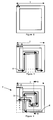
- the magnetic core 1, shown in Figure 1 has a spiral shape.
- the spiral has two ends 2 connected to each other by a closing segment 3. Thus, the magnetic core 1 is closed.
- the magnetic core 1 consists of a first set 4 of five parallel branches and a second set of four parallel branches, substantially perpendicular to the branches of the first set 4.
- the spiral constituted by all the branches of the two sets 4 and 5 is thus rectangular.
- the connection constituted by the closing segment 3 is added to the spiral to form the magnetic core 1.
- the magnetic core 1 makes it possible to maximize the occupation of the space in the center of the core 1 and the corresponding micro-inductance.
- An annular inductor according to the prior art, shown in Figure 2, adapts particularly well to a square-shaped chip.
- the length of the developed ring depends on the outer perimeter of the chip. This geometry does not exploit the central part of the chip.
- FIG. 3 represents an improvement in the annular inductance, the meandering inductance described in the aforementioned Park article.
- the meandering inductance makes it possible to use the central zone by stretching one of the four branches of the ring so as to constitute one or more meanders covering the central part.
- This solution makes it possible to increase the length I of the constant surface core.
- the occupation of the central zone by the meandering core (FIG. 3) makes it possible to obtain a gain on the length I of the core of the order of 33%, with respect to the annular core ( Figure 2).
- By increasing the number N of turns according to the length I of the core a compromise is obtained with a gain on the inductance L of about 20% and a gain on the saturation current I sat of about 10%.
- the meandering inductance is optimal only in special cases where the width of the ring and the width of the branches satisfy certain geometry conditions. Indeed, the central zone must be large enough to allow the insertion of an integer number of meanders.
- the core has an overall width T
- the branches have a width W
- the spacing between two adjacent branches must be greater than a minimum spacing S.
- the width T global of the core must fulfill the condition: T ⁇ 2 ⁇ W + nm * 2 ⁇ W + ( 2 ⁇ nm + 1 ) * S .
- T 2 ⁇ W + nm * 2 ⁇ W + ( 2 ⁇ nm + 1 ) * S .
- the branches and the closure segment 3 have a preferential direction of propagation of the magnetic flux in dynamics.
- the magnetic axes of the branches and the closing segment 3 are oriented relative to the other, so as to obtain a flow in the form of a closed loop as represented in FIG. 4 by the arrows 6.
- the branches can be arranged in different parallel planes.
- the first set of parallel branches is arranged in a first plane and the second set of parallel branches is arranged in a second plane, parallel to the first plane and greater than the first plane in FIG.
- the branches can have different thicknesses.
- the branches of the first set 4 are less thick than the branches of the second set 5. This makes it possible in particular to adapt the core to the local constraints of the chip used and the adjacent electronic components.
- One or more air gaps may optionally cut the magnetic core 1 to increase the reluctance of the magnetic circuit.
- the magnetic core 1 shown in FIG. 6 comprises several air gaps 11 of small size (at least a factor 1/10 between the dimension of the gap and the total length of the magnetic circuit).
- the gaps can be arranged in one or more branches.
- the branches constitute a spiral of rectangular type, or at least substantially rectangular, having two turns forming part of two concentric rectangles.
- the forms involved may be arbitrary, for example the geometry of the spiral is rectangular, round, square or octagonal.
- the person skilled in the art determines the particular form by using simulation software such as the Flux software from Cedrat or the Maxwell software from Ansoft.
- FIG. 7 illustrates a micro-inductance comprising the magnetic core 1 according to the invention.
- a plurality of disjointed turns 9 constitute a winding around the magnetic core 1.
- All the branches of the core may comprise winding turns.
- the turns envelop substantially all of the surface of the magnetic core 1, a minimum isolation gap separating the adjacent turns.
- Each turn may comprise a lower plane section in a lower plane, an upper plane section in an upper plane and two rising sections.
- the winding preferably comprises a single electrical input and a single electrical output.
- the closing segment 3 preferably has no turns 9.
- micro-inductance presents no additional manufacturing difficulties compared to conventional pre-existing systems.
- high permeability magnetic materials typically iron (Fe) and / or nickel (Ni) and / or cobalt (Co) alloys, which can contain one or more of aluminum, Al, Si, Tantalum, Hf, N, O, and B
- the core may be heterogeneous and consist of several ferromagnetic and conductive or dielectric (non-magnetic) or antiferromagnetic layers.
- the core may consist of an alternation of magnetic layers and intermediate layers, for example a stack comprising two magnetic layers separated by an intermediate layer.
- the intermediate layers may, for example, be metal (Cu copper, titanium Ti or ruthenium Ru, for example) or an insulating material such as silicon oxide SiO 2 or aluminum oxide Al 2 O 3 , for example.
- the intermediate layers may also consist of antiferromagnetic materials such as nickel oxide NiO or alloys of manganese (Mn) comprising nickel (NiMn), iridium (IrMn) or platinum (PtMn).
- the micro-inductance is not limited in its frequency of use, and may be suitable for high frequency uses, which always demand more power.
Landscapes
- Engineering & Computer Science (AREA)
- Power Engineering (AREA)
- Microelectronics & Electronic Packaging (AREA)
- Coils Or Transformers For Communication (AREA)
- Switches That Are Operated By Magnetic Or Electric Fields (AREA)
Abstract
Description
- L'invention est relative à un noyau magnétique fermé pour une micro-inductance intégrée.
- L'invention s'inscrit dans la thématique des micro-inductances intégrées pour des applications en électronique de puissance. Elle peut, d'une manière plus générale, s'appliquer à tous les systèmes inductifs (inductances, transformateurs, têtes d'enregistrement magnétique, actionneurs, capteurs, etc...) nécessitant une haute densité de puissance électrique.
- Il existe depuis de nombreuses années des micro-inductances de divers types, utilisant des bobinages de type spirale ou solénoïde. Cependant, les composants discrets restent très majoritairement utilisés dans des applications utilisant de fortes densités de puissance car ils offrent un meilleur compromis entre inductance et courant de saturation.
- Un bobinage de type spirale avec plan magnétique est facile à intégrer et permet de travailler à de forts courants. Cependant, ce type de dispositif devient très encombrant dès lors que l'on vise de fortes valeurs d'inductance (L de l'ordre du µH), parce qu'il faut un nombre de tours de spirale élevé. De plus, la résistance de tels dispositifs est importante.
- Les micro-inductances intégrées toroïdales avec bobinage solénoïde, ainsi que leurs améliorations en méandres (voir l'article « Integrated Electroplated Micromachined Magnetic Devices Using Low Temperature Fabrication Processes » by J.Y.Park et. al., IEEE Transactions on Electronics Packaging Manufacturing, Vol. 23, n°.1, 2000), sont directement inspirées des composants discrets et présentent le meilleur compromis possible entre résistance et niveau d'inductance, car on s'approche du cas idéal du solénoïde infini. Cependant, des simulations montrent que le flux magnétique à l'intérieur du noyau est réparti de façon très inhomogène. Le champ magnétique est plus intense le long des lignes de champ les plus courtes. Les zones du noyau magnétique soumises aux champs les plus intenses sont très rapidement saturées, provoquant une diminution de l'inductance dès des faibles courants, alors que d'autres zones sont soumises à des champs beaucoup plus faibles et ne participent que peu ou pas au phénomène inductif, c'est-à-dire elles n'ont pas de contribution à la valeur de l'inductance. Les zones utiles du noyau magnétique sont donc très vite saturées alors que d'autres zones restent non sollicitées.
- De plus, la puissance maximale passant dans une inductance est déterminée par le volume de matériau magnétique utilisé dans le cas d'un composant intégré. Ce volume est déterminé par l'épaisseur de matériau magnétique (épaisseurs inférieures à 100 microns pour des composants intégrés) et la surface occupée par ce noyau magnétique.
- Les transformateurs et inductances avec noyau magnétique en forme de E ou de E-1 sont très utilisés en électrotechnique, essentiellement dans des transformateurs discrets (et dans les dispositifs de type DC/DC discrets) afin de faciliter l'assemblage et le bobinage des inductances, ou bien pour pouvoir jouer sur les facteurs de conversion entre les trois bobinages de chaque branche, ou sur les effets d'inductances mutuelles entre les bobinages distincts de chaque branche (voir l'article « New Magnetic Structures for Switching Converters » de S.Cuk, IEEE Transactions on Magnetics, Vol. MAG-19, n°.2, 1983). Dans ces dispositifs, le bobinage n'est pas continu d'une branche à l'autre, mais réalisé par des fils distincts.
- La plupart des micro-inductances utilisées sur le marché sont des composants discrets fabriqués par des procédés micromécaniques de micro usinage, collage, micro-enroulement, etc... Ces procédés sont lourds à mettre en oeuvre, à traitement individuel, peu flexibles en termes de conception et limitent grandement la miniaturisation des circuits de puissance. En particulier, l'épaisseur des micro-inductances discrètes (typiquement supérieur à 0.5 mm) ne permet pas une mise en boîtier appropriée aux circuits d'alimentation utilisés actuellement pour la téléphonie mobile, par exemple.
- Les techniques de fabrications utilisées en microélectronique permettent une flexibilité bien plus grande au niveau de la mise en oeuvre de conceptions différentes, assurent un traitement collectif et sont compatibles avec l'idée de miniaturisation car l'épaisseur (substrat compris) peut facilement être inférieure à 300 µm). Cependant, elles sont mal adaptées au dépôt de fortes épaisseurs (supérieures à 10µm) de matériaux conducteurs, magnétiques ou diélectriques et à leur gravure après photolithographie.
- Pour les composants intégrés, on se heurte à des contraintes de réalisation technologique. En effet, des dépôts de couches conductrices ayant une épaisseur supérieure à 100 micromètres ne sont pour l'instant pas envisageable dans un procédé industriel standard.
- L'article « Numerical Inductor Optimization » de A. von der Weth et al. (Trans. Magn. Soc. Japan, Vol.2, No.5, pp.361-366, 2002) décrit une micro-inductance avec un circuit magnétique ouvert de type multi-branche. Une pluralité de spires disjointes les unes des autres constitue un bobinage autour des branches du noyau magnétique. Pour ces dispositifs, on cherche à augmenter le niveau d'inductance et à minimiser les pertes.
- Les micro-inductances intégrées présentent en général une inductance qui diminue fortement lorsque le courant appliqué aux spires de la micro-inductance est augmenté, même pour des courants faibles, ce qui oblige d'utiliser des inductances discrètes non-intégrées, dans certain cas.
- Les puces microélectroniques de petites dimensions (quelques millimètres au carré) sont généralement de forme carrée. L'intégration d'inductances impose donc des contraintes que l'on ne connaît pas pour les composants discrets. Les solutions proposées sont donc souvent complexes. Pour les inductances, en particulier, on cherche à minimiser la surface occupée, d'autant plus que le recours aux techniques de dépôt en couches minces limite grandement les épaisseurs utiles. En effet, la puissance d'une inductance Llsat 2 (L étant l'inductance et Isat le courant de saturation) dépend directement du volume de matériau magnétique disponible.
- L'objet de l'invention est d'augmenter la compacité d'un noyau d'une micro-inductance intégrée et, pour un encombrement donné, d'augmenter la valeur de l'inductance.
- Selon l'invention, ce but est atteint par un noyau magnétique selon les revendications annexées et plus particulièrement par le fait que le noyau magnétique a une forme de spirale comportant deux extrémités reliées l'une à l'autre par un segment de fermeture.
- L'invention a également pour but une micro-inductance intégrée comportant un noyau magnétique selon l'invention.
- D'autres avantages et caractéristiques ressortiront plus clairement de la description qui va suivre de modes particuliers de réalisation de l'invention donnés à titre d'exemples non limitatifs et représentés aux dessins annexés, dans lesquels :
- la figure 1 représente, en vue de perspective, un mode de réalisation particulier d'un noyau magnétique fermé selon l'invention,
- les figures 2 à 4 illustrent respectivement, en vue de dessus, deux noyaux magnétiques fermés selon l'art antérieur et un mode de réalisation particulier du noyau magnétique fermé selon l'invention,
- la figure 5 représente, en coupe selon l'axe A-A de la figure 4, un mode de réalisation particulier de l'invention,
- la figure 6 représente, en vue de dessus, un mode de réalisation particulier d'un noyau magnétique fermé selon l'invention,
- la figure 7 illustre un mode de réalisation particulier d'une micro-inductance intégrée selon l'invention.
- Le noyau magnétique 1, représenté sur la figure 1, a une forme de spirale. La spirale comporte deux extrémités 2 reliées l'une à l'autre par un segment de fermeture 3. Ainsi, le noyau magnétique 1 est fermé.
- Sur la figure 1, le noyau magnétique 1 est constitué par un premier jeu 4 de cinq branches parallèles et un second jeu 5 de quatre branches parallèles, sensiblement perpendiculaires aux branches du premier jeu 4. La spirale constituée par l'ensemble des branches des deux jeux 4 et 5 est ainsi rectangulaire. Le raccordement constitué par le segment de fermeture 3 s'ajoute à la spirale pour former le noyau magnétique 1.
- Comme illustré par l'intermédiaire des figures 2 à 4, le noyau magnétique 1 permet de maximiser l'occupation de l'espace au centre du noyau 1 et de la micro-inductance correspondante.
- On définit une longueur I du noyau magnétique, correspondant à la longueur développée du circuit magnétique, et le nombre N de spires du bobinage entourant le noyau magnétique 1. On peut démontrer, par l'intermédiaire du modèle des réluctances, les expressions suivantes (L étant l'inductance et Isat le courant de saturation) :


- Ainsi, pour augmenter la puissance de saturation Psat=LIsat 2 de l'inductance, on cherche à augmenter la longueur I du noyau magnétique. L'inductance L et le courant de saturation Isat résultent ainsi d'un compromis sur le nombre de spires N, qui est d'autant plus grand que la longueur I du noyau est grand.
- Une inductance annulaire selon l'art antérieur, représentée à la figure 2, s'adapte particulièrement bien à une puce de forme carrée. La longueur de l'anneau développé dépend du périmètre extérieur de la puce. Cette géométrie ne permet pas d'exploiter la partie centrale de la puce.
- La figure 3 représente une amélioration de l'inductance annulaire, l'inductance en méandres décrite dans l'article de Park précité. L'inductance en méandres permet d'utiliser la zone centrale en étirant l'une des quatre branches de l'anneau de manière à constituer un ou plusieurs méandres couvrant la partie centrale. Cette solution permet d'augmenter la longueur I du noyau à surface constante. En utilisant des règles de conception habituelles, l'occupation de la zone centrale par le noyau en méandres (figure 3) permet d'obtenir un gain sur la longueur I du noyau de l'ordre de 33%, par rapport au noyau annulaire (figure 2). En augmentant le nombre N de spires en fonction de la longueur I du noyau, on obtient un compromis avec un gain sur l'inductance L d'environ 20 % et un gain sur le courant de saturation Isat d'environ 10 %.
- Toutefois, l'inductance sous forme de méandres n'est optimale que dans des cas particuliers où la largeur de l'anneau et la largeur des branches vérifient certaines conditions de géométrie. En effet, la zone centrale doit être suffisamment grande pour permettre l'insertion d'un nombre entier de méandres.
- Comme représenté à la figure 3, le noyau a une largeur globale T, les branches ont une largeur W et l'espacement entre deux branches adjacentes doit être supérieur à un espacement minimum S. Ainsi, pour un nombre Nm de méandres donné, la largeur globale T du noyau doit remplir la condition :

- Le rapport du nombre Nm de méandres sur la surface de la zone centrale est maximisé lorsque la partie gauche et la partie droite de l'équation sont égales :

- En admettant que la largeur W des branches et l'espacement minimum S sont égaux (S=W) la condition se simplifie :

où T/W est le rapport de la largeur globale T sur la largeur W des branches. Pour T/W=7, 11, 15..., le noyau en méandres permet donc de remplir la zone centrale de façon optimale. Pour T/W=9, 13, 17... cependant, une partie importante de la zone centrale reste inutilisée. La mise en oeuvre de noyaux en méandres est donc restrictive dans la pratique puisque la taille de la puce et la largeur des branches sont en général imposées de façon indépendante. Une partie de la zone centrale peut ainsi rester inutilisée. - Le noyau magnétique 1 fermé en forme de spirale présente une plus grande indépendance vis-à-vis des contraintes dimensionnelles, et permet ainsi d'optimiser la longueur I du noyau, l'inductance L et le courant de saturation Isat pour une surface donnée quelconque. Comme précédemment, le gain sur la longueur de noyau I et le gain en puissance du noyau en spirale (figure 4) peuvent être évalués vis-à-vis de la structure annulaire de référence (figure 2). Il convient alors de distinguer deux cas :
- Lorsque le rapport T/W équivaut essentiellement à la partie de droite de l'équation ci-dessus, c'est-à-dire lorsque

le noyau en spirale fermé et le noyau en méandres sont comparables, car le gain sur la longueur et le gain sur la puissance sont comparables. - Lorsque l'équation ci-dessus n'est pas vérifiée, le noyau en spirale fermée permet d'obtenir un gain en longueur I et un gain en puissance plus importants que le noyau en méandres, par exemple pour T/W compris entre 8 et 10 (8<T/W<10) ou pour T/W compris entre 12 et 14 (12<T/W<14).
- En particulier, dans le cas d'un rapport T/W = 9, le noyau en spirale (figure 4) permet d'obtenir 53% de gain sur la longueur I et sur la puissance, par rapport à l'anneau (figure 2).
- Les branches et le segment de fermeture 3 ont une direction préférentielle de propagation du flux magnétique en dynamique. Les axes magnétiques des branches et du segment de fermeture 3 sont orientés les uns par rapport aux autres, de manière à obtenir un flux sous forme d'une boucle fermée comme représenté à la figure 4 par les flèches 6.
- Les branches peuvent être disposées dans des plans différents parallèles. Ainsi, comme représenté à la figure 5, le premier jeu 4 de branches parallèles est disposé dans un premier plan et le second jeu 5 de branches parallèles est disposé dans un second plan, parallèle au premier plan et supérieur au premier plan sur la figure 5. Par ailleurs, les branches peuvent avoir des épaisseurs différentes. Ainsi, sur la figure 5 les branches du premier jeu 4 sont moins épaisses que les branches du second jeu 5. Ceci permet notamment d'adapter le noyau aux contraintes locales de la puce utilisée et des composants électroniques adjacents.
- Un ou plusieurs entrefers peuvent éventuellement couper le noyau magnétique 1 afin d'augmenter la réluctance du circuit magnétique. Le noyau magnétique 1 représenté à la figure 6 comporte plusieurs entrefers 11 de dimension faible (au moins un facteur 1 /10 entre la dimension de l'entrefer et la longueur totale du circuit magnétique). Les entrefers peuvent être disposés dans une ou plusieurs des branches.
- Comme représenté aux figures 1, 4 et 6, les branches constituent une spirale de type rectangulaire, ou au moins sensiblement rectangulaire, ayant deux spires s'inscrivant dans deux rectangles concentriques. Cependant, selon les besoins, des spirales plus complexes peuvent être envisagées. Les formes mises en jeu peuvent être quelconques, par exemple la géométrie de la spirale est rectangulaire, ronde, carrée ou octogonale. L'homme du métier détermine la forme particulière en utilisant des logiciels de simulation tels que le logiciel Flux de la société Cedrat ou le logiciel Maxwell de la société Ansoft.
- La figure 7 illustre une micro-inductance comportant le noyau magnétique 1 selon l'invention. Une pluralité de spires 9 disjointes constitue un bobinage autour du noyau magnétique 1. Toutes les branches du noyau peuvent comporter des spires de bobinage. De préférence, les spires enveloppent la quasi-totalité de la surface du noyau magnétique 1, un écart d'isolement minimum séparant les spires adjacentes. Chaque spire peut comporter une section plane inférieure dans un plan inférieur, une section plane supérieure dans un plan supérieur et deux sections montantes. Le bobinage comporte, de préférence, une entrée électrique unique et une sortie électrique unique. Le segment de fermeture 3 ne comporte, de préférence, pas de spires 9.
- Pour les composants intégrés utilisant des techniques de micro-fabrication classiques, la micro-inductance ne présente aucune difficulté de fabrication additionnelle par rapport aux systèmes conventionnels préexistants.
- Pour le noyau magnétique 1, on utilise des matériaux magnétiques à forte perméabilité (supérieure à 10), typiquement des alliages à base de fer (Fe) et/ou de nickel (Ni) et/ou de cobalt (Co) et pouvant contenir l'un ou plusieurs des éléments suivants : aluminium (Al), silicium (Si), tantale (Ta), hafnium (Hf), azote (N), oxygène (O) et bore (B). Le noyau peut être hétérogène et constitué de plusieurs couches ferromagnétiques et conductrices ou diélectriques (non magnétiques) ou antiferromagnétiques. En particulier, le noyau peut être constitué d'une alternance de couches magnétiques et de couches intermédiaires, par exemple un empilement comportant deux couches magnétiques séparées par une couche intermédiaire. Les couches intermédiaires peuvent, par exemple, être en métal (cuivre Cu, titane Ti ou ruthénium Ru, par exemple) ou en un matériau isolant comme l'oxyde de silicium SiO2 ou l'oxyde d'aluminium Al2O3, par exemple. Les couches intermédiaires peuvent également être constituées par des matériaux antiferromagnétiques comme l'oxyde de nickel NiO ou les alliages de manganèse (Mn) comportant du nickel (NiMn), de l'iridium (IrMn) ou du platine (PtMn).
- La micro-inductance n'est pas limitée dans sa fréquence d'utilisation, et pourrait convenir à des utilisations à haute fréquence, qui réclament toujours plus de puissance. On peut alors très bien imaginer de tels composants travaillant dans la gamme des micro-ondes et remplaçant les inductances intégrées ou discrètes, avec ou sans matériau magnétique, qui sont habituellement utilisées. On retrouve alors des applications de type filtrage, adaptation d'impédance, etc.
Claims (9)
- Noyau magnétique (1) fermé pour une micro-inductance intégrée, caractérisé en ce qu'il a une forme de spirale comportant deux extrémités (2) reliées l'une à l'autre par un segment de fermeture (3).
- Noyau magnétique (1) selon la revendication 1, caractérisé en ce qu'il a une forme de spirale de type rectangulaire.
- Noyau magnétique (1) selon l'une des revendications 1 et 2, caractérisé en ce que le noyau magnétique (1) est constitué par une pluralité de branches.
- Noyau magnétique (1) selon la revendication 3, caractérisé en ce qu'au moins deux branches sont disposées dans des plans différents parallèles.
- Noyau magnétique (1) selon la revendication 4, caractérisé en ce qu'un premier jeu (4) de branches parallèles est disposé dans un premier plan et un second jeu (5) de branches parallèles est disposé dans un second plan.
- Noyau magnétique (1) selon la revendication 5, caractérisé en ce que les branches du premier jeu (4) de branches parallèles sont sensiblement perpendiculaires aux branches du second jeu (5) de branches parallèles.
- Noyau magnétique (1) selon l'une quelconque des revendications 3 à 6, caractérisé en ce qu'au moins deux branches ont des épaisseurs différentes.
- Noyau magnétique (1) selon l'une quelconque des revendications 1 à 7, caractérisé en ce qu'il comporte au moins un entrefer (11).
- Micro-inductance intégrée, caractérisée en ce qu'elle comporte un noyau magnétique (1) selon l'une quelconque des revendications 1 à 8.
Applications Claiming Priority (1)
| Application Number | Priority Date | Filing Date | Title |
|---|---|---|---|
| FR0609714A FR2908231B1 (fr) | 2006-11-07 | 2006-11-07 | Noyau magnetique ferme en forme de spirale et micro-inductance integree comportant un tel noyau magnetique ferme |
Publications (2)
| Publication Number | Publication Date |
|---|---|
| EP1921640A1 true EP1921640A1 (fr) | 2008-05-14 |
| EP1921640B1 EP1921640B1 (fr) | 2009-08-26 |
Family
ID=38004847
Family Applications (1)
| Application Number | Title | Priority Date | Filing Date |
|---|---|---|---|
| EP07354060A Not-in-force EP1921640B1 (fr) | 2006-11-07 | 2007-11-06 | Noyau magnétique fermé en forme de spirale et micro-inductance intégrée comportant un tel noyau magnétique fermé |
Country Status (6)
| Country | Link |
|---|---|
| US (1) | US20080106364A1 (fr) |
| EP (1) | EP1921640B1 (fr) |
| JP (1) | JP2008187166A (fr) |
| AT (1) | ATE441193T1 (fr) |
| DE (1) | DE602007002139D1 (fr) |
| FR (1) | FR2908231B1 (fr) |
Families Citing this family (3)
| Publication number | Priority date | Publication date | Assignee | Title |
|---|---|---|---|---|
| US20150061815A1 (en) | 2013-09-04 | 2015-03-05 | International Business Machines Corporation | Planar inductors with closed magnetic loops |
| US10290414B2 (en) * | 2015-08-31 | 2019-05-14 | Qualcomm Incorporated | Substrate comprising an embedded inductor and a thin film magnetic core |
| US10600566B2 (en) | 2016-10-13 | 2020-03-24 | International Business Machines Corporation | Method for forming a planar, closed loop magnetic structure |
Citations (2)
| Publication number | Priority date | Publication date | Assignee | Title |
|---|---|---|---|---|
| DE3016067A1 (de) * | 1980-04-25 | 1981-10-29 | Siemens AG, 1000 Berlin und 8000 München | Hybridschaltung und verfahren zu deren herstellung |
| US6114937A (en) * | 1996-08-23 | 2000-09-05 | International Business Machines Corporation | Integrated circuit spiral inductor |
Family Cites Families (18)
| Publication number | Priority date | Publication date | Assignee | Title |
|---|---|---|---|---|
| US3465238A (en) * | 1967-10-02 | 1969-09-02 | Jacob Marlow | Position and velocity detecting apparatus |
| US4309655A (en) * | 1978-06-23 | 1982-01-05 | Lgz Landis & Gyr Zug Ag | Measuring transformer |
| JPS61196505A (ja) * | 1985-02-26 | 1986-08-30 | Nec Corp | インダクタンス構造体 |
| JPH01106410A (ja) * | 1987-10-20 | 1989-04-24 | Victor Co Of Japan Ltd | インダクタンス素子 |
| JPH0513235A (ja) * | 1991-07-03 | 1993-01-22 | Sumitomo Electric Ind Ltd | インダクタンス素子 |
| JPH07220932A (ja) * | 1994-02-04 | 1995-08-18 | Mitsubishi Electric Corp | コイル素子およびそのモジュール |
| JP2694114B2 (ja) * | 1994-02-28 | 1997-12-24 | 株式会社アモルファス・電子デバイス研究所 | 薄膜磁気素子及びその製造方法 |
| US5815062A (en) * | 1995-06-30 | 1998-09-29 | Hitachi Metal, Ltd. | Magnetic core |
| US5847518A (en) * | 1996-07-08 | 1998-12-08 | Hitachi Ferrite Electronics, Ltd. | High voltage transformer with secondary coil windings on opposing bobbins |
| TR199902411A2 (xx) * | 1998-11-02 | 2000-06-21 | Lincoln Global, Inc. | Do�ru ak�m kaynak makinas� i�in ��k�� bobini ve kullanma y�ntemi |
| JP2000283998A (ja) * | 1999-03-31 | 2000-10-13 | Osaki Electric Co Ltd | 電気量−磁束変換用の磁気回路 |
| US6815220B2 (en) * | 1999-11-23 | 2004-11-09 | Intel Corporation | Magnetic layer processing |
| FR2811135B1 (fr) * | 2000-06-29 | 2002-11-22 | Memscap | Microcomposant du type micro-inductance ou microtransformateur |
| US6700472B2 (en) * | 2001-12-11 | 2004-03-02 | Intersil Americas Inc. | Magnetic thin film inductors |
| JP3971697B2 (ja) * | 2002-01-16 | 2007-09-05 | Tdk株式会社 | 高周波用磁性薄膜及び磁気素子 |
| US6825749B1 (en) * | 2004-01-26 | 2004-11-30 | National Applied Research Laboratories National Chip Implementation Center | Symmetric crossover structure of two lines for RF integrated circuits |
| JP4541800B2 (ja) * | 2004-08-20 | 2010-09-08 | ルネサスエレクトロニクス株式会社 | インダクタを備えた半導体装置 |
| KR100688858B1 (ko) * | 2004-12-30 | 2007-03-02 | 삼성전기주식회사 | 스파이럴 3차원 인덕터를 내장한 인쇄회로기판 및 그 제조방법 |
-
2006
- 2006-11-07 FR FR0609714A patent/FR2908231B1/fr not_active Expired - Fee Related
-
2007
- 2007-10-10 US US11/907,215 patent/US20080106364A1/en not_active Abandoned
- 2007-10-30 JP JP2007281911A patent/JP2008187166A/ja active Pending
- 2007-11-06 AT AT07354060T patent/ATE441193T1/de not_active IP Right Cessation
- 2007-11-06 EP EP07354060A patent/EP1921640B1/fr not_active Not-in-force
- 2007-11-06 DE DE602007002139T patent/DE602007002139D1/de active Active
Patent Citations (2)
| Publication number | Priority date | Publication date | Assignee | Title |
|---|---|---|---|---|
| DE3016067A1 (de) * | 1980-04-25 | 1981-10-29 | Siemens AG, 1000 Berlin und 8000 München | Hybridschaltung und verfahren zu deren herstellung |
| US6114937A (en) * | 1996-08-23 | 2000-09-05 | International Business Machines Corporation | Integrated circuit spiral inductor |
Non-Patent Citations (4)
| Title |
|---|
| A. VON DER WETH ET AL.: "Numerical Inductor Optimization", TRANS. MAGN. SOC., vol. 2, no. 5, 2002, pages 361 - 366 |
| J.Y.PARK: "Integrated Electroplated Micromachined Magnetic Devices Using Low Temperature Fabrication Processes", IEEE TRANSACTIONS ON ELECTRONICS PACKAGING MANUFACTURING, vol. 23, no. 1, 2000 |
| JAE YEONG PARK ET AL: "Integrated Electroplated Micromachined Magnetic Devices Using Low Temperature Fabrication Processes", IEEE TRANSACTIONS ON ELECTRONICS PACKAGING MANUFACTURING, IEEE, PISCATAWAY, NY, US, vol. 23, no. 1, January 2000 (2000-01-01), XP011020016, ISSN: 1521-334X * |
| S.CUK: "New Magnetic Structures for Switching Converters", IEEE TRANSACTIONS ON MAGNETICS, vol. 19, no. 2, 1983 |
Also Published As
| Publication number | Publication date |
|---|---|
| FR2908231A1 (fr) | 2008-05-09 |
| ATE441193T1 (de) | 2009-09-15 |
| US20080106364A1 (en) | 2008-05-08 |
| DE602007002139D1 (de) | 2009-10-08 |
| JP2008187166A (ja) | 2008-08-14 |
| FR2908231B1 (fr) | 2009-01-23 |
| EP1921640B1 (fr) | 2009-08-26 |
Similar Documents
| Publication | Publication Date | Title |
|---|---|---|
| EP1187149A1 (fr) | Microcomposant du type micro-inductance ou micro-transformateur | |
| FR2793943A1 (fr) | Micro-composants du type micro-inductance ou micro- transformateur, et procede de fabrication de tels micro- composants | |
| US20090322458A1 (en) | Magnetic component | |
| US20070230042A1 (en) | Thin film device | |
| WO2017090736A1 (fr) | Élément à effet de magnétorésistance type à inversion de magnétisation de courant de spin, et procédé de fabrication de celui-ci | |
| KR20140077346A (ko) | 파워 인덕터 및 그 제조 방법 | |
| EP1916675B1 (fr) | Bobinage comportant plusieurs branches de bobinage et micro-inductance comportant l'un des bobinages | |
| EP3579255B1 (fr) | Circuit integre comportant une inductance variable | |
| EP1157395B1 (fr) | Composant electronique discret de type inductif, et procede de realisation de tels composants | |
| EP1921640B1 (fr) | Noyau magnétique fermé en forme de spirale et micro-inductance intégrée comportant un tel noyau magnétique fermé | |
| EP1953775B1 (fr) | Inductance multiniveaux | |
| EP3033755B1 (fr) | Composant ferrite pour application de puissance et procede de fabrication du composant | |
| FR2811135A1 (fr) | Microcomposant du type micro-inductance ou microtransformateur | |
| EP1302955A1 (fr) | Inductance et son procédé de fabrication | |
| FR2907589A1 (fr) | Micro-inductance integree comportant un noyau magnetique ferme de type multi-branche | |
| EP3506326A2 (fr) | Dispositif de filtrage inductif a noyau magnetique torique | |
| WO2008071886A1 (fr) | Bobinage solenoide optimise | |
| FR2819921A1 (fr) | Dispositif de transmission de donnees pour la transmission separee galvaniquement de signaux et utilisation du dispositif | |
| EP3391461B1 (fr) | Module de communication sans fil, plaque adaptee pour etre utilisee pour la fabrication dudit module et procede de fabrication dudit module. | |
| EP1178504A1 (fr) | Microcomposant du type micro-inductance ou microtransformateur | |
| FR3037187B1 (fr) | Composant inductif magnetoelectrique accorde de maniere electrostatique | |
| JP2019179899A (ja) | 磁気抵抗効果デバイス | |
| FR3166744A1 (fr) | Coefficient de couplage d'un transformateur | |
| FR2823365A1 (fr) | Enroulement electrique, son procede de realisation et composant electromagnetique integrant au moins un tel enroulement | |
| FR2576447A1 (fr) | Dispositif de lignes de transmission de courants faibles attenuant les parasites |
Legal Events
| Date | Code | Title | Description |
|---|---|---|---|
| PUAI | Public reference made under article 153(3) epc to a published international application that has entered the european phase |
Free format text: ORIGINAL CODE: 0009012 |
|
| AK | Designated contracting states |
Kind code of ref document: A1 Designated state(s): AT BE BG CH CY CZ DE DK EE ES FI FR GB GR HU IE IS IT LI LT LU LV MC MT NL PL PT RO SE SI SK TR |
|
| AX | Request for extension of the european patent |
Extension state: AL BA HR MK RS |
|
| 17P | Request for examination filed |
Effective date: 20081105 |
|
| AKX | Designation fees paid |
Designated state(s): AT BE BG CH CY CZ DE DK EE ES FI FR GB GR HU IE IS IT LI LT LU LV MC MT NL PL PT RO SE SI SK TR |
|
| GRAP | Despatch of communication of intention to grant a patent |
Free format text: ORIGINAL CODE: EPIDOSNIGR1 |
|
| GRAS | Grant fee paid |
Free format text: ORIGINAL CODE: EPIDOSNIGR3 |
|
| GRAA | (expected) grant |
Free format text: ORIGINAL CODE: 0009210 |
|
| AK | Designated contracting states |
Kind code of ref document: B1 Designated state(s): AT BE BG CH CY CZ DE DK EE ES FI FR GB GR HU IE IS IT LI LT LU LV MC MT NL PL PT RO SE SI SK TR |
|
| REG | Reference to a national code |
Ref country code: GB Ref legal event code: FG4D Free format text: NOT ENGLISH |
|
| REG | Reference to a national code |
Ref country code: CH Ref legal event code: EP |
|
| REG | Reference to a national code |
Ref country code: IE Ref legal event code: FG4D Free format text: LANGUAGE OF EP DOCUMENT: FRENCH |
|
| REF | Corresponds to: |
Ref document number: 602007002139 Country of ref document: DE Date of ref document: 20091008 Kind code of ref document: P |
|
| LTIE | Lt: invalidation of european patent or patent extension |
Effective date: 20090826 |
|
| PG25 | Lapsed in a contracting state [announced via postgrant information from national office to epo] |
Ref country code: IS Free format text: LAPSE BECAUSE OF FAILURE TO SUBMIT A TRANSLATION OF THE DESCRIPTION OR TO PAY THE FEE WITHIN THE PRESCRIBED TIME-LIMIT Effective date: 20091226 Ref country code: AT Free format text: LAPSE BECAUSE OF FAILURE TO SUBMIT A TRANSLATION OF THE DESCRIPTION OR TO PAY THE FEE WITHIN THE PRESCRIBED TIME-LIMIT Effective date: 20090826 Ref country code: LT Free format text: LAPSE BECAUSE OF FAILURE TO SUBMIT A TRANSLATION OF THE DESCRIPTION OR TO PAY THE FEE WITHIN THE PRESCRIBED TIME-LIMIT Effective date: 20090826 Ref country code: SE Free format text: LAPSE BECAUSE OF FAILURE TO SUBMIT A TRANSLATION OF THE DESCRIPTION OR TO PAY THE FEE WITHIN THE PRESCRIBED TIME-LIMIT Effective date: 20090826 Ref country code: FI Free format text: LAPSE BECAUSE OF FAILURE TO SUBMIT A TRANSLATION OF THE DESCRIPTION OR TO PAY THE FEE WITHIN THE PRESCRIBED TIME-LIMIT Effective date: 20090826 |
|
| NLV1 | Nl: lapsed or annulled due to failure to fulfill the requirements of art. 29p and 29m of the patents act | ||
| PG25 | Lapsed in a contracting state [announced via postgrant information from national office to epo] |
Ref country code: LV Free format text: LAPSE BECAUSE OF FAILURE TO SUBMIT A TRANSLATION OF THE DESCRIPTION OR TO PAY THE FEE WITHIN THE PRESCRIBED TIME-LIMIT Effective date: 20090826 Ref country code: SI Free format text: LAPSE BECAUSE OF FAILURE TO SUBMIT A TRANSLATION OF THE DESCRIPTION OR TO PAY THE FEE WITHIN THE PRESCRIBED TIME-LIMIT Effective date: 20090826 Ref country code: NL Free format text: LAPSE BECAUSE OF FAILURE TO SUBMIT A TRANSLATION OF THE DESCRIPTION OR TO PAY THE FEE WITHIN THE PRESCRIBED TIME-LIMIT Effective date: 20090826 Ref country code: PL Free format text: LAPSE BECAUSE OF FAILURE TO SUBMIT A TRANSLATION OF THE DESCRIPTION OR TO PAY THE FEE WITHIN THE PRESCRIBED TIME-LIMIT Effective date: 20090826 |
|
| RAP2 | Party data changed (patent owner data changed or rights of a patent transferred) |
Owner name: COMMISSARIAT A L'ENERGIE ATOMIQUE |
|
| PG25 | Lapsed in a contracting state [announced via postgrant information from national office to epo] |
Ref country code: BG Free format text: LAPSE BECAUSE OF FAILURE TO SUBMIT A TRANSLATION OF THE DESCRIPTION OR TO PAY THE FEE WITHIN THE PRESCRIBED TIME-LIMIT Effective date: 20091126 Ref country code: PT Free format text: LAPSE BECAUSE OF FAILURE TO SUBMIT A TRANSLATION OF THE DESCRIPTION OR TO PAY THE FEE WITHIN THE PRESCRIBED TIME-LIMIT Effective date: 20091228 Ref country code: CY Free format text: LAPSE BECAUSE OF FAILURE TO SUBMIT A TRANSLATION OF THE DESCRIPTION OR TO PAY THE FEE WITHIN THE PRESCRIBED TIME-LIMIT Effective date: 20090826 |
|
| REG | Reference to a national code |
Ref country code: IE Ref legal event code: FD4D |
|
| PG25 | Lapsed in a contracting state [announced via postgrant information from national office to epo] |
Ref country code: DK Free format text: LAPSE BECAUSE OF FAILURE TO SUBMIT A TRANSLATION OF THE DESCRIPTION OR TO PAY THE FEE WITHIN THE PRESCRIBED TIME-LIMIT Effective date: 20090826 Ref country code: ES Free format text: LAPSE BECAUSE OF FAILURE TO SUBMIT A TRANSLATION OF THE DESCRIPTION OR TO PAY THE FEE WITHIN THE PRESCRIBED TIME-LIMIT Effective date: 20091207 Ref country code: IE Free format text: LAPSE BECAUSE OF FAILURE TO SUBMIT A TRANSLATION OF THE DESCRIPTION OR TO PAY THE FEE WITHIN THE PRESCRIBED TIME-LIMIT Effective date: 20090826 Ref country code: EE Free format text: LAPSE BECAUSE OF FAILURE TO SUBMIT A TRANSLATION OF THE DESCRIPTION OR TO PAY THE FEE WITHIN THE PRESCRIBED TIME-LIMIT Effective date: 20090826 Ref country code: RO Free format text: LAPSE BECAUSE OF FAILURE TO SUBMIT A TRANSLATION OF THE DESCRIPTION OR TO PAY THE FEE WITHIN THE PRESCRIBED TIME-LIMIT Effective date: 20090826 Ref country code: CZ Free format text: LAPSE BECAUSE OF FAILURE TO SUBMIT A TRANSLATION OF THE DESCRIPTION OR TO PAY THE FEE WITHIN THE PRESCRIBED TIME-LIMIT Effective date: 20090826 |
|
| BERE | Be: lapsed |
Owner name: CENTRE NATIONAL DE LA RECHERCHE SCIENTIFIQUE Effective date: 20091130 Owner name: STMICROELECTRONICS SA Effective date: 20091130 Owner name: COMMISSARIAT A L'ENERGIE ATOMIQUE Effective date: 20091130 |
|
| PG25 | Lapsed in a contracting state [announced via postgrant information from national office to epo] |
Ref country code: SK Free format text: LAPSE BECAUSE OF FAILURE TO SUBMIT A TRANSLATION OF THE DESCRIPTION OR TO PAY THE FEE WITHIN THE PRESCRIBED TIME-LIMIT Effective date: 20090826 |
|
| PG25 | Lapsed in a contracting state [announced via postgrant information from national office to epo] |
Ref country code: MC Free format text: LAPSE BECAUSE OF NON-PAYMENT OF DUE FEES Effective date: 20091130 |
|
| PLBE | No opposition filed within time limit |
Free format text: ORIGINAL CODE: 0009261 |
|
| STAA | Information on the status of an ep patent application or granted ep patent |
Free format text: STATUS: NO OPPOSITION FILED WITHIN TIME LIMIT |
|
| 26N | No opposition filed |
Effective date: 20100527 |
|
| PG25 | Lapsed in a contracting state [announced via postgrant information from national office to epo] |
Ref country code: BE Free format text: LAPSE BECAUSE OF NON-PAYMENT OF DUE FEES Effective date: 20091130 Ref country code: GR Free format text: LAPSE BECAUSE OF FAILURE TO SUBMIT A TRANSLATION OF THE DESCRIPTION OR TO PAY THE FEE WITHIN THE PRESCRIBED TIME-LIMIT Effective date: 20091127 |
|
| PGFP | Annual fee paid to national office [announced via postgrant information from national office to epo] |
Ref country code: DE Payment date: 20101119 Year of fee payment: 4 |
|
| PG25 | Lapsed in a contracting state [announced via postgrant information from national office to epo] |
Ref country code: LU Free format text: LAPSE BECAUSE OF NON-PAYMENT OF DUE FEES Effective date: 20091106 Ref country code: MT Free format text: LAPSE BECAUSE OF FAILURE TO SUBMIT A TRANSLATION OF THE DESCRIPTION OR TO PAY THE FEE WITHIN THE PRESCRIBED TIME-LIMIT Effective date: 20090826 |
|
| PG25 | Lapsed in a contracting state [announced via postgrant information from national office to epo] |
Ref country code: HU Free format text: LAPSE BECAUSE OF FAILURE TO SUBMIT A TRANSLATION OF THE DESCRIPTION OR TO PAY THE FEE WITHIN THE PRESCRIBED TIME-LIMIT Effective date: 20100227 |
|
| PG25 | Lapsed in a contracting state [announced via postgrant information from national office to epo] |
Ref country code: TR Free format text: LAPSE BECAUSE OF FAILURE TO SUBMIT A TRANSLATION OF THE DESCRIPTION OR TO PAY THE FEE WITHIN THE PRESCRIBED TIME-LIMIT Effective date: 20090826 |
|
| PG25 | Lapsed in a contracting state [announced via postgrant information from national office to epo] |
Ref country code: IT Free format text: LAPSE BECAUSE OF NON-PAYMENT OF DUE FEES Effective date: 20101106 |
|
| PGFP | Annual fee paid to national office [announced via postgrant information from national office to epo] |
Ref country code: IT Payment date: 20101130 Year of fee payment: 4 |
|
| PGFP | Annual fee paid to national office [announced via postgrant information from national office to epo] |
Ref country code: FR Payment date: 20111130 Year of fee payment: 5 |
|
| REG | Reference to a national code |
Ref country code: CH Ref legal event code: PL |
|
| PG25 | Lapsed in a contracting state [announced via postgrant information from national office to epo] |
Ref country code: CH Free format text: LAPSE BECAUSE OF NON-PAYMENT OF DUE FEES Effective date: 20111130 Ref country code: LI Free format text: LAPSE BECAUSE OF NON-PAYMENT OF DUE FEES Effective date: 20111130 |
|
| GBPC | Gb: european patent ceased through non-payment of renewal fee |
Effective date: 20121106 |
|
| REG | Reference to a national code |
Ref country code: FR Ref legal event code: ST Effective date: 20130731 |
|
| PG25 | Lapsed in a contracting state [announced via postgrant information from national office to epo] |
Ref country code: IT Free format text: LAPSE BECAUSE OF NON-PAYMENT OF DUE FEES Effective date: 20121106 |
|
| REG | Reference to a national code |
Ref country code: DE Ref legal event code: R119 Ref document number: 602007002139 Country of ref document: DE Effective date: 20130601 |
|
| PG25 | Lapsed in a contracting state [announced via postgrant information from national office to epo] |
Ref country code: DE Free format text: LAPSE BECAUSE OF NON-PAYMENT OF DUE FEES Effective date: 20130601 |
|
| PG25 | Lapsed in a contracting state [announced via postgrant information from national office to epo] |
Ref country code: FR Free format text: LAPSE BECAUSE OF NON-PAYMENT OF DUE FEES Effective date: 20121130 Ref country code: GB Free format text: LAPSE BECAUSE OF NON-PAYMENT OF DUE FEES Effective date: 20121106 |