EP1919068A2 - Regulator for isolated flyback power supply using primary side sensing - Google Patents
Regulator for isolated flyback power supply using primary side sensing Download PDFInfo
- Publication number
- EP1919068A2 EP1919068A2 EP07113960A EP07113960A EP1919068A2 EP 1919068 A2 EP1919068 A2 EP 1919068A2 EP 07113960 A EP07113960 A EP 07113960A EP 07113960 A EP07113960 A EP 07113960A EP 1919068 A2 EP1919068 A2 EP 1919068A2
- Authority
- EP
- European Patent Office
- Prior art keywords
- value
- circuit
- regulator
- sample
- cause
- Prior art date
- Legal status (The legal status is an assumption and is not a legal conclusion. Google has not performed a legal analysis and makes no representation as to the accuracy of the status listed.)
- Withdrawn
Links
Images


Classifications
-
- H—ELECTRICITY
- H02—GENERATION; CONVERSION OR DISTRIBUTION OF ELECTRIC POWER
- H02M—APPARATUS FOR CONVERSION BETWEEN AC AND AC, BETWEEN AC AND DC, OR BETWEEN DC AND DC, AND FOR USE WITH MAINS OR SIMILAR POWER SUPPLY SYSTEMS; CONVERSION OF DC OR AC INPUT POWER INTO SURGE OUTPUT POWER; CONTROL OR REGULATION THEREOF
- H02M3/00—Conversion of DC power input into DC power output
- H02M3/22—Conversion of DC power input into DC power output with intermediate conversion into AC
- H02M3/24—Conversion of DC power input into DC power output with intermediate conversion into AC by static converters
- H02M3/28—Conversion of DC power input into DC power output with intermediate conversion into AC by static converters using discharge tubes with control electrode or semiconductor devices with control electrode to produce the intermediate AC
- H02M3/325—Conversion of DC power input into DC power output with intermediate conversion into AC by static converters using discharge tubes with control electrode or semiconductor devices with control electrode to produce the intermediate AC using devices of a triode or a transistor type requiring continuous application of a control signal
- H02M3/335—Conversion of DC power input into DC power output with intermediate conversion into AC by static converters using discharge tubes with control electrode or semiconductor devices with control electrode to produce the intermediate AC using devices of a triode or a transistor type requiring continuous application of a control signal using semiconductor devices only
- H02M3/33507—Conversion of DC power input into DC power output with intermediate conversion into AC by static converters using discharge tubes with control electrode or semiconductor devices with control electrode to produce the intermediate AC using devices of a triode or a transistor type requiring continuous application of a control signal using semiconductor devices only with automatic control of the output voltage or current, e.g. flyback converters
Definitions
- This disclosure pertains to regulators for power supplies and, more particularly, to regulators for isolated flyback power supplies that use primary side sensing.
- Power supplies that are used in telecommunications, health care, industry, and other applications may require electrical isolation between the input to the supply and the output from the supply.
- a transformer is often used to provide this isolation.
- the transformer is often configured in what is known as a flyback converter.
- a flyback converter often regulates the output of the power supply by controlling a series of pulses that are delivered to the primary winding of the transformer. When the output needs to be increased, the on-time and/or the frequency of the pulses may be increased. Conversely, when the output needs to be decreased, the reverse may take place.
- the output of the supply is usually sensed. When complete electrical isolation must be maintained between the input and the output, this sensing must also be done in an electrically isolated manner.
- an optoisolator is sometimes used to relay the output level back to the input control system.
- the feedback in this configuration utilizes an optical path over which electrons cannot travel.
- Optoisolators can increase the size of the power supply, increase costs, and may limit the ability of the power supply to make needed adjustments quickly.
- the output regulation that is accomplished using primary side sensing may not be adequate.
- the regulation may not be as fast and/or as accurate as is needed. Efforts to improve the regulation, moreover, may cause the effectiveness of the regulator to become dependent upon the specific characteristics of the transformer that is used with it. This may make it difficult to design a single regulator that can be effectively used with a broad variety of transformers.
- a power supply having a transformer with a primary winding configured to be repeatedly coupled to and decoupled from an energy-supplying circuit and a secondary winding coupled to a diode may be regulated.
- the regulator may include an error circuit configured to generate an error signal representative of the difference between a target value and a measured value, a sample and hold circuit, and a controller circuit.
- the controller circuit may be configured to cause the sample and hold circuit to sample the value of a derived signal that is derived from a connection to the primary winding at a time when the primary winding is decoupled from the energy-supplying circuit and the diode is conducting current.
- the controller circuit may also be configured to cause the sample and hold circuit to hold the sampled value at least until the diode stops conducting current.
- the controller circuit may also be configured to cause the held value to be the measured value used by the error circuit.
- FIG. 1 illustrates a portion of an isolated flyback power supply using primary side sensing and a regulator.
- FIG. 2 is an example of the output voltage derivation circuit that is shown in FIG. 1.
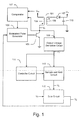
- FIG. 3 is an example of the sample and hold circuit that is shown in FIG. 1.
- FIG. 4 is an example of the controller circuit that is shown in FIG. 1.
- FIG. 5 illustrates signals that may be found in one or more of the circuits illustrated in FIGS. 1-4.
- FIG. 1 illustrates a portion of an isolated flyback power supply using primary side sensing and a regulator.
- the output of the power supply may be represented as V O .
- the power supply may include a transformer 101 having a primary winding 103 and a secondary winding 106.
- the secondary winding 106 may be connected to a rectifying diode 107 and a filtering capacitor 110.
- the rectifying diode 107 may be of any type. For example, it may be a Schottky diode.
- the filtering capacitor 110 may be of any type. Numerous other types of rectifying and/or filtering circuits may be used in addition and/or instead. -For example, multiple secondary windings may be used with rectifying diodes to generate multiple output voltages.
- the primary winding 103 may be connected to an energy-supplying circuit.
- one of the leads to the primary winding 103 may be connected to a source of energy, such as V IN , while the other lead may be connected to a switching circuit, such as a transistor 105.
- Other types of switching circuits may be used in addition or instead, such as switching circuits that use MOSFETs and/or any other type of controllable switch or switches.
- a modulated pulse generator 108 may be used to drive the switching circuit.
- the modulated pulse generator 108 may be configured to deliver a series of pulses to the switching circuit, thus causing the primary winding 103 of the transformer 101 to be repeatedly coupled to and decoupled from the energy-supplying circuit.
- the modulated pulse generator 108 may be configured to vary the pattern of the pulses that are delivered to the switching circuit, thus varying the amount of energy that is delivered into the transformer 101. In turn, this may affect the output voltage V O of the power supply.
- the primary voltage V P on the primary winding 103 may contain information indicative of the output voltage V O from the power supply. This may occur during periods when the pulses from the modulated pulse generator 108 are off, that is, when the transistor 105 is off, and current is traveling through the secondary winding 106 and hence the diode 107. During these periods, the primary voltage V P across the primary winding 103 may be approximately equal to V IN plus V O , times the ratio of the turns in the primary and secondary windings.
- An output voltage derivation circuit 109 may be configured to derive a derived voltage V D that is representative of the output voltage V O from V P . More specifically, it may be configured to level shift V P by subtracting V IN from V P . In addition to level shifting, the output voltage derivation circuit 109 may be configured to scale the level shifted value, an example of which is discussed below in connection with FIG. 2.
- the derived voltage V D from the output voltage derivation circuit 109 may be coupled to a sample and hold circuit 113.
- the sample and hold circuit 113 may be configured to sample V D and to hold this value.
- the derived voltage V D from the output voltage derivation circuit 109 may also be coupled to a controller circuit 111.
- the controller circuit 111 may be configured to cause the sample and hold circuit 113 to sample V D at one or more times and to hold one or more sampled values until one or more other times.
- the controller circuit 111 may be configured to cause the sample and hold circuit 113 to sample the value of V D when the primary winding 103 is decoupled from the energy-supplying circuit and when the diode 107 is conducting current.
- the controller circuit 111 may also be configured to cause the sample and hold circuit 113 to hold that sampled value - i.e., to preserve the sampled value even while the input V D later changes -- at least until the diode 107 stops conducting current.
- the controller circuit 111 may also be configured to cause the sample and hold circuit 113 to deliver a sampled value that is held to an error circuit 115 as a measured voltage V M .
- the error circuit 115 may be configured to generate an error voltage V E that is representative of the difference between a target voltage V T and a measured voltage V M .
- the error voltage V E may be coupled to the modulated pulse generator 108.
- the modulated pulse generator 108 may be configured to alter the pattern of pulses to the transistor 105, so as to cause V M to approach and ultimately equal V T , thus effectively causing the output voltage V O of the power supply to be at a desired level, as controlled by the value of V T .
- any one or more of a broad variety of circuits may be used by the modulated pulse generator 108 to adjust the pattern of pulses to the transistor 105 in response to the error voltage V E .
- the modulated pulse generator 108 may utilize pulse width modulation.
- the modulated pulse generator 108 may be configured to vary the width of the pulses to the transistor 105 in relation to the error voltage V E . If the error voltage V E indicates that output voltage V O is too low, for example, the modulated pulse generator 108 may be configured to increase the width of each pulse. Conversely, if the error voltage V E indicates that the output voltage V O is too high, the modulated pulse generator 108 may be configured to decrease the width of each pulse.
- V E voltage-mode PWM
- V E current limit
- the period of each pulse may remain constant. Under certain conditions, this may cause the transistor 105 to remain open while no current is being conducted through the diode 107.
- This may require the transformer 101 to be sized so that it is capable of delivering a needed quantity of energy during only a portion of its use. In turn, this may require a bulkier and potentially more expensive transformer than might otherwise be needed if the energy required by the load was supplied by the transformer over a greater portion of its switching cycle.
- the modulated pulse generator 108 may instead or in addition be configured to turn the transistor 105 back on as soon as the current through the diode 107 stops.
- a comparator 117 may be configured to compare V P with V IN and to signal the modulated pulse generator 108 that current through the diode 107 has ceased when Vp crosses a threshold that is just slightly higher than V IN .
- the modulated pulse generator 108 may be configured to then turn the pulse back on.
- V D may be compared to V T as an alternate or additional means of determining when the current through the diode 107 has stopped. When V D reaches approximately 90% of V T , for example, this may be interpreted by a comparator circuit (not shown) as meaning that the current through the diode 107 has stopped. Other techniques for determining when the current though the diode 107 stops may be used in addition or instead.
- Errors in the feedback system that has just been described can still be caused by a variety of factors. For example, errors can be caused by the voltage drop that may take place in the secondary winding 106 of the transformer due to its internal resistance. Errors may similarly be caused by the voltage drop caused by the diode 107. These voltage drops may cause the output voltage V O not to be truly reflected in the value of V P .
- the controller circuit 111 may be configured to cause the value of V D that is sampled and held to be the value that V D had just slightly before the diode 107 stops conducting current. At this point in time, the current through the diode 107 may be very low, thus minimizing the error that might otherwise be caused by the voltage drops caused by the internal resistance of the secondary winding 106 and the diode 107.
- the controller circuit 111 may also be configured to cause the sample and hold circuit 113 to deliver this just-before-the-current-stops held value of V D to the error circuit 115 as V M .
- the controller circuit 111 may be configured to cause this value to be held by the error circuit 115 as V M until the next cycle when the current through the diode 107 has again reached this low value and the held value may be updated with a more recent measurement.
- the moment when the controller circuit 111 causes the value of V D to be held may vary.
- the controller circuit 111 may be configured to cause the value of V D to be sampled and held by the sample and hold circuit 113 within no more than 300 nanoseconds before the current through the diode 107 stops.
- the cessation of curreny through the diode 107 stops may detected using the comparator 117 and/or or the other techniques discussed above and/or any other technique.
- the controller circuit 111 may be configured to cause the value of V D to in addition or instead be sampled and held when the amount of current through the diode 107 goes below 25% of its average conducting value, i.e., below 25% of the average value of the current that has been flowing through the diode 107 during one off period of the pulses to the transistor 105.
- FIG. 2 is an example of the output voltage derivation circuit 109 that is shown in FIG. 1.
- the circuit may include a transistor 201 configured as a diode, a transistor 203, a current supply 205, a resistor 207, and a resistor 209.
- the circuit may function as an emitter follower to force the emitter of the transistor 203 to V IN .
- the current supply 205 may be set at any amount needed to forward bias the diode-connected transistor 201. In one embodiment, a current of approximately 20 micro amps may be used.
- the values of the resistors 207 and 209 may be selected so as to control the scaling of the level-shifted voltage.
- the error circuit 115 may minimize the error between V D and V T with the aid of the sample and hold circuit 113.
- the voltage across the primary winding, V L -V IN may equal the voltage across the secondary times the turns ratio N of the transformer.
- V D may be approximately V T when the output voltage V O has reached the target output voltage V OT .
- the voltage V T may be 1.25 volts which may be called the bandgap voltage. When used in conjunction with appropriate circuitry, this value may minimize drifts and other temperature-dependent errors.
- FIG. 3 is an example of the sample and hold circuit 113 that is shown in FIG. 1.
- the circuit may include a buffer 301, a plurality of controllable switches, such as MOSFETs 303, 305, 307, and 309, and a plurality of storage devices, such as capacitors 311, 313, and 315.
- controllable switches and/or storage devices may be used in addition or instead, including FETS, BJTs, SCRs for the switches and/or inductors for the storage devices.
- MOSFET 303 may be configured to cause the capacitor 311 to charge to the value V D when a sample voltage V SB goes high.
- MOSFET 307 may similarly be configured to cause the capacitor 313 to charge to the value of V D when a sample voltage V SA goes high.
- MOSFET 305 may be configured to transfer charge from the capacitor 311 to the capacitor 315 when a transfer voltage V TB goes high.
- MOSFET 309 may be similarly be configured to transfer charge from the capacitor 313 to the capacitor 315 when a transfer voltage V TA goes high.
- MOSFETs 305 and 309 may collectively be considered to be a controllable switching network that may be controlled by appropriate transfer voltages V TB and V TA to cause the charge that is delivered to the capacitor 315 to come from either the capacitor 311 or the capacitor 313.
- the value of the capacitors 311 and 313 may be selected so as to be at least five times the value of the capacitor 315.
- the capacitors 311 and 313 may be approximately 10 picofarads, while the capacitor 315 may be 1 picofarad. This may cause the voltage that is on the capacitor 311 to be approximately copied to the capacitor 315 when the MOSFET 305 is closed. Similarly, this may cause the voltage that is on the capacitor 313 to be approximately copied to the capacitor 315 when the MOSFET 309 is closed.
- FIG. 4 is an example of the controller circuit 111 that is shown in FIG. 1.
- the controller circuit may include a clock 401, inverters 403 and 405, a divide-by-two circuit 407, and NOR gates 409, 411, 413, and 415.
- the clock 401 may be configured so as to be gated on and off by a feedback voltage V F .
- the feedback voltage V F may be a logic signal that goes high when the transistor 105 opens and goes low when the current through the diode 107 stops.
- the rising edges for V F may be derived from the rising edges of the pulses that are generated by the modulated pulse generator 108.
- the rising edges of V F may be delayed in certain embodiments so as to eliminate the processing of V D during its very early stages when it is reflecting spurious peak voltages due to leakage inductance in the transformer 101.
- the falling edges of V F may be derived from the falling edges of the derived voltage V D .
- Other means of generating V F may be used in addition or instead.
- the clock 401 may produce a clock voltage V C of any type and at any frequency.
- V C may oscillate at a frequency of between 4 MHz and 6 MHz, such as at a frequency of 5 MHz. It may have a duty cycle that is on for no more than 40% of the time, such as having a high period of approximately 70 nanoseconds and a low period of approximately 140 nanoseconds.
- the controller circuit may be configured as is shown in FIG. 4 to generate the voltages V SB , V SA , V TB , and V TA that are used by the circuit shown in FIG. 3.
- Other devices and/or configurations shown in FIG. 4 may be used in addition or instead. The nature of one example of these control voltages will now be discussed in connection with FIG. 5.
- FIG. 5 illustrates signals that may be found in one or more of the circuits illustrated in FIGS. 1-4.
- V D the voltage that is derived by the output voltage derivation circuit 109 shown in FIGS. 1 and FIG. 2.
- V D may represent a level shifted and scaled version of the output voltage V O while the transistor 105 is open and the diode 107 is conducting current.
- FIG. 5 also illustrates V F , the feedback voltage that may rise when the transistor 105 is open and may fall when the current though the diode 109 stops.
- FIG. 5 also illustrates the clock voltage V C . Because the clock 401 may be gated by V F , the clock signal V C may not begin until V F goes high.
- FIG. 5 also illustrates the sample voltages V SA and V SB that are generated by the controller circuit that is illustrated in FIG. As shown in FIG. 5, V SA may be shifted in phase from V SB .
- the controller circuit may also be configured to prevent V SA from overlapping with V SB , as also shown in FIG. 5.
- FIG. 5 also illustrates the held measured voltage V M from the sample and hold circuit 113, an example of which is illustrated in FIG. 3.
- V D may go high at a rising edge 501 as soon as the transistor 105 is opened. In turn, this may cause V F to go high at a rising edge 503, thus starting the generation of the clock pulses V C at a rising edge 505.
- the gating signal V SA may go high at a rising edge 507, causing the value of V D to be stored on the capacitor 313 in FIG. 3.
- the logic circuit in FIG. 4 may cause the first falling edge 509 of V C to turn off V SA at a falling edge 511, thus causing the last sampled value of V D to be held by the capacitor 313.
- the gating signal V SB may go high at a rising edge 517, causing the value of V D to be stored on the capacitor 311.
- the logic circuit shown in FIG. 4 may then cause the gating signal V SB to go low on the next falling edge 519 of V C at a falling edge 521, thus causing the last sampled value of V D to be held on the capacitor 311 .
- This process of causing the value of V D to be alternately sampled and held on the capacitors 311 and 313 may continue until such time as the current stops flowing through the diode 107, as reflected by a falling edge 523 of V D .
- V D may cause V F to go low at a falling edge 525 which may cause all further clock pulses to stop. What happens next may depend upon the state of the clock and the logic at the time that the current through the diode 107 stops.
- V C If the clock voltage V C is high when V F goes low, the falling edge of V F may cause V C to fall at a falling edge 527.
- V SA also happens to high when V F goes low
- the falling edge 525 of V F may also cause V SA to go low at a falling edge 529.
- This may cause the capacitor 313 to hold a zero or near zero value of V D that is not representative of V O .
- the last value of V D that was held before the current through the diode 107 stops may be the best representation of V O . In this example, this value was held in the capacitor 311.
- the logic shown in FIG. 4 thus causes V TB to go high, causing the value that was held in the capacitor 311 to be transferred to the capacitor 315. This may thus cause V M to change, as illustrated by a rising edge 531.
- V M is approximately equal to the voltage that was stored and last held in the capacitor 311, as reflected by a voltage point 533.
- V m could instead have gone down in value, up in a different amount, or remained substantially the same, all depending on any changes that might have occurred to output voltage V O since the previous cycle.
- the current through the diode 107 might instead stop flowing when V SB is high.
- the logic circuit shown in FIG. 4 may instead cause the transfer voltage V TA to go high when V F goes low, i.e., on the falling edge 525 of V F .
- This may instead cause the voltage on the capacitor 313 to transfer to the capacitor 315 , thus establishing the voltage on the capacitor 313 as the new value for V M .
- the current through the diode 107 may instead stop while V C is low.
- the logic circuit shown in FIG. 4 may cause the value that was last held to be transferred to the capacitor 315, be it have been in the capacitor 311 or the capacitor 313. If V SA was just high, for example, the transfer voltage V TB may go high. This may cause the voltage on capacitor 313 to transfer to the capacitor 315. This may be accomplished by causing either V TB or V TA to go high when V F goes low on its falling edge 525.
- the logic circuit shown in FIG. 4 may be configured to cause the last value that was held on either the storage capacitor 311 or 313 before the current through the diode 107 stops to be transferred to the capacitor 315 after the current through the diode 107 stops.
- This transferred value may serve as the measured voltage V M that is processed by the error circuit 115. This may insure that a valid value is used throughout the feedback process.
- This sequence of events may also help insure that the derived value of the output voltage V O that is used in the feedback circuit is based on a value of the primary voltage V P that existed just before the current through the diode 107 stopped, i.e., when the current was very low. As explained above, this may help minimize errors caused by the resistance in the secondary winding 106 of the transformer 101 and the non-linear voltage drop caused by the diode 107.
- the frequency of the clock signal V C may be selected to insure that the last held value of V D is always very close to the point when the diode 107 stops conducting current.
- the clock frequency may be selected such that the sample that is held by the capacitor 315 is taken within no more than 300 nanoseconds before the diode stops conducting current. If a clock frequency of approximately 5 MHz is selected, for example, the sample that is held and used as V M will have been taken within no more than 150 nanoseconds before the diode stops conducting current.
- the frequency of the clock pulses may be selected so that the last sample that is held is not taken until after the current flowing through the diode has dropped below 25% of its average conducting value.
- Other standards may be employed in addition or instead.
- Varying the duty cycle of the clock signal V C may assist in insuring that the held sample that is used as V M is taken before the V D voltage falls and becomes invalid. There may be some delay between when the V D becomes invalid and V F goes low.
- the clock 401 may be configured so as to cause the clock signal V C to be high for 40% or less of its period, such as to be high for approximately 70 nanoseconds and low for approximately 140 nanoseconds. Because of the logic circuit shown in FIG. 4, this unequal duty cycle may cause the width of each pulse in the sample voltages V SA and V SB to decrease, thus increasing the chance that a sample that is taken by a capacitor 311 or 313 will be held in that capacitor by the sample voltage V SA or V SB going low before the current through the diode 107 stops.
- the sampled value of V D that is held just prior to the falling edge 525 of V F could fail to contain an accurate representation of V O . This could be due to a lack of synchronism between V F and the actual shutdown of current through the diode 107 and/or a delay in recognizing its falling edge 525. The current through the diode 107 may also be too low at the time for an accurate reading. This could be particularly true when the falling edge 525 of V F takes place immediately following a falling edge of the clock voltage V C .
- the controller circuit 111 may be configured to cause the sample and hold circuit 113 to deliver the second-to last held value of V D as V M , rather than the last held value.
- the controller circuit 111 may instead be configured to deliver an even earlier-held value of V D , in which event the sample and hold circuit 113 may be modified to hold such an earlier value.
Landscapes
- Engineering & Computer Science (AREA)
- Power Engineering (AREA)
- Dc-Dc Converters (AREA)
Abstract
Description
- Technical Field
- This disclosure pertains to regulators for power supplies and, more particularly, to regulators for isolated flyback power supplies that use primary side sensing.
- Description of Related Art
- Power supplies that are used in telecommunications, health care, industry, and other applications may require electrical isolation between the input to the supply and the output from the supply. A transformer is often used to provide this isolation.
- The transformer is often configured in what is known as a flyback converter. A flyback converter often regulates the output of the power supply by controlling a series of pulses that are delivered to the primary winding of the transformer. When the output needs to be increased, the on-time and/or the frequency of the pulses may be increased. Conversely, when the output needs to be decreased, the reverse may take place.
- To determine how the pulses must be altered to achieve a desired output, the output of the supply is usually sensed. When complete electrical isolation must be maintained between the input and the output, this sensing must also be done in an electrically isolated manner.
- To achieve this electrical isolation, an optoisolator is sometimes used to relay the output level back to the input control system. The feedback in this configuration utilizes an optical path over which electrons cannot travel. Optoisolators, however, can increase the size of the power supply, increase costs, and may limit the ability of the power supply to make needed adjustments quickly.
- Another technique has been to monitor the voltage on the primary winding of the transformer in the flyback converter, commonly referred to as "primary side sensing." This monitoring has typically been done during each off period of the pulses when the primary winding has been disconnected from the supply voltage and while current is still traveling through the secondary winding of the transformer. This techniques works due to inherent characteristics of transformer. These inherent characteristics cause the voltage on the primary winding during this period to be approximately equal to the output voltage of the power supply, times the ratio of turns in the primary and secondary windings.
- The output regulation that is accomplished using primary side sensing, however, may not be adequate. The regulation may not be as fast and/or as accurate as is needed. Efforts to improve the regulation, moreover, may cause the effectiveness of the regulator to become dependent upon the specific characteristics of the transformer that is used with it. This may make it difficult to design a single regulator that can be effectively used with a broad variety of transformers.
- A power supply having a transformer with a primary winding configured to be repeatedly coupled to and decoupled from an energy-supplying circuit and a secondary winding coupled to a diode may be regulated. The regulator may include an error circuit configured to generate an error signal representative of the difference between a target value and a measured value, a sample and hold circuit, and a controller circuit. The controller circuit may be configured to cause the sample and hold circuit to sample the value of a derived signal that is derived from a connection to the primary winding at a time when the primary winding is decoupled from the energy-supplying circuit and the diode is conducting current. The controller circuit may also be configured to cause the sample and hold circuit to hold the sampled value at least until the diode stops conducting current. The controller circuit may also be configured to cause the held value to be the measured value used by the error circuit.
- Related power supplies and processes are also disclosed.
- These, as well as other components, steps, features, objects, benefits, and advantages, will now become clear from a review of the following detailed description of illustrative embodiments, the accompanying drawings, and the claims.
- FIG. 1 illustrates a portion of an isolated flyback power supply using primary side sensing and a regulator.
- FIG. 2 is an example of the output voltage derivation circuit that is shown in FIG. 1.
- FIG. 3 is an example of the sample and hold circuit that is shown in FIG. 1.
- FIG. 4 is an example of the controller circuit that is shown in FIG. 1.
- FIG. 5 illustrates signals that may be found in one or more of the circuits illustrated in FIGS. 1-4.
- FIG. 1 illustrates a portion of an isolated flyback power supply using primary side sensing and a regulator. The output of the power supply may be represented as VO.
- As shown in FIG. 1, the power supply may include a
transformer 101 having aprimary winding 103 and asecondary winding 106. Thesecondary winding 106 may be connected to a rectifyingdiode 107 and a filteringcapacitor 110. - The rectifying
diode 107 may be of any type. For example, it may be a Schottky diode. Similarly, the filteringcapacitor 110 may be of any type. Numerous other types of rectifying and/or filtering circuits may be used in addition and/or instead. -For example, multiple secondary windings may be used with rectifying diodes to generate multiple output voltages. - The
primary winding 103 may be connected to an energy-supplying circuit. For example, one of the leads to theprimary winding 103 may be connected to a source of energy, such as VIN, while the other lead may be connected to a switching circuit, such as atransistor 105. Other types of switching circuits may be used in addition or instead, such as switching circuits that use MOSFETs and/or any other type of controllable switch or switches. - A modulated
pulse generator 108 may be used to drive the switching circuit. The modulatedpulse generator 108 may be configured to deliver a series of pulses to the switching circuit, thus causing theprimary winding 103 of thetransformer 101 to be repeatedly coupled to and decoupled from the energy-supplying circuit. - The modulated
pulse generator 108 may be configured to vary the pattern of the pulses that are delivered to the switching circuit, thus varying the amount of energy that is delivered into thetransformer 101. In turn, this may affect the output voltage VO of the power supply. - Due to inherent characteristics of the
transformer 101 and as explained above, the primary voltage VP on theprimary winding 103 may contain information indicative of the output voltage VO from the power supply. This may occur during periods when the pulses from the modulatedpulse generator 108 are off, that is, when thetransistor 105 is off, and current is traveling through thesecondary winding 106 and hence thediode 107. During these periods, the primary voltage VP across theprimary winding 103 may be approximately equal to VIN plus VO, times the ratio of the turns in the primary and secondary windings. - An output
voltage derivation circuit 109 may be configured to derive a derived voltage VD that is representative of the output voltage VO from VP. More specifically, it may be configured to level shift VP by subtracting VIN from VP. In addition to level shifting, the outputvoltage derivation circuit 109 may be configured to scale the level shifted value, an example of which is discussed below in connection with FIG. 2. - The derived voltage VD from the output
voltage derivation circuit 109 may be coupled to a sample and holdcircuit 113. The sample andhold circuit 113 may be configured to sample VD and to hold this value. - The derived voltage VD from the output
voltage derivation circuit 109 may also be coupled to acontroller circuit 111. Thecontroller circuit 111 may be configured to cause the sample and holdcircuit 113 to sample VD at one or more times and to hold one or more sampled values until one or more other times. - In one embodiment, the
controller circuit 111 may be configured to cause the sample and holdcircuit 113 to sample the value of VD when theprimary winding 103 is decoupled from the energy-supplying circuit and when thediode 107 is conducting current. Thecontroller circuit 111 may also be configured to cause the sample and holdcircuit 113 to hold that sampled value - i.e., to preserve the sampled value even while the input VD later changes -- at least until thediode 107 stops conducting current. - The
controller circuit 111 may also be configured to cause the sample and holdcircuit 113 to deliver a sampled value that is held to anerror circuit 115 as a measured voltage VM. Theerror circuit 115 may be configured to generate an error voltage VE that is representative of the difference between a target voltage VT and a measured voltage VM. The error voltage VE may be coupled to the modulatedpulse generator 108. The modulatedpulse generator 108 may be configured to alter the pattern of pulses to thetransistor 105, so as to cause VM to approach and ultimately equal VT, thus effectively causing the output voltage VO of the power supply to be at a desired level, as controlled by the value of VT. - Any one or more of a broad variety of circuits may be used by the modulated
pulse generator 108 to adjust the pattern of pulses to thetransistor 105 in response to the error voltage VE. - In one embodiment, the modulated
pulse generator 108 may utilize pulse width modulation. The modulatedpulse generator 108 may be configured to vary the width of the pulses to thetransistor 105 in relation to the error voltage VE. If the error voltage VE indicates that output voltage VO is too low, for example, the modulatedpulse generator 108 may be configured to increase the width of each pulse. Conversely, if the error voltage VE indicates that the output voltage VO is too high, the modulatedpulse generator 108 may be configured to decrease the width of each pulse. - The embodiment that has just been described is commonly known as voltage-mode PWM. Current mode PWM may be used instead. When operating in this mode, the error voltage VE may be used as a current limit for the
transistor 105. When the current through thetransistor 105 reaches a limit represented by VE, the pulse is switched off until the modulatedpulse generator 108 turns the pulse back on. - When using pulse width modulation, the period of each pulse may remain constant. Under certain conditions, this may cause the
transistor 105 to remain open while no current is being conducted through thediode 107. This may require thetransformer 101 to be sized so that it is capable of delivering a needed quantity of energy during only a portion of its use. In turn, this may require a bulkier and potentially more expensive transformer than might otherwise be needed if the energy required by the load was supplied by the transformer over a greater portion of its switching cycle. - To maximize efficiency, the modulated
pulse generator 108 may instead or in addition be configured to turn thetransistor 105 back on as soon as the current through thediode 107 stops. To detect this, acomparator 117 may be configured to compare VP with VIN and to signal the modulatedpulse generator 108 that current through thediode 107 has ceased when Vp crosses a threshold that is just slightly higher than VIN. The modulatedpulse generator 108 may be configured to then turn the pulse back on. - VD may be compared to VT as an alternate or additional means of determining when the current through the
diode 107 has stopped. When VD reaches approximately 90% of VT, for example, this may be interpreted by a comparator circuit (not shown) as meaning that the current through thediode 107 has stopped. Other techniques for determining when the current though thediode 107 stops may be used in addition or instead. - Errors in the feedback system that has just been described can still be caused by a variety of factors. For example, errors can be caused by the voltage drop that may take place in the secondary winding 106 of the transformer due to its internal resistance. Errors may similarly be caused by the voltage drop caused by the
diode 107. These voltage drops may cause the output voltage VO not to be truly reflected in the value of VP. - These errors may be particularly problematic because they may be a function of the current that is being drawn by the load that is connected to the output voltage VO. Both the voltage drop caused by the
diode 107 and the internal resistance of the secondary winding 106 may vary as a function of this current. The variation in the voltage drop caused by thediode 107, moreover, may not even be linear. - To help minimize this problem, the
controller circuit 111 may be configured to cause the value of VD that is sampled and held to be the value that VD had just slightly before thediode 107 stops conducting current. At this point in time, the current through thediode 107 may be very low, thus minimizing the error that might otherwise be caused by the voltage drops caused by the internal resistance of the secondary winding 106 and thediode 107. Thecontroller circuit 111 may also be configured to cause the sample and holdcircuit 113 to deliver this just-before-the-current-stops held value of VD to theerror circuit 115 as VM. Thecontroller circuit 111 may be configured to cause this value to be held by theerror circuit 115 as VM until the next cycle when the current through thediode 107 has again reached this low value and the held value may be updated with a more recent measurement. - The moment when the
controller circuit 111 causes the value of VD to be held may vary. In one embodiment, thecontroller circuit 111 may be configured to cause the value of VD to be sampled and held by the sample and holdcircuit 113 within no more than 300 nanoseconds before the current through thediode 107 stops. The cessation of curreny through thediode 107 stops may detected using thecomparator 117 and/or or the other techniques discussed above and/or any other technique. In another embodiment, thecontroller circuit 111 may be configured to cause the value of VD to in addition or instead be sampled and held when the amount of current through thediode 107 goes below 25% of its average conducting value, i.e., below 25% of the average value of the current that has been flowing through thediode 107 during one off period of the pulses to thetransistor 105. - Examples of specific circuits that may be used to implement some of the circuits generally described above in connection with FIG. 1 will now be illustrated and discussed. Numerous variations of each may be used in addition or instead. Following a brief description of these specific circuits, one illustrative mode of their operation will be discussed in connection with the signals illustrated in FIG. 5.
- FIG. 2 is an example of the output
voltage derivation circuit 109 that is shown in FIG. 1. As shown in FIG. 2, the circuit may include atransistor 201 configured as a diode, atransistor 203, acurrent supply 205, aresistor 207, and aresistor 209. The circuit may function as an emitter follower to force the emitter of thetransistor 203 to VIN. - The
current supply 205 may be set at any amount needed to forward bias the diode-connectedtransistor 201. In one embodiment, a current of approximately 20 micro amps may be used. - The values of the
resistors 
- The
error circuit 115 may minimize the error between VD and VT with the aid of the sample and holdcircuit 113. The voltage across the primary winding, VL-VIN, may equal the voltage across the secondary times the turns ratio N of the transformer. In one embodiment, the resisters may be selected so as to satisfy the following equation:
- When the values of the
resistors - FIG. 3 is an example of the sample and hold
circuit 113 that is shown in FIG. 1. As shown in FIG. 3, the circuit may include abuffer 301, a plurality of controllable switches, such asMOSFETs capacitors - As shown in FIG. 3,
MOSFET 303 may be configured to cause thecapacitor 311 to charge to the value VD when a sample voltage VSB goes high.MOSFET 307 may similarly be configured to cause thecapacitor 313 to charge to the value of VD when a sample voltage VSA goes high. -
MOSFET 305 may be configured to transfer charge from thecapacitor 311 to thecapacitor 315 when a transfer voltage VTB goes high.MOSFET 309 may be similarly be configured to transfer charge from thecapacitor 313 to thecapacitor 315 when a transfer voltage VTA goes high. -
MOSFETs capacitor 315 to come from either thecapacitor 311 or thecapacitor 313. - The value of the
capacitors capacitor 315. In one embodiment, thecapacitors capacitor 315 may be 1 picofarad. This may cause the voltage that is on thecapacitor 311 to be approximately copied to thecapacitor 315 when theMOSFET 305 is closed. Similarly, this may cause the voltage that is on thecapacitor 313 to be approximately copied to thecapacitor 315 when theMOSFET 309 is closed. - The nature of the four voltages VSB, VSA, VTB, and VTA that are shown in FIG. 3 and the consequences that they cause are discussed below in connection with the discussion of FIG. 5.
- FIG. 4 is an example of the
controller circuit 111 that is shown in FIG. 1. As shown in FIG. 4, the controller circuit may include aclock 401,inverters circuit 407, and NORgates - The
clock 401 may be configured so as to be gated on and off by a feedback voltage VF. The feedback voltage VF may be a logic signal that goes high when thetransistor 105 opens and goes low when the current through thediode 107 stops. Using well known techniques, the rising edges for VF may be derived from the rising edges of the pulses that are generated by the modulatedpulse generator 108. The rising edges of VF may be delayed in certain embodiments so as to eliminate the processing of VD during its very early stages when it is reflecting spurious peak voltages due to leakage inductance in thetransformer 101. The falling edges of VF may be derived from the falling edges of the derived voltage VD. Other means of generating VF may be used in addition or instead. - The
clock 401 may produce a clock voltage VC of any type and at any frequency. In one embodiment, VC may oscillate at a frequency of between 4 MHz and 6 MHz, such as at a frequency of 5 MHz. It may have a duty cycle that is on for no more than 40% of the time, such as having a high period of approximately 70 nanoseconds and a low period of approximately 140 nanoseconds. - The controller circuit may be configured as is shown in FIG. 4 to generate the voltages VSB, VSA, VTB, and VTA that are used by the circuit shown in FIG. 3. Other devices and/or configurations shown in FIG. 4 may be used in addition or instead. The nature of one example of these control voltages will now be discussed in connection with FIG. 5.
- FIG. 5 illustrates signals that may be found in one or more of the circuits illustrated in FIGS. 1-4.
- One such signal is VD, the voltage that is derived by the output
voltage derivation circuit 109 shown in FIGS. 1 and FIG. 2. As discussed above, VD may represent a level shifted and scaled version of the output voltage VO while thetransistor 105 is open and thediode 107 is conducting current. - FIG. 5 also illustrates VF, the feedback voltage that may rise when the
transistor 105 is open and may fall when the current though thediode 109 stops. - FIG. 5 also illustrates the clock voltage VC. Because the
clock 401 may be gated by VF, the clock signal VC may not begin until VF goes high. - FIG. 5 also illustrates the sample voltages VSA and VSB that are generated by the controller circuit that is illustrated in FIG. As shown in FIG. 5, VSA may be shifted in phase from VSB. The controller circuit may also be configured to prevent VSA from overlapping with VSB, as also shown in FIG. 5.
- FIG. 5 also illustrates the held measured voltage VM from the sample and hold
circuit 113, an example of which is illustrated in FIG. 3. - An example of one mode of interaction between all of these signals will now be described.
- As explained above, VD may go high at a rising
edge 501 as soon as thetransistor 105 is opened. In turn, this may cause VF to go high at a risingedge 503, thus starting the generation of the clock pulses VC at a risingedge 505. By virtue of the logic circuitry shown in FIG. 4, the gating signal VSA may go high at a risingedge 507, causing the value of VD to be stored on thecapacitor 313 in FIG. 3. - The logic circuit in FIG. 4 may cause the first falling
edge 509 of VC to turn off VSA at a fallingedge 511, thus causing the last sampled value of VD to be held by thecapacitor 313. On the next risingedge 515 of the clock VC, the gating signal VSB may go high at a risingedge 517, causing the value of VD to be stored on thecapacitor 311. The logic circuit shown in FIG. 4 may then cause the gating signal VSB to go low on the next fallingedge 519 of VC at a fallingedge 521, thus causing the last sampled value of VD to be held on thecapacitor 311. - This process of causing the value of VD to be alternately sampled and held on the
capacitors diode 107, as reflected by a fallingedge 523 of VD. - The falling
edge 523 of VD may cause VF to go low at a fallingedge 525 which may cause all further clock pulses to stop. What happens next may depend upon the state of the clock and the logic at the time that the current through thediode 107 stops. - If the clock voltage VC is high when VF goes low, the falling edge of VF may cause VC to fall at a falling
edge 527. - If VSA also happens to high when VF goes low, the falling
edge 525 of VF may also cause VSA to go low at a fallingedge 529. This may cause thecapacitor 313 to hold a zero or near zero value of VD that is not representative of VO. The last value of VD that was held before the current through thediode 107 stops may be the best representation of VO. In this example, this value was held in thecapacitor 311. The logic shown in FIG. 4 thus causes VTB to go high, causing the value that was held in thecapacitor 311 to be transferred to thecapacitor 315. This may thus cause VM to change, as illustrated by a risingedge 531. The new value of VM is approximately equal to the voltage that was stored and last held in thecapacitor 311, as reflected by avoltage point 533. Of course, Vm could instead have gone down in value, up in a different amount, or remained substantially the same, all depending on any changes that might have occurred to output voltage VO since the previous cycle. - The current through the
diode 107 might instead stop flowing when VSB is high. In this event, the logic circuit shown in FIG. 4 may instead cause the transfer voltage VTA to go high when VF goes low, i.e., on the fallingedge 525 of VF. This may instead cause the voltage on thecapacitor 313 to transfer to thecapacitor 315, thus establishing the voltage on thecapacitor 313 as the new value for VM. - The current through the
diode 107 may instead stop while VC is low. In this case, the logic circuit shown in FIG. 4 may cause the value that was last held to be transferred to thecapacitor 315, be it have been in thecapacitor 311 or thecapacitor 313. If VSA was just high, for example, the transfer voltage VTB may go high. This may cause the voltage oncapacitor 313 to transfer to thecapacitor 315. This may be accomplished by causing either VTB or VTA to go high when VF goes low on its fallingedge 525. - In other words, the logic circuit shown in FIG. 4 may be configured to cause the last value that was held on either the
storage capacitor diode 107 stops to be transferred to thecapacitor 315 after the current through thediode 107 stops. This transferred value may serve as the measured voltage VM that is processed by theerror circuit 115. This may insure that a valid value is used throughout the feedback process. - This sequence of events may also help insure that the derived value of the output voltage VO that is used in the feedback circuit is based on a value of the primary voltage VP that existed just before the current through the
diode 107 stopped, i.e., when the current was very low. As explained above, this may help minimize errors caused by the resistance in the secondary winding 106 of thetransformer 101 and the non-linear voltage drop caused by thediode 107. - The frequency of the clock signal VC may be selected to insure that the last held value of VD is always very close to the point when the
diode 107 stops conducting current. In one embodiment, the clock frequency may be selected such that the sample that is held by thecapacitor 315 is taken within no more than 300 nanoseconds before the diode stops conducting current. If a clock frequency of approximately 5 MHz is selected, for example, the sample that is held and used as VM will have been taken within no more than 150 nanoseconds before the diode stops conducting current. - Other or additional criteria may be used for establishing the required timing. For example, the frequency of the clock pulses may be selected so that the last sample that is held is not taken until after the current flowing through the diode has dropped below 25% of its average conducting value. Other standards may be employed in addition or instead.
- Varying the duty cycle of the clock signal VC may assist in insuring that the held sample that is used as VM is taken before the VD voltage falls and becomes invalid. There may be some delay between when the VD becomes invalid and VF goes low. For example, the
clock 401 may be configured so as to cause the clock signal VC to be high for 40% or less of its period, such as to be high for approximately 70 nanoseconds and low for approximately 140 nanoseconds. Because of the logic circuit shown in FIG. 4, this unequal duty cycle may cause the width of each pulse in the sample voltages VSA and VSB to decrease, thus increasing the chance that a sample that is taken by acapacitor diode 107 stops. - If the sample period of the sample voltages VSA and VSB is too short, on the other hand, this may impair the ability of their associated capacitors to charge to the value of VD before the falling edge of the sample voltage halts the charging process. This may affect the ultimate accuracy of the regulation and/or the speed at which it is achieved.
- In some embodiments, the sampled value of VD that is held just prior to the falling
edge 525 of VF could fail to contain an accurate representation of VO. This could be due to a lack of synchronism between VF and the actual shutdown of current through thediode 107 and/or a delay in recognizing its fallingedge 525. The current through thediode 107 may also be too low at the time for an accurate reading. This could be particularly true when the fallingedge 525 of VF takes place immediately following a falling edge of the clock voltage VC. To help minimize such an error, thecontroller circuit 111 may be configured to cause the sample and holdcircuit 113 to deliver the second-to last held value of VD as VM, rather than the last held value. Thecontroller circuit 111 may instead be configured to deliver an even earlier-held value of VD, in which event the sample and holdcircuit 113 may be modified to hold such an earlier value. - The components, steps, features, objects, benefits and advantages that have been discussed are merely illustrative. None of them, nor the discussions relating to them, are intended to limit the scope of protection in any way. Numerous other embodiments are also contemplated, including embodiments that have fewer, additional, and/or different components, steps, features, objects, benefits and advantages. The components and steps may also be arranged and ordered differently. In short, the scope of protection is limited solely by the claims that now follow. That scope is intended to be as broad as is reasonably consistent with the language that is used in the claims and to encompass all structural and functional equivalents.
- The phrase "means for" when used in a claim embraces the corresponding structure and materials that have been described and their equivalents. Similarly, the phrase "step for" when used in a claim embraces the corresponding acts that have been described and their equivalents. The absence of these phrases means that the claim is not limited to any corresponding structures, materials, or acts.
- Nothing that has been stated or illustrated is intended to cause a dedication of any component, step, feature, object, benefit, advantage, or equivalent to the public, regardless of whether it is recited in the claims.
Claims (33)
- A regulator for a power supply having a transformer with a primary winding configured to be repeatedly coupled to and decoupled from an energy-supplying circuit and a secondary winding coupled to a diode, comprising:an error circuit configured to generate an error signal representative of the difference between a target value and a measured value;a sample and hold circuit; anda controller circuit configured to:cause the sample and hold circuit to:sample the value of a derived signal that is derived from a connection to the primary winding at a time when the primary winding is decoupled from the energy-supplying circuit and the diode is conducting current; andhold the sampled value at least until the diode stops conducting current; andcause the held value to be the measured value used by the error circuit.
- The regulator of claim 1 wherein:the sample and hold circuit is configured to sample and hold at least two values; andthe controller is configured to cause the sample and hold circuit to sample the value of the derived signal on different occasions and to simultaneously hold at least two of the samples.
- The regulator of claim 2 wherein the controller is configured to cause one of the values that is simultaneously held by the sample and hold circuit to be the measured value used by the error circuit.
- The regulator of claim 3 wherein the controller is configured to cause the last value that is held prior to when the diode stops conducting current to be the measured value used by the error circuit.
- The regulator of claim 3 wherein the controller is configured to cause the second-to-last last value that is held prior to when the diode stops conducting current to be the measured value used by the error circuit
- The regulator of claim 2 wherein the controller includes a clock.
- The regulator of claim 6 wherein the clock is gated.
- The regulator of claim 6 wherein the clock generates a signal that has a substantially unequal duty cycle.
- The regulator of claim 6 wherein the controller includes logic that generates two gating signals from a signal generated by the clock that are out of phase with each other.
- The regulator of claim 9 wherein the logic generates four gating signals from a signal generated by the clock.
- The regulator of claim 9 wherein the logic includes a divide-by-two circuit.
- The regulator of claim 9 wherein the logic includes four OR gates.
- The regulator of claim 9 wherein the logic includes two inverters.
- The regulator of claim 9 wherein the two gating signals do not overlap.
- The regulator of claim 9 wherein the period of each gating signal is less than 500 ns.
- The regulator of claim 2 wherein:the sample and hold circuit includes:a first storage device and a first controllable switch configured to controllably cause energy representative of the value of the derived signal to be stored in the first storage device; anda second storage device and a second controllable switch configured to controllably cause energy representative of the value of the derived signal to be stored in the second storage device; andthe controller is configured to:cause the first controllable switch to cause energy representative of the value of the derived signal to be stored in the first storage devices on a first different occasion; andcause the second controllable switch to cause energy representative of the value of the derived signal to be stored in the second storage device on a second occasion different from the first.
- The regulator of claim 16 wherein the first and second storage devices each include a capacitor and wherein the stored energy is a charge.
- The regulator of claim 16 wherein:the sample and hold circuit includes a third storage device and a controllable switching network configured to controllably cause energy representative of the value represented by the energy stored in either the first or the second storage device to be stored in the third storage device;andthe controller is configured to cause the controllable switching network to cause the energy representative of the value represented by the energy stored in either the first or the second storage device to be stored in the third storage device.
- The regulator of claim 18 wherein the third storage device includes a capacitor and wherein the stored energy is a charge.
- The regulator of claim 18 wherein the controllable switching network includes a third and a forth controllable switch.
- The regulator of claim 18 configured to cause the value represented by the energy stored in the third storage device to be the measured value used by the error circuit.
- The regulator of claim 18 wherein the switching network is configured to transfer energy from either the first or the second storage device to the third storage device and wherein the first and the second storage devices each have a storage capacity that is at least five times the storage capacity of the third storage device.
- The regulator of claim 1 wherein the controller is configured to cause the sample that is held to be taken within no more than 300 ns before the diode stops conducting current.
- The regulator of claim 1 wherein the controller is configured to cause the sample that is held to be taken after the current flowing through the diode has dropped below 25 percent of its average conducting value.
- A regulator for a power supply having a transformer with a primary winding configured to be repeatedly coupled to and decoupled from an energy-supplying circuit and a secondary winding coupled to a diode, comprising:error means for generating an error signal representative of the difference between a target value and a measured value;sample and hold means for sampling and holding a value; andcontroller means for:causing the sample and hold means to:sample the value of a derived signal that is derived from a connection to the primary winding at a time when the primary winding is decoupled from the energy-supplying circuit and the diode is conducting current; andhold the sampled value at least until the diode stops conducting current; andcause the held value to be the measured value used by the error means.
- The regulator of claim 25 wherein the controller means is also for causing the sample that is held to be taken after the current flowing through the diode has dropped below 25 percent of its average conducting value.
- A regulator for a power supply having a transformer with a primary winding configured to be repeatedly coupled to and decoupled from an energy-supplying circuit and a secondary winding coupled to a diode, comprising a controller circuit configured to:cause a sample and hold circuit to:sample the value of a derived signal that is derived from a connection to the primary winding at a time when the primary winding is decoupled from the energy-supplying circuit and the diode is conducting current; andhold the sampled value at least until the diode stops conducting current; andcause the held value to be evaluated by an error circuit.
- The regulator of claim 27 wherein the controller is configured to cause the sample that is held to be taken when the current flowing through the diode has dropped below 25 percent of its average conducting value.
- A power supply comprising:a transformer having a primary and a secondary winding;a diode coupled to the secondary winding;an error circuit configured to generate an error signal representative of the difference between a target value and a measured value;a sample and hold circuit; anda controller circuit configured to:cause the sample and hold circuit to:sample the value of a derived signal that is derived from a connection to the primary winding at a time when the primary winding is decoupled from the energy-supplying circuit and the diode is conducting current; andhold the sampled value at least until the diode stops conducting current; andcause the held value to be the measured value used by the error circuit.
- The power supply of claim 29 further comprising:a switching circuit configured to couple the primary winding to and decoupled the primary winding from an energy-supplying circuit; anda modulated pulse generator configured to drive the switching circuit with a series of pulses modulated by the error signal.
- The regulator of claim 29 wherein the controller is configured to cause the sample that is held to be taken when the current flowing through the diode has dropped below 25 percent of its average conducting value.
- A process for regulating a power supply having a transformer with a primary winding that is repeatedly coupled to and decoupled from an energy-supplying circuit and a secondary winding coupled to a diode, comprising:sampling the value of a derived signal that is derived from a connection to the primary winding at a time when the primary winding is decoupled from the energy-supplying circuit and the diode is conducting current;holding the sampled value at least until the diode stops conducting current;generating an error by determining the difference between the held value and the target value; andregulating the power supply based on the error.
- The process of claim 32 wherein the sample that is held is taken when the current flowing through the diode has dropped below 25 percent of its average conducting value.
Applications Claiming Priority (1)
| Application Number | Priority Date | Filing Date | Title |
|---|---|---|---|
| US11/499,726 US7463497B2 (en) | 2006-08-07 | 2006-08-07 | Regulator for isolated flyback power supply using primary side sensing |
Publications (2)
| Publication Number | Publication Date |
|---|---|
| EP1919068A2 true EP1919068A2 (en) | 2008-05-07 |
| EP1919068A3 EP1919068A3 (en) | 2009-08-05 |
Family
ID=38828602
Family Applications (1)
| Application Number | Title | Priority Date | Filing Date |
|---|---|---|---|
| EP07113960A Withdrawn EP1919068A3 (en) | 2006-08-07 | 2007-08-07 | Regulator for isolated flyback power supply using primary side sensing |
Country Status (3)
| Country | Link |
|---|---|
| US (1) | US7463497B2 (en) |
| EP (1) | EP1919068A3 (en) |
| TW (1) | TWI430554B (en) |
Families Citing this family (32)
| Publication number | Priority date | Publication date | Assignee | Title |
|---|---|---|---|---|
| US7359222B2 (en) * | 2005-09-15 | 2008-04-15 | Power Integrations, Inc. | Method and apparatus to improve regulation of a power supply |
| US7471522B2 (en) * | 2006-08-03 | 2008-12-30 | Linear Technology Corporation | Light load regulator for isolated flyback converter |
| US7639517B2 (en) * | 2007-02-08 | 2009-12-29 | Linear Technology Corporation | Adaptive output current control for switching circuits |
| US7936159B2 (en) * | 2007-03-23 | 2011-05-03 | Power Integrations, Inc. | Method and apparatus for a high voltage power supply circuit |
| US8008903B2 (en) * | 2007-03-23 | 2011-08-30 | Power Integrations, Inc. | Method and apparatus for regulating a diode conduction duty cycle |
| US8035254B2 (en) * | 2007-04-06 | 2011-10-11 | Power Integrations, Inc. | Method and apparatus for integrated cable drop compensation of a power converter |
| US8077486B2 (en) | 2007-04-06 | 2011-12-13 | Power Integrations, Inc. | Method and apparatus for power converter fault condition detection |
| US8077483B2 (en) | 2007-04-06 | 2011-12-13 | Power Integrations, Inc. | Method and apparatus for sensing multiple voltage values from a single terminal of a power converter controller |
| US7764520B2 (en) | 2007-04-06 | 2010-07-27 | Power Integrations, Inc. | Method and apparatus for on/off control of a power converter |
| US7746050B2 (en) * | 2007-04-06 | 2010-06-29 | Power Integrations, Inc. | Method and apparatus for controlling the maximum output power of a power converter |
| US7906868B2 (en) * | 2008-01-15 | 2011-03-15 | Microsemi Corporation | Fine tuned multiple output converter |
| TWI425748B (en) * | 2008-10-24 | 2014-02-01 | System General Corp | A control circuit for a power converter |
| US8369116B2 (en) * | 2010-03-01 | 2013-02-05 | Raymond Peter Maroon | Isolated DC-to-DC power converter topology |
| WO2012078682A1 (en) * | 2010-12-06 | 2012-06-14 | Semtech Corporation | Flyback primary side output voltage sensing system and method |
| US8717785B2 (en) * | 2011-09-30 | 2014-05-06 | Power Integrations, Inc. | Multi-stage sampling circuit for a power converter controller |
| TW201316674A (en) * | 2011-10-13 | 2013-04-16 | Anpec Electronics Corp | Motor driving circuit and correction method |
| US8570772B2 (en) * | 2012-01-26 | 2013-10-29 | Linear Technology Corporation | Isolated flyback converter with efficient light load operation |
| US8873254B2 (en) | 2012-03-12 | 2014-10-28 | Linear Technology Corporation | Isolated flyback converter with sleep mode for light load operation |
| US9019727B2 (en) | 2012-07-18 | 2015-04-28 | Linear Technology Corporation | Temperature compensation of output diode in an isolated flyback converter |
| US9164133B2 (en) * | 2012-11-02 | 2015-10-20 | Power Integrations, Inc. | Switched averaging error amplifier |
| JP6151956B2 (en) | 2013-04-22 | 2017-06-21 | ローム株式会社 | Isolated switching power supply |
| US9093910B1 (en) | 2014-02-14 | 2015-07-28 | Maxim Integrated Products, Inc. | Predictive sampling for primary side sensing in isolated flyback converters |
| US9774265B2 (en) * | 2014-03-31 | 2017-09-26 | Stmicroelectronics S.R.L. | Wake up management circuit for a power switching converter |
| US9595861B2 (en) | 2014-03-31 | 2017-03-14 | Stmicroelectronics S.R.L. | Power switching converter |
| TWI502873B (en) | 2014-07-01 | 2015-10-01 | Univ Nat Taiwan | Control circuit |
| US10355602B2 (en) | 2017-01-18 | 2019-07-16 | Analog Devices Global | Fault suppression or recovery for isolated conversion |
| RU2696753C1 (en) * | 2018-09-03 | 2019-08-05 | Геннадий Борисович Балашов | Demonstration bench panel |
| US10622904B1 (en) | 2019-03-26 | 2020-04-14 | Infineon Technologies Ag | Isolated feedback techniques for a flyback voltage converter |
| US11233456B2 (en) | 2019-09-30 | 2022-01-25 | Semiconductor Components Industries, Llc | Methods and systems of operating power converters |
| WO2021146982A1 (en) * | 2020-01-22 | 2021-07-29 | Msj系统有限责任公司 | Switching power supply converter |
| JP7498638B2 (en) * | 2020-10-15 | 2024-06-12 | ローム株式会社 | Power supply control device, isolated switching power supply |
| US11909321B2 (en) * | 2020-12-15 | 2024-02-20 | Rohm Co., Ltd. | Power supply controller and insulated switching power supply |
Family Cites Families (2)
| Publication number | Priority date | Publication date | Assignee | Title |
|---|---|---|---|---|
| US7362593B2 (en) * | 2004-09-16 | 2008-04-22 | System General Corp. | Switching control circuit having off-time modulation to improve efficiency of primary-side controlled power supply |
| US7310244B2 (en) * | 2006-01-25 | 2007-12-18 | System General Corp. | Primary side controlled switching regulator |
-
2006
- 2006-08-07 US US11/499,726 patent/US7463497B2/en active Active
-
2007
- 2007-08-07 EP EP07113960A patent/EP1919068A3/en not_active Withdrawn
- 2007-08-07 TW TW096129030A patent/TWI430554B/en active
Also Published As
| Publication number | Publication date |
|---|---|
| US7463497B2 (en) | 2008-12-09 |
| EP1919068A3 (en) | 2009-08-05 |
| TWI430554B (en) | 2014-03-11 |
| US20080031018A1 (en) | 2008-02-07 |
| TW200820567A (en) | 2008-05-01 |
Similar Documents
| Publication | Publication Date | Title |
|---|---|---|
| US7463497B2 (en) | Regulator for isolated flyback power supply using primary side sensing | |
| EP1978626B1 (en) | Apparatus for sensing input and output voltages from a single terminal of a d.c. converter controller | |
| EP3240167B1 (en) | Synchronous rectifier | |
| TWI599160B (en) | Flyback power converter and controller and driver thereof | |
| TWI419456B (en) | Light load regulator for isolated flyback converter | |
| JP5722110B2 (en) | Apparatus and method for detecting a change in output voltage of an isolated power converter | |
| CN101291112B (en) | Method and apparatus for on/off control of power converter | |
| CN109391154A (en) | Power converter and its operating method | |
| US20080180973A1 (en) | Converter and driving method thereof | |
| CN107306093A (en) | Semiconductor device and the method for the semiconductor device | |
| US20210099092A1 (en) | Methods and systems of operating power converters | |
| US8929102B2 (en) | Sample and hold buffer | |
| CN202276287U (en) | Control system for compensating dead-time during pulse width modulation(PWM) control | |
| US20210036621A1 (en) | Prestart control circuit for a switching power converter | |
| CN100388605C (en) | Multi-time sampling device | |
| JP6941589B2 (en) | Switching power supply | |
| CN101330256A (en) | Method and apparatus for regulating a diode conduction duty cycle | |
| JP2025099702A (en) | power supply |
Legal Events
| Date | Code | Title | Description |
|---|---|---|---|
| PUAI | Public reference made under article 153(3) epc to a published international application that has entered the european phase |
Free format text: ORIGINAL CODE: 0009012 |
|
| AK | Designated contracting states |
Kind code of ref document: A2 Designated state(s): AT BE BG CH CY CZ DE DK EE ES FI FR GB GR HU IE IS IT LI LT LU LV MC MT NL PL PT RO SE SI SK TR |
|
| AX | Request for extension of the european patent |
Extension state: AL BA HR MK RS |
|
| PUAL | Search report despatched |
Free format text: ORIGINAL CODE: 0009013 |
|
| AK | Designated contracting states |
Kind code of ref document: A3 Designated state(s): AT BE BG CH CY CZ DE DK EE ES FI FR GB GR HU IE IS IT LI LT LU LV MC MT NL PL PT RO SE SI SK TR |
|
| AX | Request for extension of the european patent |
Extension state: AL BA HR MK RS |
|
| 17P | Request for examination filed |
Effective date: 20100129 |
|
| 17Q | First examination report despatched |
Effective date: 20100219 |
|
| AKX | Designation fees paid |
Designated state(s): DE FR GB IT NL |
|
| STAA | Information on the status of an ep patent application or granted ep patent |
Free format text: STATUS: THE APPLICATION IS DEEMED TO BE WITHDRAWN |
|
| 18D | Application deemed to be withdrawn |
Effective date: 20100702 |