EP1918976A2 - Filament lamp and light-irradiation-type heat treatment device - Google Patents
Filament lamp and light-irradiation-type heat treatment device Download PDFInfo
- Publication number
- EP1918976A2 EP1918976A2 EP07013406A EP07013406A EP1918976A2 EP 1918976 A2 EP1918976 A2 EP 1918976A2 EP 07013406 A EP07013406 A EP 07013406A EP 07013406 A EP07013406 A EP 07013406A EP 1918976 A2 EP1918976 A2 EP 1918976A2
- Authority
- EP
- European Patent Office
- Prior art keywords
- filament
- lamp
- light emitting
- assembly
- assemblies
- Prior art date
- Legal status (The legal status is an assumption and is not a legal conclusion. Google has not performed a legal analysis and makes no representation as to the accuracy of the status listed.)
- Granted
Links
Images


Classifications
-
- H—ELECTRICITY
- H01—ELECTRIC ELEMENTS
- H01K—ELECTRIC INCANDESCENT LAMPS
- H01K5/00—Lamps for general lighting
- H01K5/02—Lamps for general lighting with connections made at opposite ends, e.g. tubular lamp with axially arranged filament
-
- H—ELECTRICITY
- H01—ELECTRIC ELEMENTS
- H01K—ELECTRIC INCANDESCENT LAMPS
- H01K7/00—Lamps for purposes other than general lighting
-
- H—ELECTRICITY
- H01—ELECTRIC ELEMENTS
- H01K—ELECTRIC INCANDESCENT LAMPS
- H01K1/00—Details
- H01K1/02—Incandescent bodies
- H01K1/16—Electric connection thereto
-
- H—ELECTRICITY
- H01—ELECTRIC ELEMENTS
- H01K—ELECTRIC INCANDESCENT LAMPS
- H01K1/00—Details
- H01K1/18—Mountings or supports for the incandescent body
- H01K1/24—Mounts for lamps with connections at opposite ends, e.g. for tubular lamp
-
- H—ELECTRICITY
- H01—ELECTRIC ELEMENTS
- H01K—ELECTRIC INCANDESCENT LAMPS
- H01K9/00—Lamps having two or more incandescent bodies separately heated
- H01K9/08—Lamps having two or more incandescent bodies separately heated to provide selectively different light effects, e.g. for automobile headlamp
-
- H—ELECTRICITY
- H05—ELECTRIC TECHNIQUES NOT OTHERWISE PROVIDED FOR
- H05B—ELECTRIC HEATING; ELECTRIC LIGHT SOURCES NOT OTHERWISE PROVIDED FOR; CIRCUIT ARRANGEMENTS FOR ELECTRIC LIGHT SOURCES, IN GENERAL
- H05B3/00—Ohmic-resistance heating
- H05B3/0033—Heating devices using lamps
- H05B3/0038—Heating devices using lamps for industrial applications
- H05B3/0047—Heating devices using lamps for industrial applications for semiconductor manufacture
Definitions
- This invention relates to a filament lamp and light-irradiation-type heat treatment device, and particularly, to a filament lamp used for heat treatment of an article and a light-irradiation-type heat treatment device equipped with such a filament lamp.
- Heat treatment is used in a variety of processes in the manufacture of semiconductors, including film growth, oxidation, implantation of impurities, nitriding, film stabilization, silicidation, crystallization, and ion injection activation.
- rapid thermal processing hereafter RTP
- a semiconductor wafer or other article to be treated by quickly raising and lowering its temperature enables improved throughput and quality, and so its use is desirable.
- Light-irradiation-type heat treatment devices that can heat the article to be treated without contacting it, by means of light irradiation from a light source, such as an incandescent lamp with filaments arranged inside a light emitting bulb made of a material that is transparent to light, is widely used as heat treatment device used for RTP (see, JP-A-H7-37833 and JP-A-2002-203804 corresponding to U.S. Patent 6,876,816 ).
- a light-irradiation-type heat treatment device of this type By means of a light-irradiation-type heat treatment device of this type, it is possible to heat the article to be treated to a temperature of 1000 °C or higher in a period of from several seconds to several tens of seconds, and to cool the article quickly by stopping the light irradiation.
- the film thickness of such a metallic oxide and the density of the impurity ions will have a localized distribution on the surface of the semiconductor wafer.
- This localized distribution will not necessarily have central symmetry with respect to the center of the semiconductor wafer; sometimes, with regard to the density of the impurity ions, for example, the density of the impurity ions varies in small, special regions that do not have central symmetry with respect to the center of the semiconductor wafer.
- the present inventors proposed a filament lamp with the following constitution, to be used as the light source of a light-irradiation-type heat treatment device (see the specification of Japanese patent application 2005-191222 and corresponding U.S. Patent Application Publication 2006-197454 ).
- a filament lamp with this constitution has multiple filaments in a light emitting bulb and is constituted to enable individual control of the light emitted by each filament, so that, if it is used as a light source for heating in a light-irradiation-type heat treatment device, it is possible to arrange filaments with high precision with respect to the regions to be irradiated on the article to be treated, by aligning the filaments in parallel rows.
- such light-irradiation-type heat treatment device it is possible to supply power individually to the multiple filaments and to individually control the light emitted by each filament, and so it is possible to irradiate with the desired irradiation distribution according to the characteristics of the article to be treated even when the distribution of localized temperature variations on the article to receive heat treatment is non-symmetrical with respect to the article to be treated, with the result that the article to be treated can be heated evenly and an even temperature distribution can be achieved across the entire irradiated surface of the article to be treated.
- the filament assemblies be arranged so that the filaments are close to each other (with a small space between filaments), but the problem described above becomes marked with such a constitution.
- This invention is directed to solving of the above-indicated problems.
- it is a primary object of the present invention to provide a filament lamp that reliably enables the desired irradiation distribution and also reliably prevents unwanted discharge between filaments or leads of neighboring filament assemblies, thus reliably preventing damage to filaments and leads even when large amounts of power are supplied to the filaments.
- Another object of this invention is to provide a light-irradiation-type heat treatment apparatus that has such a filament lamp and that is able to evenly heat the article to be treated.
- the filament lamp has multiple filament assemblies, each comprising a coiled filament and connected leads to supply power to that filament, within a straight-line light emitting bulb with a sealed portion at at least one end, the filament assemblies being orderly arranged in the axial direction of the light emitting bulb axis so that each filament extends in the direction of the bulb axis, the leads of each filament assembly being electrically connected to respective multiple conductive parts set in the sealed portions, and having a power supply mechanism that supplies power to each filament independently, in which the power supply mechanism is an alternating current power supply that is connected to the conductive parts and supplies in-phase current.
- the adjacent terminals of neighboring filament assemblies will preferably have the same electrical potential.
- the power supply mechanism in the filament lamp of this invention can be one that supplies three-phase alternating current power to each filament assembly.
- the filament lamp of this invention can also be one that has multiple filament assemblies, each comprising a coiled filament and connected leads to supply power to that filament, within a straight-line light emitting bulb with a sealed portion at at least one end, the filament assemblies being orderly arranged in the axial direction of the light emitting bulb axis so that each filament extends in the direction of the bulb axis, the leads of each filament assembly being electrically connected to the respective multiple conductive parts set in the sealed portions, and having a power supply mechanism that supplies power to each filament independently, in which the power supply mechanism is a direct current power supply that is connected to the conductive parts so that the adjacent terminals of neighboring filament assemblies will have the same polarity.
- the power supply mechanism is a direct current power supply that is connected to the conductive parts so that the adjacent terminals of neighboring filament assemblies will have the same polarity.
- a constitution in which a discharge suppressing gas is sealed within the light emitting bulb is desirable in the filament lamp of this invention.
- the filament lamp of each filament assembly can have a hook-shaped part the tip of which has a radial-direction part that is sandwiched within the coil pitch of the filament and that extends outward in the radial direction of the filament coil.
- Each of the leads connected to the adjacent ends of neighboring filaments is supported by common support pieces formed of positioning mechanisms with which the hook-shaped parts are engaged, by which means the position of the filament in the light emitting bulb is fixed.
- globular parts are formed on the hook-shaped part tips that sandwich the support pieces and extend toward each other.
- the light-irradiation-type heat treatment device of this invention has a lamp unit with the multiple filament lamps as described above arranged in parallel, in which the article to be treated is heated by irradiating the article to be treated with light emitted by the light unit.
- the filament lamp of the invention it is basically possible to control the light emission of each filament independently, and so it is possible to reliably obtain the desired distribution of irradiation intensity and also to supply alternating current power of the same phase to the adjacent ends of neighboring filament assemblies, thus reducing or eliminating the difference of electric potential between them, and thereby making it possible to reliably prevent the melt-through of filaments or leads caused by the occurrence of unwanted discharge between neighboring filaments or between neighboring leads.
- the power supply mechanism used is one that supplies three-phase alternating current power to the filament assembly so that dispersed connection of a number of filaments that are electrically connected in each phase is possible.
- the current value flowing in each phase will be smaller than in the case of a single phase and the current value required of the power supply device will be relatively small, so that a reduction of power supply costs is possible.
- the filament lamp has multiple filament assemblies, each comprising a coiled filament and connected leads to supply power to that filament, within a straight-line light emitting bulb with a sealed portion at at least one end, the filament assemblies being orderly arranged in the axial direction of the light emitting bulb axis so that each filament extends in the direction of the bulb axis, the leads of each filament assembly being electrically connected to respective multiple conductive parts set in the sealed portions, and having a power supply mechanism that supplies power to each filament independently, in which the power supply mechanism is a direct current power supply that is connected to the conductive parts so that the adjacent terminals of neighboring filament assemblies will be in the same polarity.
- the power supply mechanism is a direct current power supply that is connected to the conductive parts so that the adjacent terminals of neighboring filament assemblies will be in the same polarity.
- a globular part is formed on the tip of the hook-shaped portion of the lead so that discharge is concentrated at the end of the lead, and so it is possible to reliably prevent the occurrence of unwanted discharge between neighboring leads.
- the hook-shaped portion of the lead is engaged with and supported by a support piece so that displacement with respect to the radial direction of the filament and displacement in the peripheral direction of the filament are regulated and the globular part is checked by the support piece so that movement in the axial direction of the filament assembly is controlled. Therefore, the filament position can be determined even more reliably, each filament can be precisely and easily positioned in its desired position in the light emitting bulb, and changes in the position of the filament assembly over time can be prevented so that it is possible to reliably maintain the initial performance over a long period.
- the light-irradiation-type heat treatment device of this invention having a lamp unit comprising multiple filament lamps makes it possible to set the illumination distribution on the article to be treated precisely and as desired when separated from the lamp unit at a given distance. Therefore, even when the distribution of localized temperature variations on the article to be treated is non-symmetrical with respect to the shape of the article to be treated, it is possible to set the illumination distribution on the article to be treated in response to that, and heat the article to be treated evenly.
- the filaments are constituted to enable investment of a large amount of power in the filaments, it is possible to further improve throughput and quality.
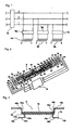
- Figure 1 is an oblique explanatory view showing the basic constitution of one example of a filament lamp in accordance with invention.
- Figure 2 is an elevational side view of the constitution of a filament assembly in accordance with the invention.
- Figure 3 is an enlarged view showing the connection of the lead and filament of the filament assembly.
- Figure 4 is a schematic representation of an example of the wiring connection between each filament and the power supply device.
- Figure 5 is a schematic representation of an example of the wiring connection between each filament and the power supply device that supplies three-phase alternating current power to each of multiple filaments.
- Figure 6 is an oblique explanatory view showing the basic constitution of another example of a filament lamp of the invention.
- Figure 7 is a schematic representation of an example of the wiring connection between each filament and the power supply device of the filament lamp shown in Figure 6.
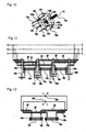
- Figure 8 is an oblique explanatory view showing an outline of the constitution of yet another filament lamp in accordance with the invention.
- Figure 9 is a side elevational view of the filament assembly of the filament lamp shown in Figure 8.
- Figure 10 is a perspective view of the connection between the filament assembly and a support part.
- Figure 11 is an explanatory view showing an example of the wiring connection between each filament and the power supply device of the filament lamp shown in Figure 8.
- Figure 12 is an explanatory view showing an example of the wiring connection between each filament and the power supply device of the filament lamp when the power supply used supplies direct current power to each of multiple filament assemblies.
- Figure 13 is a cross-sectional view showing the configuration of one example of the light-irradiation-type heat treatment device of this invention.
- Figure 14 is a plan view showing the array of filaments in a first lamp unit and a second lamp unit that make up the light source of the light-irradiation-type heat treatment device shown in Figure 13.
- Figure 1 is an oblique explanatory view showing an outline of the constitution of one example of the filament lamp of this invention.
- the filament lamp has a straight-line light emitting bulb 11 sealed at both ends, and within the light emitting bulb 11 are multiple (two are shown in Figure 1) filament assemblies 14, 15, comprising filament coils and leads that supply electricity to the filament coils, that are orderly arranged so that the filament coils 14b, 15b extend in the axial direction of the light emitting bulb 11.
- a lead 14c is connected to one end of the filament coil 14b and is electrically connected to an external lead 18a that projects through a sealed portion 12a of the light emitting bulb 11, by way of a metal foil 13a sealed within the sealed portion 12a, and another lead 14a is connected to the other end of the filament coil 14b and is electrically connected to an external lead 18d that projects through the other sealed portion 12b of the light emitting bulb 11, by way of a metal foil 13d sealed within the sealed portion 12b.
- a lead 15c is connected to one end of the filament coil 15b and is electrically connected to an external lead 18b by way of a metal foil 13b sealed within the sealed portion 12a
- another lead 15a is connected to the other end of the filament coil 15b and is electrically connected to an external lead 18c by way of a metal foil 13c sealed within the sealed portion 12b.
- the filament assemblies 14, 15 are connected by way of their respective external leads to separate power supply equipment, by which power can be supplied individually to the filaments 14b, 15b of the filament assemblies 14, 15.
- a circular anchor 17 is set along the axial direction of the light emitting bulb 11 in a position between the inner wall of the light emitting bulb 11 and the insulating tube 25.
- Each filament 14b, 15b is supported by, for example, three anchors 17 so that it does not contact the light emitting bulb 11.
- the filament lamp 10 has a straight-line light emitting bulb 11 made of a light-transparent material, such as quartz glass, and is formed with both ends fused into sealed parts 12a, 12b. Within this light emitting bulb 11, multiple -for example, two- filament assemblies 14, 15 are arranged sequentially in the axial direction of the light emitting bulb 11; a halogen gas and a specified discharge-suppressing gas described below are sealed within bulb 11.
- a halogen gas and a specified discharge-suppressing gas described below are sealed within bulb 11.
- the first filament assembly 14 comprises a filament coil 14b, a power supply lead 14a connected to the other end of the filament coil 14b, and a lead 14c connected to one end of the filament coil 14b.
- the lead 14a of the first filament assembly 14 is formed of a single strand of wire and comprises a coiled filament connector 141a that extends parallel to the coil axis of filament 14b with which it connects a radial direction part 143a that is continuous with the filament connector 141 a and extends in the radial direction from the filament connector 141 a, and a straight lead body 142a that is continuous with the radial direction part 143a and extends in the axial direction of the coil of the filament connector 141 a.
- the filament connector part 141 a has an outside diameter matching the inside coil diameter of the filament coil 14b.
- the lead 14c of the first filament assembly 14 has the same constitution as the lead 14a, with the symbols labeling each part changed for convenience to a "c" from the "a" of the constituent parts of the lead 14a.
- the radial direction part 143a of the lead 14a is screwed into the other end of the filament coil 14b, so that the filament connector 141 a is inserted into the inside space of the other end of the filament coil 14b and is positioned with its outer surface in contact with the inner surface of the filament coil 14b.
- the radial direction part 143a is sandwiched within the coil pitch of the filament coil 14b so that it projects outward in the radial direction of the filament coil 14b, by which a connection between the lead 14a and the filament coil 14b is achieved.
- the filament connector 141 c is positioned in contact with the inner surface of the filament coil 14b, and the radial direction part 143c is sandwiched within the coil pitch of the filament coil 14b so that it projects outward in the radial direction of the filament coil 14b, by which a connection between the lead 14c and the filament coil 14b is achieved.
- the second filament assembly 15 has the same constitution as the first filament assembly 14, and comprises a filament coil 15b, a power supply lead 15a connected to the other end of the filament coil 15b, and a lead 15c connected to one end of the filament coil 15b.
- the lead 14a at the other end of the first filament 14 is electrically connected to an external lead 18d by way of a metal foil 13d that is sealed within the sealed part 12b at the other end of the light emitting bulb 11. Further, the lead 14c at one end extends along the bulb axis of the light emitting bulb 11 so that it does not contact the second filament assembly 15, and is electrically connected to the external lead 18a by way of a metal foil 13a that is sealed within the sealed part 12a at one end of the light emitting bulb 11.
- the lead 15a at the other end of the second filament 15 extends along the bulb axis of the light emitting bulb 11 so that it does not contact the first filament assembly 14, and is electrically connected to the external lead 18c by way of a metal foil 13c that is sealed within the sealed part 12b at one end of the light emitting bulb 11. Further, the lead 15c is electrically connected at one end to the external lead 18b by way of a metal foil 13b that is sealed within the sealed part 12a at one end of the light emitting bulb 11.
- this filament lamp 10 there are insulating tubes made of an insulating material, such as quartz, in places where the lead of a filament assembly is opposite the filament or lead of the other filament assembly.
- insulating tubes made of an insulating material, such as quartz, in places where the lead of a filament assembly is opposite the filament or lead of the other filament assembly.
- an insulating tube 25 is placed on lead 14c at one end of the first filament assembly 14 where it is opposite the filament coil 15b of the second filament assembly 15, and an insulating tube 25 is placed on lead 15a at the other end of the second filament assembly 15 where it is opposite the filament coil 14b of the second filament assembly 14.
- each of the filament coils 14, 15 are supported by, for example, three anchors so that they do not contact the light-emission bulb 11.
- the anchors 17 are flexible to the extent that multiple filament assemblies can be easily inserted and positioned in the light emitting bulb 11 during the manufacture of the filament lamp 10.
- each of the external leads of the filament assemblies 14, 15 is electrically connected by power supply wiring to power supply device 73 that supplies, for example, single-phase alternating current power so that there will be the same phase at the adjacent ends of the first filament assembly 14 and the second filament assembly 15.
- one end of the filament coil 14b of the first filament assembly 14 is electrically connected by way of a power control means 74a to the high-voltage side (H) of the power supply device 73, and the other end is electrically connected by way of the power control means 74a to the ground (G), which is the low-voltage side (L) of the power supply device 73.
- filament coil 15b of second filament assembly 15 which is adjacent to one end of the first filament coil 14b is electrically connected, by way of the power control means 74b, to the high-voltage side H of the power supply device 73, and the lead 15c at one end is electrically connected, by way of the power control means 74b, to the ground side G. Consequently, the filament coils 14b, 15b are individually supplied power by way of the power control means 74a, 74b, and so the light emission of the filament coils 14b, 15b can be controlled individually.
- Thyristors SCR for example, can be used as the power control means 74a, 74b in this filament lamp 10, and it is possible to adjust the amount of current fed to the filament assemblies 14, 15 in a range from 0 to 100 % of the maximum rated current value of the filament coils 14b, 15b.
- a discharge-suppressing gas with a high dielectric break-down voltage value to which is added a halogen gas to use the halogen cycle, is sealed within the light emitting bulb 11 in the filament lamp 10 described above.
- nitrogen gas for example, nitrogen gas, a rare gas such as argon or krypton, or a mixture of nitrogen and a rare gas; of these, nitrogen gas is particularly preferable because it has a higher dielectric break-down voltage value than the other gases.
- the amount of rare gas sealed in is preferably in the range of about 0.8 x 10 5 to 1 x 10 6 Pa at normal temperature.
- the one end of filament coil 14b of the first filament assembly 14 and the other end of the filament coil 15b of the second filament assembly 15 will have the same electrical potential.
- a filament lamp 10 with the constitution described above, it is possible to independently control the state of light emission of the filaments 14b, 15b, and so it is possible to reliably obtain the desired distribution of luminance. Moreover, because alternating current power can be supplied so that the adjacent ends of the first filament assembly 14 and the second filament assembly 15 are in the same phase, the difference of electrical potential between them will be slight or zero, and so it is possible to reliably prevent the occurrence of unwanted discharge between the filaments 14b, 15b or between the neighboring leads 14c, 15a. As a result, it is possible to reliably prevent occurrence of the defect of melt-through of a filament coil or lead.
- the filament connectors 141a, 141c of leads 14a, 14c are positioned in a state of contact by insertion into the internal space of the filament coil 14b and the filament coil 14b and the leads 14a, 14c are connected with the radial direction parts 143a, 143c sandwiched in the coil pitch. Displacement in the axial direction of the filament coil 14b and displacement in the radial direction are controlled by this means, and so even in the event of connection between leads 14a, 14c and a filament coil 14b that has a large wire diameter and a large coil diameter, the two can be reliable connected without enlarging the wire diameter of the leads 14a, 14c to match the inside diameter of the filament coil 14b.
- the filament coil has a wire diameter of 0.5 mm and a coil winding diameter of 4.3 mm and the lead has a wire diameter of 0.8 mm, the two can be reliably connected. Further, the same applies to the second filament assembly 15.
- the filament lamp 10 it is possible to use a power supply device 75 that supplies three-phase alternating current power.
- the power supply device 75 has three terminals R, S, and T with mutually differing electrical potential, and each of the filaments 14b, 15b is electrically connected to two of these terminals in such a way that the adjacent ends of the first filament assembly 14 and the second filament assembly 15 are in the same phase.
- one end of the filament coil 14b of the first filament assembly 14 is electrically connected, by way of the power control means 74a, to the S terminal of the power supply device 75, and the other end is electrically connected, by way of the power control means 74a, to the R terminal of the power supply device 75.
- the other end of the filament coil 15b of the second filament assembly 15 that is adjacent to the one end of the first filament coil 14b is electrically connected, by way of the power control means 74b, to the S terminal of the power supply device 75, and the one end is electrically connected, by way of the power control means 74b, to the T terminal of the power supply device 75.
- the filament coil 14b of the first filament assembly 14 is connected to the R-S phase and the filament coil 15b of the second filament assembly 15 is connected to the S-T phase, by which means power is supplied individually to the filament coils 14b, 15b, by way of the power control means 74a, 74b, making it possible to individually control the state of light emission of the filament coils 14b, 15b.
- a filament lamp with this sort of constitution it is possible to obtain the same results as described above, and by using power supply device 75 that supplies three-phase alternating current power, it is possible to make a dispersed connection of a number of filaments electrically connected to each phase. And so, the current flowing in one phase can be less than that in the case of a single phase and the current required of the power supply device can be relatively low, so that the cost of supplying power can be reduced.
- the number of filaments can be changed appropriately in accordance with the purpose; as shown in Figure 6, for example, it is possible to have a constitution with an arrangement of three filament assemblies 14, 15, 16.
- This filament lamp 10 has a straight-line light emitting bulb 11 made of a light-transparent material such as quartz glass and formed with both ends fused into sealed parts 12a, 12b. Within this light emitting bulb 11 there are three filament assemblies 14, 15, 16, having the same constitution as that shown in Figure 2, with their filament coils sequentially arranged in the axial direction of the light emitting bulb 11.
- the leads 14c, 15c, 16c at one end of the first filament assembly 14, the second filament assembly 15, and the filament assembly 16 are electrically connected, by way of the metal foils 13d, 13e, 13f which are sealed within the sealed portions at one end, to external leads 18d, 18e, 18f, and the leads 14a, 15a, 16a at the other end are electrically connected, by way of the metal foils 13a, 13b, 13c which are sealed within the sealed portions at the other end, to external leads 18a, 18b, 18c.
- the external leads of the filament assemblies 14, 15, 16 are electrically connected by power supply wiring to the power supply device 75 so that the adjacent ends of the first filament assembly 14 and the second filament assembly 15 are in the same phase and the adjacent ends of the second filament assembly 15 and the third filament assembly 16 are in the same phase.
- one end of the filament coil 14b of the first filament assembly 14 is electrically connected, by way of the power control means 74a, to the S terminal of the power supply device 75, and the other end is electrically connected, by way of the power control means 74a, to the R terminal of the power supply device 75.
- one end of the filament coil 15b of the second filament assembly 15 is electrically connected, by way of the power control means 74b, to the S terminal of the power supply device 75, and the one end is electrically connected, by way of the power control means 74b, to the T terminal of the power supply device 75.
- one end of the filament coil 16b of the third filament assembly 16 is electrically connected, by way of the power control means 74c, to the R terminal of the power supply device 75, and the other end is electrically connected, by way of the power control means 74b, to the T terminal of the power supply device 75.
- the filament coil 14b of the first filament assembly 14 is connected to the R-S phase
- the filament coil 15b of the second filament assembly 15 is connected to the S-T phase
- the filament coil 16b of the third filament assembly 16 is connected to the T-R phase, by which means power is supplied individually to the filament coils 14b, 15b, 16b, by way of the power control means 74a, 74b, 74c, making it possible to individually control the state of light emission of the filament coils 14b, 15b, 16b.
- a discharge-suppressing gas with a high dielectric break-down voltage value to which is added a halogen gas to use the halogen cycle, be sealed within the light emitting bulb 11.
- the difference of electrical potential between one end of the filament coil 14b or lead of the first filament assembly 14 and the other end of the filament coil 15b or lead of the second filament assembly 15 is slight or non-existent, and the difference of electrical potential between one end of the filament coil 15b or lead of the second filament assembly 15 and the other end of the filament coil 16b or lead of the third filament assembly 16 is slight or non-existent.
- a filament lamp 10 with the constitution described above, it is possible to control independently the state of light emission of the filaments 14b, 15b, 16b, and so it is possible to reliably obtain the desired distribution of luminance. Moreover, because three-phase alternating current power can be supplied so that the adjacent ends of the filament assemblies are in the same phase, the difference of electrical potential between them will be slight or zero, and so it is possible to reliably prevent the occurrence of unwanted discharge between the neighboring filaments or between the neighboring leads. As a result, it is possible to reliably prevent occurrence of the defect of melt-through of a filament coil or lead.
- the discharge-suppressing gas will have a high dielectric break-down and it is possible to prevent, even more reliably, the occurrence of unwanted discharge caused by that difference of electrical potential. Accordingly, it is possible to reliably obtain the desired distribution of irradiation.
- the filament lamp of this invention the constitution shown in Figure 8 in which the filament lamp 10 has the same constitution as the filament lamp shown in Figure 6, except that the constitution of the filament assemblies is different from the filament lamp constitution shown in Figure 6, and multiple flat support pieces 19a, 19b, 19c, 19d made of an insulating material, such as quartz glass, are located within the light emitting bulb 11 in positions between the adjacent filaments and perpendicular to the bulb axis.
- the first filament assembly 14 comprises the filament coil 14b, a power supply lead 14a connected to the other end of this filament coil 14b, and a lead 14c connected to the one end of the filament coil 14b.
- the lead 14a at the other end of the filament coil 14b is formed of a single strand of wire and has a wire lead body 142a and a hook-shaped portion 140a with a radial direction part that extends in a direction perpendicular to the lead body 142 (the radial direction of the connected filament coil).
- the hook-shaped portion 140a comprises a radial direction part 143a that is continuous with the lead body 142a and is bent to extend in a direction perpendicular to the lead body 142a, a coiled filament connector 141a that is continuous with the radial direction part 143a and that extends with its coil axis parallel to the lead body 142a, and an L-shaped part 144a that is continuous with the filament connector 141a, extends in a direction perpendicular to the direction of the coil axis, and is bent so the tip extends in the direction of the coil axis.
- the filament connector 141a has an outside diameter that matches the inside coil diameter of the filament coil 14b.
- the tip of the L-shaped part 144a of the lead 14a has an edgeless globular part 145a formed by melting with, for example, a laser.
- the lead 14c at the one end of the first filament assembly 14 has the same constitution as the lead 14a, with the symbols labeling each part changed for convenience to a "c" from the "a" of the constituent parts of the lead 14a.
- first filament assembly 14 by twisting the other end of the filament coil 14b onto the L-shaped 144a of the lead 14a, the filament connector 141 a can be inserted in the internal space in the other end of the filament coil 14b and positioned with its outer surface in contact with the inner surface of the filament coil 14b; the L-shaped part 144a will be sandwiched within the coil pitch of the filament coil 14b and will project outward in the radial direction of the filament coil 14b, by which means the connection of the lead 14a and the filament coil 14b is achieved.
- the filament connector 141c is positioned with its outer surface in contact with the inner surface of the filament coil 14b; the L-shaped part 144c is sandwiched within the coil pitch of the filament coil 14b and projects outward in the radial direction of the filament coil 14b, by which means the connection of the lead 14c and the filament coil 14b is achieved.
- the second filament assembly 15 and the third filament assembly 16 have the same constitution as the first filament assembly 14, with the power supply lead 15a (16a) connected to the other end of the filament coil 15b (16b) and the lead 15c (16c) connected to the one end of the filament coil 15b (16b).
- an opening 197 is formed roughly in the center of the support piece 19a, and multiple, perhaps six, cut-outs 191, 192, 193, 194, 195, 196, that constitute a positioning mechanism to determine the position of the filaments are formed at equidistant positions on the periphery.
- Forming the opening 197 is not essential, but making the opening 197 in the support piece enables enlargement of the gap between the support piece and the filament coil and makes it possible to reduce the thermal load on the support piece.
- the other support pieces 19b, 19c, 19d are constituted in the same way as the support piece 19a.
- the first filament assembly 14 is attached to the support piece 19a by engaging the L-shaped part 144a of the lead 14a on the other end in the cut-out 196 of the support piece 19a and inserting the lead body 142a into the opposite cut-out 193, with the filament coil 14b extending from the support piece 19a in a direction perpendicular to one face of the support piece 19a.
- the lead 14c at the one end is similarly attached to the support piece 19b by engaging the L-shaped part 144c of the lead 14c on the one end in a cut-out of the support piece 19b and inserting the lead body 142c into the opposite cut-out, with the filament coil 14b extending from the support piece 19b in a direction perpendicular to the other face of the support piece 19b.
- the lead 14a at the other end of the first filament assembly 14 is electrically connected, by way of the metal foil 13a sealed within the sealed portion 12a at the other end of the light emitting bulb 11, to the external lead 18a.
- the lead 14c at one end is inserted into cut-outs in support pieces 19c, 19d not used for determining the positions of the hook-shaped parts of the leads of the second filament assembly 15 and the third filament assembly 16, and extends along the bulb axis of the light emitting bulb 11; it is electrically connected, by way of the metal foil 13d sealed within the sealed portion 12b at the one end of the light emitting bulb 11, to the external lead 18d.
- the second filament assembly 15 is attached to the support piece 19b by engaging the hook-shaped part of the lead 15a on the other end in a cut-out of the support piece 19b not used for determining the position of the lead 14c of the first filament assembly 14 and inserting the lead body 152a into the opposite cut-out, with the filament coil 15b extending from the support piece 19b in a direction perpendicular to one face of the support piece 19b.
- the hook-shaped part of the lead 15c at one end is attached to the support piece 19c in the same way, by which means the second filament assembly 15 is positioned and supported in the light emitting bulb 11.
- the lead 15a at other end of the second filament assembly 15 is inserted into the cut-out 191 in support piece 19a, which is not used for determining the positions of the lead 14a of the first filament assembly 14 (see Figure 10), and extends along the bulb axis of the light emitting bulb 11.
- the lead 15a is electrically connected, by way of the metal foil 13b sealed within the sealed portion 12a at the other end of the light emitting bulb 11, to the external lead 18b.
- the lead 15c at one end is inserted into a cut-out in the support piece 19d that is not used for determining the positions of the lead 16c of the third filament assembly 16, and extends along the bulb axis of the light emitting bulb 11.
- the lead 15c is electrically connected, by way of the metal foil 13e sealed within the sealed portion 12b at the one end of the light emitting bulb 11, to the external lead 18e.
- the third filament assembly 16 is attached to the support piece 19c by engaging the hook-shaped part of the lead 16a on the other end in a remaining cut-out of the support piece 19b that supports the second filament assembly 15 and inserting the lead body into the opposite cut-out, with the filament coil 16b extending from the support piece 19c in a direction perpendicular to one face of the support piece 19c.
- the hook-shaped part of the lead 16c at one end is attached to the support piece 19d in the same way, by which means the third filament assembly 16 is positioned and supported in the light emitting bulb 11.
- the lead 16a at the other end of the third filament assembly 16 is inserted into cut-outs in support pieces 19b, 19a that are not used for determining the positions of the leads 14a, 14c, 15a of the other filament assemblies 14, 15 (for example, cut-out 195 in support piece 19a; see Figure 10), and extends along the bulb axis of the light emitting bulb 11.
- the lead 16a is electrically connected, by way of the metal foil 13c sealed within the sealed portion 12a at the other end of the light emitting bulb 11, to the external lead 18c.
- the lead 16c at one end of the filament assembly 16 is electrically connected, by way of the metal foil 13f sealed within the sealed portion 12b at the one end of the light emitting bulb 11, to the external lead 18f.
- the external leads of the filament assemblies 14, 15, 16 are electrically connected by power supply wiring to the power supply device 75, which supplies three-phase alternating current power, in such a way that the adjacent ends of the first filament assembly 14 and the second filament assembly 15 are in the same phase and the adjacent ends of the second filament assembly 15 and the third filament assembly 16 are in the same phase.
- the filament coil 14b of the first filament assembly 14 is connected in the R-S phase
- the filament coil 15b of the second filament assembly 15 is connected in the S-T phase
- the filament coil 16b of the third filament assembly 16 is connected in the T-R phase, by which means the filament coils 14b, 15b, 16b are individually supplied power by way of a power control means (not illustrated), making it possible to individually control the state of light emission of the filament coils 14b, 15b, 16b.
- a filament lamp 10 with the constitution described above, it is possible to obtain the same results as with the filament lamp 10 described above. That is, it is possible to control independently the state of light emission of the filaments 14b, 15b, 16b, and so it is possible to reliably obtain the desired distribution of luminance. Moreover, because three-phase alternating current power can be supplied so that the adjacent ends of the filament assemblies are in the same phase, the difference of electrical potential between them will be slight or zero, and so it is possible to reliably prevent the occurrence of unwanted discharge between the neighboring filaments or between the neighboring leads. As a result, it is possible to reliably prevent occurrence of the defect of melt-through of a filament coil or lead.
- the discharge-suppressing gas will have a high dielectric break-down and it is possible to prevent, even more reliably, the occurrence of unwanted discharge caused by that difference of electrical potential. Accordingly, it is possible to reliably obtain the desired distribution of irradiation.
- the leads of the filament assemblies are supported by support pieces that form a positioning mechanism by engaging the hook-shaped portions in the cut-outs, by which means displacement (movement) of the filament coil in the peripheral direction is controlled, and so position determining of the filament assemblies can be made even more reliable.
- the filament coils 14b, 15b, 16b can be precisely and easily positioned in its desired position in the light emitting bulb 11, and changes in the position of the filament assembly over time can be prevented so that it is possible to reliably maintain the initial performance over a long period.
- Figure 12 is an explanatory view showing one example of the wiring connection between each filament and the power supply device in another embodiment of the filament lamp of this invention.
- the lead 14c at one end of the first filament assembly 14 is connected to the high-voltage side (positive electrode side) of the first direct current power supply 78a
- the lead 14a at the other end of the first filament assembly 14 is connected to the low-voltage side (negative electrode side) of the first direct current power supply 78a.
- the lead 15c at one end of the second filament assembly 15 is connected to the high-voltage side (positive electrode side) of the second direct current power supply 78b, and the lead 15a at the other end of the second filament assembly 15 is connected to the low-voltage side (negative electrode side) of the second direct current power supply 78b.
- the adjacent ends of the first filament assembly 14 and the second filament assembly 15 have the same polarity, and the direct current power supply devices 78a, 78b invests direct current power separately in the filament coils 14b, 15b.
- a filament lamp constituted as described above provides the same results as a constitution in which alternating current power is supplied to the filament assemblies. That is, because direct current power is supplied so that the adjacent ends of the first filament assembly 14 and the second filament assembly 15 have the same polarity, even in the event that a large amount of power is supplied to the filaments, the difference in electrical potential between them will be slight or zero, and so it is possible to reliably prevent the occurrence of unwanted discharge between the filament coils 14b, 15b or between the leads 14c, 15c. As a result, it is possible to reliably prevent the occurrence of the defect of filament or lead melt-through.
- a discharge-suppressing gas is sealed within the light emitting bulb, and since the discharge-suppressing gas has a high dielectric break-down, it is possible to prevent, even more reliably, the occurrence of unwanted discharge.
- the number of filament assemblies is not limited, and can be changed as is appropriate to the purpose. If there is a large number of filament assemblies, it is possible to control the distribution of luminance relative to the article to be treated even more precisely. For a diffusion process that requires highly precise temperature control, for example, five or more are preferable, and in the event of treatment of large semiconductor wafers of a diameter of 300 mm or more, seven to nine are preferable.
- the conductive material fused into the sealed portions is not limited to metal foil; a plate-shaped piece can be used.
- the filament lamp of this invention is constituted to enable independent control of the state of light emission of multiple filaments arranged within the light emitting bulb, and it is constituted to enable investment of large amounts of power into the filament assemblies without causing unwanted discharge between the filament assemblies. It is, therefore, very useful as a heating light source for light-irradiation-type heat treatment.
- the light-irradiation-type heat treatment device of this invention is explained below.
- Figure 13 is a front cross-sectional view showing an outline of the constitution of one example of the light-irradiation-type heat treatment device of this invention.
- Figure 14 is a plane view showing the array of filaments in the first lamp unit and the second lamp unit that make up the light source of the light-irradiation-type heat treatment device shown in Figure 13.
- This light-irradiation-type heat treatment device 100 has a chamber 300 of which the interior space is divided vertically by an aperture plate 4 made of quartz, for example, forming a lamp unit accommodation space S 1 and a heat treatment space S2.
- a first lamp unit 200A having perhaps ten of the filament lamps 10 described above positioned with their central lamp axes in one plane and parallel at a specified distance and a second lamp unit 200B having perhaps ten of the filament lamps 10 described above positioned with their central lamp axes in one plane and parallel at a specified distance are arranged opposite each other, one above and one below.
- the filament lamps 10 of the first lamp unit 200A and the filament lamps 10 of the second lamp unit 200B have their central lamp axial directions crossing each other.
- a reflecting mirror 201 that reflects the light beams irradiated upward from the first lamp unit 200A and the second lamp unit 200B onto the article to be treated W is located above the first lamp unit 200A.
- the reflecting mirror 201 is, for example, gold coated onto a base of oxygen-free copper, and the reflecting cross section has a shape selected from, for example, part of a circle, part of an ellipse, part of a parabola, or flat.
- the filament lamps 10 of the first lamp unit 200A are supported by a pair of first fixed beds 650, 651.
- the first fixed beds 650, 651 comprise conductive beds 66 made of a conductive material and support beds 67 made of a ceramic or other insulating material.
- the support beds 67 are mounted on the wall of the chamber 300 and support the conductive beds 66.
- n1 x m1 sets of paired first fixed beds 650, 651 will be required for a constitution that supplies power independently to all the filament assemblies.
- the filament lamps 10 of the second lamp unit 200B are supported by second fixed beds (not shown); the second fixed beds, like the first fixed beds, comprise conductive beds and support beds.
- n2 x m2 sets of paired second fixed beds will be required for a constitution that supplies power independently to all the filament assemblies.
- Paired power source supply ports 71, 72 that are connected to the power supply wiring from the multiple power supply devices that make up a power source 7 are located in the chamber 300; the number of sets of paired power source supply ports 71, 72 is set in accordance with the number of filament lamps 10 and the number of filament assemblies in each filament lamp 10.
- the power source supply ports 71 are electrically connected to the conductive beds 66 of the first lamp fixed beds 650 and the conductive beds 66 of the first lamp fixed beds 650 are electrically connected to, for example, the external leads that are connected to the leads 14a connected to the other ends of the filament coils 14b.
- the power source supply ports 72 are electrically connected to the conductive beds 66 of the first lamp fixed beds 651 and the conductive beds 66 of the first lamp fixed beds 651 are electrically connected to, for example, the external leads that are connected to the leads 14c connected to the one ends of the filament coils 14b.
- the filament coils 14b of one filament lamp in the first lamp unit 200A are electrically connected to the power supply device 7a of the power source 7.
- the other filament coils 15b, 16b in this filament lamp 10 are electrically connected in the same way to power supply devices by other paired power source supply ports 71, 72. Then, the same electrical connections to power supply devices are made for the filament coils of other filament lamps 10 making up the first lamp unit 200A and the filament coils of the filament lamps 10 making up the second lamp unit 200B.
- the distribution of luminance on the article to be treated W can be set at will and with high precision by selectively lighting the filament coils or by individually regulating the amount of power supplied to each filament coil.
- a cooling mechanism to cool the filament lamps during heat treatment of the article to be treated W is installed in this light-irradiation-type heat treatment device.
- cooling air from a cooling air unit 8 mounted outside the chamber 300 is introduced into the lamp unit accommodation space S1 by way of the jet 82 of a cooling air supply nozzle 81, and by blowing this cooling air onto the filament lamps in the first lamp unit 200A and the second lamp unit 200B, the light emitting bulbs 11 that make up each filament lamp 10 are cooled, after which cooling air that has attained a high temperature through heat exchange is exhausted to the outside through a cooling air exhaust port 83 formed in the chamber 300.
- the jets 82 of the cooling air supply nozzles 81 of this cooling mechanism be formed pointing at the sealed parts 12a, 12b of the filament lamps so as to preferentially cool the sealed parts 12a, 12b of the filament lamps.
- the flow of the cooling air introduced into the lamp unit accommodation space S1 is set so that cooling air that has attained a high temperature through heat exchange does not heat the filament lamps instead, and so that the reflecting mirror 201 is cooled simultaneously. Further, it is not necessary to set the flow of cooling air so the reflecting mirror 201 will be cooled simultaneously if the reflecting mirror 201 is constituted with water cooling by means of a water cooling mechanism (not shown).
- this light-irradiation-type heat treatment device 100 is constituted with jets 82 of the cooling air supply nozzles 81 positioned near the aperture plate 4 so the aperture plate 4 is cooled by cooling air from the cooling air unit 8.
- the treatment support 5 is a thin, ring-shaped body made of a high melting point metallic material, such as molybdenum, tungsten, or tantalum, of a ceramic material, such as silicon carbide (SiC), or of quartz or silicon (Si).
- the treatment support 5 is preferably constructed with a guard ring structure formed with steps to support the semiconductor wafer within a circular opening.
- the treatment support 5 itself is raised to a high temperature by the light irradiation, the treatment support 5 provides supplemental thermal radiation to the opposing edge of the semiconductor wafer, and thus compensates for reduced temperatures at the edge of the semiconductor wafer caused by such things as thermal radiation from the edge of the semiconductor wafer.
- thermocouples or radiation thermometers are placed behind the article to be treated W that is set on the treatment support 5, in contact with or close to the article to be treated W, and the temperature gauges 91 are connected to a thermometer 9.
- the temperature gauges 91 are connected to a thermometer 9.
- the thermometer 9 Based on the temperature information monitored by the temperature gauges 91, the thermometer 9 has the functions of calculating the temperatures at the measurement points of the temperature gauges 91, based on the temperature information monitored by the temperature gauges 91, and sending the calculated temperature information to the main controller 3 by way of the temperature controller 92.
- the main controller 3 has the function of sending commands to the temperature controller 92, based on the temperature information at the measurement points on the article to be treated W, so that the temperatures on the article to be treated W will be at the specified level and distributed uniformly.
- the temperature controller 92 has the function of controlling, on the basis of commands from the main controller 3, the amounts of power supplied to the filament coils of the filament lamps from the power source 7.
- the main controller receives temperature information from the temperature controller to the effect that the temperature at a measurement point is lower than the designated temperature, it sends a command to the temperature controller 92 to increase the amount of power supplied to the filament coils that provide light-irradiation to the measurement point in question and nearby positions, so that the light radiated from those filament coils will be increased.
- the temperature controller 92 increases the power supplied from the power source 7 to the power source supply ports 71, 72 connected to the filament coils in question.
- the main controller 3 also sends commands to the cooling air unit 8 when the filament lamps 10 in the lamp units 200A, 200B are burning, and based on those commands, the cooling air unit 8 provides cooling air so that the light emitting bulbs 11, the reflecting mirror 201, and the aperture plate 4 do not overheat.
- a process gas unit which introduces and exhausts process gases to and from the heat treatment space S2 in accordance with the variety of heat treatment, is connected to this light-irradiation-type heat treatment device.
- a process gas unit 800 is connected to introduce and exhaust oxygen gas to the heat treatment space S2, and to introduce a purge gas (such as nitrogen gas) to purge the heat treatment space S2 and exhaust it.
- a purge gas such as nitrogen gas
- the process gas and purge gas from the process gas unit 800 are introduced into the heat treatment space S2 by way of jets 85 of gas supply nozzles 84 installed in the chamber 300, and are exhausted to the outside by way of exhaust ports 86.
- the filament coils of the filament lamps making up the first lamp unit 200A and the second lamp unit 200B are lit by supplying power controlled at the proper level to them from the power source 7; by this means the light radiated by the filament lamps irradiates the article to be treated W mounted in the heat treatment space S2 through the aperture plate 4, either directly or reflected by the reflecting mirror 201, and heat treatment of the article to be treated W is performed.
- the filament lamps that make up the first lamp unit 200A and the second lamp unit 200B are constituted to prevent unwanted discharge between the adjacent parts of neighboring filament assemblies, and so in both the first lamp unit 200A and the second lamp unit 200B, filament lamps 10 that have multiple filament assemblies orderly arranged lengthwise in the light emitting bulb, power being supplied to each filament assembly independently, are arranged in rows.
- region 1 the temperature of the region beneath the points where filament lamp 10A crosses filament lamps 10B, 10C
- region 2 the temperature of the rest of the article to be treated W
- region 1 the temperature of the region beneath the points where filament lamp 10A crosses filament lamps 10B, 10C
- region 2 the temperature of the rest of the article to be treated W
- the lines drawn within the individual filament lamps in Figure 14 indicate the positions of filament coils. It is possible, therefore, to perform heat treatment with a temperature distribution that is uniform across the entire article to be treated W.
- the positions of filament coils in each filament lamp 10 is shown with a single straight line in Figure 14, but this indicates the total length of multiple, lined-up filament coils; depiction of the multiple filament coils one by one has been omitted.
- the filament lamp 10 is constituted so that undesired discharge between filaments can be reliably prevented and so that the separating distance between the filaments in the light emitting bulb is very small, it is possible to minimize the effect of the non-light-emitting gaps between filaments, and to hold unwanted scattering of the luminance distribution on the article to be treated to very low levels.
Abstract
Double hook shaped parts (140a,140c,142a,142c) support each filament in the common bulb (11).
Description
- This invention relates to a filament lamp and light-irradiation-type heat treatment device, and particularly, to a filament lamp used for heat treatment of an article and a light-irradiation-type heat treatment device equipped with such a filament lamp.
- Heat treatment is used in a variety of processes in the manufacture of semiconductors, including film growth, oxidation, implantation of impurities, nitriding, film stabilization, silicidation, crystallization, and ion injection activation. In particular, rapid thermal processing (hereafter RTP) of a semiconductor wafer or other article to be treated by quickly raising and lowering its temperature enables improved throughput and quality, and so its use is desirable.
Light-irradiation-type heat treatment devices that can heat the article to be treated without contacting it, by means of light irradiation from a light source, such as an incandescent lamp with filaments arranged inside a light emitting bulb made of a material that is transparent to light, is widely used as heat treatment device used for RTP (see,JP-A-H7-37833 JP-A-2002-203804 U.S. Patent 6,876,816 ). - By means of a light-irradiation-type heat treatment device of this type, it is possible to heat the article to be treated to a temperature of 1000 °C or higher in a period of from several seconds to several tens of seconds, and to cool the article quickly by stopping the light irradiation.
- When using a light-irradiation-type heat treatment device of this type to perform RTP of semiconductor wafers, for example, unevenness of the temperature distribution of a semiconductor wafer when it is heated to a temperature of 1050 °C or higher is liable to cause a phenomenon called "slip" in the semiconductor wafer, in which crystal transition defects arise and quality declines, and so it becomes necessary to heat the semiconductor wafer, hold it at a high temperature, and then cool it so that the temperature distribution will be even across the entire surface.
- Even in the event that the light irradiation is performed so that the degree of irradiation is even for semiconductor wafers that have the same treatment characteristics across the entire irradiated surface, at the edges of the semiconductor wafer, heat will be radiated by the side surfaces of the semiconductor wafer, and so the temperature at the edges of the semiconductor wafer will be reduced and there will be unevenness in the temperature distribution of the semiconductor wafer.
- To resolve problems of this sort, there have been attempts to make up for the temperature drop due to heat radiation from the sides of the semiconductor wafer, and thus, even out the temperature distribution in the semiconductor wafer by means of light irradiation of the surface at the edges of the semiconductor wafer to a greater degree than the surface at the center of the semiconductor wafer.
- However, there may be small, special regions in the article to be treated that are very small relative to the length of the emitted light of the incandescent lamp, and when light irradiation is performed at a light intensity appropriate to the characteristics of these special regions, the regions other than the special regions are irradiated under the same conditions, and so it has not been possible with earlier heat treatment device to adjust temperatures to provide suitable temperature conditions for both the special regions and the other regions, or in other words, to control only the degree of irradiation of the small, special regions so that the temperature status of the article to be treated will be even.
- For example, it is common to form a film of metallic oxide or other material on the surface of a semiconductor wafer by the sputtering method and then dope it with impurities by means of ion implantation; the film thickness of such a metallic oxide and the density of the impurity ions will have a localized distribution on the surface of the semiconductor wafer. This localized distribution will not necessarily have central symmetry with respect to the center of the semiconductor wafer; sometimes, with regard to the density of the impurity ions, for example, the density of the impurity ions varies in small, special regions that do not have central symmetry with respect to the center of the semiconductor wafer.
- Even in the event that light irradiation is performed so that there is the same degree of irradiation of such special regions and the other regions, there will be differences between them in the speed of temperature rise and the temperature in the special regions will not necessarily be the same as the temperature in other regions, and there may be the problem that the unwanted temperature distribution in the treatment temperature of the article being treated results in difficulty in giving the desired physical properties to the article being treated.
- In view of that situation, the present inventors proposed a filament lamp with the following constitution, to be used as the light source of a light-irradiation-type heat treatment device (see the specification of
Japanese patent application 2005-191222 U.S. Patent Application Publication 2006-197454 ). - A filament lamp with this constitution has multiple filaments in a light emitting bulb and is constituted to enable individual control of the light emitted by each filament, so that, if it is used as a light source for heating in a light-irradiation-type heat treatment device, it is possible to arrange filaments with high precision with respect to the regions to be irradiated on the article to be treated, by aligning the filaments in parallel rows. Accordingly, by means of such light-irradiation-type heat treatment device, it is possible to supply power individually to the multiple filaments and to individually control the light emitted by each filament, and so it is possible to irradiate with the desired irradiation distribution according to the characteristics of the article to be treated even when the distribution of localized temperature variations on the article to receive heat treatment is non-symmetrical with respect to the article to be treated, with the result that the article to be treated can be heated evenly and an even temperature distribution can be achieved across the entire irradiated surface of the article to be treated.
- In recent years, there have been demands for further improvement of throughput (improved processing efficiency) and quality in light-irradiation-type heat treatment devices. To meet these demands, it is considered necessary to further speed up the temperature rise characteristics of semiconductor wafers when filament lamps with the constitution described above are used as light sources; for example, it is considered possible to respond by supplying more power per unit length to the filament than in the past.
- However, it was judged that, if the power supplied to the filament is simply increased, there is liable to be unwanted discharge between the leads of neighboring filament assemblies. If such unwanted discharge continues over a long period, there will be the defect of the filament or the lead melting through.
- Further, as stated above, to make the temperature distribution even on the irradiated surface of the article to be treated, it is desirable that the filament assemblies be arranged so that the filaments are close to each other (with a small space between filaments), but the problem described above becomes marked with such a constitution.
- This invention is directed to solving of the above-indicated problems. In particular, it is a primary object of the present invention to provide a filament lamp that reliably enables the desired irradiation distribution and also reliably prevents unwanted discharge between filaments or leads of neighboring filament assemblies, thus reliably preventing damage to filaments and leads even when large amounts of power are supplied to the filaments.
- Further, another object of this invention is to provide a light-irradiation-type heat treatment apparatus that has such a filament lamp and that is able to evenly heat the article to be treated.
- These objects are achieved by a filament lamp as claimed in
claims 1 to 7 and by a light-irradiation-type heat treatment device as claimed in claim 8. - In accordance with the invention the filament lamp has multiple filament assemblies, each comprising a coiled filament and connected leads to supply power to that filament, within a straight-line light emitting bulb with a sealed portion at at least one end, the filament assemblies being orderly arranged in the axial direction of the light emitting bulb axis so that each filament extends in the direction of the bulb axis, the leads of each filament assembly being electrically connected to respective multiple conductive parts set in the sealed portions, and having a power supply mechanism that supplies power to each filament independently, in which the power supply mechanism is an alternating current power supply that is connected to the conductive parts and supplies in-phase current.
- The adjacent terminals of neighboring filament assemblies will preferably have the same electrical potential. Further, the power supply mechanism in the filament lamp of this invention can be one that supplies three-phase alternating current power to each filament assembly.
- Further, the filament lamp of this invention can also be one that has multiple filament assemblies, each comprising a coiled filament and connected leads to supply power to that filament, within a straight-line light emitting bulb with a sealed portion at at least one end, the filament assemblies being orderly arranged in the axial direction of the light emitting bulb axis so that each filament extends in the direction of the bulb axis, the leads of each filament assembly being electrically connected to the respective multiple conductive parts set in the sealed portions, and having a power supply mechanism that supplies power to each filament independently, in which the power supply mechanism is a direct current power supply that is connected to the conductive parts so that the adjacent terminals of neighboring filament assemblies will have the same polarity.
- A constitution in which a discharge suppressing gas is sealed within the light emitting bulb is desirable in the filament lamp of this invention.
- Further, the filament lamp of each filament assembly can have a hook-shaped part the tip of which has a radial-direction part that is sandwiched within the coil pitch of the filament and that extends outward in the radial direction of the filament coil. Each of the leads connected to the adjacent ends of neighboring filaments is supported by common support pieces formed of positioning mechanisms with which the hook-shaped parts are engaged, by which means the position of the filament in the light emitting bulb is fixed. Furthermore, globular parts are formed on the hook-shaped part tips that sandwich the support pieces and extend toward each other.
- The light-irradiation-type heat treatment device of this invention has a lamp unit with the multiple filament lamps as described above arranged in parallel, in which the article to be treated is heated by irradiating the article to be treated with light emitted by the light unit.
- By means of the filament lamp of the invention, it is basically possible to control the light emission of each filament independently, and so it is possible to reliably obtain the desired distribution of irradiation intensity and also to supply alternating current power of the same phase to the adjacent ends of neighboring filament assemblies, thus reducing or eliminating the difference of electric potential between them, and thereby making it possible to reliably prevent the melt-through of filaments or leads caused by the occurrence of unwanted discharge between neighboring filaments or between neighboring leads.
- Accordingly, it is possible to supply high power, e.g., 200 W/cm or more, to the filaments and thereby bring about rapid temperature rise characteristics in semiconductor wafers.
- According to a second feature of the invention, the power supply mechanism used is one that supplies three-phase alternating current power to the filament assembly so that dispersed connection of a number of filaments that are electrically connected in each phase is possible. The current value flowing in each phase will be smaller than in the case of a single phase and the current value required of the power supply device will be relatively small, so that a reduction of power supply costs is possible.
- According to another aspect of the invention, the filament lamp has multiple filament assemblies, each comprising a coiled filament and connected leads to supply power to that filament, within a straight-line light emitting bulb with a sealed portion at at least one end, the filament assemblies being orderly arranged in the axial direction of the light emitting bulb axis so that each filament extends in the direction of the bulb axis, the leads of each filament assembly being electrically connected to respective multiple conductive parts set in the sealed portions, and having a power supply mechanism that supplies power to each filament independently, in which the power supply mechanism is a direct current power supply that is connected to the conductive parts so that the adjacent terminals of neighboring filament assemblies will be in the same polarity. By this means, it is basically possible to control the light emission of each filament independently, and so it is possible to reliably obtain the desired irradiation distribution, and also to supply direct current power so that the adjacent ends of neighboring filament assemblies have the same polarity, thus reducing or eliminating the difference of electric potential between them, thereby making it possible to reliably prevent the melt-through of filaments or leads caused by the occurrence of unwanted discharge between neighboring filaments or between neighboring leads.
- By means of a discharge-suppressing gas being sealed within the light emitting bulb, according to another feature of the invention, even if a difference of electrical potential between the leads of neighboring filament assemblies occurs when the temperature in small regions of the article to be treated is adjusted by supplying current of differing magnitudes to individual filaments, the occurrence of unwanted discharge will be even more reliably prevented because of the high dielectric break-down voltage of the discharge-suppressing gas.
- According to another aspect of the invention, a globular part is formed on the tip of the hook-shaped portion of the lead so that discharge is concentrated at the end of the lead, and so it is possible to reliably prevent the occurrence of unwanted discharge between neighboring leads.
- Further, the hook-shaped portion of the lead is engaged with and supported by a support piece so that displacement with respect to the radial direction of the filament and displacement in the peripheral direction of the filament are regulated and the globular part is checked by the support piece so that movement in the axial direction of the filament assembly is controlled. Therefore, the filament position can be determined even more reliably, each filament can be precisely and easily positioned in its desired position in the light emitting bulb, and changes in the position of the filament assembly over time can be prevented so that it is possible to reliably maintain the initial performance over a long period.
- By means of the light-irradiation-type heat treatment device of this invention, having a lamp unit comprising multiple filament lamps makes it possible to set the illumination distribution on the article to be treated precisely and as desired when separated from the lamp unit at a given distance. Therefore, even when the distribution of localized temperature variations on the article to be treated is non-symmetrical with respect to the shape of the article to be treated, it is possible to set the illumination distribution on the article to be treated in response to that, and heat the article to be treated evenly.
- Moreover, because the filaments are constituted to enable investment of a large amount of power in the filaments, it is possible to further improve throughput and quality.
- Figure 1 is an oblique explanatory view showing the basic constitution of one example of a filament lamp in accordance with invention.
- Figure 2 is an elevational side view of the constitution of a filament assembly in accordance with the invention.
- Figure 3 is an enlarged view showing the connection of the lead and filament of the filament assembly.
- Figure 4 is a schematic representation of an example of the wiring connection between each filament and the power supply device.
- Figure 5 is a schematic representation of an example of the wiring connection between each filament and the power supply device that supplies three-phase alternating current power to each of multiple filaments.
- Figure 6 is an oblique explanatory view showing the basic constitution of another example of a filament lamp of the invention.
- Figure 7 is a schematic representation of an example of the wiring connection between each filament and the power supply device of the filament lamp shown in Figure 6.
- Figure 8 is an oblique explanatory view showing an outline of the constitution of yet another filament lamp in accordance with the invention.
- Figure 9 is a side elevational view of the filament assembly of the filament lamp shown in Figure 8.
- Figure 10 is a perspective view of the connection between the filament assembly and a support part.
- Figure 11 is an explanatory view showing an example of the wiring connection between each filament and the power supply device of the filament lamp shown in Figure 8.
- Figure 12 is an explanatory view showing an example of the wiring connection between each filament and the power supply device of the filament lamp when the power supply used supplies direct current power to each of multiple filament assemblies.
- Figure 13 is a cross-sectional view showing the configuration of one example of the light-irradiation-type heat treatment device of this invention.
- Figure 14 is a plan view showing the array of filaments in a first lamp unit and a second lamp unit that make up the light source of the light-irradiation-type heat treatment device shown in Figure 13.
- Figure 1 is an oblique explanatory view showing an outline of the constitution of one example of the filament lamp of this invention.
- With reference to Figure 1, the filament lamp has a straight-line
light emitting bulb 11 sealed at both ends, and within thelight emitting bulb 11 are multiple (two are shown in Figure 1)filament assemblies light emitting bulb 11. - In the
first filament assembly 14, a lead 14c is connected to one end of thefilament coil 14b and is electrically connected to anexternal lead 18a that projects through a sealed portion 12a of thelight emitting bulb 11, by way of ametal foil 13a sealed within the sealed portion 12a, and another lead 14a is connected to the other end of thefilament coil 14b and is electrically connected to an external lead 18d that projects through the other sealedportion 12b of thelight emitting bulb 11, by way of a metal foil 13d sealed within the sealedportion 12b. There is an insulatingtube 25 on the portion of the lead 14c that is opposite thefilament coil 15b of thesecond filament assembly 15. - Further, in the
second filament assembly 15, a lead 15c is connected to one end of thefilament coil 15b and is electrically connected to an external lead 18b by way of ametal foil 13b sealed within the sealed portion 12a, and another lead 15a is connected to the other end of thefilament coil 15b and is electrically connected to anexternal lead 18c by way of ametal foil 13c sealed within the sealedportion 12b. There is an insulatingtube 25 on the portion of thelead 15a that is opposite thefilament coil 14b of the onefilament assembly 14. - The
filament assemblies filaments filament assemblies - Further, a
circular anchor 17 is set along the axial direction of thelight emitting bulb 11 in a position between the inner wall of thelight emitting bulb 11 and the insulatingtube 25. Eachfilament anchors 17 so that it does not contact thelight emitting bulb 11. - The
filament lamp 10 has a straight-linelight emitting bulb 11 made of a light-transparent material, such as quartz glass, and is formed with both ends fused into sealedparts 12a, 12b. Within thislight emitting bulb 11, multiple -for example, two-filament assemblies light emitting bulb 11; a halogen gas and a specified discharge-suppressing gas described below are sealed withinbulb 11. - As shown in Figure 2, the
first filament assembly 14 comprises afilament coil 14b, apower supply lead 14a connected to the other end of thefilament coil 14b, and a lead 14c connected to one end of thefilament coil 14b. - The lead 14a of the
first filament assembly 14 is formed of a single strand of wire and comprises a coiledfilament connector 141a that extends parallel to the coil axis offilament 14b with which it connects aradial direction part 143a that is continuous with thefilament connector 141 a and extends in the radial direction from thefilament connector 141 a, and a straightlead body 142a that is continuous with theradial direction part 143a and extends in the axial direction of the coil of thefilament connector 141 a. - The
filament connector part 141 a has an outside diameter matching the inside coil diameter of thefilament coil 14b. - Further, the lead 14c of the
first filament assembly 14 has the same constitution as thelead 14a, with the symbols labeling each part changed for convenience to a "c" from the "a" of the constituent parts of thelead 14a. - In the
first filament assembly 14, as shown in Figure 3, theradial direction part 143a of thelead 14a is screwed into the other end of thefilament coil 14b, so that thefilament connector 141 a is inserted into the inside space of the other end of thefilament coil 14b and is positioned with its outer surface in contact with the inner surface of thefilament coil 14b. Theradial direction part 143a is sandwiched within the coil pitch of thefilament coil 14b so that it projects outward in the radial direction of thefilament coil 14b, by which a connection between the lead 14a and thefilament coil 14b is achieved. - Similar to the lead 14c at one end, the
filament connector 141 c is positioned in contact with the inner surface of thefilament coil 14b, and theradial direction part 143c is sandwiched within the coil pitch of thefilament coil 14b so that it projects outward in the radial direction of thefilament coil 14b, by which a connection between the lead 14c and thefilament coil 14b is achieved. - Further, the
second filament assembly 15 has the same constitution as thefirst filament assembly 14, and comprises afilament coil 15b, apower supply lead 15a connected to the other end of thefilament coil 15b, and a lead 15c connected to one end of thefilament coil 15b. - The
lead 14a at the other end of thefirst filament 14 is electrically connected to an external lead 18d by way of a metal foil 13d that is sealed within the sealedpart 12b at the other end of thelight emitting bulb 11. Further, the lead 14c at one end extends along the bulb axis of thelight emitting bulb 11 so that it does not contact thesecond filament assembly 15, and is electrically connected to theexternal lead 18a by way of ametal foil 13a that is sealed within the sealed part 12a at one end of thelight emitting bulb 11. - The
lead 15a at the other end of thesecond filament 15 extends along the bulb axis of thelight emitting bulb 11 so that it does not contact thefirst filament assembly 14, and is electrically connected to theexternal lead 18c by way of ametal foil 13c that is sealed within the sealedpart 12b at one end of thelight emitting bulb 11. Further, the lead 15c is electrically connected at one end to the external lead 18b by way of ametal foil 13b that is sealed within the sealed part 12a at one end of thelight emitting bulb 11. - In this
filament lamp 10, there are insulating tubes made of an insulating material, such as quartz, in places where the lead of a filament assembly is opposite the filament or lead of the other filament assembly. By using these insulating tubes, it is possible to reliably prevent electrical short circuits caused by contact between a lead and theanchor 17, described below, attached to a filament. - Specifically, an insulating
tube 25 is placed on lead 14c at one end of thefirst filament assembly 14 where it is opposite thefilament coil 15b of thesecond filament assembly 15, and an insulatingtube 25 is placed onlead 15a at the other end of thesecond filament assembly 15 where it is opposite thefilament coil 14b of thesecond filament assembly 14. - In the
filament lamp 10, multiplecircular anchors 17 are placed along the direction of the bulb axis of thelight emitting bulb 11 in positions between the inner wall of thelight emitting bulb 11 and the insulatingtubes 25; each of the filament coils 14, 15 are supported by, for example, three anchors so that they do not contact the light-emission bulb 11. - The
anchors 17 are flexible to the extent that multiple filament assemblies can be easily inserted and positioned in thelight emitting bulb 11 during the manufacture of thefilament lamp 10. - In a
filament lamp 10 with the constitution described above, each of the external leads of thefilament assemblies power supply device 73 that supplies, for example, single-phase alternating current power so that there will be the same phase at the adjacent ends of thefirst filament assembly 14 and thesecond filament assembly 15. - As a concrete explanation of the state of the connection between the
filament assemblies power supply device 73, as shown in Figure 4, one end of thefilament coil 14b of thefirst filament assembly 14 is electrically connected by way of a power control means 74a to the high-voltage side (H) of thepower supply device 73, and the other end is electrically connected by way of the power control means 74a to the ground (G), which is the low-voltage side (L) of thepower supply device 73. Further, the other end offilament coil 15b ofsecond filament assembly 15 which is adjacent to one end of thefirst filament coil 14b is electrically connected, by way of the power control means 74b, to the high-voltage side H of thepower supply device 73, and the lead 15c at one end is electrically connected, by way of the power control means 74b, to the ground side G. Consequently, the filament coils 14b, 15b are individually supplied power by way of the power control means 74a, 74b, and so the light emission of the filament coils 14b, 15b can be controlled individually. - Thyristors SCR, for example, can be used as the power control means 74a, 74b in this
filament lamp 10, and it is possible to adjust the amount of current fed to thefilament assemblies - It is also possible to use a constitution in which one end of the
filament coil 14b of thefirst filament assembly 14 is electrically connected to the ground side G of thepower supply device 73 and the other end is electrically connected to the high-voltage side H of thepower supply device 73, while the other end of thefilament coil 15b of thesecond filament assembly 15, which is adjacent to on end of thefirst filament coil 14b, is electrically connected to the ground side G of thepower supply device 73 and the one end is electrically connected to the high-voltage side H of thepower supply device 73. - As stated above, a discharge-suppressing gas with a high dielectric break-down voltage value, to which is added a halogen gas to use the halogen cycle, is sealed within the
light emitting bulb 11 in thefilament lamp 10 described above. By this means, it is possible to reliably prevent the occurrence of unwanted discharge, even in the event that there is a difference of electrical potential between the adjacent ends of thefirst filament assembly 14 and thesecond filament assembly 15. - As the discharge-suppressing gas it is possible to use, for example, nitrogen gas, a rare gas such as argon or krypton, or a mixture of nitrogen and a rare gas; of these, nitrogen gas is particularly preferable because it has a higher dielectric break-down voltage value than the other gases.
- The amount of rare gas sealed in is preferably in the range of about 0.8 x 10⁵ to 1 x 10⁶ Pa at normal temperature.
- In the filament lamp described above, when power controlled at an appropriate level by the power control means 74a, 74b is fed to the
filament assemblies filament coils filament coil 14b of thefirst filament assembly 14 and the other end of thefilament coil 15b of thesecond filament assembly 15 is slight or non-existent. For example, in the event that a current equivalent to the maximum rated current value is supplied to the filament coils 14b, 15, the one end offilament coil 14b of thefirst filament assembly 14 and the other end of thefilament coil 15b of thesecond filament assembly 15 will have the same electrical potential. - Moreover, by means of a
filament lamp 10 with the constitution described above, it is possible to independently control the state of light emission of thefilaments first filament assembly 14 and thesecond filament assembly 15 are in the same phase, the difference of electrical potential between them will be slight or zero, and so it is possible to reliably prevent the occurrence of unwanted discharge between thefilaments - Further, the
filament connectors leads filament coil 14b and thefilament coil 14b and theleads radial direction parts filament coil 14b and displacement in the radial direction are controlled by this means, and so even in the event of connection betweenleads filament coil 14b that has a large wire diameter and a large coil diameter, the two can be reliable connected without enlarging the wire diameter of theleads filament coil 14b. For example, even if the filament coil has a wire diameter of 0.5 mm and a coil winding diameter of 4.3 mm and the lead has a wire diameter of 0.8 mm, the two can be reliably connected. Further, the same applies to thesecond filament assembly 15. - Accordingly, it is possible to supply a high power level of, for example, 200 W/cm or more in the filament coils 14b, 15b and to reliably prevent the occurrence of short circuits between adjacent filaments while still having a constitution that enables a rapid rise to the desired state of light emission in the filament coils 14b, 15b.
- Further, even in the event that a difference of electrical potential arises because currents of different size are supplied to the filament coils 14b, 15b, because of a constitution in which a specified discharge-suppressing gas having a high dielectric break-down is sealed within the
light emitting bulb 11, it is possible to prevent, even more reliably, the occurrence of unwanted discharge caused by that difference of electrical potential. Accordingly, it is possible to reliably obtain the desired distribution of irradiation. - As shown in Figure 5, in the
filament lamp 10, it is possible to use apower supply device 75 that supplies three-phase alternating current power. Thepower supply device 75 has three terminals R, S, and T with mutually differing electrical potential, and each of thefilaments first filament assembly 14 and thesecond filament assembly 15 are in the same phase. - To explain concretely the state of the connections between the
filament assemblies power supply device 75 in this embodiment, one end of thefilament coil 14b of thefirst filament assembly 14 is electrically connected, by way of the power control means 74a, to the S terminal of thepower supply device 75, and the other end is electrically connected, by way of the power control means 74a, to the R terminal of thepower supply device 75. Further, the other end of thefilament coil 15b of thesecond filament assembly 15 that is adjacent to the one end of thefirst filament coil 14b is electrically connected, by way of the power control means 74b, to the S terminal of thepower supply device 75, and the one end is electrically connected, by way of the power control means 74b, to the T terminal of thepower supply device 75. In other words, thefilament coil 14b of thefirst filament assembly 14 is connected to the R-S phase and thefilament coil 15b of thesecond filament assembly 15 is connected to the S-T phase, by which means power is supplied individually to the filament coils 14b, 15b, by way of the power control means 74a, 74b, making it possible to individually control the state of light emission of the filament coils 14b, 15b. - By means of a filament lamp with this sort of constitution, it is possible to obtain the same results as described above, and by using
power supply device 75 that supplies three-phase alternating current power, it is possible to make a dispersed connection of a number of filaments electrically connected to each phase. And so, the current flowing in one phase can be less than that in the case of a single phase and the current required of the power supply device can be relatively low, so that the cost of supplying power can be reduced. - Further, in the filament lamp of this invention, the number of filaments can be changed appropriately in accordance with the purpose; as shown in Figure 6, for example, it is possible to have a constitution with an arrangement of three
filament assemblies - This
filament lamp 10 has a straight-linelight emitting bulb 11 made of a light-transparent material such as quartz glass and formed with both ends fused into sealedparts 12a, 12b. Within thislight emitting bulb 11 there are threefilament assemblies light emitting bulb 11. - The
leads first filament assembly 14, thesecond filament assembly 15, and thefilament assembly 16 are electrically connected, by way of the metal foils 13d, 13e, 13f which are sealed within the sealed portions at one end, toexternal leads leads external leads - In this
filament lamp 10, the external leads of thefilament assemblies power supply device 75 so that the adjacent ends of thefirst filament assembly 14 and thesecond filament assembly 15 are in the same phase and the adjacent ends of thesecond filament assembly 15 and thethird filament assembly 16 are in the same phase. - To concretely explain the state of the connections between the
filament assemblies power supply device 75, as shown in Figure 7, one end of thefilament coil 14b of thefirst filament assembly 14 is electrically connected, by way of the power control means 74a, to the S terminal of thepower supply device 75, and the other end is electrically connected, by way of the power control means 74a, to the R terminal of thepower supply device 75. Further, one end of thefilament coil 15b of thesecond filament assembly 15 is electrically connected, by way of the power control means 74b, to the S terminal of thepower supply device 75, and the one end is electrically connected, by way of the power control means 74b, to the T terminal of thepower supply device 75. Moreover, one end of thefilament coil 16b of thethird filament assembly 16 is electrically connected, by way of the power control means 74c, to the R terminal of thepower supply device 75, and the other end is electrically connected, by way of the power control means 74b, to the T terminal of thepower supply device 75. In other words, thefilament coil 14b of thefirst filament assembly 14 is connected to the R-S phase, thefilament coil 15b of thesecond filament assembly 15 is connected to the S-T phase, and thefilament coil 16b of thethird filament assembly 16 is connected to the T-R phase, by which means power is supplied individually to the filament coils 14b, 15b, 16b, by way of the power control means 74a, 74b, 74c, making it possible to individually control the state of light emission of the filament coils 14b, 15b, 16b. - In this
filament lamp 10, also, it is preferable that a discharge-suppressing gas with a high dielectric break-down voltage value, to which is added a halogen gas to use the halogen cycle, be sealed within thelight emitting bulb 11. By this means, it is possible to reliably prevent the occurrence of unwanted discharge even in the event that there is a difference of electrical potential between the adjacent ends of neighboring filament assemblies. The same gases used in the embodiment described above can be used as the discharge-suppressing gas. - In the filament lamp described above, when power controlled at an appropriate level by the power control means 74a, 74b, 74c is fed to the
filament assemblies filament coils filament coil 14b or lead of thefirst filament assembly 14 and the other end of thefilament coil 15b or lead of thesecond filament assembly 15 is slight or non-existent, and the difference of electrical potential between one end of thefilament coil 15b or lead of thesecond filament assembly 15 and the other end of thefilament coil 16b or lead of thethird filament assembly 16 is slight or non-existent. - Moreover, by means of a
filament lamp 10 with the constitution described above, it is possible to control independently the state of light emission of thefilaments - Further, even in the event that a difference of electrical potential between the adjacent ends of the filament coils 14b, 15b, 16b arises because currents of different size are supplied to the filament coils 14b, 15b, 16b, because of a constitution in which a specified discharge-suppressing gas is sealed within the
light emitting bulb 11, the discharge-suppressing gas will have a high dielectric break-down and it is possible to prevent, even more reliably, the occurrence of unwanted discharge caused by that difference of electrical potential. Accordingly, it is possible to reliably obtain the desired distribution of irradiation. - Moreover, it is possible to give the filament lamp of this invention the constitution shown in Figure 8 in which the
filament lamp 10 has the same constitution as the filament lamp shown in Figure 6, except that the constitution of the filament assemblies is different from the filament lamp constitution shown in Figure 6, and multipleflat support pieces light emitting bulb 11 in positions between the adjacent filaments and perpendicular to the bulb axis. - As shown in Figure 9, the
first filament assembly 14 comprises thefilament coil 14b, apower supply lead 14a connected to the other end of thisfilament coil 14b, and a lead 14c connected to the one end of thefilament coil 14b. Thelead 14a at the other end of thefilament coil 14b is formed of a single strand of wire and has awire lead body 142a and a hook-shapedportion 140a with a radial direction part that extends in a direction perpendicular to the lead body 142 (the radial direction of the connected filament coil). - The hook-shaped
portion 140a comprises aradial direction part 143a that is continuous with thelead body 142a and is bent to extend in a direction perpendicular to thelead body 142a, acoiled filament connector 141a that is continuous with theradial direction part 143a and that extends with its coil axis parallel to thelead body 142a, and an L-shapedpart 144a that is continuous with thefilament connector 141a, extends in a direction perpendicular to the direction of the coil axis, and is bent so the tip extends in the direction of the coil axis. - The
filament connector 141a has an outside diameter that matches the inside coil diameter of thefilament coil 14b. - The tip of the L-shaped
part 144a of thelead 14a has an edgelessglobular part 145a formed by melting with, for example, a laser. - The lead 14c at the one end of the
first filament assembly 14 has the same constitution as thelead 14a, with the symbols labeling each part changed for convenience to a "c" from the "a" of the constituent parts of thelead 14a. - In
first filament assembly 14, by twisting the other end of thefilament coil 14b onto the L-shaped 144a of thelead 14a, thefilament connector 141 a can be inserted in the internal space in the other end of thefilament coil 14b and positioned with its outer surface in contact with the inner surface of thefilament coil 14b; the L-shapedpart 144a will be sandwiched within the coil pitch of thefilament coil 14b and will project outward in the radial direction of thefilament coil 14b, by which means the connection of thelead 14a and thefilament coil 14b is achieved. - Similar to the lead 14c, the
filament connector 141c is positioned with its outer surface in contact with the inner surface of thefilament coil 14b; the L-shapedpart 144c is sandwiched within the coil pitch of thefilament coil 14b and projects outward in the radial direction of thefilament coil 14b, by which means the connection of the lead 14c and thefilament coil 14b is achieved. - The
second filament assembly 15 and thethird filament assembly 16 have the same constitution as thefirst filament assembly 14, with thepower supply lead 15a (16a) connected to the other end of thefilament coil 15b (16b) and the lead 15c (16c) connected to the one end of thefilament coil 15b (16b). - As shown in Figure 10, an
opening 197 is formed roughly in the center of thesupport piece 19a, and multiple, perhaps six, cut-outs - Forming the
opening 197 is not essential, but making theopening 197 in the support piece enables enlargement of the gap between the support piece and the filament coil and makes it possible to reduce the thermal load on the support piece. - Further, the
other support pieces support piece 19a. - The
first filament assembly 14 is attached to thesupport piece 19a by engaging the L-shapedpart 144a of the lead 14a on the other end in the cut-out 196 of thesupport piece 19a and inserting thelead body 142a into the opposite cut-out 193, with thefilament coil 14b extending from thesupport piece 19a in a direction perpendicular to one face of thesupport piece 19a. The lead 14c at the one end is similarly attached to thesupport piece 19b by engaging the L-shapedpart 144c of the lead 14c on the one end in a cut-out of thesupport piece 19b and inserting thelead body 142c into the opposite cut-out, with thefilament coil 14b extending from thesupport piece 19b in a direction perpendicular to the other face of thesupport piece 19b. - The
lead 14a at the other end of thefirst filament assembly 14 is electrically connected, by way of themetal foil 13a sealed within the sealed portion 12a at the other end of thelight emitting bulb 11, to theexternal lead 18a. - Further, the lead 14c at one end is inserted into cut-outs in
support pieces second filament assembly 15 and thethird filament assembly 16, and extends along the bulb axis of thelight emitting bulb 11; it is electrically connected, by way of the metal foil 13d sealed within the sealedportion 12b at the one end of thelight emitting bulb 11, to the external lead 18d. - The
second filament assembly 15 is attached to thesupport piece 19b by engaging the hook-shaped part of the lead 15a on the other end in a cut-out of thesupport piece 19b not used for determining the position of the lead 14c of thefirst filament assembly 14 and inserting the lead body 152a into the opposite cut-out, with thefilament coil 15b extending from thesupport piece 19b in a direction perpendicular to one face of thesupport piece 19b. The hook-shaped part of the lead 15c at one end is attached to thesupport piece 19c in the same way, by which means thesecond filament assembly 15 is positioned and supported in thelight emitting bulb 11. - The
lead 15a at other end of thesecond filament assembly 15 is inserted into the cut-out 191 insupport piece 19a, which is not used for determining the positions of the lead 14a of the first filament assembly 14 (see Figure 10), and extends along the bulb axis of thelight emitting bulb 11. Thelead 15a is electrically connected, by way of themetal foil 13b sealed within the sealed portion 12a at the other end of thelight emitting bulb 11, to the external lead 18b. - Further, the lead 15c at one end is inserted into a cut-out in the
support piece 19d that is not used for determining the positions of the lead 16c of thethird filament assembly 16, and extends along the bulb axis of thelight emitting bulb 11. The lead 15c is electrically connected, by way of themetal foil 13e sealed within the sealedportion 12b at the one end of thelight emitting bulb 11, to theexternal lead 18e. - The
third filament assembly 16 is attached to thesupport piece 19c by engaging the hook-shaped part of the lead 16a on the other end in a remaining cut-out of thesupport piece 19b that supports thesecond filament assembly 15 and inserting the lead body into the opposite cut-out, with thefilament coil 16b extending from thesupport piece 19c in a direction perpendicular to one face of thesupport piece 19c. The hook-shaped part of the lead 16c at one end is attached to thesupport piece 19d in the same way, by which means thethird filament assembly 16 is positioned and supported in thelight emitting bulb 11. - The
lead 16a at the other end of thethird filament assembly 16 is inserted into cut-outs insupport pieces leads other filament assemblies 14, 15 (for example, cut-out 195 insupport piece 19a; see Figure 10), and extends along the bulb axis of thelight emitting bulb 11. Thelead 16a is electrically connected, by way of themetal foil 13c sealed within the sealed portion 12a at the other end of thelight emitting bulb 11, to theexternal lead 18c. - The lead 16c at one end of the
filament assembly 16 is electrically connected, by way of themetal foil 13f sealed within the sealedportion 12b at the one end of thelight emitting bulb 11, to theexternal lead 18f. - In this
filament lamp 10, the external leads of thefilament assemblies power supply device 75, which supplies three-phase alternating current power, in such a way that the adjacent ends of thefirst filament assembly 14 and thesecond filament assembly 15 are in the same phase and the adjacent ends of thesecond filament assembly 15 and thethird filament assembly 16 are in the same phase. Specifically, as shown in Figure 11, thefilament coil 14b of thefirst filament assembly 14 is connected in the R-S phase, thefilament coil 15b of thesecond filament assembly 15 is connected in the S-T phase, and thefilament coil 16b of thethird filament assembly 16 is connected in the T-R phase, by which means the filament coils 14b, 15b, 16b are individually supplied power by way of a power control means (not illustrated), making it possible to individually control the state of light emission of the filament coils 14b, 15b, 16b. - Moreover, by means of a
filament lamp 10 with the constitution described above, it is possible to obtain the same results as with thefilament lamp 10 described above. That is, it is possible to control independently the state of light emission of thefilaments - Further, even in the event that a difference of electrical potential between the adjacent ends of the filament coils 14b, 15b, 16b arises because currents of different size are supplied to the filament coils 14b, 15b, 16b, because of a constitution in which a specified discharge-suppressing gas is sealed within the
light emitting bulb 11, the discharge-suppressing gas will have a high dielectric break-down and it is possible to prevent, even more reliably, the occurrence of unwanted discharge caused by that difference of electrical potential. Accordingly, it is possible to reliably obtain the desired distribution of irradiation. - Also, the leads of the filament assemblies are supported by support pieces that form a positioning mechanism by engaging the hook-shaped portions in the cut-outs, by which means displacement (movement) of the filament coil in the peripheral direction is controlled, and so position determining of the filament assemblies can be made even more reliable.
- Accordingly, the filament coils 14b, 15b, 16b can be precisely and easily positioned in its desired position in the
light emitting bulb 11, and changes in the position of the filament assembly over time can be prevented so that it is possible to reliably maintain the initial performance over a long period. - Further, in the event that it is necessary to replace a constituent part of a filament lamp because of an unexpected incident, such as a broken wire in the
filament coil light emitting bulb 11 with high reproducibility and high precision, it is possible to assure the reproducibility of the luminance distribution before and after replacement of a filament assembly. - In this way, given a constitution in which two neighboring filament assemblies are supported by a common support piece, the hook-shaped parts of leads that are engaged in the same support piece are each close to the other filament assembly, but because a globular part is formed on the tip of the hoop-shaped part of each lead, it is difficult for discharge to concentrate at the end of the lead, and so it is possible to reliably prevent the occurrence of unwanted discharge between neighboring leads.
- The explanation above has been of constitutions that supply alternating current power to each of multiple filament assemblies, but it is possible in the filament lamp of this invention to have a constitution in which direct current power is supplied to the filament assemblies. The following explanation gives an example of a filament lamp with the constitution shown in Figure 1 (in which the number of filament assemblies is two), in which direct current power is supplied to the filament assemblies.
- Figure 12 is an explanatory view showing one example of the wiring connection between each filament and the power supply device in another embodiment of the filament lamp of this invention. In this filament lamp, the lead 14c at one end of the
first filament assembly 14 is connected to the high-voltage side (positive electrode side) of the first direct current power supply 78a, and thelead 14a at the other end of thefirst filament assembly 14 is connected to the low-voltage side (negative electrode side) of the first direct current power supply 78a. - Further, the lead 15c at one end of the
second filament assembly 15 is connected to the high-voltage side (positive electrode side) of the second directcurrent power supply 78b, and thelead 15a at the other end of thesecond filament assembly 15 is connected to the low-voltage side (negative electrode side) of the second directcurrent power supply 78b. - Accordingly, the adjacent ends of the
first filament assembly 14 and thesecond filament assembly 15 have the same polarity, and the direct currentpower supply devices 78a, 78b invests direct current power separately in the filament coils 14b, 15b. - A filament lamp constituted as described above provides the same results as a constitution in which alternating current power is supplied to the filament assemblies. That is, because direct current power is supplied so that the adjacent ends of the
first filament assembly 14 and thesecond filament assembly 15 have the same polarity, even in the event that a large amount of power is supplied to the filaments, the difference in electrical potential between them will be slight or zero, and so it is possible to reliably prevent the occurrence of unwanted discharge between the filament coils 14b, 15b or between theleads - Further, even in the event that a difference of electrical potential arises because currents of different size are supplied to the filament coils, a discharge-suppressing gas is sealed within the light emitting bulb, and since the discharge-suppressing gas has a high dielectric break-down, it is possible to prevent, even more reliably, the occurrence of unwanted discharge.
- Embodiments of the filament lamp of this invention have been explained above, but the invention is not limited to these embodiments; various changes can be made.
- For example, the number of filament assemblies is not limited, and can be changed as is appropriate to the purpose. If there is a large number of filament assemblies, it is possible to control the distribution of luminance relative to the article to be treated even more precisely. For a diffusion process that requires highly precise temperature control, for example, five or more are preferable, and in the event of treatment of large semiconductor wafers of a diameter of 300 mm or more, seven to nine are preferable.
- Also, the conductive material fused into the sealed portions is not limited to metal foil; a plate-shaped piece can be used.
- As stated above, the filament lamp of this invention is constituted to enable independent control of the state of light emission of multiple filaments arranged within the light emitting bulb, and it is constituted to enable investment of large amounts of power into the filament assemblies without causing unwanted discharge between the filament assemblies. It is, therefore, very useful as a heating light source for light-irradiation-type heat treatment. The light-irradiation-type heat treatment device of this invention is explained below.
- Figure 13 is a front cross-sectional view showing an outline of the constitution of one example of the light-irradiation-type heat treatment device of this invention. Figure 14 is a plane view showing the array of filaments in the first lamp unit and the second lamp unit that make up the light source of the light-irradiation-type heat treatment device shown in Figure 13.
- This light-irradiation-type
heat treatment device 100 has a chamber 300 of which the interior space is divided vertically by an aperture plate 4 made of quartz, for example, forming a lamp unitaccommodation space S 1 and a heat treatment space S2. - In the lamp unit accommodation space S1, a
first lamp unit 200A having perhaps ten of thefilament lamps 10 described above positioned with their central lamp axes in one plane and parallel at a specified distance and a second lamp unit 200B having perhaps ten of thefilament lamps 10 described above positioned with their central lamp axes in one plane and parallel at a specified distance are arranged opposite each other, one above and one below. - The
filament lamps 10 of thefirst lamp unit 200A and thefilament lamps 10 of the second lamp unit 200B have their central lamp axial directions crossing each other. - A reflecting mirror 201 that reflects the light beams irradiated upward from the
first lamp unit 200A and the second lamp unit 200B onto the article to be treated W is located above thefirst lamp unit 200A. - The reflecting mirror 201 is, for example, gold coated onto a base of oxygen-free copper, and the reflecting cross section has a shape selected from, for example, part of a circle, part of an ellipse, part of a parabola, or flat.
- The
filament lamps 10 of thefirst lamp unit 200A are supported by a pair of first fixedbeds fixed beds - Taking the number of
filament lamps 10 making up thefirst lamp unit 200A as n1 and the number of filament assemblies in afilament lamp 10 as m1, n1 x m1 sets of paired first fixedbeds - The
filament lamps 10 of the second lamp unit 200B are supported by second fixed beds (not shown); the second fixed beds, like the first fixed beds, comprise conductive beds and support beds. - Taking the number of
filament lamps 10 making up the second lamp unit 200B as n2 and the number of filament assemblies in afilament lamp 10 as m2, n2 x m2 sets of paired second fixed beds will be required for a constitution that supplies power independently to all the filament assemblies. - Paired power
source supply ports 71, 72 that are connected to the power supply wiring from the multiple power supply devices that make up a power source 7 are located in the chamber 300; the number of sets of paired powersource supply ports 71, 72 is set in accordance with the number offilament lamps 10 and the number of filament assemblies in eachfilament lamp 10. - In this embodiment, the power source supply ports 71 are electrically connected to the conductive beds 66 of the first lamp fixed
beds 650 and the conductive beds 66 of the first lamp fixedbeds 650 are electrically connected to, for example, the external leads that are connected to theleads 14a connected to the other ends of the filament coils 14b. - Further, the power
source supply ports 72 are electrically connected to the conductive beds 66 of the first lamp fixedbeds 651 and the conductive beds 66 of the first lamp fixedbeds 651 are electrically connected to, for example, the external leads that are connected to theleads 14c connected to the one ends of the filament coils 14b. By this means, the filament coils 14b of one filament lamp in thefirst lamp unit 200A are electrically connected to the power supply device 7a of the power source 7. - Further, the
other filament coils filament lamp 10 are electrically connected in the same way to power supply devices by other paired powersource supply ports 71, 72. Then, the same electrical connections to power supply devices are made for the filament coils ofother filament lamps 10 making up thefirst lamp unit 200A and the filament coils of thefilament lamps 10 making up the second lamp unit 200B. - By means of this type of arrangement, the distribution of luminance on the article to be treated W can be set at will and with high precision by selectively lighting the filament coils or by individually regulating the amount of power supplied to each filament coil.
- A cooling mechanism to cool the filament lamps during heat treatment of the article to be treated W is installed in this light-irradiation-type heat treatment device.
- Concretely, cooling air from a cooling air unit 8 mounted outside the chamber 300 is introduced into the lamp unit accommodation space S1 by way of the jet 82 of a cooling
air supply nozzle 81, and by blowing this cooling air onto the filament lamps in thefirst lamp unit 200A and the second lamp unit 200B, thelight emitting bulbs 11 that make up eachfilament lamp 10 are cooled, after which cooling air that has attained a high temperature through heat exchange is exhausted to the outside through a cooling air exhaust port 83 formed in the chamber 300. - Because the sealed
parts 12a, 12b of thefilament lamps 10 have lower temperature resistance than other parts, it is desirable that the jets 82 of the coolingair supply nozzles 81 of this cooling mechanism be formed pointing at the sealedparts 12a, 12b of the filament lamps so as to preferentially cool the sealedparts 12a, 12b of the filament lamps. - Now, the flow of the cooling air introduced into the lamp unit accommodation space S1 is set so that cooling air that has attained a high temperature through heat exchange does not heat the filament lamps instead, and so that the reflecting mirror 201 is cooled simultaneously. Further, it is not necessary to set the flow of cooling air so the reflecting mirror 201 will be cooled simultaneously if the reflecting mirror 201 is constituted with water cooling by means of a water cooling mechanism (not shown).
- Further, this light-irradiation-type
heat treatment device 100 is constituted with jets 82 of the coolingair supply nozzles 81 positioned near the aperture plate 4 so the aperture plate 4 is cooled by cooling air from the cooling air unit 8. This makes it possible to reliably prevent the occurrence of such defects as temperature control redundancy of the article to be treated W by the action of unwanted heating of the article to be treated W (for example, overshoot when the temperature of the treated material exceeds the set temperature) when there is secondary thermal radiation from the aperture plate 4 of heat radiated from the heated article to be treated W, or reduced temperature uniformity in the article to be treated W caused by scattered temperatures in the aperture plate 4 itself, which has stored heat, or a drop in the rate of temperature drop by the article to be treated W. - In the heat treatment space S2 in the chamber 300, there is a treatment support 5 to which the article to be treated W is fixed.
- In the event that the article to be treated W is a semiconductor wafer, the treatment support 5 is a thin, ring-shaped body made of a high melting point metallic material, such as molybdenum, tungsten, or tantalum, of a ceramic material, such as silicon carbide (SiC), or of quartz or silicon (Si). The treatment support 5 is preferably constructed with a guard ring structure formed with steps to support the semiconductor wafer within a circular opening.
- Because the treatment support 5 itself is raised to a high temperature by the light irradiation, the treatment support 5 provides supplemental thermal radiation to the opposing edge of the semiconductor wafer, and thus compensates for reduced temperatures at the edge of the semiconductor wafer caused by such things as thermal radiation from the edge of the semiconductor wafer.
- In order to monitor the temperature distribution of the article to be treated W, multiple temperature gauges, comprising thermocouples or radiation thermometers, are placed behind the article to be treated W that is set on the treatment support 5, in contact with or close to the article to be treated W, and the temperature gauges 91 are connected to a thermometer 9. There are no particular limits on the number or positioning of the temperature gauges 91 which can be placed in consideration of the dimensions of the article to be treated W.
- Based on the temperature information monitored by the temperature gauges 91, the thermometer 9 has the functions of calculating the temperatures at the measurement points of the temperature gauges 91, based on the temperature information monitored by the temperature gauges 91, and sending the calculated temperature information to the main controller 3 by way of the temperature controller 92.
- The main controller 3 has the function of sending commands to the temperature controller 92, based on the temperature information at the measurement points on the article to be treated W, so that the temperatures on the article to be treated W will be at the specified level and distributed uniformly.
- The temperature controller 92 has the function of controlling, on the basis of commands from the main controller 3, the amounts of power supplied to the filament coils of the filament lamps from the power source 7.
- In the event that the main controller, receives temperature information from the temperature controller to the effect that the temperature at a measurement point is lower than the designated temperature, it sends a command to the temperature controller 92 to increase the amount of power supplied to the filament coils that provide light-irradiation to the measurement point in question and nearby positions, so that the light radiated from those filament coils will be increased. On the basis of commands sent by the main controller 3, the temperature controller 92 increases the power supplied from the power source 7 to the power
source supply ports 71, 72 connected to the filament coils in question. - The main controller 3 also sends commands to the cooling air unit 8 when the
filament lamps 10 in thelamp units 200A, 200B are burning, and based on those commands, the cooling air unit 8 provides cooling air so that thelight emitting bulbs 11, the reflecting mirror 201, and the aperture plate 4 do not overheat. - A process gas unit, which introduces and exhausts process gases to and from the heat treatment space S2 in accordance with the variety of heat treatment, is connected to this light-irradiation-type heat treatment device.
- In the event of a thermal oxidation process, for example, a
process gas unit 800 is connected to introduce and exhaust oxygen gas to the heat treatment space S2, and to introduce a purge gas (such as nitrogen gas) to purge the heat treatment space S2 and exhaust it. - The process gas and purge gas from the
process gas unit 800 are introduced into the heat treatment space S2 by way of jets 85 of gas supply nozzles 84 installed in the chamber 300, and are exhausted to the outside by way of exhaust ports 86. - In the light-irradiation-type
heat treatment device 100 described above, the filament coils of the filament lamps making up thefirst lamp unit 200A and the second lamp unit 200B are lit by supplying power controlled at the proper level to them from the power source 7; by this means the light radiated by the filament lamps irradiates the article to be treated W mounted in the heat treatment space S2 through the aperture plate 4, either directly or reflected by the reflecting mirror 201, and heat treatment of the article to be treated W is performed. - Also, by means of the light-irradiation-type
heat treatment device 100 described above, the filament lamps that make up thefirst lamp unit 200A and the second lamp unit 200B are constituted to prevent unwanted discharge between the adjacent parts of neighboring filament assemblies, and so in both thefirst lamp unit 200A and the second lamp unit 200B,filament lamps 10 that have multiple filament assemblies orderly arranged lengthwise in the light emitting bulb, power being supplied to each filament assembly independently, are arranged in rows. By this means, it is possible to adjust the distribution of luminance both along the axial direction of the light emitting bulbs and in the perpendicular direction, and it is therefore possible to set with high precision the distribution of luminance on the surface of the article to be treated W. - It is possible, for example, to define a small, special region with a total length shorter than the light emission length of the filament lamp and to set a luminance level for that special region, and so it is possible to set a luminance distribution that reflects the characteristics of the special region and the other regions. In the event that, on the article to be treated W shown in Figure 14, for example, the temperature of the region beneath the points where
filament lamp 10A crosses filament lamps 10B, 10C (called "region 1") is lower than the temperature of the rest of the article to be treated W (called "region 2"), or if it is decided in advance that the rate of temperature rise inregion 1 will be less than the rate of temperature rise in region 2, it is possible to adjust the temperatures ofregion 1 and region 2 to be uniform by increasing the amount of power fed to those filament coils among the filament coils of thefilament lamp 10 that correspond toregion 1. Now, the lines drawn within the individual filament lamps in Figure 14 indicate the positions of filament coils. It is possible, therefore, to perform heat treatment with a temperature distribution that is uniform across the entire article to be treated W. The positions of filament coils in eachfilament lamp 10 is shown with a single straight line in Figure 14, but this indicates the total length of multiple, lined-up filament coils; depiction of the multiple filament coils one by one has been omitted. - Further, it is possible to set the distribution of luminance on the article to be treated W, which is separated from the
lamp units 200A, 200B by a specified distance, minutely and as desired. As a result, it is possible to set the luminance distribution on the article to be treated W asymmetrically with respect to the shape of the article to be treated W. Accordingly, even in the event that the distribution of localized rates of temperature variation on the article to be treated W is asymmetrical, it is possible to respond to that and set the irradiation distribution on the article to be treated W and to heat the article to be treated W with a uniform temperature distribution. - Also, because the
filament lamp 10 is constituted so that undesired discharge between filaments can be reliably prevented and so that the separating distance between the filaments in the light emitting bulb is very small, it is possible to minimize the effect of the non-light-emitting gaps between filaments, and to hold unwanted scattering of the luminance distribution on the article to be treated to very low levels.
Claims (8)
- A filament lamp having multiple filament assemblies, each filament assembly comprising a coiled filament and connected leads to supply power to that filament, within a straight-line light emitting bulb with a sealed portion at at least one end, the filament assemblies being sequentially arranged in the axial direction of the light emitting bulb axis, the leads of each filament assembly being electrically connected to respective multiple conductive parts set in the sealed portions, and having a power supply mechanism that supplies power to each filament independently,
wherein the power supply mechanism is an alternating current power supply which is connected to the conductive parts and supplies in-phase current. - A filament lamp as described in claim 1, wherein the power supply mechanism is adapted to supply power such that adjacent terminals of neighboring filament assemblies have the same electrical potential.
- A filament lamp as described in claim 1 or 2, wherein the power supply mechanism supplies three-phase alternating current power to each filament assembly.
- A filament lamp having multiple filament assemblies, each filament assembly comprising a coiled filament and connected leads to supply power to that filament, within a straight-line light emitting bulb with a sealed portion at at least one end, the filament assemblies being sequentially arranged in the axial direction of the light emitting bulb axis, the leads of each filament assembly being electrically connected to respective multiple conductive parts set in the sealed portions, and having a power supply mechanism that supplies power to each filament independently,
wherein the power supply mechanism is a direct current power supply that is connected to the conductive parts so that the adjacent terminals of neighboring filament assemblies will have the same polarity. - A filament lamp having multiple filament assemblies, each filament assembly comprising a coiled filament and connected leads to supply power to that filament, within a straight-line light emitting bulb with a sealed portion at at least one end, the filament assemblies being sequentially arranged in the axial direction of the light emitting bulb axis, the leads of each filament assembly being electrically connected to respective multiple conductive parts set in the sealed portions, and having a power supply mechanism that supplies power to each filament independently,
wherein the lead of each filament assembly has a hook-shaped part of which a tip has a radially directed part that is engaged by being sandwiched within a coil pitch of the filament and that extends outward in the radial direction of the filament coil,
wherein each of the leads connected to adjacent ends of neighboring filaments is supported by a common support piece formed of positioning mechanisms with which the hook-shaped parts are engaged, by which the position of the filaments in the light emitting bulb is fixed, and
wherein globular parts are formed on tips of the hook-shaped parts that sandwich the support pieces and extend toward each other. - A filament lamp as described in any one of claims 1 to 4,
wherein the lead of each filament assembly has a hook-shaped part of which a tip has a radially directed part that is engaged by being sandwiched within a coil pitch of the filament and that extends outward in the radial direction of the filament coil,
wherein each of the leads connected to adjacent ends of neighboring filaments is supported by a common support piece formed of positioning mechanisms with which the hook-shaped parts are engaged, by which the position of the filaments in the light emitting bulb is fixed, and
wherein globular parts are formed on tips of the hook-shaped parts that sandwich the support pieces and extend toward each other. - A filament lamp as described in any one of the preceding claims, in which a discharge suppressing gas is sealed within the light emitting bulb.
- Light-irradiation-type heat treatment device having a lamp unit with multiple filament lamps arranged in parallel, for heating an article to be treated by irradiating it with light emitted by the lamp unit,
wherein each lamp is a filament lamp as claimed in any one of the preceding claims.
Applications Claiming Priority (1)
| Application Number | Priority Date | Filing Date | Title |
|---|---|---|---|
| JP2006227833A JP4893159B2 (en) | 2006-08-24 | 2006-08-24 | Filament lamp and light irradiation type heat treatment equipment |
Publications (3)
| Publication Number | Publication Date |
|---|---|
| EP1918976A2 true EP1918976A2 (en) | 2008-05-07 |
| EP1918976A3 EP1918976A3 (en) | 2008-05-14 |
| EP1918976B1 EP1918976B1 (en) | 2012-08-29 |
Family
ID=39111927
Family Applications (1)
| Application Number | Title | Priority Date | Filing Date |
|---|---|---|---|
| EP07013406A Expired - Fee Related EP1918976B1 (en) | 2006-08-24 | 2007-07-09 | Filament lamp and light-irradiation-type heat treatment device |
Country Status (6)
| Country | Link |
|---|---|
| US (1) | US7639930B2 (en) |
| EP (1) | EP1918976B1 (en) |
| JP (1) | JP4893159B2 (en) |
| KR (1) | KR101004871B1 (en) |
| CN (1) | CN101131920B (en) |
| TW (1) | TWI413439B (en) |
Families Citing this family (18)
| Publication number | Priority date | Publication date | Assignee | Title |
|---|---|---|---|---|
| JP4893474B2 (en) * | 2007-05-29 | 2012-03-07 | ウシオ電機株式会社 | Filament lamp and light irradiation type heat treatment equipment |
| JP2009238552A (en) * | 2008-03-27 | 2009-10-15 | Ushio Inc | Filament lamp |
| KR101103180B1 (en) | 2008-03-27 | 2012-01-04 | 우시오덴키 가부시키가이샤 | Filament lamp |
| JP5315833B2 (en) * | 2008-07-28 | 2013-10-16 | ウシオ電機株式会社 | Filament lamp |
| JP5125933B2 (en) | 2008-09-22 | 2013-01-23 | ウシオ電機株式会社 | Filament lamp |
| JP5251398B2 (en) * | 2008-09-26 | 2013-07-31 | ウシオ電機株式会社 | Filament lamp |
| TWI472118B (en) | 2009-02-27 | 2015-02-01 | Ulvac Inc | Vacuum heating device, vacuum heating processing method |
| JP5311285B2 (en) * | 2009-03-23 | 2013-10-09 | ウシオ電機株式会社 | Filament lamp |
| JP5423179B2 (en) * | 2009-06-25 | 2014-02-19 | ウシオ電機株式会社 | Lamp lighting device and filament lamp |
| US20130315575A1 (en) | 2012-05-23 | 2013-11-28 | Osram Sylvania Inc. | Concentric coil infrared emitter lamp |
| US9701541B2 (en) * | 2012-12-19 | 2017-07-11 | Gtat Corporation | Methods and systems for stabilizing filaments in a chemical vapor deposition reactor |
| JP6184697B2 (en) * | 2013-01-24 | 2017-08-23 | 株式会社Screenホールディングス | Heat treatment apparatus and heat treatment method |
| CN105164786B (en) * | 2013-05-07 | 2017-07-25 | 皇家飞利浦有限公司 | Automobile front lamp with dividing plate |
| US10264629B2 (en) * | 2013-05-30 | 2019-04-16 | Osram Sylvania Inc. | Infrared heat lamp assembly |
| WO2015035046A1 (en) * | 2013-09-05 | 2015-03-12 | Applied Materials, Inc. | Lamp cross-section for reduced coil heating |
| JP2015056345A (en) * | 2013-09-13 | 2015-03-23 | 東芝ライテック株式会社 | Heater lamp and heating module |
| US10208999B2 (en) * | 2017-03-02 | 2019-02-19 | Haier Us Appliance Solutions, Inc. | Refrigeration heating assembly and method of operation |
| KR20210095059A (en) * | 2020-01-21 | 2021-07-30 | 에이에스엠 아이피 홀딩 비.브이. | Semiconductor processing chamber with filament lamps having nonuniform heat output |
Citations (7)
| Publication number | Priority date | Publication date | Assignee | Title |
|---|---|---|---|---|
| US2031182A (en) | 1931-05-02 | 1936-02-18 | Smith John Hays | Incandescent lamp |
| JPH0737833A (en) | 1993-07-22 | 1995-02-07 | Dainippon Screen Mfg Co Ltd | Light emission system heat treater for substrate |
| DE10024709A1 (en) | 2000-05-18 | 2001-11-29 | Steag Rtp Systems Gmbh | Lamp for thermal treatment of substrates has at least two filaments, each with at least one winding section extending along longitudinal lamp axis and arranged adjacent to other filament |
| JP2002203804A (en) | 2000-12-28 | 2002-07-19 | Tokyo Electron Ltd | Heating apparatus, heat treatment equipment having the heating apparatus, and method for conrolling heat treatment |
| US20040060917A1 (en) | 2002-09-30 | 2004-04-01 | Yong Liu | Advanced rapid thermal processing (RTP) using a linearly-moving heating assembly with an axisymmetric and radially-tunable thermal radiation profile |
| JP2005191222A (en) | 2003-12-25 | 2005-07-14 | Toshiba Corp | Current detecting circuit |
| US20060197454A1 (en) | 2005-03-02 | 2006-09-07 | Ushiodenki Kabushiki Kaisha | Heater and heating device with heaters |
Family Cites Families (24)
| Publication number | Priority date | Publication date | Assignee | Title |
|---|---|---|---|---|
| FR1282233A (en) * | 1959-12-24 | 1962-01-19 | Westinghouse Electric Corp | Filament holder for electric lamp or similar device |
| US3443144A (en) * | 1964-12-31 | 1969-05-06 | Sylvania Electric Prod | Infrared incandescent lamp |
| NL6806902A (en) * | 1968-05-16 | 1969-11-18 | ||
| US3579021A (en) * | 1969-04-30 | 1971-05-18 | Sylvania Electric Prod | Incandescent lamp having linear output |
| US3634722A (en) * | 1970-03-30 | 1972-01-11 | Sylvania Electric Prod | Tungsten halogen lamp having improved filament support |
| NL7012669A (en) * | 1970-08-27 | 1972-02-29 | ||
| NL160679C (en) * | 1970-09-03 | 1979-11-15 | Philips Nv | ELECTRIC LIGHT BULB. |
| US4080548A (en) * | 1976-01-19 | 1978-03-21 | Precision Controls, Inc. | Lighting system having dimming capabilities |
| US4442374A (en) * | 1982-03-25 | 1984-04-10 | Gte Products Corporation | Dual length copier lamp |
| US4492895A (en) * | 1982-09-23 | 1985-01-08 | Edison International, Inc. | Arc resistant halogen headlamp and wiring scheme therefor |
| JPH0652674B2 (en) * | 1985-02-05 | 1994-07-06 | ミノルタカメラ株式会社 | Halogen heating element for heating device |
| US4710676A (en) * | 1985-08-15 | 1987-12-01 | Gte Products Corporation | Multi-level fuser lamp |
| JPH0338979U (en) * | 1989-08-23 | 1991-04-15 | ||
| US5140217A (en) * | 1990-09-07 | 1992-08-18 | North American Philips Corporation | Electric lamp having a push-in filament insert for filament mounting |
| JP3103896B2 (en) * | 1991-03-15 | 2000-10-30 | ソニー株式会社 | Halogen lamp and heat treatment furnace |
| JPH04329253A (en) | 1991-04-30 | 1992-11-18 | Toshiba Lighting & Technol Corp | Tube type incandescent lamp |
| TW297551U (en) * | 1992-03-27 | 1997-02-01 | Gen Electric | Filament support for incandescent lamps |
| JPH0716353A (en) | 1993-06-29 | 1995-01-20 | Toa Plan:Kk | Game device |
| US5951896A (en) * | 1996-12-04 | 1999-09-14 | Micro C Technologies, Inc. | Rapid thermal processing heater technology and method of use |
| US5962973A (en) * | 1997-06-06 | 1999-10-05 | Guide Corporation | Optically-coated dual-filament bulb for single compartment headlamp |
| US6399955B1 (en) * | 1999-02-19 | 2002-06-04 | Mark G. Fannon | Selective electromagnetic wavelength conversion device |
| JP2001266631A (en) * | 2000-03-15 | 2001-09-28 | Toshiba Lighting & Technology Corp | Display device and guide light |
| CN101295632B (en) * | 2005-03-02 | 2010-12-08 | 优志旺电机株式会社 | Heating device |
| JP4692249B2 (en) * | 2005-11-30 | 2011-06-01 | ウシオ電機株式会社 | Filament lamp |
-
2006
- 2006-08-24 JP JP2006227833A patent/JP4893159B2/en not_active Expired - Fee Related
-
2007
- 2007-04-27 TW TW096115109A patent/TWI413439B/en not_active IP Right Cessation
- 2007-06-07 KR KR1020070055533A patent/KR101004871B1/en active IP Right Grant
- 2007-07-09 EP EP07013406A patent/EP1918976B1/en not_active Expired - Fee Related
- 2007-07-16 US US11/778,374 patent/US7639930B2/en not_active Expired - Fee Related
- 2007-08-22 CN CN2007101423554A patent/CN101131920B/en not_active Expired - Fee Related
Patent Citations (8)
| Publication number | Priority date | Publication date | Assignee | Title |
|---|---|---|---|---|
| US2031182A (en) | 1931-05-02 | 1936-02-18 | Smith John Hays | Incandescent lamp |
| JPH0737833A (en) | 1993-07-22 | 1995-02-07 | Dainippon Screen Mfg Co Ltd | Light emission system heat treater for substrate |
| DE10024709A1 (en) | 2000-05-18 | 2001-11-29 | Steag Rtp Systems Gmbh | Lamp for thermal treatment of substrates has at least two filaments, each with at least one winding section extending along longitudinal lamp axis and arranged adjacent to other filament |
| JP2002203804A (en) | 2000-12-28 | 2002-07-19 | Tokyo Electron Ltd | Heating apparatus, heat treatment equipment having the heating apparatus, and method for conrolling heat treatment |
| US6876816B2 (en) | 2000-12-28 | 2005-04-05 | Tokyo Electron Limited | Heating device, heat treatment apparatus having the heating device and method for controlling heat treatment |
| US20040060917A1 (en) | 2002-09-30 | 2004-04-01 | Yong Liu | Advanced rapid thermal processing (RTP) using a linearly-moving heating assembly with an axisymmetric and radially-tunable thermal radiation profile |
| JP2005191222A (en) | 2003-12-25 | 2005-07-14 | Toshiba Corp | Current detecting circuit |
| US20060197454A1 (en) | 2005-03-02 | 2006-09-07 | Ushiodenki Kabushiki Kaisha | Heater and heating device with heaters |
Also Published As
| Publication number | Publication date |
|---|---|
| KR101004871B1 (en) | 2010-12-28 |
| US20080050104A1 (en) | 2008-02-28 |
| EP1918976A3 (en) | 2008-05-14 |
| JP4893159B2 (en) | 2012-03-07 |
| JP2008053035A (en) | 2008-03-06 |
| TWI413439B (en) | 2013-10-21 |
| CN101131920A (en) | 2008-02-27 |
| KR20080018788A (en) | 2008-02-28 |
| TW200812420A (en) | 2008-03-01 |
| US7639930B2 (en) | 2009-12-29 |
| CN101131920B (en) | 2010-12-15 |
| EP1918976B1 (en) | 2012-08-29 |
Similar Documents
| Publication | Publication Date | Title |
|---|---|---|
| EP1918976B1 (en) | Filament lamp and light-irradiation-type heat treatment device | |
| TWI428957B (en) | Light irradiation heat treatment device | |
| US7656079B2 (en) | Heater and heating device with heaters with lamps having an independently powered multiple part filament | |
| US7471885B2 (en) | Filament lamp | |
| US8145045B2 (en) | Filament lamp and light irradiation heat treatment device | |
| JP4893474B2 (en) | Filament lamp and light irradiation type heat treatment equipment | |
| EP2061069B1 (en) | Filament lamp and heat treatment device of the light irradiation type | |
| US20080298786A1 (en) | Filament lamp and light irradiation type heat treatment device | |
| KR20080104956A (en) | Filament lamp and light irradiation type heating apparatus | |
| JP4687615B2 (en) | Filament lamp | |
| JP5041332B2 (en) | Filament lamp | |
| JP2009177047A (en) | Photoirradiation heating apparatus |
Legal Events
| Date | Code | Title | Description |
|---|---|---|---|
| PUAI | Public reference made under article 153(3) epc to a published international application that has entered the european phase |
Free format text: ORIGINAL CODE: 0009012 |
|
| PUAL | Search report despatched |
Free format text: ORIGINAL CODE: 0009013 |
|
| AK | Designated contracting states |
Kind code of ref document: A2 Designated state(s): AT BE BG CH CY CZ DE DK EE ES FI FR GB GR HU IE IS IT LI LT LU LV MC MT NL PL PT RO SE SI SK TR |
|
| AX | Request for extension of the european patent |
Extension state: AL BA HR MK RS |
|
| AK | Designated contracting states |
Kind code of ref document: A3 Designated state(s): AT BE BG CH CY CZ DE DK EE ES FI FR GB GR HU IE IS IT LI LT LU LV MC MT NL PL PT RO SE SI SK TR |
|
| AX | Request for extension of the european patent |
Extension state: AL BA HR MK RS |
|
| 17P | Request for examination filed |
Effective date: 20080804 |
|
| 17Q | First examination report despatched |
Effective date: 20080905 |
|
| AKX | Designation fees paid |
Designated state(s): DE NL |
|
| RIC1 | Information provided on ipc code assigned before grant |
Ipc: H01K 7/00 20060101ALI20111102BHEP Ipc: H05B 3/00 20060101ALI20111102BHEP Ipc: H01K 1/24 20060101ALI20111102BHEP Ipc: H01K 9/08 20060101AFI20111102BHEP Ipc: H01K 1/16 20060101ALI20111102BHEP |
|
| GRAP | Despatch of communication of intention to grant a patent |
Free format text: ORIGINAL CODE: EPIDOSNIGR1 |
|
| GRAS | Grant fee paid |
Free format text: ORIGINAL CODE: EPIDOSNIGR3 |
|
| GRAA | (expected) grant |
Free format text: ORIGINAL CODE: 0009210 |
|
| AK | Designated contracting states |
Kind code of ref document: B1 Designated state(s): DE NL |
|
| REG | Reference to a national code |
Ref country code: DE Ref legal event code: R096 Ref document number: 602007025053 Country of ref document: DE Effective date: 20121018 |
|
| REG | Reference to a national code |
Ref country code: NL Ref legal event code: T3 |
|
| PLBE | No opposition filed within time limit |
Free format text: ORIGINAL CODE: 0009261 |
|
| STAA | Information on the status of an ep patent application or granted ep patent |
Free format text: STATUS: NO OPPOSITION FILED WITHIN TIME LIMIT |
|
| 26N | No opposition filed |
Effective date: 20130530 |
|
| REG | Reference to a national code |
Ref country code: DE Ref legal event code: R097 Ref document number: 602007025053 Country of ref document: DE Effective date: 20130530 |
|
| PGFP | Annual fee paid to national office [announced via postgrant information from national office to epo] |
Ref country code: NL Payment date: 20190612 Year of fee payment: 13 |
|
| PGFP | Annual fee paid to national office [announced via postgrant information from national office to epo] |
Ref country code: DE Payment date: 20190625 Year of fee payment: 13 |
|
| REG | Reference to a national code |
Ref country code: DE Ref legal event code: R119 Ref document number: 602007025053 Country of ref document: DE |
|
| REG | Reference to a national code |
Ref country code: NL Ref legal event code: MM Effective date: 20200801 |
|
| PG25 | Lapsed in a contracting state [announced via postgrant information from national office to epo] |
Ref country code: NL Free format text: LAPSE BECAUSE OF NON-PAYMENT OF DUE FEES Effective date: 20200801 |
|
| PG25 | Lapsed in a contracting state [announced via postgrant information from national office to epo] |
Ref country code: DE Free format text: LAPSE BECAUSE OF NON-PAYMENT OF DUE FEES Effective date: 20210202 |