EP1914873A1 - Polyphase inverter, control method therefor, blower, and polyphase current output system - Google Patents
Polyphase inverter, control method therefor, blower, and polyphase current output system Download PDFInfo
- Publication number
- EP1914873A1 EP1914873A1 EP06746475A EP06746475A EP1914873A1 EP 1914873 A1 EP1914873 A1 EP 1914873A1 EP 06746475 A EP06746475 A EP 06746475A EP 06746475 A EP06746475 A EP 06746475A EP 1914873 A1 EP1914873 A1 EP 1914873A1
- Authority
- EP
- European Patent Office
- Prior art keywords
- arm switching
- switching devices
- phase
- low
- polyphase
- Prior art date
- Legal status (The legal status is an assumption and is not a legal conclusion. Google has not performed a legal analysis and makes no representation as to the accuracy of the status listed.)
- Granted
Links
Images


Classifications
-
- H—ELECTRICITY
- H02—GENERATION; CONVERSION OR DISTRIBUTION OF ELECTRIC POWER
- H02M—APPARATUS FOR CONVERSION BETWEEN AC AND AC, BETWEEN AC AND DC, OR BETWEEN DC AND DC, AND FOR USE WITH MAINS OR SIMILAR POWER SUPPLY SYSTEMS; CONVERSION OF DC OR AC INPUT POWER INTO SURGE OUTPUT POWER; CONTROL OR REGULATION THEREOF
- H02M1/00—Details of apparatus for conversion
- H02M1/32—Means for protecting converters other than automatic disconnection
-
- H—ELECTRICITY
- H02—GENERATION; CONVERSION OR DISTRIBUTION OF ELECTRIC POWER
- H02M—APPARATUS FOR CONVERSION BETWEEN AC AND AC, BETWEEN AC AND DC, OR BETWEEN DC AND DC, AND FOR USE WITH MAINS OR SIMILAR POWER SUPPLY SYSTEMS; CONVERSION OF DC OR AC INPUT POWER INTO SURGE OUTPUT POWER; CONTROL OR REGULATION THEREOF
- H02M7/00—Conversion of AC power input into DC power output; Conversion of DC power input into AC power output
- H02M7/42—Conversion of DC power input into AC power output without possibility of reversal
- H02M7/44—Conversion of DC power input into AC power output without possibility of reversal by static converters
- H02M7/48—Conversion of DC power input into AC power output without possibility of reversal by static converters using discharge tubes with control electrode or semiconductor devices with control electrode
- H02M7/53—Conversion of DC power input into AC power output without possibility of reversal by static converters using discharge tubes with control electrode or semiconductor devices with control electrode using devices of a triode or transistor type requiring continuous application of a control signal
- H02M7/537—Conversion of DC power input into AC power output without possibility of reversal by static converters using discharge tubes with control electrode or semiconductor devices with control electrode using devices of a triode or transistor type requiring continuous application of a control signal using semiconductor devices only, e.g. single switched pulse inverters
- H02M7/5387—Conversion of DC power input into AC power output without possibility of reversal by static converters using discharge tubes with control electrode or semiconductor devices with control electrode using devices of a triode or transistor type requiring continuous application of a control signal using semiconductor devices only, e.g. single switched pulse inverters in a bridge configuration
Definitions
- the present invention relates to a polyphase inverter adopting a bootstrap method.
- a period (referred to as a "precharge period") for charging the above-described capacitor for bootstrap (referred to as a “bootstrap capacitor”) is set before performing a normal operation, and in this period, while the high arm switching devices are turned off, the low arm switching devices are sequentially turned on and a charge (referred to as a "precharge”) of the bootstrap capacitor is performed.
- Fig. 6 is a timing chart showing the precharge period in a three-phase inverter and on/off of the switching devices in a motor driving time following the same.
- the low arm switching devices in U-phase, V-phase and W-phase are turned on in this order for every 500 ⁇ s in the precharge period.
- the precharge period is 30 cycles, for example, that is to say, over a length of 45 ms.
- the high arm switching devices of U-phase, V-phase and W-phase and the low arm switching devices of U-phase, V-phase and W-phase are turned on/off by a pulse width modulation control, for example, for a normal motor driving.
- a voltage is generated on a load (polyphase load) of the polyphase inverter by a cause other than the polyphase inverter.
- the polyphase load is the motor for driving a fan
- the voltage is generated on the motor as the polyphase load.
- An object of the present invention is to make generation of such overcurrent difficult and to make generation of the overcurrent on the low arm switching device difficult, even when the voltage is generated on the polyphase load by an external cause in the precharge period.
- a polyphase inverter (4) includes a switching circuit (45), a plurality of capacitors (33), a plurality of high side control circuits (41, 42, 43) and a low side control circuit (44).
- the switching circuit has a plurality of serial connections of high arm switching devices (Qu, Qv, Qw) and low arm switching devices (Qx, Qy, Qz) provided for each phase and a plurality of diodes (Du, Dv, Dw, Dx, Dy, Dz) parallelly connected to each of the high arm switching devices and the low arm switching devices for applying a current in a direction opposite to a direction in which the high arm switching devices and the low arm switching devices apply the current.
- Ends of a plurality of the high arm switching devices opposite to the low arm switching devices are commonly connected, ends of a plurality of the low arm switching devices opposite to the high arm switching devices are commonly connected, and an output current is output from a connection point of the high arm switching device and the low arm switching device to a polyphase load for each phase.
- the capacitors are provided for each phase, and one end of each is connected to the connection point for each phase and is charged by conduction of the low arm switching device.
- the high side control circuits are provided for each phase, and controls opening and closing of the high arm switching devices by receiving an operation power from the corresponding capacitor.
- the low side control circuits allow the low arm switching devices provided at a phase corresponding to the output current that gives the largest value compared between phases, to conduct (S103, S104, S105), when the output current of any phase is smaller than a predetermined value, a direction from the connection point toward the polyphase load is set to positive (S102), in a period in which all of the high arm switching devices are non-conductive.
- An air sending device includes the polyphase inverter (4), a polyphase motor (6) being the polyphase load, and a fan (7) driven by the polyphase motor.
- a polyphase current output system includes the polyphase inverter or the air sending device, a current detecting circuit (5) for detecting the output current, and a control circuit (1) for controlling an operation of the low side control circuit (44) based on the output current.
- a first aspect of a control method of a polyphase inverter according to the present invention is a method for controlling a polyphase inverter (4) including a switching circuit (45), a plurality of capacitors (33), a plurality of high side control circuits (41, 42, 43), and a low side control circuit (44).
- the switching circuit has a plurality of serial connections of high arm switching devices (Qu, Qv, Qw) and low arm switching devices (Qx, Qy, Qz) provided for each phase, and a plurality of diodes (Du, Dv, Dw, Dx, Dy, Dz) parallelly connected to each of the high arm switching devices and the low arm switching devices for applying a current only in a direction opposite to a direction in which the high arm switching devices and the low arm switching devices apply the current.
- Ends of a plurality of the high arm switching devices opposite to the low arm switching devices are commonly connected, ends of a plurality of the low arm switching devices opposite to the high arm switching devices are commonly connected, and an output current is output from a connection point of the high arm switching device and the low arm switching device to a polyphase load for each phase.
- the capacitors are provided for each phase, one end of each is connected to the connection point for each phase, and is charged by conduction of the low arm switching device.
- the high side control circuits are provided for each phase and controls opening and closing of the high arm switching device by receiving an operation power from the corresponding capacitor.
- the low side control circuit controls opening and closing of the low arm switching device.
- a first aspect of the control method is such that the low arm switching device provided at a phase corresponding to the output current that gives the largest value compared between phases, is allowed to conduct (S103, S104, S105), when the output current of any phase is smaller than a predetermined value, a direction from the connection point toward the polyphase load is set to positive (S102), in a period in which all of the high arm switching devices are non-conductive.
- a second aspect of the control method of the polyphase inverter according to the present invention is the first aspect of the control method of the polyphase inverter, wherein the low arm switching devices are allowed to conduct in a predetermined order (S106), when the output current of all phases are not smaller than a predetermined value, in a period in which all of the high arm switching devices are non-conductive.
- a third aspect of the control method of the polyphase inverter according to the present invention is the first or second aspect of the control method of the polyphase inverter, wherein any one of the low arm switching devices (Qx, Qy, Qz) is exceptionally turned on only at first (S100) in a period in which all of the high arm switching devices are non-conductive.
- the capacitor acts as a bootstrap capacitor of the high side control circuit. Also, in a so-called precharge period in which all of the high arm switching devices are non-conductive, it becomes difficult to apply an overcurrent through the low arm switching device.
- the air sending device of the present invention even when the fan receives a wind and rotates not by driving of the polyphase inverter, it is difficult that a voltage generated by the rotation applies the overcurrent through the low arm switching device.
- a normal precharge when there is not a possibility that the overcurrent is generated, a normal precharge may be performed.
- control method it is possible to easily decide the low arm switching device to be conducted first.
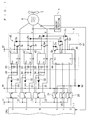
- Fig. 1 is a circuit diagram showing a configuration of a polyphase current output system to which a polyphase inverter according to the present invention is applicable.
- the system is provided with a polyphase inverter 4 and a motor 6, which is a load thereof, and is further provided with a circuit for controlling an operation of the polyphase inverter 4.
- the motor 6 drives, for example, a fan 7.
- the polyphase inverter 4 is provided with a switching circuit 45.
- the switching circuit 45 has a plurality of serial connections of high arm switching devices Qu, Qv and Qw of U-phase, V-phase and W-phase, respectively, and low arm switching devices Qx, Qy and Qz of U-phase, V-phase and W-phase, respectively.
- An IGBT insulated gate bipolar transistor
- Diodes Du, Dv, Dw, Dx, Dy and Dz are parallelly connected to each of the high arm switching devices Qu, Qv and Qw and the low arm switching devices Qx, Qy and Qz, respectively.
- a direction of a current, which these diodes apply, and a direction of the current, which the above-described switching devices apply, are opposite to each other.
- Ends of the high arm switching devices Qu, Qv and Qw on a side opposite to the low arm switching devices Qx, Qy and Qz, collectors, for example, are commonly connected.
- An electrical potential HV of about 300 V, for example, is applied to this connection point in order to be applied to the motor 6.
- a node point N1 is connected to this connection point.
- a node point N2 is connected to the node point N1 through a resistance 46.
- the node point N2 is a ground point, for example.
- connection point of the switching devices Qu and Qx for example, from the connection point of the emitter of the high arm switching device Qu and the collector of the low arm switching device Qx, an output current of U-phase is output.
- output currents of V-phase and W-phase are output, respectively. These output currents are supplied to the motor 6.
- the polyphase inverter 4 is further provided with capacitors 33, which are provided for each phase, and one ends thereof are connected to the connection points (that is to say, points at which the output current is output) of the high arm switching device and the low arm switching device for each phase.
- An electrical potential MV of 16 V for example, which is the potential higher than that of the node point N1, is supplied to the other ends of the capacitors 33 through a resistor 31 and a diode 32.
- the resistor 31 is provided in order to limit a charging current of the capacitor 33, and the diode 32 directs a forward direction thereof from a side of the above-described high electrical potential to a side of the capacitor 33 so as to prevent discharge of the capacitor 33 through the resistor 31.
- the low arm switching devices Qx, Qy and Qz are turned on, and each of the capacitors 33 corresponding to the U-phase, V-phase and W-phase are charged, respectively.
- the polyphase inverter 4 is also provided with high side control circuits 41, 42 and 43, which are provided for each phase, to control opening and closing of the high arm switching devices Qu, Qv and Qw, respectively.
- Each of the high side control circuits 41, 42 and 43 receives an operation current from the capacitor 33 of corresponding phase.
- the polyphase inverter 4 is also provided with a low side control circuit 44, which is provided for each phase, to control opening and closing of the low arm switching devices Qx, Qy and Qz.
- Components of the polyphase inverter 4 may be contained in one case, or the components other than the capacitors 33 may be contained in one case.
- Each of the high side control circuits 41, 42 and 43 has a power input ends Vcc and G, and the capacitor 33 is connected therebetween.
- the above-described one end and the other end of the capacitor 33 are connected to the power input ends G and Vcc, respectively.
- the low side control circuit 44 also has the power input ends Vcc and G, and the electrical potential MV is applied to the power input end Vcc, and the node point N2 is connected to the power input end G.
- Each of the high side control circuits 41, 42 and 43 further has an input end IN, which receives a control signal, and receive opening and closing command, which is specified by a CPU 1, as a predetermined electrical potential level.
- Switching circuits 21 to 26 and a resistor 34 are provided in order to level-shift a signal from the CPU 1 to the predetermined electrical potential level.
- the switching circuits 21 to 26 may insulate a side of the CPU 1 and a side of the high side control circuits 41, 42 and 43 and the low side control circuit 44 by using a photocoupler, for example.
- the present invention is applicable even when the photocoupler is not used and the insulation is not obtained.
- the switching circuits 21 to 23 are provided for the high side control circuits 41, 42 and 43, and an electrical potential LV (5 V, for example) corresponding to an output level of the CPU 1 is given, and both ends of the capacitor 33 are connected.
- the switching circuit 21 respectively receives a command to open and close the high arm switching device of U-phase of the CPU 1, and converts the same together with the resistor 34 to an electrical potential difference in a voltage of the both ends of the capacitor 33.
- the switching circuits 22 and 23 operate in the same way.
- the switching circuits 24 to 26 are provided for the low side control circuit 44, and the electric potential LV corresponding to the output level of the CPU 1 is given, and further, the power input ends Vcc and G of the low side control circuit 44 are connected. Therefore, the switching circuit 24 receives a command to open and close the low arm switching device of U-phase of the CPU 1 and converts the same to the electric potential difference between the electric potential MV and the node point N2.
- the switching devices 25 and 26 operate in the same way.
- Fig. 2 is a circuit diagram showing currents iu, iv and iw flowing between the switching circuit 45 and the motor 6 by setting a direction from the node point N1 toward the motor 6 to positive in a precharge period. Since all of the high arm switching devices Qu, Qv and Qw become non-conductive in the precharge period, herein, the low arm switching devices Qx, Qy and Qz, the diodes Dx, Dy and Dz parallelly connected to them, respectively, the motor 6 and the node point N1 are shown.
- the low arm switching devices Qx, Qy and Qz are in states of on, off and off, respectively, when the electrical potential of the U-phase of the motor 6 is higher than that of the V-phase and W-phase, a negative current iu flows through the low arm switching device Qx, and positive currents iu and iv flow through the diodes Dx and Dy. Also, it is required that an absolute value of the current iu ( ⁇ 0) flowing through the low arm switching device Qx is made small, as described in "Problem to be solved by the invention". Then, the low side control circuit 44 operates in a following way.
- Fig. 3 is a flow chart showing an operation of a switching for precharge of the low side control circuit 44.
- the flow chart shows an operation other than that in a case of normally driving the load.
- a procedure shifts to a flow chart of a known normal operation through "RETURN" of the flow chart.
- step S100 any one of the low arm switching devices Qx, Qy and Qz is turned on.
- step S101 it is judged whether all of the currents iu, iv and iw are not smaller than a predetermined value or not.
- the currents iu, iv and iw a direction from the connection point of the low arm switching device and the high arm switching device of each phase toward the polyphase load being set to positive, have positive values when the currents iu, iv and iw flow through the diodes Dx, Dy and Dz.
- the low arm switching devices Qx, Qy and Qz the values are negative.
- the predetermined value which is criteria of judgment, is zero or a negative value, and the absolute value thereof is selected to be smaller than the absolute value of the current, which flows without damaging the low arm switching.
- step S101 a judgment result in step S101 is affirmative (YES), and the procedure shifts to step S106.
- step S106 a normal precharge is performed. That is to say, the low arm switching devices Qx, Qy and Qz are turned on/off in a predetermined order. Thereby, when there is not a possibility that the overcurrent is generated, the normal precharge may be executed.
- step S100 may be omitted.
- step S100 is provided because the switching device to be turned on first may be easily decided.
- step S101 when the fan 7, which is driven by the motor 6, is rotated by an external cause such as a wind and the voltage is generated on the motor 6, there is a case that the judgment result in step S101 is negative (NO).
- NO negative
- any one of the currents iu, iv and iw is smaller than the negative predetermined value (if the absolute value is larger)
- the procedure shifts to step S103 and the low arm switching devices Qx, Qy and Qz are turned on, off and off, respectively.
- the procedure shifts to step S104 and the low arm switching devices Qx, Qy and Qz are turned off, on and off, respectively.
- the procedure shifts to step S105 and the low arm switching devices Qx, Qy and Qz are turned off, off and on, respectively.
- step S107 After processes of steps S103 to S106 are executed, the procedure shifts to step S107, and it is judged whether the precharge period is finished or not. If the judgment result is affirmative, the procedure shifts to the flow chart (not shown) in a case of normally driving the load, through the "RETURN".
- the low arm switching device Qz is turned on when the current iw is larger than the current iv in the above-described flow chart, and the low arm switching device Qy is turned on when the current iv is larger than the current iw.
- any one of the low arm switching devices Qy and Qz is turned on without comparing a size of the currents iv and iw, it is possible to make it difficult that the overcurrent is generated in the low arm switching device Qx, first of all.
- the low arm switching device Qz is turned on when the current iv is larger than the current iw, when the current iv is extremely large, it is highly possible that the overcurrent is easy to flow through the low arm switching device Qz. Therefore, it is preferable that the low arm switching device of the phase corresponding to the current that gives the largest value, is turned on, as in the shift from step S102 to steps S103, S104 and S105 shown in Fig. 3 . Thereby, it is possible to prevent rising of a direct current voltage based on regenerative operation status.
- the polyphase current output system shown in Fig. 1 is further provided with a current detecting circuit 5 for detecting the currents iu, iv and iw. Then the detected result is given to the CPU 1, and the control of steps S101 to S107 is performed by the CPU 1. Since a sum of the currents iu, iv and iw is zero, it is possible to omit the detection of the current iu of the U-phase as illustrated in Fig. 1 , and this may be obtained in the CPU 1 by inverting a sign of the sum of the currents iv and iw.
- Figs. 4 and 5 are graphs showing the currents iu, iv and iw, and this shows a case in which the voltage is generated by the external cause at the motor 6 in the precharge period.
- Fig. 4 shows a case of the conventional precharge
- Fig. 5 shows a case of the precharge adopting the present invention (both are simulations in which 2700 rotations/minute is supposed).
- the current iw was lower than -55 A at a point of 0.08 second (8ms), and it was recognized as the overcurrent. Thereby, the precharge is stopped (all of the switching devices were turned off), so that the currents iu, iv and iw are substantially zero.
- the absolute values of the currents iu, iv and iw are not larger than 50 A, so that the precharge continues without generating the overcurrent.
- the present invention is applicable to the polyphase load other than the motor 6.
- this is preferable when the polyphase load in which the voltage is generated by the external cause, such as the motor 6 provided with the fan 7, is adopted.
- it is preferable to apply the present invention to an air sending device provided with the polyphase inverter 4, the motor 6 and the fan 7.
- the air sending device in which the fan 7 is rotated by the external cause for example, there is an outdoor unit of an air conditioner.
Landscapes
- Engineering & Computer Science (AREA)
- Power Engineering (AREA)
- Inverter Devices (AREA)
- Control Of Ac Motors In General (AREA)
- Power Conversion In General (AREA)
- Control Of Motors That Do Not Use Commutators (AREA)
- Control Of Electric Motors In General (AREA)
Abstract
Description
- The present invention relates to a polyphase inverter adopting a bootstrap method.
- There is a polyphase inverter having a control circuit (referred to as a "high side control circuit") for driving a high arm switching device and a control circuit (referred to as a "low side control circuit") for driving a low arm switching device separately. In addition, a so-called bootstrap method in which a power source for driving the high side control circuit is obtained from a capacitor, which is charged through the low arm switching device has been proposed. Refer to, for example, the following
patent documents 1, 2 and non-patentdocument 1. -
- Patent Document 1: Japanese Patent Application Laid-Open Gazette No.
2003-348880 - Patent Document 2: Japanese Patent Application Laid-Open Gazette No.
2004-304527 - Non-Patent Document 1: Mitsubishi Electric Corporation, "Mitsubishi HVIC Application Note" [online], [searched on June 30, 2005], Internet <URL: http://www.mitsubishichips.com/Japan/files/manuals/km0020a1.pdf>
- In the bootstrap method, a period (referred to as a "precharge period") for charging the above-described capacitor for bootstrap (referred to as a "bootstrap capacitor") is set before performing a normal operation, and in this period, while the high arm switching devices are turned off, the low arm switching devices are sequentially turned on and a charge (referred to as a "precharge") of the bootstrap capacitor is performed.
-
Fig. 6 is a timing chart showing the precharge period in a three-phase inverter and on/off of the switching devices in a motor driving time following the same. For example, the low arm switching devices in U-phase, V-phase and W-phase are turned on in this order for every 500 µs in the precharge period. When a cycle in which the low arm switching devices in the three-phase are turned on is set to one cycle, the precharge period is 30 cycles, for example, that is to say, over a length of 45 ms. - When the precharge period is finished, the high arm switching devices of U-phase, V-phase and W-phase and the low arm switching devices of U-phase, V-phase and W-phase are turned on/off by a pulse width modulation control, for example, for a normal motor driving.
- However, there is a case in which a voltage is generated on a load (polyphase load) of the polyphase inverter by a cause other than the polyphase inverter. For example, in a case in which the polyphase load is the motor for driving a fan, when the fan is rotated by a wind, the voltage is generated on the motor as the polyphase load.
- Since the polyphase load is not driven from the polyphase inverter in the precharge period, such rotation of the motor is not prevented. In addition, in the precharge period, depending on timing that the low arm switching devices of U-phase, V-phase and W-phase are turned on, there is a case in which regenerating operation condition is generated and a direct voltage rises on a side of the polyphase inverter.
- In general, when such an overvoltage is generated, an overcurrent also flows through the low arm switching device. Therefore, the precharge and the normal driving of the polyphase load are not performed, in order to protect the polyphase inverter. Specifically, a current flowing through the polyphase inverter is detected and when this is excessive, a switching operation of the polyphase inverter is stopped.
- An object of the present invention is to make generation of such overcurrent difficult and to make generation of the overcurrent on the low arm switching device difficult, even when the voltage is generated on the polyphase load by an external cause in the precharge period.
- A polyphase inverter (4) according to the present invention includes a switching circuit (45), a plurality of capacitors (33), a plurality of high side control circuits (41, 42, 43) and a low side control circuit (44).
- The switching circuit has a plurality of serial connections of high arm switching devices (Qu, Qv, Qw) and low arm switching devices (Qx, Qy, Qz) provided for each phase and a plurality of diodes (Du, Dv, Dw, Dx, Dy, Dz) parallelly connected to each of the high arm switching devices and the low arm switching devices for applying a current in a direction opposite to a direction in which the high arm switching devices and the low arm switching devices apply the current. Ends of a plurality of the high arm switching devices opposite to the low arm switching devices are commonly connected, ends of a plurality of the low arm switching devices opposite to the high arm switching devices are commonly connected, and an output current is output from a connection point of the high arm switching device and the low arm switching device to a polyphase load for each phase.
- The capacitors are provided for each phase, and one end of each is connected to the connection point for each phase and is charged by conduction of the low arm switching device.
- The high side control circuits are provided for each phase, and controls opening and closing of the high arm switching devices by receiving an operation power from the corresponding capacitor.
- The low side control circuits allow the low arm switching devices provided at a phase corresponding to the output current that gives the largest value compared between phases, to conduct (S103, S104, S105), when the output current of any phase is smaller than a predetermined value, a direction from the connection point toward the polyphase load is set to positive (S102), in a period in which all of the high arm switching devices are non-conductive.
- An air sending device according to the present invention includes the polyphase inverter (4), a polyphase motor (6) being the polyphase load, and a fan (7) driven by the polyphase motor.
- A polyphase current output system according to the present invention includes the polyphase inverter or the air sending device, a current detecting circuit (5) for detecting the output current, and a control circuit (1) for controlling an operation of the low side control circuit (44) based on the output current.
- A first aspect of a control method of a polyphase inverter according to the present invention is a method for controlling a polyphase inverter (4) including a switching circuit (45), a plurality of capacitors (33), a plurality of high side control circuits (41, 42, 43), and a low side control circuit (44).
- The switching circuit has a plurality of serial connections of high arm switching devices (Qu, Qv, Qw) and low arm switching devices (Qx, Qy, Qz) provided for each phase, and a plurality of diodes (Du, Dv, Dw, Dx, Dy, Dz) parallelly connected to each of the high arm switching devices and the low arm switching devices for applying a current only in a direction opposite to a direction in which the high arm switching devices and the low arm switching devices apply the current. Ends of a plurality of the high arm switching devices opposite to the low arm switching devices are commonly connected, ends of a plurality of the low arm switching devices opposite to the high arm switching devices are commonly connected, and an output current is output from a connection point of the high arm switching device and the low arm switching device to a polyphase load for each phase.
- The capacitors are provided for each phase, one end of each is connected to the connection point for each phase, and is charged by conduction of the low arm switching device.
- The high side control circuits are provided for each phase and controls opening and closing of the high arm switching device by receiving an operation power from the corresponding capacitor. The low side control circuit controls opening and closing of the low arm switching device.
- A first aspect of the control method is such that the low arm switching device provided at a phase corresponding to the output current that gives the largest value compared between phases, is allowed to conduct (S103, S104, S105), when the output current of any phase is smaller than a predetermined value, a direction from the connection point toward the polyphase load is set to positive (S102), in a period in which all of the high arm switching devices are non-conductive.
- A second aspect of the control method of the polyphase inverter according to the present invention is the first aspect of the control method of the polyphase inverter, wherein the low arm switching devices are allowed to conduct in a predetermined order (S106), when the output current of all phases are not smaller than a predetermined value, in a period in which all of the high arm switching devices are non-conductive.
- A third aspect of the control method of the polyphase inverter according to the present invention is the first or second aspect of the control method of the polyphase inverter, wherein any one of the low arm switching devices (Qx, Qy, Qz) is exceptionally turned on only at first (S100) in a period in which all of the high arm switching devices are non-conductive.
- According to the polyphase inverter, the first aspect of the control method thereof and the polyphase current output system of the present invention, the capacitor acts as a bootstrap capacitor of the high side control circuit. Also, in a so-called precharge period in which all of the high arm switching devices are non-conductive, it becomes difficult to apply an overcurrent through the low arm switching device.
- According to the air sending device of the present invention, even when the fan receives a wind and rotates not by driving of the polyphase inverter, it is difficult that a voltage generated by the rotation applies the overcurrent through the low arm switching device.
- Also, according to the second aspect of the control method, when there is not a possibility that the overcurrent is generated, a normal precharge may be performed.
- Also, according to the third aspect of the control method, it is possible to easily decide the low arm switching device to be conducted first.
- The object, feature, aspect and advantage of the present invention will become more apparent by the following detailed description and the appended drawings.
-
-
Fig. 1 is a circuit diagram showing a configuration of a polyphase current output system to which a polyphase inverter according to the present invention is applicable. -
Fig. 2 is a circuit diagram showing currents iu, iv and iw flowing through a low switching device and a diode. -
Fig. 3 is a flow chart showing an operation of a switching for precharge of a low side control circuit according to the present invention. -
Fig. 4 is a graph showing currents iu, iv and iw in a conventional technique. -
Fig. 5 is a graph showing currents iu, iv and iw in the present invention. -
Fig. 6 is a timing chart showing a precharge period in a three-phase inverter and on/off of a switching device in a motor driving time following the same. -
Fig. 1 is a circuit diagram showing a configuration of a polyphase current output system to which a polyphase inverter according to the present invention is applicable. The system is provided with apolyphase inverter 4 and amotor 6, which is a load thereof, and is further provided with a circuit for controlling an operation of thepolyphase inverter 4. Themotor 6 drives, for example, a fan 7. - The
polyphase inverter 4 is provided with aswitching circuit 45. Theswitching circuit 45 has a plurality of serial connections of high arm switching devices Qu, Qv and Qw of U-phase, V-phase and W-phase, respectively, and low arm switching devices Qx, Qy and Qz of U-phase, V-phase and W-phase, respectively. An IGBT (insulated gate bipolar transistor), for example, may be adopted as the switching devices, in addition to a general power transistor. - Diodes Du, Dv, Dw, Dx, Dy and Dz are parallelly connected to each of the high arm switching devices Qu, Qv and Qw and the low arm switching devices Qx, Qy and Qz, respectively. A direction of a current, which these diodes apply, and a direction of the current, which the above-described switching devices apply, are opposite to each other.
- Ends of the high arm switching devices Qu, Qv and Qw on a side opposite to the low arm switching devices Qx, Qy and Qz, collectors, for example, are commonly connected. An electrical potential HV of about 300 V, for example, is applied to this connection point in order to be applied to the
motor 6. - Ends of the low arm switching devices Qx, Qy and Qz on a side opposite to the high arm switching devices Qu, Qv and Qw, emitters, for example, are commonly connected. A node point N1 is connected to this connection point. A node point N2 is connected to the node point N1 through a
resistance 46. The node point N2 is a ground point, for example. - Also, from the connection point of the switching devices Qu and Qx, for example, from the connection point of the emitter of the high arm switching device Qu and the collector of the low arm switching device Qx, an output current of U-phase is output. In the same way, from the connection points of the switching devices Qv and Qy and of the switching devices Qw and Qz, output currents of V-phase and W-phase are output, respectively. These output currents are supplied to the
motor 6. - The
polyphase inverter 4 is further provided withcapacitors 33, which are provided for each phase, and one ends thereof are connected to the connection points (that is to say, points at which the output current is output) of the high arm switching device and the low arm switching device for each phase. An electrical potential MV of 16 V, for example, which is the potential higher than that of the node point N1, is supplied to the other ends of thecapacitors 33 through aresistor 31 and adiode 32. - The
resistor 31 is provided in order to limit a charging current of thecapacitor 33, and thediode 32 directs a forward direction thereof from a side of the above-described high electrical potential to a side of thecapacitor 33 so as to prevent discharge of thecapacitor 33 through theresistor 31. - By connecting the
capacitors 33 in this way, the low arm switching devices Qx, Qy and Qz are turned on, and each of thecapacitors 33 corresponding to the U-phase, V-phase and W-phase are charged, respectively. - The
polyphase inverter 4 is also provided with highside control circuits side control circuits capacitor 33 of corresponding phase. - In addition, the
polyphase inverter 4 is also provided with a low side control circuit 44, which is provided for each phase, to control opening and closing of the low arm switching devices Qx, Qy and Qz. - Components of the
polyphase inverter 4 may be contained in one case, or the components other than thecapacitors 33 may be contained in one case. - Each of the high
side control circuits capacitor 33 is connected therebetween. The above-described one end and the other end of thecapacitor 33 are connected to the power input ends G and Vcc, respectively. - The low side control circuit 44 also has the power input ends Vcc and G, and the electrical potential MV is applied to the power input end Vcc, and the node point N2 is connected to the power input end G.
- Each of the high
side control circuits CPU 1, as a predetermined electrical potential level.Switching circuits 21 to 26 and aresistor 34 are provided in order to level-shift a signal from theCPU 1 to the predetermined electrical potential level. The switchingcircuits 21 to 26 may insulate a side of theCPU 1 and a side of the highside control circuits - The switching
circuits 21 to 23 are provided for the highside control circuits CPU 1 is given, and both ends of thecapacitor 33 are connected. - The switching
circuit 21 respectively receives a command to open and close the high arm switching device of U-phase of theCPU 1, and converts the same together with theresistor 34 to an electrical potential difference in a voltage of the both ends of thecapacitor 33. The switchingcircuits - The switching
circuits 24 to 26 are provided for the low side control circuit 44, and the electric potential LV corresponding to the output level of theCPU 1 is given, and further, the power input ends Vcc and G of the low side control circuit 44 are connected. Therefore, the switchingcircuit 24 receives a command to open and close the low arm switching device of U-phase of theCPU 1 and converts the same to the electric potential difference between the electric potential MV and the node point N2. Theswitching devices -
Fig. 2 is a circuit diagram showing currents iu, iv and iw flowing between the switchingcircuit 45 and themotor 6 by setting a direction from the node point N1 toward themotor 6 to positive in a precharge period. Since all of the high arm switching devices Qu, Qv and Qw become non-conductive in the precharge period, herein, the low arm switching devices Qx, Qy and Qz, the diodes Dx, Dy and Dz parallelly connected to them, respectively, themotor 6 and the node point N1 are shown. - In a state in which the low arm switching devices Qx, Qy and Qz are in states of on, off and off, respectively, when the electrical potential of the U-phase of the
motor 6 is higher than that of the V-phase and W-phase, a negative current iu flows through the low arm switching device Qx, and positive currents iu and iv flow through the diodes Dx and Dy. Also, it is required that an absolute value of the current iu (<0) flowing through the low arm switching device Qx is made small, as described in "Problem to be solved by the invention". Then, the low side control circuit 44 operates in a following way. -
Fig. 3 is a flow chart showing an operation of a switching for precharge of the low side control circuit 44. The flow chart shows an operation other than that in a case of normally driving the load. In a case of normally driving the load, a procedure shifts to a flow chart of a known normal operation through "RETURN" of the flow chart. - First, in step S100, any one of the low arm switching devices Qx, Qy and Qz is turned on. Next, in step S101, it is judged whether all of the currents iu, iv and iw are not smaller than a predetermined value or not. The currents iu, iv and iw, a direction from the connection point of the low arm switching device and the high arm switching device of each phase toward the polyphase load being set to positive, have positive values when the currents iu, iv and iw flow through the diodes Dx, Dy and Dz. On the other hand, when they pass through the low arm switching devices Qx, Qy and Qz, the values are negative.
- Therefore, the predetermined value, which is criteria of judgment, is zero or a negative value, and the absolute value thereof is selected to be smaller than the absolute value of the current, which flows without damaging the low arm switching.
- Then, since it is required to prevent the absolute value of the current flowing through the low arm switching device from being large, when all of the currents iu, iv and iw are not smaller than zero or a negative predetermined value, the above-described overcurrent is not problematic. In such a case, a judgment result in step S101 is affirmative (YES), and the procedure shifts to step S106.
- In step S106, a normal precharge is performed. That is to say, the low arm switching devices Qx, Qy and Qz are turned on/off in a predetermined order. Thereby, when there is not a possibility that the overcurrent is generated, the normal precharge may be executed.
- In general, all of the switching devices are turned off before the precharge, so that it is considered that all of the currents iu, iv and iw are zero, at first. Therefore, when the predetermined value is set to the negative value, the procedure shifts from step S101 to step S106. Therefore, step S100 may be omitted.
- However, it is preferable that step S100 is provided because the switching device to be turned on first may be easily decided.
- On the other hand, when the fan 7, which is driven by the
motor 6, is rotated by an external cause such as a wind and the voltage is generated on themotor 6, there is a case that the judgment result in step S101 is negative (NO). In such a case, that is to say, when any one of the currents iu, iv and iw is smaller than the negative predetermined value (if the absolute value is larger), it is judged which is the largest value. When the current iu is the largest value, the procedure shifts to step S103 and the low arm switching devices Qx, Qy and Qz are turned on, off and off, respectively. When the current iv is the largest value, the procedure shifts to step S104 and the low arm switching devices Qx, Qy and Qz are turned off, on and off, respectively. When the current iw is the largest value, the procedure shifts to step S105 and the low arm switching devices Qx, Qy and Qz are turned off, off and on, respectively. - After processes of steps S103 to S106 are executed, the procedure shifts to step S107, and it is judged whether the precharge period is finished or not. If the judgment result is affirmative, the procedure shifts to the flow chart (not shown) in a case of normally driving the load, through the "RETURN".
- If the judgment result is negative, the precharge period continues, so that the procedure returns to step S101.
- In this manner, by turning off the low arm switching device before the current, which flows through the low arm switching device of one phase, becomes the overcurrent, it becomes difficult that the overcurrent is generated. In that sense, it is possible to turn off the low arm switching device of the phase corresponding to any of the currents iu, iv and iw of which value is smaller than the predetermined value and turn on any other low arm switching device.
- For example, in an example shown in
Fig. 2 , the low arm switching device Qz is turned on when the current iw is larger than the current iv in the above-described flow chart, and the low arm switching device Qy is turned on when the current iv is larger than the current iw. However, when any one of the low arm switching devices Qy and Qz is turned on without comparing a size of the currents iv and iw, it is possible to make it difficult that the overcurrent is generated in the low arm switching device Qx, first of all. - However, if the low arm switching device Qz is turned on when the current iv is larger than the current iw, when the current iv is extremely large, it is highly possible that the overcurrent is easy to flow through the low arm switching device Qz. Therefore, it is preferable that the low arm switching device of the phase corresponding to the current that gives the largest value, is turned on, as in the shift from step S102 to steps S103, S104 and S105 shown in
Fig. 3 . Thereby, it is possible to prevent rising of a direct current voltage based on regenerative operation status. - The polyphase current output system shown in
Fig. 1 is further provided with a current detecting circuit 5 for detecting the currents iu, iv and iw. Then the detected result is given to theCPU 1, and the control of steps S101 to S107 is performed by theCPU 1. Since a sum of the currents iu, iv and iw is zero, it is possible to omit the detection of the current iu of the U-phase as illustrated inFig. 1 , and this may be obtained in theCPU 1 by inverting a sign of the sum of the currents iv and iw. -
Figs. 4 and5 are graphs showing the currents iu, iv and iw, and this shows a case in which the voltage is generated by the external cause at themotor 6 in the precharge period.Fig. 4 shows a case of the conventional precharge, andFig. 5 shows a case of the precharge adopting the present invention (both are simulations in which 2700 rotations/minute is supposed). - In
Fig. 4 , the current iw was lower than -55 A at a point of 0.08 second (8ms), and it was recognized as the overcurrent. Thereby, the precharge is stopped (all of the switching devices were turned off), so that the currents iu, iv and iw are substantially zero. - In
Fig. 5 , the absolute values of the currents iu, iv and iw are not larger than 50 A, so that the precharge continues without generating the overcurrent. - Even in a case in which the process to protect the polyphase inverter by recognizing the overcurrent in such a manner is adopted and the voltage is generated on the load by the external cause, it is possible to make the generation of the overcurrent difficult by applying the present invention and prevent suspension of the precharge.
- Of course, the present invention is applicable to the polyphase load other than the
motor 6. However, this is preferable when the polyphase load in which the voltage is generated by the external cause, such as themotor 6 provided with the fan 7, is adopted. For example, it is preferable to apply the present invention to an air sending device provided with thepolyphase inverter 4, themotor 6 and the fan 7. - As the air sending device in which the fan 7 is rotated by the external cause, for example, there is an outdoor unit of an air conditioner.
- Although the present invention has been described in detail, the above-described description is an illustration in every aspect and the present invention is not limited to this. It is considered that a number of alternative examples, which are not illustrated, may be conceived without deviating from the scope of the present invention.
Claims (6)
- A polyphase inverter (4), comprising:a switching circuit (45) having:a plurality of serial connections of high arm switching devices (Qu, Qv, Qw) and low arm switching devices (Qx, Qy, Qz) provided for each phase; anda plurality of diodes (Du, Dv, Dw, Dx, Dy, Dz) parallelly connected to each of said high arm switching devices and said low arm switching devices for applying a current only in a direction opposite to a direction in which said high arm switching devices and said low arm switching devices apply the current, ends of a plurality of said high arm switching devices opposite to said low arm switching devices being commonly connected, ends of a plurality of said low arm switching devices opposite to said high arm switching devices being commonly connected, and outputting an output current from a connection point of said high arm switching device and said low arm switching device toward a polyphase load for each phase;a plurality of capacitors (33) charged by conduction of said low arm switching devices, provided for each phase, one end of each being connected to said connection point for each phase;a plurality of high side control circuits (41, 42, 43) provided for each phase for controlling opening and closing of said high arm switching devices by receiving an operation power from corresponding said capacitor; anda low side control circuit (44) for allowing said low arm switching device provided at a phase corresponding to said output current that gives the largest value compared between phases to conduct (S103, S104, S105), when said output current of any phase is smaller than a predetermined value, a direction from said connection point to said polyphase load being set to positive (S102), in a period in which all of said high arm switching devices are non-conductive.
- An air sending device, comprising:the polyphase inverter (4) according to Claim 1;a polyphase motor (6) being said polyphase load; anda fan (7) driven by said polyphase motor.
- A polyphase current output system, comprising:the polyphase inverter according to Claim 1 or the air sending device according to Claim 2;a current detecting circuit (5) for detecting said output current; anda control circuit (1) for controlling an operation of said low side control circuit (44) based on said output current.
- A method for controlling a polyphase inverter comprising:a switching circuit (45) having:a plurality of serial connections of high arm switching devices (Qu, Qv, Qw) and low arm switching devices (Qx, Qy, Qz) provided for each phase; anda plurality of diodes (Du, Dv, Dw, Dx, Dy, Dz) parallelly connected to each of said high arm switching devices and said low arm switching devices for applying a current only in a direction opposite to a direction in which said high arm switching devices and said low arm switching devices apply the current, ends of a plurality of said high arm switching devices opposite to said low arm switching devices being commonly connected, ends of a plurality of said low arm switching devices opposite to said high arm switching devices being commonly connected, and outputting an output current from a connection point of said high arm switching device and said low arm switching device toward a polyphase load for each phase;a plurality of capacitors (33) charged by conduction of said low arm switching device, provided for each phase, one end of each being connected to said connection point for each phase;a plurality of high side control circuits (41, 42, 43) provided for each phase for controlling opening and closing of said high arm switching devices by receiving an operation power from corresponding said capacitor; anda low side control circuit (44) for controlling opening and closing of said low arm switching device,said method allowing said low arm switching device provided at a phase corresponding to said output current that gives the largest value compared between phases to conduct (S103, S104, S105), when said output current of any phase is smaller than a predetermined value, a direction from said connection point toward said polyphase load being set to positive (S102), in a period in which all of said high arm switching devices are non-conductive.
- The method for controlling the polyphase inverter according to Claim 4, wherein said low arm switching device is allowed to conduct in a predetermined order (S106) when said output current of all phases is not smaller than a predetermined value, in a period in which all of said high arm switching devices are non-conductive.
- The method for controlling the polyphase inverter according to Claim 4 or 5, wherein any one of said low arm switching devices (Qx, Qy, Qz) is exceptionally turned on only at first, in a period in which all of said high arm switching devices are non-conductive.
Applications Claiming Priority (2)
| Application Number | Priority Date | Filing Date | Title |
|---|---|---|---|
| JP2005203295A JP3876914B2 (en) | 2005-07-12 | 2005-07-12 | Multiphase inverter, control method therefor, blower, and multiphase current output system |
| PCT/JP2006/309761 WO2007007466A1 (en) | 2005-07-12 | 2006-05-16 | Polyphase inverter, control method therefor, blower, and polyphase current output system |
Publications (3)
| Publication Number | Publication Date |
|---|---|
| EP1914873A1 true EP1914873A1 (en) | 2008-04-23 |
| EP1914873A4 EP1914873A4 (en) | 2009-05-13 |
| EP1914873B1 EP1914873B1 (en) | 2010-12-01 |
Family
ID=37636866
Family Applications (1)
| Application Number | Title | Priority Date | Filing Date |
|---|---|---|---|
| EP06746475A Expired - Lifetime EP1914873B1 (en) | 2005-07-12 | 2006-05-16 | Polyphase inverter, control method therefor, blower, and polyphase current output system |
Country Status (10)
| Country | Link |
|---|---|
| US (1) | US7684217B2 (en) |
| EP (1) | EP1914873B1 (en) |
| JP (1) | JP3876914B2 (en) |
| KR (1) | KR101198566B1 (en) |
| CN (1) | CN101218742B (en) |
| AT (1) | ATE490592T1 (en) |
| AU (1) | AU2006267785B2 (en) |
| DE (1) | DE602006018623D1 (en) |
| ES (1) | ES2354717T3 (en) |
| WO (1) | WO2007007466A1 (en) |
Cited By (1)
| Publication number | Priority date | Publication date | Assignee | Title |
|---|---|---|---|---|
| WO2011100971A3 (en) * | 2010-02-18 | 2013-03-21 | Danfoss Drives A/S | Method for implementing bootstrap-supply charging in a motor controller at energized motor and motor controller using such a method |
Families Citing this family (13)
| Publication number | Priority date | Publication date | Assignee | Title |
|---|---|---|---|---|
| KR101691088B1 (en) | 2010-02-17 | 2016-12-29 | 삼성전자주식회사 | Nonvolatile memory device, operating method thereof and memory system including the same |
| KR101691092B1 (en) | 2010-08-26 | 2016-12-30 | 삼성전자주식회사 | Nonvolatile memory device, operating method thereof and memory system including the same |
| KR101658479B1 (en) * | 2010-02-09 | 2016-09-21 | 삼성전자주식회사 | Nonvolatile memory device, operating method thereof and memory system including the same |
| US9378831B2 (en) | 2010-02-09 | 2016-06-28 | Samsung Electronics Co., Ltd. | Nonvolatile memory devices, operating methods thereof and memory systems including the same |
| US8923060B2 (en) | 2010-02-17 | 2014-12-30 | Samsung Electronics Co., Ltd. | Nonvolatile memory devices and operating methods thereof |
| JP2011170956A (en) | 2010-02-18 | 2011-09-01 | Samsung Electronics Co Ltd | Nonvolatile memory device, programming method thereof and memory system including the same |
| US8792282B2 (en) | 2010-03-04 | 2014-07-29 | Samsung Electronics Co., Ltd. | Nonvolatile memory devices, memory systems and computing systems |
| EP2714339B1 (en) | 2011-06-02 | 2018-01-03 | Black & Decker Inc. | Control system for a fastening power tool |
| JP5893127B2 (en) * | 2012-03-07 | 2016-03-23 | 三菱電機株式会社 | Air conditioner |
| KR101412875B1 (en) | 2012-10-04 | 2014-07-02 | 삼성전기주식회사 | Gate driving circuit and inverter having the same |
| KR102242022B1 (en) | 2013-09-16 | 2021-04-21 | 삼성전자주식회사 | Nonvolatile memory device and program method using thereof |
| CN105305790B (en) * | 2015-11-25 | 2018-06-12 | 珠海格力电器股份有限公司 | Bootstrap circuit control method and control system |
| CN115333431B (en) * | 2022-08-31 | 2025-08-05 | 深圳拓邦股份有限公司 | Pre-charging control method, device, equipment and storage medium for fan motor |
Family Cites Families (15)
| Publication number | Priority date | Publication date | Assignee | Title |
|---|---|---|---|---|
| CA2054319C (en) * | 1991-06-28 | 1995-01-17 | Hirokazu Ioroi | Power supply unit for arc processing |
| JP3362753B2 (en) | 1995-06-20 | 2003-01-07 | 株式会社安川電機 | Inverter-driven induction motor braking method |
| JP3254968B2 (en) * | 1995-07-12 | 2002-02-12 | 松下電器産業株式会社 | Induction motor drive |
| JPH0965689A (en) * | 1995-08-28 | 1997-03-07 | Matsushita Electric Ind Co Ltd | Induction motor drive |
| DE19845903A1 (en) * | 1998-10-05 | 2000-04-06 | Aloys Wobben | Electrical power transmission system |
| JP3635988B2 (en) | 1999-05-27 | 2005-04-06 | 富士電機デバイステクノロジー株式会社 | Semiconductor device |
| JP3716702B2 (en) * | 2000-03-27 | 2005-11-16 | ダイキン工業株式会社 | How to charge the bootstrap capacitor |
| US6741482B2 (en) * | 2001-09-14 | 2004-05-25 | Kabushiki Kaisha Toshiba | Power conversion device |
| JP2003102180A (en) * | 2001-09-21 | 2003-04-04 | Hitachi Ltd | Modular inverter device for train |
| US20030076696A1 (en) * | 2001-10-18 | 2003-04-24 | Delta Electronics, Inc. | Device of uninterruptible power supply |
| JP4200351B2 (en) | 2002-05-24 | 2008-12-24 | 株式会社富士通ゼネラル | Motor control device and control method thereof |
| JP2004015892A (en) * | 2002-06-05 | 2004-01-15 | Toshiba Corp | Inverter control device and electric vehicle |
| JP4055992B2 (en) * | 2002-12-25 | 2008-03-05 | サンデン株式会社 | Inverter current detector |
| JP2004304527A (en) | 2003-03-31 | 2004-10-28 | Hitachi Ltd | Gate drive circuit and power supply control method thereof |
| US7050311B2 (en) * | 2003-11-25 | 2006-05-23 | Electric Power Research Institute, Inc. | Multilevel converter based intelligent universal transformer |
-
2005
- 2005-07-12 JP JP2005203295A patent/JP3876914B2/en not_active Expired - Fee Related
-
2006
- 2006-05-16 AU AU2006267785A patent/AU2006267785B2/en not_active Ceased
- 2006-05-16 CN CN2006800248744A patent/CN101218742B/en not_active Expired - Fee Related
- 2006-05-16 EP EP06746475A patent/EP1914873B1/en not_active Expired - Lifetime
- 2006-05-16 KR KR1020077029885A patent/KR101198566B1/en not_active Expired - Fee Related
- 2006-05-16 ES ES06746475T patent/ES2354717T3/en not_active Expired - Lifetime
- 2006-05-16 WO PCT/JP2006/309761 patent/WO2007007466A1/en not_active Ceased
- 2006-05-16 DE DE602006018623T patent/DE602006018623D1/en not_active Expired - Lifetime
- 2006-05-16 US US11/988,552 patent/US7684217B2/en not_active Expired - Fee Related
- 2006-05-16 AT AT06746475T patent/ATE490592T1/en not_active IP Right Cessation
Cited By (2)
| Publication number | Priority date | Publication date | Assignee | Title |
|---|---|---|---|---|
| WO2011100971A3 (en) * | 2010-02-18 | 2013-03-21 | Danfoss Drives A/S | Method for implementing bootstrap-supply charging in a motor controller at energized motor and motor controller using such a method |
| US8860344B2 (en) | 2010-02-18 | 2014-10-14 | Danfoss Drives A/S | Method for implementing bootstrap-supply charging in a motor controller at energized motor and motor controller using such a method |
Also Published As
| Publication number | Publication date |
|---|---|
| ES2354717T3 (en) | 2011-03-17 |
| KR20080016665A (en) | 2008-02-21 |
| JP3876914B2 (en) | 2007-02-07 |
| US7684217B2 (en) | 2010-03-23 |
| CN101218742B (en) | 2010-07-14 |
| JP2007028708A (en) | 2007-02-01 |
| KR101198566B1 (en) | 2012-11-06 |
| AU2006267785B2 (en) | 2010-01-21 |
| WO2007007466A1 (en) | 2007-01-18 |
| EP1914873B1 (en) | 2010-12-01 |
| ATE490592T1 (en) | 2010-12-15 |
| EP1914873A4 (en) | 2009-05-13 |
| CN101218742A (en) | 2008-07-09 |
| AU2006267785A1 (en) | 2007-01-18 |
| US20090027935A1 (en) | 2009-01-29 |
| DE602006018623D1 (en) | 2011-01-13 |
Similar Documents
| Publication | Publication Date | Title |
|---|---|---|
| EP1914873B1 (en) | Polyphase inverter, control method therefor, blower, and polyphase current output system | |
| US20260081539A1 (en) | Multi-level inverter | |
| JP6104660B2 (en) | Short-circuit current protection device | |
| US20160211767A1 (en) | Inverter controller and control method of inverter device | |
| EP2560283A1 (en) | Short-circuit protection method | |
| JP6426465B2 (en) | Power converter | |
| US11133795B2 (en) | Overcurrent determining apparatus and drive unit using the same | |
| CN110168922A (en) | Motor drive and electric power steering | |
| CN112534720B (en) | Drive circuit | |
| JP2023053563A (en) | Power supply device | |
| JP4655056B2 (en) | Driving device for switching element | |
| JP2022039105A (en) | Semiconductor module | |
| JP6392464B2 (en) | VEHICLE DRIVE DEVICE, VEHICLE DRIVE SYSTEM, AND CONTROL METHOD FOR VEHICLE DRIVE DEVICE | |
| JP4767781B2 (en) | Inverter device | |
| JP2001275366A (en) | Bootstrap capacitor charging method | |
| JP6231023B2 (en) | Method for controlling a power bridge and corresponding control device, power bridge and rotating electromechanical system | |
| EP3716464A1 (en) | An inverter circuit, inverter, and control method and apparatus of an inverter circuit | |
| CN108028612B (en) | Inverter device for electric vehicle | |
| JP5017529B2 (en) | Power converter for magnet synchronous motor | |
| JP2020065385A (en) | Power converter | |
| CN121312054A (en) | Multilevel inverter | |
| KR20050101725A (en) | A inverter driving device |
Legal Events
| Date | Code | Title | Description |
|---|---|---|---|
| PUAI | Public reference made under article 153(3) epc to a published international application that has entered the european phase |
Free format text: ORIGINAL CODE: 0009012 |
|
| 17P | Request for examination filed |
Effective date: 20080124 |
|
| AK | Designated contracting states |
Kind code of ref document: A1 Designated state(s): AT BE BG CH CY CZ DE DK EE ES FI FR GB GR HU IE IS IT LI LT LU LV MC NL PL PT RO SE SI SK TR |
|
| RIC1 | Information provided on ipc code assigned before grant |
Ipc: H02M 7/5387 20070101ALI20080527BHEP Ipc: H02M 7/48 20070101ALI20080527BHEP Ipc: H02P 27/06 20060101AFI20080527BHEP |
|
| A4 | Supplementary search report drawn up and despatched |
Effective date: 20090417 |
|
| GRAP | Despatch of communication of intention to grant a patent |
Free format text: ORIGINAL CODE: EPIDOSNIGR1 |
|
| GRAS | Grant fee paid |
Free format text: ORIGINAL CODE: EPIDOSNIGR3 |
|
| GRAA | (expected) grant |
Free format text: ORIGINAL CODE: 0009210 |
|
| AK | Designated contracting states |
Kind code of ref document: B1 Designated state(s): AT BE BG CH CY CZ DE DK EE ES FI FR GB GR HU IE IS IT LI LT LU LV MC NL PL PT RO SE SI SK TR |
|
| REG | Reference to a national code |
Ref country code: GB Ref legal event code: FG4D |
|
| REG | Reference to a national code |
Ref country code: CH Ref legal event code: EP |
|
| REG | Reference to a national code |
Ref country code: IE Ref legal event code: FG4D |
|
| REF | Corresponds to: |
Ref document number: 602006018623 Country of ref document: DE Date of ref document: 20110113 Kind code of ref document: P |
|
| REG | Reference to a national code |
Ref country code: ES Ref legal event code: FG2A Effective date: 20110307 |
|
| REG | Reference to a national code |
Ref country code: NL Ref legal event code: VDEP Effective date: 20101201 |
|
| PG25 | Lapsed in a contracting state [announced via postgrant information from national office to epo] |
Ref country code: LT Free format text: LAPSE BECAUSE OF FAILURE TO SUBMIT A TRANSLATION OF THE DESCRIPTION OR TO PAY THE FEE WITHIN THE PRESCRIBED TIME-LIMIT Effective date: 20101201 |
|
| LTIE | Lt: invalidation of european patent or patent extension |
Effective date: 20101201 |
|
| PG25 | Lapsed in a contracting state [announced via postgrant information from national office to epo] |
Ref country code: BG Free format text: LAPSE BECAUSE OF FAILURE TO SUBMIT A TRANSLATION OF THE DESCRIPTION OR TO PAY THE FEE WITHIN THE PRESCRIBED TIME-LIMIT Effective date: 20110301 Ref country code: FI Free format text: LAPSE BECAUSE OF FAILURE TO SUBMIT A TRANSLATION OF THE DESCRIPTION OR TO PAY THE FEE WITHIN THE PRESCRIBED TIME-LIMIT Effective date: 20101201 Ref country code: CY Free format text: LAPSE BECAUSE OF FAILURE TO SUBMIT A TRANSLATION OF THE DESCRIPTION OR TO PAY THE FEE WITHIN THE PRESCRIBED TIME-LIMIT Effective date: 20101201 Ref country code: LV Free format text: LAPSE BECAUSE OF FAILURE TO SUBMIT A TRANSLATION OF THE DESCRIPTION OR TO PAY THE FEE WITHIN THE PRESCRIBED TIME-LIMIT Effective date: 20101201 Ref country code: NL Free format text: LAPSE BECAUSE OF FAILURE TO SUBMIT A TRANSLATION OF THE DESCRIPTION OR TO PAY THE FEE WITHIN THE PRESCRIBED TIME-LIMIT Effective date: 20101201 Ref country code: AT Free format text: LAPSE BECAUSE OF FAILURE TO SUBMIT A TRANSLATION OF THE DESCRIPTION OR TO PAY THE FEE WITHIN THE PRESCRIBED TIME-LIMIT Effective date: 20101201 Ref country code: SI Free format text: LAPSE BECAUSE OF FAILURE TO SUBMIT A TRANSLATION OF THE DESCRIPTION OR TO PAY THE FEE WITHIN THE PRESCRIBED TIME-LIMIT Effective date: 20101201 Ref country code: SE Free format text: LAPSE BECAUSE OF FAILURE TO SUBMIT A TRANSLATION OF THE DESCRIPTION OR TO PAY THE FEE WITHIN THE PRESCRIBED TIME-LIMIT Effective date: 20101201 |
|
| PG25 | Lapsed in a contracting state [announced via postgrant information from national office to epo] |
Ref country code: GR Free format text: LAPSE BECAUSE OF FAILURE TO SUBMIT A TRANSLATION OF THE DESCRIPTION OR TO PAY THE FEE WITHIN THE PRESCRIBED TIME-LIMIT Effective date: 20110302 |
|
| PG25 | Lapsed in a contracting state [announced via postgrant information from national office to epo] |
Ref country code: BE Free format text: LAPSE BECAUSE OF FAILURE TO SUBMIT A TRANSLATION OF THE DESCRIPTION OR TO PAY THE FEE WITHIN THE PRESCRIBED TIME-LIMIT Effective date: 20101201 Ref country code: IS Free format text: LAPSE BECAUSE OF FAILURE TO SUBMIT A TRANSLATION OF THE DESCRIPTION OR TO PAY THE FEE WITHIN THE PRESCRIBED TIME-LIMIT Effective date: 20110401 Ref country code: PT Free format text: LAPSE BECAUSE OF FAILURE TO SUBMIT A TRANSLATION OF THE DESCRIPTION OR TO PAY THE FEE WITHIN THE PRESCRIBED TIME-LIMIT Effective date: 20110401 Ref country code: EE Free format text: LAPSE BECAUSE OF FAILURE TO SUBMIT A TRANSLATION OF THE DESCRIPTION OR TO PAY THE FEE WITHIN THE PRESCRIBED TIME-LIMIT Effective date: 20101201 Ref country code: CZ Free format text: LAPSE BECAUSE OF FAILURE TO SUBMIT A TRANSLATION OF THE DESCRIPTION OR TO PAY THE FEE WITHIN THE PRESCRIBED TIME-LIMIT Effective date: 20101201 |
|
| PG25 | Lapsed in a contracting state [announced via postgrant information from national office to epo] |
Ref country code: PL Free format text: LAPSE BECAUSE OF FAILURE TO SUBMIT A TRANSLATION OF THE DESCRIPTION OR TO PAY THE FEE WITHIN THE PRESCRIBED TIME-LIMIT Effective date: 20101201 Ref country code: SK Free format text: LAPSE BECAUSE OF FAILURE TO SUBMIT A TRANSLATION OF THE DESCRIPTION OR TO PAY THE FEE WITHIN THE PRESCRIBED TIME-LIMIT Effective date: 20101201 Ref country code: RO Free format text: LAPSE BECAUSE OF FAILURE TO SUBMIT A TRANSLATION OF THE DESCRIPTION OR TO PAY THE FEE WITHIN THE PRESCRIBED TIME-LIMIT Effective date: 20101201 |
|
| PLBE | No opposition filed within time limit |
Free format text: ORIGINAL CODE: 0009261 |
|
| STAA | Information on the status of an ep patent application or granted ep patent |
Free format text: STATUS: NO OPPOSITION FILED WITHIN TIME LIMIT |
|
| PG25 | Lapsed in a contracting state [announced via postgrant information from national office to epo] |
Ref country code: DK Free format text: LAPSE BECAUSE OF FAILURE TO SUBMIT A TRANSLATION OF THE DESCRIPTION OR TO PAY THE FEE WITHIN THE PRESCRIBED TIME-LIMIT Effective date: 20101201 |
|
| 26N | No opposition filed |
Effective date: 20110902 |
|
| REG | Reference to a national code |
Ref country code: DE Ref legal event code: R097 Ref document number: 602006018623 Country of ref document: DE Effective date: 20110902 |
|
| PG25 | Lapsed in a contracting state [announced via postgrant information from national office to epo] |
Ref country code: MC Free format text: LAPSE BECAUSE OF NON-PAYMENT OF DUE FEES Effective date: 20110531 |
|
| REG | Reference to a national code |
Ref country code: CH Ref legal event code: PL |
|
| PG25 | Lapsed in a contracting state [announced via postgrant information from national office to epo] |
Ref country code: CH Free format text: LAPSE BECAUSE OF NON-PAYMENT OF DUE FEES Effective date: 20110531 Ref country code: LI Free format text: LAPSE BECAUSE OF NON-PAYMENT OF DUE FEES Effective date: 20110531 |
|
| REG | Reference to a national code |
Ref country code: IE Ref legal event code: MM4A |
|
| PG25 | Lapsed in a contracting state [announced via postgrant information from national office to epo] |
Ref country code: IE Free format text: LAPSE BECAUSE OF NON-PAYMENT OF DUE FEES Effective date: 20110516 |
|
| PG25 | Lapsed in a contracting state [announced via postgrant information from national office to epo] |
Ref country code: LU Free format text: LAPSE BECAUSE OF NON-PAYMENT OF DUE FEES Effective date: 20110516 |
|
| PG25 | Lapsed in a contracting state [announced via postgrant information from national office to epo] |
Ref country code: TR Free format text: LAPSE BECAUSE OF FAILURE TO SUBMIT A TRANSLATION OF THE DESCRIPTION OR TO PAY THE FEE WITHIN THE PRESCRIBED TIME-LIMIT Effective date: 20101201 |
|
| PG25 | Lapsed in a contracting state [announced via postgrant information from national office to epo] |
Ref country code: HU Free format text: LAPSE BECAUSE OF FAILURE TO SUBMIT A TRANSLATION OF THE DESCRIPTION OR TO PAY THE FEE WITHIN THE PRESCRIBED TIME-LIMIT Effective date: 20101201 |
|
| PGFP | Annual fee paid to national office [announced via postgrant information from national office to epo] |
Ref country code: ES Payment date: 20140411 Year of fee payment: 9 |
|
| REG | Reference to a national code |
Ref country code: FR Ref legal event code: PLFP Year of fee payment: 11 |
|
| REG | Reference to a national code |
Ref country code: ES Ref legal event code: FD2A Effective date: 20160629 |
|
| PG25 | Lapsed in a contracting state [announced via postgrant information from national office to epo] |
Ref country code: ES Free format text: LAPSE BECAUSE OF NON-PAYMENT OF DUE FEES Effective date: 20150517 |
|
| REG | Reference to a national code |
Ref country code: FR Ref legal event code: PLFP Year of fee payment: 12 |
|
| PGFP | Annual fee paid to national office [announced via postgrant information from national office to epo] |
Ref country code: GB Payment date: 20170510 Year of fee payment: 12 Ref country code: FR Payment date: 20170413 Year of fee payment: 12 Ref country code: DE Payment date: 20170509 Year of fee payment: 12 |
|
| PGFP | Annual fee paid to national office [announced via postgrant information from national office to epo] |
Ref country code: IT Payment date: 20170522 Year of fee payment: 12 |
|
| REG | Reference to a national code |
Ref country code: DE Ref legal event code: R119 Ref document number: 602006018623 Country of ref document: DE |
|
| GBPC | Gb: european patent ceased through non-payment of renewal fee |
Effective date: 20180516 |
|
| PG25 | Lapsed in a contracting state [announced via postgrant information from national office to epo] |
Ref country code: FR Free format text: LAPSE BECAUSE OF NON-PAYMENT OF DUE FEES Effective date: 20180531 Ref country code: IT Free format text: LAPSE BECAUSE OF NON-PAYMENT OF DUE FEES Effective date: 20180516 Ref country code: DE Free format text: LAPSE BECAUSE OF NON-PAYMENT OF DUE FEES Effective date: 20181201 Ref country code: GB Free format text: LAPSE BECAUSE OF NON-PAYMENT OF DUE FEES Effective date: 20180516 |