EP1909351A1 - Reflection-type bandpass filter - Google Patents
Reflection-type bandpass filter Download PDFInfo
- Publication number
- EP1909351A1 EP1909351A1 EP07117701A EP07117701A EP1909351A1 EP 1909351 A1 EP1909351 A1 EP 1909351A1 EP 07117701 A EP07117701 A EP 07117701A EP 07117701 A EP07117701 A EP 07117701A EP 1909351 A1 EP1909351 A1 EP 1909351A1
- Authority
- EP
- European Patent Office
- Prior art keywords
- ghz
- reflection
- bandpass filter
- center conductor
- type bandpass
- Prior art date
- Legal status (The legal status is an assumption and is not a legal conclusion. Google has not performed a legal analysis and makes no representation as to the accuracy of the status listed.)
- Granted
Links
- 239000004020 conductor Substances 0.000 claims abstract description 121
- 239000000758 substrate Substances 0.000 claims abstract description 15
- 238000004891 communication Methods 0.000 claims abstract description 6
- 238000009826 distribution Methods 0.000 claims description 18
- 238000000034 method Methods 0.000 claims description 10
- 230000005540 biological transmission Effects 0.000 claims description 8
- 238000013461 design Methods 0.000 claims description 7
- 239000002184 metal Substances 0.000 claims description 6
- 229910052751 metal Inorganic materials 0.000 claims description 6
- 230000003595 spectral effect Effects 0.000 claims description 4
- 230000001902 propagating effect Effects 0.000 description 4
- RYGMFSIKBFXOCR-UHFFFAOYSA-N Copper Chemical compound [Cu] RYGMFSIKBFXOCR-UHFFFAOYSA-N 0.000 description 3
- 229910052802 copper Inorganic materials 0.000 description 3
- 239000010949 copper Substances 0.000 description 3
- 230000008878 coupling Effects 0.000 description 3
- 238000010168 coupling process Methods 0.000 description 3
- 238000005859 coupling reaction Methods 0.000 description 3
- 238000004519 manufacturing process Methods 0.000 description 3
- 238000005516 engineering process Methods 0.000 description 2
- 238000001228 spectrum Methods 0.000 description 2
- 238000006467 substitution reaction Methods 0.000 description 2
- 238000007792 addition Methods 0.000 description 1
- 230000003247 decreasing effect Effects 0.000 description 1
- 239000000463 material Substances 0.000 description 1
- 238000012986 modification Methods 0.000 description 1
- 230000004048 modification Effects 0.000 description 1
- 230000035699 permeability Effects 0.000 description 1
- 230000008569 process Effects 0.000 description 1
- 238000012545 processing Methods 0.000 description 1
- 230000002194 synthesizing effect Effects 0.000 description 1
- 230000009466 transformation Effects 0.000 description 1
- 230000007704 transition Effects 0.000 description 1
Images






Classifications
-
- H—ELECTRICITY
- H01—ELECTRIC ELEMENTS
- H01P—WAVEGUIDES; RESONATORS, LINES, OR OTHER DEVICES OF THE WAVEGUIDE TYPE
- H01P1/00—Auxiliary devices
- H01P1/20—Frequency-selective devices, e.g. filters
- H01P1/201—Filters for transverse electromagnetic waves
- H01P1/203—Strip line filters
-
- H—ELECTRICITY
- H01—ELECTRIC ELEMENTS
- H01P—WAVEGUIDES; RESONATORS, LINES, OR OTHER DEVICES OF THE WAVEGUIDE TYPE
- H01P1/00—Auxiliary devices
- H01P1/20—Frequency-selective devices, e.g. filters
- H01P1/201—Filters for transverse electromagnetic waves
- H01P1/2013—Coplanar line filters
Definitions
- This invention relates to a reflection-type bandpass filter for use in ultra-wideband (UWB) wireless data communication.
- UWB ultra-wideband
- This invention relates to a reflection-type bandpass filter for use in ultra-wideband (hereafter "UWB”) wireless data communication.
- UWB ultra-wideband
- bandpass filters proposed in the prior art may not satisfy the FCC specifications, due to manufacturing tolerances and other reasons.
- bandpass filters which use coplanar strips do not use wide ground strips, and so are not suitable for coupling with transmission lines such as slot lines.
- This invention was devised in light of the above circumstances, and has as an object the provision of a high-performance UWB reflection-type bandpass filter which has excellent coupling characteristics with transmission lines such as slot lines, and which satisfies FCC specifications.
- This invention provides a reflection-type bandpass filter for ultra-wideband wireless data communication, in which are provided on the surface of a dielectric substrate a center conductor and side conductors provided on both sides of the center conductor securing a prescribed distance between conductors with non-conducting portions intervening, and in which the center conductor width or the distances between conductors, or both, are distributed non-uniformly in a length direction of the center conductor.
- the center conductor width may be constant, and the distances between conductors may be distributed non-uniformly.
- the distances between conductors may be constant, and the center conductor width may be distributed non-uniformly.
- a difference of 10 dB or higher may exist between a reflectance in a ranges of frequencies f for which f ⁇ 3.1 GHz and f > 10.6 GHz, and a reflectance in a range of frequencies 3.9 GHz ⁇ f ⁇ 9.8 GHz, and in a range 3.9 GHz ⁇ f ⁇ 9.8 GHz a group delay variation may be within ⁇ 0.1 ns.
- a difference of 10 dB or higher may exist between a reflectance in a range of frequencies f for which f ⁇ 3.1 GHz and f > 10.6 GHz, and a reflectance in a range of frequencies 3.7 GHz ⁇ f ⁇ 10.0 GHz, and in a range 3.7 GHz ⁇ f ⁇ 10.0 GHz a group delay variation may be within ⁇ 0.1 ns.
- a difference of 10 dB or higher may exist between a reflectance in a range of frequencies f for which f ⁇ 3.1 GHz and f > 10.6 GHz, and a reflectance in a range of frequencies 4.1 GHz ⁇ f ⁇ 9.5 GHz, and in a range 4.1 GHz ⁇ f ⁇ 9.5 GHz a group delay variation may be within ⁇ 0.1 ns.
- a characteristic impedance Zc of an input terminal transmission line may be in the range 10 ⁇ ⁇ Zc ⁇ 300 ⁇ .
- a resistance having the same impedance as the above characteristic impedance value, or a non-reflecting terminator, may be provided on the terminating side.
- the dielectric substrate may have a thickness h in a range 0.1 mm ⁇ h ⁇ 10 mm, a relative permittivity ⁇ r in a range 1 ⁇ ⁇ r ⁇ 500, a width W in a range 2 mm ⁇ W ⁇ 100 mm, and a length L in a range 2 mm ⁇ L ⁇ 500 mm.
- length-direction distributions of the center conductor width and of the distances between conductors may satisfy a design method based on the inverse problem of deriving a potential from spectral data in the Zakharov-Shabat equation.
- length-direction distributions of the center conductor width and of the distances between conductors may satisfy a window function method.
- length-direction distributions of the center conductor width and of the distances between conductors may satisfy a Kaiser window function method.
- a reflection-type bandpass filter of this invention by applying a window function technique to design a reflection-type bandpass filter comprising non-uniform coplanar strips, the pass band can be made extremely broad and variation in group delay within the pass band can be made extremely small compared with filters of the related art, even when manufacturing tolerances are large. As a result, a UWB bandpass filter can be provided which satisfies FCC specifications.
- ground strips can be made wide, so that easy coupling with transmission lines such as slot lines is achieved.
- ground strips refers to the conductors on both sides, which are connected together on the input end.
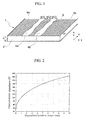
- Fig. 1 is a perspective view showing, in summary, the configuration of a reflection-type bandpass filter of an exemplary aspect of this invention.
- the symbol 1 is the reflection-type bandpass filter
- 2 is a dielectric substrate
- 3 is a center conductor
- 4a and 4b are non-conducting portions
- 5a and 5b are side conductors.
- the center conductor 3 and side conductors 5a, 5b provided on either side of the center conductor 3, maintaining a prescribed distance between conductors and with non-conducting portions 4a, 4b intervening, are formed on the surface of the dielectric substrate 2; the non-uniform coplanar strips are such that the center conductor width or the distances between conductors, or both, are distributed non-uniformly in the length direction of the center conductor 3.
- the z axis is taken along the length direction of the center conductor 3
- the y axis is taken in the direction perpendicular to the z axis and parallel to the surface of the substrate 2
- the x axis is taken in the direction perpendicular to the y axis and to the z axis.
- the length extending in the z axis direction from the end face on the input end is z.
- the conductor-to-conductor distance between the side conductor 5a and the center conductor 3, and the conductor-to-conductor distance between the side conductor 5b and the center conductor 3, are the same at each place where z is equal (hereafter the "distance between conductors s").
- the side conductors 5a and 5b are semi-infinite: in other words, the widths of the side conductors 5a and 5b are ten times or greater than the width of the center conductor 3 and the non-conducting portions 4a, 4b.
- the side conductors 5a, 5b can be used in configuring a slot line, slot antenna, or the like.
- the characteristic impedance of this reflection-type bandpass filter is low, so that the substrate 2 can be fabricated from material with a low permittivity.
- a reflection-type bandpass filter of this aspect of the invention adopts a configuration in which stop band rejection (the difference between the reflectance in the pass band, and the reflectance in the stop band) is increased, by using a window function method (see Reference 10) employed in digital filter design.
- stop band rejection the difference between the reflectance in the pass band, and the reflectance in the stop band
- a window function method see Reference 10
- the stop band rejection can be increased.
- manufacturing tolerances can be increased.
- variation in the group delay within the pass band is decreased.
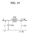
- the transmission line of a reflection-type bandpass filter 1 of this aspect of the invention can be represented by a non-uniformly distributed constant circuit such as in Fig. 19.
- Z(z) ⁇ L(z)/C(z) ⁇ is the local characteristic impedance
- ⁇ 1 , ⁇ 2 are the power wave amplitudes propagating in the +z and -z directions respectively.
- c(z) 1/ ⁇ L(z)/C(z) ⁇ . If the time factor is set to exp(j ⁇ t), and a variable transformation is performed as in equation (4) below, then the Zakharov-Shabat equation of equation (5) is obtained.
- the Zakharov-Shabat inverse problem involves synthesizing the potential q(x) from spectral data which is a solution satisfying the above equations (see Reference 11). If the potential q(x) is found, the local characteristic impedance Z(x) is determined as in equation (7) below.
- Z x Z 0 exp 2 ⁇ ⁇ 0 x q s d s .
- the reflectance coefficient r(x) in x space is calculated from the spectra data reflectance coefficient R( ⁇ ) using the following equation (8), and q(x) are obtained from r(x).
- r x 1 2 ⁇ ⁇ ⁇ - ⁇ ⁇ R ⁇ ⁇ e - j ⁇ ⁇ ⁇ x d ⁇
- a window function is applied as in equation (9) to determine r'(x) .
- r ⁇ x ⁇ x ⁇ r x .
- ⁇ (x) is the window function. If the window function is selected appropriately, the stop band rejection level can be appropriately controlled.
- a Kaiser window is used as an example. The Kaiser window is defined as in equation (10) below (see Reference 10).
- ⁇ n ⁇ I 0 ⁇ ⁇ ⁇ 1 - n - ⁇ / ⁇ 2 1 ⁇ 2 I 0 ⁇ , 0 ⁇ n ⁇ M , 0 , otherwise
- ⁇ M/s, and ⁇ is determined empirically as in equation (11) below.
- ⁇ ⁇ 0.1102 ( A - 8.7 ) , A > 50 , 0.5842 ⁇ A - 21 0.4 + 0.07886 ( A - 21 ) , 21 ⁇ A ⁇ 50 , 0 , a ⁇ 21
- the characteristic impedance can be changed (see Reference 12).
- the center conductor width w or distance between conductors s was calculated based on the local characteristic impedance obtained from equation (7), and a bandpass filter 1 was manufactured so as to satisfy the calculated center conductor width w or distance between conductors s.
- reflection-type bandpass filters 1 having the desired pass band were obtained.
- the characteristic impedance is set so as to match the impedance of the system being used.
- a system impedance of 50 ⁇ , 75 ⁇ , 300 ⁇ , or similar is used. It is desirable that the characteristic impedance Zc be in the range 10 ⁇ ⁇ Zc ⁇ 300 ⁇ . If the characteristic impedance is smaller than 10 ⁇ , then losses due to the conductor and dielectric become comparatively large. If the characteristic impedance is higher than 300 ⁇ , matching with the system impedance is not possible.
- Fig. 4 shows the distribution in the z-axis direction of the local characteristic impedance obtained in the inverse problem.
- Tables 1 through 3 list the distances between conductors s. Table 1.
- Fig. 6 shows the shape of the coplanar strip in the reflection-type bandpass filter 1 of Embodiment 1.
- the lightly shaded portion represents the center conductor 3 and the side conductors 5a and 5b, and the heavily shaded lines represent the non-conducting portions 4a and 4b.
- the non-reflecting terminator or resistance may be connected directly to the terminating end of the reflection-type bandpass filter 1.
- ⁇ , ⁇ 0 , and ⁇ are respectively the angular frequency, magnetic permeability in vacuum, and the conductivity of the metal.
- the thickness of the center conductor 3 and of the side conductors 5a, 5b may be 2.1 ⁇ m or greater.
- This bandpass filter 1 is used in a system with a characteristic impedance of 75 ⁇ .
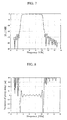
- Fig. 7 and Fig. 8 show the amplitude characteristic and group delay characteristic respectively of reflected waves (S 11 ) in the bandpass filter 1 of Embodiment 1.
- the reflectance in the range of frequencies f for which 3.9 GHz ⁇ f ⁇ 9.8 GHz, the reflectance is -2 dB or greater, and the group delay variation is within ⁇ 0.1 ns.
- the reflectance In the region f ⁇ 3.1 GHz or f > 10.6 GHz, the reflectance is -15 dB or lower.
- Fig. 9 shows the distribution in the z-axis direction of the local characteristic impedance obtained in the inverse problem.
- Tables 4 through 6 list the center conductor widths w. Table 4.
- Fig. 11 shows the shape of the coplanar strip in the reflection-type bandpass filter 1 of Embodiment 2.
- the lightly shaded portion represents the center conductor 3 and the side conductors 5a and 5b, and the heavily shaded lines represent the non-conducting portions 4a and 4b.
- the thickness of the center conductor 3 and of the side conductors 5a, 5b may be 2.1 ⁇ m or greater.
- This bandpass filter 1 is used in a system with a characteristic impedance of 75 ⁇ .
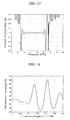
- Fig. 12 and Fig. 13 show the amplitude characteristic and group delay characteristic respectively of reflected waves (S 11 ) in the bandpass filter 1 of Embodiment 2.
- the reflectance in the range of frequencies f for which 3.7 GHz ⁇ f ⁇ 10.0 GHz, the reflectance is -5 dB or greater, and the group delay variation is within ⁇ 0.1 ns.
- the reflectance In the region f ⁇ 3.1 GHz or f > 10.6 GHz, the reflectance is -20 dB or lower.
- Fig. 14 shows the distribution in the z-axis direction of the local characteristic impedance obtained in the inverse problem.
- Table 7 lists the distances between conductors s. Table 7.
- Fig. 16 shows the shape of the coplanar strip in the reflection-type bandpass filter 1 of Embodiment 3.
- the lightly shaded portion represents the center conductor 3 and the side conductors 5a and 5b, and the heavily shaded portion represents the non-conducting portions 4a and 4b.
- the thickness of the center conductor 3 and of the side conductors 5a, 5b may be 2.1 ⁇ m or greater.
- This bandpass filter 1 is used in a system with a characteristic impedance of 50 ⁇ .
- Fig. 17 and Fig. 18 show the amplitude characteristic and group delay characteristic respectively of reflected waves (S 11 ) in the bandpass filter 1 of Embodiment 3.
- the reflectance in the range of frequencies f for which 4.1 GHz ⁇ f ⁇ 9.5 GHz, the reflectance is -5 dB or greater, and the group delay variation is within ⁇ 0.1 ns.
- the reflectance In the region f ⁇ 3.1 GHz or f > 10.6 GHz, the reflectance is -15 dB or lower.
Landscapes
- Physics & Mathematics (AREA)
- Electromagnetism (AREA)
- Control Of Motors That Do Not Use Commutators (AREA)
Abstract
Description
- This application claims priority from
Japanese Patent Application No. 2006-274323, filed on October 5, 2006 - This invention relates to a reflection-type bandpass filter for use in ultra-wideband (UWB) wireless data communication.
- This invention relates to a reflection-type bandpass filter for use in ultra-wideband (hereafter "UWB") wireless data communication. By using this UWB reflection-type bandpass filter, U.S. Federal Communications Commission requirements for spectrum masks can be satisfied.
- As technology of the prior art related to this invention, for example, the technology disclosed in the following
references 1 through 10 is known. - Reference 1: Specification of
U.S. Patent No. 2411555 - Reference 2:
Japanese Unexamined Patent Application No. 56-64501 - Reference 3:
Japanese Unexamined Patent Application No. 9-172318 - Reference 4:
Japanese Unexamined Patent Application No. 9-232820 - Reference 5:
Japanese Unexamined Patent Application No. 10-65402 - Reference 6:
Japanese Unexamined Patent Application No. 10-242746 - Reference 7:
Japanese Unexamined Patent Application No. 2000-4108 - Reference 8:
Japanese Unexamined Patent Application No. 2000-101301 - Reference 9:
Japanese Unexamined Patent Application No. 2002-43810 - Reference 10: A.V. Oppenheim and R.W. Schafer, "Discrete-time signal processing," pp. 465-478, Prentice Hall, 1998.
- Reference 11: G-B. Xiao, K. Yashiro, N. Guan, and S. Ohokawa, "An effective method for designing nonuniformly coupled transmission-line filters," IEEE Trans. Microwave Theory Tech., vol. 49, pp. 1027-1031, June 2001.
- Reference 12: Y. Konishi, "Microwave integrated circuits", pp. 19-21, Marcel Dekker, 1991
- However, the bandpass filters proposed in the prior art may not satisfy the FCC specifications, due to manufacturing tolerances and other reasons.
- Further, bandpass filters which use coplanar strips do not use wide ground strips, and so are not suitable for coupling with transmission lines such as slot lines. This invention was devised in light of the above circumstances, and has as an object the provision of a high-performance UWB reflection-type bandpass filter which has excellent coupling characteristics with transmission lines such as slot lines, and which satisfies FCC specifications.
- This invention provides a reflection-type bandpass filter for ultra-wideband wireless data communication, in which are provided on the surface of a dielectric substrate a center conductor and side conductors provided on both sides of the center conductor securing a prescribed distance between conductors with non-conducting portions intervening, and in which the center conductor width or the distances between conductors, or both, are distributed non-uniformly in a length direction of the center conductor.
- In a reflection-type bandpass filter of this invention, the center conductor width may be constant, and the distances between conductors may be distributed non-uniformly.
- Alternately, the distances between conductors may be constant, and the center conductor width may be distributed non-uniformly.
- In a reflection-type bandpass filter of this invention, a difference of 10 dB or higher may exist between a reflectance in a ranges of frequencies f for which f < 3.1 GHz and f > 10.6 GHz, and a reflectance in a range of frequencies 3.9 GHz ≤ f ≤ 9.8 GHz, and in a range 3.9 GHz ≤ f ≤ 9.8 GHz a group delay variation may be within ±0.1 ns.
- In a reflection-type bandpass filter of this invention, alternately, a difference of 10 dB or higher may exist between a reflectance in a range of frequencies f for which f < 3.1 GHz and f > 10.6 GHz, and a reflectance in a range of frequencies 3.7 GHz ≤ f ≤ 10.0 GHz, and in a range 3.7 GHz ≤ f ≤ 10.0 GHz a group delay variation may be within ±0.1 ns.
- In a reflection-type bandpass filter of this invention, alternately, a difference of 10 dB or higher may exist between a reflectance in a range of frequencies f for which f < 3.1 GHz and f > 10.6 GHz, and a reflectance in a range of frequencies 4.1 GHz ≤ f ≤ 9.5 GHz, and in a range 4.1 GHz ≤ f ≤ 9.5 GHz a group delay variation may be within ±0.1 ns.
- In a reflection-type bandpass filter of this invention, a characteristic impedance Zc of an input terminal transmission line may be in the
range 10 Ω ≤ Zc ≤ 300 Ω. - In a reflection-type bandpass filter of this invention, a resistance having the same impedance as the above characteristic impedance value, or a non-reflecting terminator, may be provided on the terminating side.
- In a reflection-type bandpass filter of this invention, the center conductor and the side conductors may comprise metal plates of thickness equal to or greater than a skin depth at f = 1 GHz.
- In a reflection-type bandpass filter of this invention, the dielectric substrate may have a thickness h in a range 0.1 mm ≤ h ≤ 10 mm, a relative permittivity εr in a
range 1 ≤ εr ≤ 500, a width W in arange 2 mm ≤ W ≤ 100 mm, and a length L in arange 2 mm ≤ L ≤ 500 mm. - In a reflection-type bandpass filter of this invention, length-direction distributions of the center conductor width and of the distances between conductors may satisfy a design method based on the inverse problem of deriving a potential from spectral data in the Zakharov-Shabat equation.
- In a reflection-type bandpass filter of this invention, length-direction distributions of the center conductor width and of the distances between conductors may satisfy a window function method.
- In a reflection-type bandpass filter of this invention, length-direction distributions of the center conductor width and of the distances between conductors may satisfy a Kaiser window function method.
- In a reflection-type bandpass filter of this invention, by applying a window function technique to design a reflection-type bandpass filter comprising non-uniform coplanar strips, the pass band can be made extremely broad and variation in group delay within the pass band can be made extremely small compared with filters of the related art, even when manufacturing tolerances are large. As a result, a UWB bandpass filter can be provided which satisfies FCC specifications.
- Further, ground strips can be made wide, so that easy coupling with transmission lines such as slot lines is achieved. Here, "ground strips" refers to the conductors on both sides, which are connected together on the input end.
-
- Fig. 1 is a perspective view showing one aspect of a reflection-type bandpass filter of the invention;
- Fig. 2 is a graph showing the conductor-to-conductor distance dependence of the characteristic impedance in the coplanar strips;
- Fig. 3 is a graph showing the center conductor width dependence of the characteristic impedance in the coplanar strips;
- Fig. 4 is a graph showing the characteristic impedance distribution of the reflection-type bandpass filter fabricated in
Embodiment 1; - Fig. 5 is a graph showing the distribution of the distance between conductors of the coplanar strip in the reflection-type bandpass filter fabricated in
Embodiment 1; - Fig. 6 is a graph showing the shape of the coplanar strip in the reflection-type bandpass filter fabricated in
Embodiment 1; - Fig. 7 is a graph showing the reflected wave amplitude characteristic in the reflection-type bandpass filter fabricated in
Embodiment 1; - Fig. 8 is a graph showing the reflected wave group delay characteristic in the reflection-type bandpass filter fabricated in
Embodiment 1; - Fig. 9 is a graph showing the characteristic impedance distribution of the reflection-type bandpass filter fabricated in
Embodiment 2; - Fig. 10 is a graph showing the distribution of the center conductor width of the coplanar strip in the reflection-type bandpass filter fabricated in
Embodiment 2; - Fig. 11 is a graph showing the shape of the coplanar strip in the reflection-type bandpass filter fabricated in
Embodiment 2; - Fig. 12 is a graph showing the reflected wave amplitude characteristic in the reflection-type bandpass filter fabricated in
Embodiment 2; - Fig. 13 is a graph showing the reflected wave group delay characteristic in the reflection-type bandpass filter fabricated in
Embodiment 2; - Fig. 14 is a graph showing the characteristic impedance distribution of the reflection-type bandpass filter fabricated in
Embodiment 3; - Fig. 15 is a graph showing the distribution of the distance between conductors of the coplanar strip in the reflection-type bandpass filter fabricated in
Embodiment 3; - Fig. 16 is a graph showing the shape of the coplanar strip in the reflection-type bandpass filter fabricated in
Embodiment 3; - Fig. 17 is a graph showing the reflected wave amplitude characteristic in the reflection-type bandpass filter fabricated in
Embodiment 3; - Fig. 18 is a graph showing the reflected wave group delay characteristic in the reflection-type bandpass filter fabricated in
Embodiment 3; and, - Fig. 19 is an equivalent circuit of a non-uniform transmission line.
- Below, exemplary aspects of the invention are explained referring to the drawings.
- Fig. 1 is a perspective view showing, in summary, the configuration of a reflection-type bandpass filter of an exemplary aspect of this invention. In the figure, the
symbol 1 is the reflection-type bandpass filter, 2 is a dielectric substrate, 3 is a center conductor, 4a and 4b are non-conducting portions, and 5a and 5b are side conductors. - In the reflection-
type bandpass filter 1 of this aspect, thecenter conductor 3 andside conductors center conductor 3, maintaining a prescribed distance between conductors and withnon-conducting portions dielectric substrate 2; the non-uniform coplanar strips are such that the center conductor width or the distances between conductors, or both, are distributed non-uniformly in the length direction of thecenter conductor 3. - As shown in Fig. 1, the z axis is taken along the length direction of the
center conductor 3, the y axis is taken in the direction perpendicular to the z axis and parallel to the surface of thesubstrate 2, and the x axis is taken in the direction perpendicular to the y axis and to the z axis. The length extending in the z axis direction from the end face on the input end is z. In the reflection-type bandpass filter 1, the conductor-to-conductor distance between theside conductor 5a and thecenter conductor 3, and the conductor-to-conductor distance between theside conductor 5b and thecenter conductor 3, are the same at each place where z is equal (hereafter the "distance between conductors s"). In this reflection-type bandpass filter, theside conductors side conductors center conductor 3 and thenon-conducting portions side conductors substrate 2 can be fabricated from material with a low permittivity. - A reflection-type bandpass filter of this aspect of the invention adopts a configuration in which stop band rejection (the difference between the reflectance in the pass band, and the reflectance in the stop band) is increased, by using a window function method (see Reference 10) employed in digital filter design. By this means, instead of expansion of the transition frequency region (the region between the pass band boundary and the stop band boundary), the stop band rejection can be increased. As a result, manufacturing tolerances can be increased. Also, variation in the group delay within the pass band is decreased.
- The transmission line of a reflection-
type bandpass filter 1 of this aspect of the invention can be represented by a non-uniformly distributed constant circuit such as in Fig. 19. - From Fig. 19, the following equation (1) is obtained for the line voltage v(z,t) and the line current i(z,t).

- Here L(z) and C(z) are the inductance and capacitance respectively per unit length in the transmission line. Here, the function of equation (2) is introduced.

- Here Z(z) = √{L(z)/C(z)} is the local characteristic impedance, and φ1, φ2 are the power wave amplitudes propagating in the +z and -z directions respectively.
- Substitution into equation (1) yields equation (3).

- Here c(z) = 1/√{L(z)/C(z)}. If the time factor is set to exp(jωt), and a variable transformation is performed as in equation (4) below, then the Zakharov-Shabat equation of equation (5) is obtained.


- Here q(x) is as given by equation (6) below.
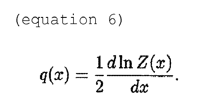
- The Zakharov-Shabat inverse problem involves synthesizing the potential q(x) from spectral data which is a solution satisfying the above equations (see Reference 11). If the potential q(x) is found, the local characteristic impedance Z(x) is determined as in equation (7) below.

- Here, normally in a process to determine the potential q(x), the reflectance coefficient r(x) in x space is calculated from the spectra data reflectance coefficient R(ω) using the following equation (8), and q(x) are obtained from r(x).

- In this invention, in place of obtaining r(x) from the R(ω) for ideal spectral data, a window function is applied as in equation (9) to determine r'(x) .

- Here ω(x) is the window function. If the window function is selected appropriately, the stop band rejection level can be appropriately controlled. Here, a Kaiser window is used as an example. The Kaiser window is defined as in equation (10) below (see Reference 10).

- Here α = M/s, and β is determined empirically as in equation (11) below.

- Here A = -20log10δ. where δ is the peak approximation error in the pass band and in the stop band.
- In this way q(x) is determined, and from equation (7) the local characteristic impedance Z(x) is determined.
- Here, when either the width w of the center conductor 6 (hereafter the "center conductor width w") or the distance between conductors s, or both, of the coplanar strips are varied, the characteristic impedance can be changed (see Reference 12).
- Fig. 2 shows the dependence of the characteristic impedance on the distance between conductors s, when the center conductor width w = 1 mm, the thickness of the
substrate 2 is 1 mm, and the relative permittivity εr of thesubstrate 2 is 4. Fig. 3 shows the dependence of the characteristic impedance on the center conductor width w, when the distance between conductors s = 1 mm, h = 1 mm, and εr = 4. - In this invention, the center conductor width w or distance between conductors s was calculated based on the local characteristic impedance obtained from equation (7), and a
bandpass filter 1 was manufactured so as to satisfy the calculated center conductor width w or distance between conductors s. By this means, reflection-type bandpass filters 1 having the desired pass band were obtained. - Below, the invention is explained in further detail referring to embodiments. Each of the embodiments described below is merely an illustration of the invention, and the invention is in no way limited to these embodiment descriptions.
- A Kaiser window was used for which the reflectance is 0.9 at frequencies f in the range 3.4 GHz ≤ f ≤ 10.3 GHz, and is 0 elsewhere, and for which A = 30. Design was performed using one wavelength of signals at a frequency f = 1 GHz propagating in the coplanar strip as the waveguide length, and setting the system characteristic impedance to 75 Ω. Here, the characteristic impedance is set so as to match the impedance of the system being used. In general, in a circuit which handles high-frequency signals, a system impedance of 50 Ω, 75 Ω, 300 Ω, or similar is used. It is desirable that the characteristic impedance Zc be in the
range 10 Ω ≤ Zc ≤ 300 Ω. If the characteristic impedance is smaller than 10 Ω, then losses due to the conductor and dielectric become comparatively large. If the characteristic impedance is higher than 300 Ω, matching with the system impedance is not possible. - Fig. 4 shows the distribution in the z-axis direction of the local characteristic impedance obtained in the inverse problem. The horizontal axis is z divided by one wavelength at f=1 GHz; similar axes are used in Fig. 9 and Fig. 14 below.
- Fig. 5 shows the distribution in the z-axis direction of the distance between conductors s, when using a
substrate 2 with a thickness h = 1 mm and relative permittivity εr = 4, and when the center conductor width w = 2 mm. Tables 1 through 3 list the distances between conductors s.Table 1. Distances between conductors (1/3) z[mm] 0.00 0.21 0.41 0.62 0.83 1.04 1.24 1.45 1.66 1.87 2.07 2.28 s[mm] 0.69 0.69 0.69 0.69 0.69 0.69 0.69 0.69 0.69 0.69 0.69 0.69 #2 2.49 2.70 2.90 3.11 3.32 3.53 3.73 3.94 4.15 4.36 4.56 4.77 - 0.69 0.69 0.69 0.69 0.69 0.70 0.70 0.70 0.70 0.70 0.70 0.71 #3 4.98 5.19 5.39 5.60 5.81 6.02 6.23 6.43 6.64 6.85 7.06 7.26 - 0.71 0.71 0.71 0.72 0.72 0.72 0.72 0.72 0.73 0.73 0.73 0.73 #4 7.47 7.68 7.89 8.10 8.31 8.51 8.72 8.93 9.14 9.35 9.55 9.76 - 0.73 0.74 0.74 0.74 0.74 0.74 0.74 0.74 0.74 0.74 0.74 0.74 #5 9.97 10.18 10.39 10.59 10.80 11.01 11.22 11.43 11.63 11.84 12.05 12.26 - 0.74 0.74 0.74 0.74 0.74 0.73 0.73 0.73 0.73 0.73 0.73 0.73 #6 12.47 12.67 12.88 13.09 13.30 13.51 13.71 13.92 14.13 14.34 14.55 14.75 - 0.73 0.73 0.73 0.73 0.73 0.73 0.73 0.73 0.73 0.73 0.73 0.73 #7 14.96 15.17 15.38 15.58 15.79 16.00 16.21 16.42 16.62 16.83 17.04 17.25 - 0.73 0.73 0.73 0.73 0.73 0.73 0.73 0.73 0.73 0.73 0.73 0.73 #8 17.46 17.66 17.87 18.08 18.29 18.50 18.70 18.91 19.12 19.33 19.54 19.74 - 0.73 0.73 0.73 0.73 0.73 0.72 0.72 0.72 0.72 0.71 0.71 0.71 #9 19.95 20.16 20.37 20.57 20.78 20.99 21.19 21.40 21.61 21.82 22.02 22.23 - 0.70 0.70 0.70 0.69 0.69 0.69 0.68 0.68 0.68 0.67 0.67 0.67 #10 22.44 22.64 22.85 23.06 23.27 23.47 23.68 23.89 24.09 24.30 24.51 24.71 - 0.67 0.66 0.66 0.66 0.66 0.66 0.66 0.66 0.66 0.66 0.66 0.66 #11 24.92 25.13 25.33 25.54 25.75 25.96 26.16 26.37 26.58 26.78 26.99 27.20 - 0.66 0.66 0.66 0.66 0.66 0.66 0.66 0.67 0.67 0.67 0.67 0.67 #12 27.41 27.61 27.82 28.03 28.23 28.44 28.65 28.86 29.06 29.27 29.48 29.68 - 0.67 0.67 0.67 0.67 0.67 0.67 0.67 0.67 0.67 0.67 0.67 0.67 #13 29.89 30.10 30.31 30.51 30.72 30.93 31.13 31.34 31.55 31.75 31.96 32.17 - 0.67 0.67 0.67 0.67 0.67 0.67 0.67 0.67 0.67 0.66 0.67 0.67 #14 32.38 32.58 32.79 33.00 33.20 33.41 33.62 33.83 34.03 34.24 34.45 34.65 - 0.67 0.67 0.67 0.67 0.67 0.67 0.68 0.68 0.68 0.69 0.69 0.69 #15 34.86 35.07 35.28 35.49 35.69 35.90 36.11 36.32 36.53 36.73 36.94 37.15 - 0.70 0.70 0.71 0.71 0.72 0.72 0.73 0.74 0.74 0.75 0.75 0.76 #16 37.36 37.57 37.78 37.98 38.19 38.40 38.61 38.82 39.03 39.24 39.44 39.65 - 0.76 0.76 0.77 0.77 0.77 0.78 0.78 0.78 0.78 0.78 0.78 0.78 #17 39.86 40.07 40.28 40.49 40.70 40.90 41.11 41.32 41.53 41.74 41.95 42.16 - 0.78 0.78 0.78 0.78 0.77 0.77 0.77 0.77 0.77 0.76 0.76 0.76 #18 42.36 42.57 42.78 42.99 43.20 43.41 43.61 43.82 44.03 44.24 44.45 44.66 - 0.76 0.76 0.76 0.75 0.75 0.75 0.75 0.75 0.75 0.75 0.76 0.76 #19 44.86 45.07 45.28 45.49 45.70 45.91 46.11 46.32 46.53 46.74 46.95 47.16 - 0.76 0.76 0.76 0.76 0.76 0.77 0.77 0.77 0.77 0.77 0.77 0.77 #20 47.37 47.57 47.78 47.99 48.20 48.41 48.62 48.82 49.03 49.24 49.45 49.66 - 0.77 0.77 0.77 0.76 0.76 0.76 0.76 0.75 0.75 0.74 0.73 0.73 #21 49.86 50.07 50.28 50.49 50.70 50.90 51.11 51.32 51.52 51.73 51.94 52.14 - 0.72 0.71 0.71 0.70 0.69 0.68 0.68 0.67 0.66 0.66 0.65 0.64 #22 52.35 52.56 52.76 52.97 53.18 53.38 53.59 53.79 54.00 54.21 54.41 54.62 - 0.64 0.63 0.63 0.62 0.62 0.61 0.61 0.61 0.61 0.60 0.60 0.60 #23 54.83 55.03 55.24 55.44 55.65 55.86 56.06 56.27 56.48 56.68 56.89 57.09 - 0.60 0.61 0.61 0.61 0.61 0.61 0.61 0.62 0.62 0.62 0.62 0.63 #24 57.30 57.51 57.71 57.92 58.13 58.33 58.54 58.75 58.95 59.16 59.37 59.57 - 0.63 0.63 0.63 0.63 0.64 0.64 0.64 0.64 0.64 0.64 0.63 0.63 #25 59.78 59.99 60.19 60.40 60.61 60.81 61.02 61.23 61.43 61.64 61.84 62.05 - 0.63 0.63 0.63 0.63 0.62 0.62 0.62 0.62 0.62 0.62 0.61 0.61 #26 62.26 62.46 62.67 62.88 63.08 63.29 63.49 63.70 63.91 64.11 64.32 64.53 - 0.61 0.61 0.62 0.62 0.62 0.62 0.63 0.63 0.64 0.65 0.65 0.66 #27 64.74 64.94 65.15 65.36 65.57 65.77 65.98 66.19 66.40 66.61 66.82 67.02 - 0.67 0.68 0.69 0.70 0.71 0.73 0.74 0.75 0.76 0.78 0.79 0.80 #28 67.23 67.44 67.65 67.86 68.07 68.28 68.49 68.70 68.91 69.12 69.33 69.54 - 0.81 0.83 0.84 0.85 0.86 0.86 0.87 0.88 0.88 0.89 0.89 0.89 #29 69.75 69.96 70.17 70.38 70.59 70.80 71.01 71.22 71.43 71.64 71.85 72.06 - 0.89 0.89 0.89 0.89 0.88 0.88 0.87 0.87 0.86 0.86 0.85 0.85 #30 72.27 72.48 72.69 72.90 73.11 73.32 73.53 73.74 73.95 74.16 74.37 74.58 - 0.84 0.84 0.84 0.83 0.83 0.83 0.83 0.83 0.83 0.83 0.83 0.83 Table 2. Distances between conductors (2/3) #31 74.78 74.99 75.20 75.41 75.62 75.83 76.04 76.25 76.46 76.67 76.88 77.09 - 0.84 0.84 0.84 0.85 0.85 0.86 0.86 0.87 0.87 0.87 0.88 0.88 #32 77.30 77.51 77.72 77.93 78.14 78.35 78.56 78.77 78.98 79.19 79.40 79.61 - 0.88 0.88 0.88 0.88 0.87 0.86 0.86 0.85 0.84 0.82 0.81 0.79 #33 79.82 80.03 80.23 80.44 80.65 80.86 81.06 81.27 81.48 81.68 81.89 82.09 - 0.78 0.76 0.74 0.72 0.70 0.68 0.66 0.64 0.62 0.60 0.58 0.56 #34 82.30 82.50 82.71 82.91 83.12 83.32 83.53 83.73 83.93 84.14 84.34 84.54 - 0.55 0.53 0.52 0.50 0.49 0.48 0.47 0.46 0.46 0.45 0.45 0.44 #35 84.75 84.95 85.16 85.36 85.56 85.77 85.97 86.17 86.38 86.58 86.79 86.99 - 0.44 0.44 0.44 0.44 0.45 0.45 0.45 0.46 0.46 0.47 0.48 0.48 #36 87.20 87.40 87.60 87.81 88.01 88.22 88.42 88.63 88.83 89.04 89.24 89.45 - 0.49 0.49 0.50 0.50 0.51 0.51 0.51 0.52 0.52 0.51 0.51 0.51 #37 89.65 89.86 90.06 90.27 90.47 90.67 90.88 91.08 91.29 91.49 91.69 91.90 - 0.51 0.50 0.49 0.49 0.48 0.47 0.47 0.46 0.45 0.45 0.44 0.44 #38 92.10 92.30 92.51 92.71 92.91 93.12 93.32 93.53 93.73 93.93 94.14 94.35 - 0.43 0.43 0.43 0.44 0.44 0.45 0.46 0.47 0.49 0.51 0.53 0.56 #39 94.55 94.76 94.96 95.17 95.38 95.59 95.80 96.01 96.23 96.44 96.66 96.88 - 0.59 0.63 0.68 0.73 0.79 0.86 0.93 1.02 1.11 1.22 1.34 1.47 #40 97.09 97.32 97.54 97.76 97.99 98.21 98.44 98.67 98.91 99.14 99.37 99.61 - 1.61 1.76 1.92 2.09 2.27 2.45 2.63 2.81 2.99 3.15 3.30 3.42 #41 99.84 100.08 100.32 100.55 100.79 101.02 101.26 101.49 101.72 101.95 102.18 102.41 - 3.51 3.57 3.60 3.58 3.53 3.44 3.32 3.16 2.98 2.78 2.56 2.34 #42 102.63 102.85 103.07 103.29 103.51 103.72 103.93 104.14 104.35 104.55 104.76 104.96 - 2.12 1.90 1.69 1.49 1.30 1.13 0.97 0.83 0.70 0.59 0.49 0.41 #43 105.16 105.36 105.56 105.76 105.96 106.16 106.36 106.56 106.75 106.95 107.15 107.34 - 0.34 0.28 0.23 0.19 0.15 0.13 0.10 0.09 0.07 0.06 0.05 0.05 #44 107.54 107.73 107.93 108.13 108.32 108.52 108.71 108.91 109.10 109.30 109.50 109.69 - 0.04 0.04 0.04 0.03 0.03 0.04 0.04 0.04 0.04 0.05 0.06 0.07 #45 109.89 110.09 110.29 110.48 110.68 110.88 111.08 111.29 111.49 111.69 111.90 112.10 - 0.08 0.09 0.11 0.14 0.17 0.21 0.25 0.30 0.37 0.44 0.53 0.63 #46 112.31 112.52 112.73 112.95 113.16 113.38 113.60 113.82 114.05 114.27 114.50 114.73 - 0.74 0.87 1.01 1.16 1.32 1.50 1.68 1.87 2.07 2.26 2.45 2.62 #47 114.96 115.19 115.42 115.65 115.89 116.12 116.35 116.59 116.82 117.05 117.28 117.51 - 2.78 2.92 3.03 3.12 3.17 3.19 3.18 3.14 3.07 2.98 2.87 2.74 #48 117.74 117.97 118.19 118.42 118.64 118.86 119.09 119.30 119.52 119.74 119.95 120.17 - 2.60 2.45 2.30 2.15 2.00 1.86 1.72 1.59 1.47 1.36 1.25 1.16 #49 120.38 120.59 120.80 121.01 121.22 121.43 121.64 121.84 122.05 122.26 122.46 122.67 - 1.07 1.00 0.93 0.87 0.81 0.77 0.73 0.69 0.66 0.63 0.61 0.59 #50 122.88 123.08 123.29 123.49 123.70 123.90 124.11 124.31 124.52 124.72 124.93 125.14 - 0.58 0.57 0.56 0.56 0.55 0,55 0.55 0.55 0.55 0.56 0.56 0.56 #51 125.34 125.55 125.75 125.96 126.16 126.37 126.57 126.78 126.99 127.19 127.40 127.60 - 0.57 0.57 0.57 0.57 0.57 0.57 0.57 0.56 0.56 0.55 0.54 0.53 #52 127.81 128.01 128.22 128.42 128.62 128.83 129.03 129.23 129.44 129.64 129.84 130.05 - 0.52 0.51 0.50 0.49 0.47 0.46 0.44 0.43 0.42 0.41 0.40 0.38 #53 130.25 130.45 130.65 130.86 131.06 131.26 131.46 131.66 131.87 132.07 132.27 132.47 - 0.38 0.37 0.36 0.35 0.35 0.35 0.34 0.34 0.35 0.35 0.35 0.36 #54 132.68 132.88 133.08 133.28 133.49 133.69 133.90 134.10 134.30 134.51 134.71 134.92 - 0.37 0.38 0.39 0.40 0.42 0.43 0.45 0.47 0.50 0.52 0.54 0.57 #55 135.13 135.33 135.54 135.75 135.95 136.16 136.37 136.58 136.79 137.00 137.21 137.42 - 0.60 0.62 0.65 0.68 0.71 0.74 0.76 0.79 0.82 0.84 0.86 0.88 #56 137.63 137.84 138.05 138.26 138.47 138.68 138.89 139.10 139.31 139.53 139.74 139.95 - 0.90 0.91 0.93 0.94 0.94 0.95 0.95 0.95 0.95 0.95 0.94 0.94 #57 140.16 140.37 140.58 140.79 141.00 141.21 141.42 141.63 141.84 142.05 142.26 142.47 - 0.93 0.93 0.92 0.91 0.90 0.90 0.89 0.88 0.88 0.87 0.87 0.87 #58 142.68 142.89 143.10 143.31 143.52 143.73 143.94 144.15 144.36 144.57 144.78 144.99 - 0.87 0.87 0.87 0.87 0.88 0.88 0.89 0.89 0.90 0.91 0.91 0.92 #59 145.20 145.42 145.63 145.84 146.05 146.26 146.47 146.68 146.89 147.10 147.32 147.53 - 0.93 0.94 0.95 0.95 0.96 0.96 0.97 0.97 0.97 0.97 0.96 0.96 #60 147.74 147.95 148.16 148.37 148.58 148.79 149.00 149.21 149.42 149.63 149.84 150.05 - 0.95 0.94 0.93 0.92 0.91 0.89 0.87 0.86 0.84 0.82 0.80 0.78 Table 3. Distances between conductors (3/3) #61 150.26 150.46 150.67 150.88 151.09 151.29 151.50 151.71 151.91 152.12 152.32 152.53 - 0.76 0.74 0.72 0.70 0.68 0.66 0.65 0.63 0.61 0.60 0.59 0.58 #62 152.74 152.94 153.15 153.35 153.56 153.76 153.97 154.17 154.38 154.58 154.79 154.99 - 0.57 D.56 0.55 0.55 0.54 0.54 0.53 0.53 0.53 0.53 0.53 0.54 #63 155.20 155.40 135.61 155.81 156.02 156.22 156.43 156.64 156.84 157.05 157.25 157.46 - 0.54 0.54 0.55 0.55 0.56 0.56 0.57 0.57 0.58 0.58 0.59 0.59 #64 157.66 157.87 158.08 158.28 158.49 158.70 158.90 159.11 159.31 159.52 159.73 150.93 - 0.60 0.60 0.60 0.61 0.61 0.61 0.61 0.61 0.61 0.61 0.61 0.61 #65 160.14 160.35 160.55 160.76 160.96 161.17 161.38 161.58 161.79 161.99 162.20 162.41 - 0.61 0.61 0.60 0.60 0.60 0.60 0.60 0.60 0.60 0.60 0.60 0.60 #66 162.61 162.82 163.02 163.23 163.44 163.64 163.85 164.06 164.26 164.47 164.68 164.88 - 0.60 0.60 0.60 0.61 0.61 0.62 0.63 0.63 0.64 0.65 0.66 0.67 #67 165.09 165.30 165.51 165.71 165.92 166.13 166.34 166.55 166.75 166.96 167.17 167.38 - 0.68 0.69 0.70 0.72 0.73 0.74 0.75 0.77 0.78 0.79 0.80 0.81 #68 167.59 167.80 168.01 168.22 168.43 168.64 168.85 169.06 169.27 169.48 169.69 169.90 - 0.82 0.83 0.84 0.85 0.85 0.86 0.86 0.87 0.87 0.87 0.87 0.87 #69 170.11 170.32 170.53 170.74 170.95 171.16 171.37 171.58 171.78 171.99 172.20 172.41 - 0.86 0.86 0.86 0.85 0.85 0.84 0.83 0.83 0.82 0.81 0.81 0.80 #70 172.62 172.83 173.04 173.25 173.46 173.66 173.87 174.08 174.29 174.50 174.71 174.91 - 0.79 0.79 0.78 0.78 0.77 0.77 0.76 0.76 0.76 0.75 0.75 0.75 #71 175.12 175.33 175.54 175.75 175.95 176.16 176.37 176.58 176.79 177.00 177.20 177.41 - 0.75 0.75 0.75 0.75 0.75 0.75 0.75 0.75 0.75 0.75 0.75 0.75 #72 177.62 177.83 178.04 178.25 178.45 178.66 178.87 179.08 179.29 179.49 179.70 179.91 - 0.75 0.75 0.75 0.75 0.74 0.74 0.74 0.73 0.73 0.72 0.72 0.71 #73 180.12 180.32 180.53 180.74 180.95 181.15 181.36 181.57 181.77 181.98 182.19 182.39 - 0.71 0.70 0.69 0.69 0.68 0.67 0.66 0.66 0.65 0.64 0.64 0.63 #74 182.60 182.81 183.01 183.22 183.43 183.63 183.84 184.04 184.25 184.46 184.66 184.87 - 0.62 0.62 0.61 0.61 0.60 0.60 0.60 0.60 0.59 0.59 0.59 0.59 #75 185.07 185.28 185.49 185.69 185.90 186.10 186.31 186.52 186.72 186.93 187.14 187.34 - 0.59 0.60 0.60 0.60 0.60 0.61 0.61 0.62 0.62 0.62 0.63 0.64 #76 187.55 187.76 187.96 188.17 188.38 188.58 188.79 189.00 189.20 189.41 189.62 189.83 - 0.64 0,65 0.65 0.66 0.66 0.67 0.67 0.67 0.68 0.68 0.68 0.69 #77 190.03 190.24 190.45 190.66 190.86 191.07 191.28 191.49 191.69 191.90 192.11 192.32 - 0.69 0.69 0.69 0.69 0.70 0.70 0.70 0.70 0.70 0.70 0.70 0.70 #78 192.52 192.73 192.94 193.15 193.35 193.56 193.77 193.98 194.18 194.39 194.60 194.81 - 0.70 0.70 0.70 0.70 0.70 0.70 0.70 0.70 0.70 0.70 0.71 0.71 #79 195.01 195.22 195.43 195.64 195.85 196.05 196.26 196.47 196.68 196.89 197.09 197.30 - 0.71 0.72 0.72 0.72 0.73 0.73 0.74 0.74 0.75 0.75 0.76 0.76 #80 197.51 197.72 197.93 198.14 198.35 198.55 198.76 198.97 199.18 199.39 199.60 199.81 - 0.76 0.77 0.77 0.78 0.78 0.78 0.79 0.79 0.79 0.79 0.79 0.79 #81 200.02 200.23 200.43 200.64 200.85 201.06 201.27 201.48 201.69 201.90 202.10 202.31 - 0.79 0.79 0.79 0.79 0.79 0.78 0.78 0.78 0.77 0.77 0.76 0.76 #82 202.52 202.73 202.94 203.14 203.35 203.56 203.77 203.98 204.18 204.39 204.60 204.81 - 0.75 0.75 0.74 0.74 0.73 0.73 0.72 0.72 0.71 0.71 0.71 0.70 #83 205.01 205.22 205.43 205.64 205.84 206.05 206.26 206.47 206.67 206.88 207.09 207.30 - 0.70 0.70 0.69 0.69 0.69 0.69 0.69 0.69 0.69 0.69 0.69 0.69 #84 207.50 207.71 207.92 208.12 208.33 - 0.69 0.69 0.69 0.69 0.69 - Fig. 6 shows the shape of the coplanar strip in the reflection-
type bandpass filter 1 ofEmbodiment 1. In the figure, the lightly shaded portion represents thecenter conductor 3 and theside conductors non-conducting portions type bandpass filter 1. The non-reflecting terminator or resistance may be connected directly to the terminating end of the reflection-type bandpass filter 1. The thicknesses of the metal films of thecenter conductor 3 and of theside conductors center conductor 3 and of theside conductors bandpass filter 1 is used in a system with a characteristic impedance of 75 Ω. - Fig. 7 and Fig. 8 show the amplitude characteristic and group delay characteristic respectively of reflected waves (S11) in the
bandpass filter 1 ofEmbodiment 1. As shown in the figures, in the range of frequencies f for which 3.9 GHz ≤ f ≤ 9.8 GHz, the reflectance is -2 dB or greater, and the group delay variation is within ±0.1 ns. In the region f < 3.1 GHz or f > 10.6 GHz, the reflectance is -15 dB or lower. - A Kaiser window was used for which the reflectance is 0.8 at frequencies f in the range 3.4 GHz ≤ f ≤ 10.3 GHz, and is 0 elsewhere, and for which A = 30. Design was performed using one wavelength of signals at a frequency f = 1 GHz propagating in the coplanar strip as the waveguide length, and setting the system characteristic impedance to 75 Ω. Fig. 9 shows the distribution in the z-axis direction of the local characteristic impedance obtained in the inverse problem.
- Fig. 10 shows the distribution in the z-axis direction of the center conductor width w, when using a
substrate 2 with a thickness h = 1 mm and relative permittivity εr = 10, and when the distance between conductors s = 0.5 mm. Tables 4 through 6 list the center conductor widths w.Table 4. Center conductor widths (1/3) z[mm] 0.00 0.13 0.26 0.39 0.52 0.65 0.78 0.92 1.05 1.18 1.31 1.44 ω[mm] 0.29 0.29 0.29 0.29 0.29 0.29 0.29 0.29 0.29 0.29 0.29 0.29 #2 1.57 1.70 1.83 1.96 2.09 2.22 2.35 2.48 2.62 2.75 2.88 3.01 - 0.29 0.29 0.29 0.29 0.29 0.29 0.29 0.29 0.29 0.28 0.28 0.28 #3 3.14 3.27 3.40 3.53 3.66 3.79 3.92 4.05 4.18 4.31 4.45 4.58 - 0.28 0.28 0.28 0.28 0.28 0.28 0.28 0.27 0.27 0.27 0.27 0.27 #4 4.71 4.84 4.97 5.10 5.23 5.36 5.49 5.62 5.75 5.88 6.01 6.14 - 0.27 0.27 0.27 0.27 0.27 0.27 0.27 0.27 0.27 0.27 0.27 0.27 #5 6.27 6.41 6.54 6.67 6.80 6.93 7.06 7.19 7.32 7.45 7.58 7.71 - 0.27 0.27 0.27 0.27 0.27 0.27 0.27 0.27 0.27 0.27 0.27 0.27 #6 7.84 7.97 8.10 8.23 8.37 8.50 8.63 8.76 8.89 9.02 9.15 9.28 - 0.27 0.27 0.27 0.27 0.27 0.27 0.27 0.27 0.27 0.27 0.27 0.27 #7 9.41 9.54 9.67 9.80 9.93 10.06 10.20 10.33 10.46 10.59 10.72 10.85 - 0.27 0.27 0.27 0.27 0.27 0.27 0.27 0.27 0.27 0.27 0.27 0.27 #8 10.98 11.11 11.24 11.37 11.50 11.63 11.76 11.89 12.02 12.16 12.29 12.42 - 0.27 0.27 0.27 0.27 0.27 0.27 0.28 0.28 0.28 0.28 0.28 0.28 #9 12.55 12.68 12.81 12.94 13.07 13.20 13.33 13.46 13.59 13.72 13.86 13.99 - 0.28 0.28 0.29 0.29 0.29 0.29 0.29 0.29 0.30 0.30 0.30 0.30 #10 14.12 14.25 14.38 14.51 14.64 14.77 14.90 15.03 15.16 15.30 15.43 15.56 - 0.30 0.30 0.30 0.30 0.30 0.31 0.31 0.31 0.31 0.31 0.31 0.31 #11 15.69 15.82 15.95 16.08 16.21 16.34 16.47 16.60 16.73 16.87 17.00 17.13 - 0.31 0.31 0.31 0.30 0.30 0.30 0.30 0.30 0.30 0.30 0.30 0.30 #12 17.26 17.39 17.52 17.65 17.78 17.91 18.04 18.17 18.30 18.44 18.57 18.70 - 0.30 0.30 0.30 0.30 0.30 0.30 0.30 0.30 0.30 0.30 0.30 0.30 #13 18.83 18.96 19.09 19.22 19.35 19.48 19.61 19.74 19.88 20.01 20.14 20.27 - 0.30 0.30 0.30 0.30 0.30 0.30 0.30 0.30 0.30 0.30 0.30 0.30 #14 20.40 20.53 20.66 20.79 20.92 21.05 21.18 21.31 21.45 21.58 21.71 21.84 - 0.30 0.30 0.30 0.30 0.30 0.30 0.30 0.29 0.29 0.29 0.29 0.29 #15 21.97 22.10 22.23 22.36 22.49 22.62 22.75 22.88 23.01 23.14 23.28 23.41 - 0.29 0.28 0.28 0.28 0.28 0.27 0.27 0.27 0.27 0.27 0.26 0.26 #16 23.54 23.67 23.80 23.93 24.06 24.19 24.32 24.45 24.58 24.71 24.84 24.97 - 0.26 0.26 0.26 0.26 0.25 0.25 0.25 0.25 0.25 0.25 0.25 0.25 #17 25.10 25.23 25.36 25.49 25.63 25.76 25.89 26.02 26.15 26.28 26.41 26.54 - 0.25 0.25 0.25 0.25 0.25 0.25 0.26 0.26 0.26 0.26 0.26 0.26 #18 26.67 26.80 26.93 27.06 27.19 27.32 27.45 27.58 27.71 27.85 27.98 28.11 - 0.26 0.26 0.26 0.26 0.26 0.26 0.26 0.26 0.26 0.26 0.26 0.26 #19 28.24 28.37 28.50 28.63 28.76 28.89 29.02 29.15 29.28 29.41 29.54 29.67 - 0.26 0.26 0.26 0.26 0.26 0.26 0.26 0.26 0.26 0.26 0.26 0.26 #20 29.80 29.93 30.07 30.20 30.33 30.46 30.59 30.72 30.85 30.98 31.11 31.24 - 0.26 0.26 0.26 0.26 0.26 0.26 0.26 0.26 0.27 0.27 0.27 0.27 #21 31.37 31.50 31.63 31.76 31.89 32.03 32.16 32.29 32.42 32.55 32.68 32.81 - 0.28 0.28 0.28 0.29 0.29 0.29 0.30 0.30 0.30 0.31 0.31 0.31 #22 32.94 33.07 33.20 33.33 33.47 33.60 33.73 33.86 33.99 34.12 34.25 34.38 - 0.32 0.32 0.32 0.33 0.33 0.33 0.33 0.33 0.33 0.33 0.34 0.34 #23 34.51 34.65 34.78 34.91 35.04 35.17 35.30 35.43 35.56 35.69 35.82 35.96 - 0.34 0.33 0.33 0.33 0.33 0.33 0.33 0.33 0.33 0.33 0.32 0.32 #24 36.09 36.22 36.35 36.48 36.61 36.74 36.87 37.00 37.13 37.27 37.40 37.53 - 0.32 0.32 0.32 0.32 0.32 0.32 0.32 0.32 0.32 0.32 0.32 0.32 #25 37.66 37.79 37.92 38.05 38.18 38.31 38.44 38.58 38.71 38.84 38.97 39.10 - 0.32 0.32 0.32 0.32 0.32 0.32 0.33 0.33 0.33 0.33 0.33 0.33 #26 39.23 39.36 39.49 39.62 39.75 39.89 40.02 40.15 40.28 40.41 40.54 40.67 - 0.33 0.33 0.33 0.33 0.33 0.32 0.32 0.32 0.32 0.31 0.31 0.30 #27 40.80 40.93 41.06 41.19 41.33 41.46 41.59 41.72 41.85 41.98 42.11 42.24 - 0.30 0.29 0.29 0.28 0.28 0.27 0.27 0.26 0.26 0.25 0.25 0.24 #28 42.37 42.50 42.63 42.76 42.89 43.02 43.15 43.28 43.41 43.54 43.67 43.80 - 0.24 0.24 0.23 0.23 0.23 0.22 0.22 0.22 0.22 0.22 0.22 0.22 #29 43.93 44.06 44.20 44.33 44.46 44.59 44.72 44.85 44.98 45.11 45.24 45.37 - 0.22 0.22 0.22 0.22 0.22 0.22 0.22 0.22 0.22 0.23 0.23 0.23 #30 45.50 45.63 45.76 45.89 46.02 46.15 46.28 46.41 46.54 46.67 46.80 46.93 - 0.23 0.23 0.23 0.23 0.23 0.24 0.24 0.24 0.24 0.24 0.24 0.23 Table 5. Center conductor widths (2/3) #31 47.06 47.19 47.32 47.46 47.59 47.72 47.85 47.98 48.11 48.24 48.37 48.50 - 0.23 0.23 0.23 0.23 0.23 0.23 0.22 0.22 0.22 0.22 0.22 0.22 #32 48.63 48.76 48.89 49.02 49.15 49.28 49.41 49.54 49.67 49.80 49.93 50.06 - 0.22 0.22 0.22 0.22 0.22 0.22 0.23 0.23 0.23 0.24 0.24 0.25 #33 50.19 50.32 50.45 50.59 50.72 50.85 50.98 51.11 51.24 51.37 51.50 51.63 - 0.25 0.26 0.27 0.28 0.29 0.30 0.31 0.32 0.33 0.34 0.35 0.36 #34 51.76 51.90 52.03 52.16 52.29 52.42 52.55 52.69 52.82 52.95 53.08 53.21 - 0.37 0.39 0.40 0.41 0.42 0.43 0.44 0.44 0.45 0.46 0.46 0.46 #35 53.35 53.48 53.61 53.74 53.87 54.01 54.14 54.27 54.40 54.53 54.66 54.80 - 0.47 0.47 0.47 0.46 0.46 0.46 0.45 0.45 0.44 0.44 0.43 0.42 #36 54.93 55.06 55.19 55.32 55.45 55.58 55.72 55.85 55.98 56.11 56.24 56.37 - 0.42 0.41 0.41 0.41 0.40 0.40 0.40 0.40 0.40 0.40 0.40 0.40 #37 56.51 56.64 56.77 56.90 57.03 57.16 57.30 57.43 57.56 57.69 57.82 57.95 - 0.41 0.41 0.41 0.42 0.43 0.43 0.44 0.45 0.45 0.46 0.47 0.47 #38 58.09 58.22 58.35 58.48 58.61 58.75 58.88 59.01 59.14 59.27 59.40 59.54 - 0.47 0.48 0.47 0.47 0.47 0.46 0.45 0.44 0.42 0.40 0.39 0.36 #39 59.67 59.80 59.93 60.06 60.19 60.32 60.45 60.58 60.71 60.84 60.97 61.10 - 0.34 0.32 0.30 0.27 0.25 0.23 0.20 0.18 0.16 0.15 0.13 0.12 #40 61.23 61.36 61.49 61.62 61.75 61.88 62.01 62.14 62.26 62.39 62.52 62.65 - 0.10 0.09 0.08 0.07 0.06 0.05 0.05 0.04 0.04 0.04 0.03 0.03 #41 62.78 62.91 63.04 63.17 63.30 63.43 63.55 63.68 63.81 63.94 64.07 64.20 - 0.03 0.03 0.03 0.03 0.03 0.03 0.03 0.04 0.04 0.05 0.05 0.06 #42 64.33 64.46 64.59 64.72 64.85 64.98 65.11 65.24 66.37 65.50 65.63 65.76 - 0.07 0.08 0.10 0.11 0.14 0.16 0.20 0.24 0.28 0.34 0.41 0.50 #43 65.90 66.03 66.17 66.30 66.44 66.58 66.72 66.86 67.01 67.15 67.30 67.45 - 0.60 0.72 0.86 1.03 1.24 1.49 1.79 2.14 2.54 2.98 3.44 3.90 #44 67.61 67.76 67.91 68.07 68.22 68.38 68.53 68.68 68.83 68.98 69.13 69.27 - 4.32 4.66 4.90 5.02 5.00 4.84 4.57 4.20 3.78 3.33 2.88 2.46 #45 69.42 69.56 69.70 69.83 69.97 70.10 70.24 70.37 70.50 70.63 70.77 70.90 - 2.08 1.76 1.48 1.24 1.05 0.88 0.75 0.63 0.54 0.46 0.39 0.33 #46 71.03 71.16 71.29 71.42 71.55 71.68 71.81 71.94 72.07 72.20 72.33 72.46 - 0.28 0.24 0.21 0.18 0.16 0.14 0.12 0.11 0.10 0.09 0.08 0.08 #47 72.59 72.71 72.84 72.97 73.10 73.23 73.36 73.49 73.62 73.75 73.88 74.01 - 0.07 0.07 0.07 0.06 0.06 0.06 0.06 0.07 0.07 0.07 0.07 0.08 #48 74.14 74.27 74.40 74.53 74.66 74.79 74.92 75.05 75.18 75.30 75.43 75.56 - 0.08 0.09 0.10 0.10 0.11 0.12 0.13 0.13 0.14 0.15 0.16 0.17 #49 75.70 75.83 75.96 76.09 76.22 76.35 76.48 76.61 76.74 76.87 77.00 77.13 - 0.18 0.19 0.20 0.20 0.21 0.22 0.22 0.23 0.23 0.23 0.24 0.24 #50 77.26 77.39 77.52 77.65 77.78 77.91 78.04 78.17 78.30 78.43 78.56 78.69 - 0.24 0.24 0.24 0.24 0.24 0.24 0.24 0.24 0.24 0.24 0.24 0.24 #51 78.82 78.96 79.09 79.22 79.35 79.48 79.61 79.74 79.87 80.00 80.13 80.26 - 0.25 0.25 0.25 0.26 0.26 0.27 0.28 0.29 0.29 0.30 0.32 0.33 #52 80.39 80.53 80.66 80.79 80.92 81.05 81.18 81.31 81.45 81.58 81.71 81.84 - 0.34 0.35 0.37 0.38 0.40 0.42 0.43 0.45 0.46 0.48 0.49 0.51 #53 81.98 82.11 82.24 82.37 82.50 82.64 82.77 82.90 83.03 83.17 83.30 83.43 - 0.52 0.53 0.54 0.54 0.55 0.55 0.55 0.55 0.55 0.54 0.53 0.52 #54 83.56 83.70 83.83 83.96 84.09 84.22 84.36 84.49 84.62 84.75 84.88 85.01 - 0.51 0.50 0.49 0.47 0.46 0.44 0.43 0.42 0.40 0.39 0.38 0.36 #55 85.14 85.28 85.41 85.54 85.67 85.80 85.93 86.06 86.19 86.32 86.45 86.58 - 0.35 0.34 0.33 0.32 0.32 0.31 0.30 0.30 0.29 0.29 0.28 0.28 #56 86.71 86.85 86.98 87.11 87.24 87.37 87.50 87.63 87.76 87.89 88.02 88.15 - 0.28 0.28 0.28 0.28 0.28 0.28 0.28 0.28 0.28 0.28 0.28 0.28 #57 88.28 88.41 88.54 88.68 88.81 88.94 89.07 89.20 89.33 89.46 89.59 89.72 - 0.28 0.28 0.27 0.27 0.27 0.27 0.27 0.27 0.26 0.26 0.26 0.25 #58 89.85 89.98 90.11 90.24 90.37 90.50 90.63 90.76 90.89 91.02 91.15 91.28 - 0.25 0.24 0.24 0.23 0.23 0.23 0.22 0.22 0.21 0.21 0.21 0.20 #59 91.41 91.54 91.68 91.81 91.94 92.07 92.20 92.33 92.46 92.59 92.72 92.85 - 0.20 0.20 0.19 0.19 0.19 0.19 0.19 0.19 0.19 0.19 0.19 0.19 #60 92.98 93.11 93.24 93.37 93.50 93.63 93.76 93.89 94.02 94.15 94.28 94.41 - 0.20 0.20 0.20 0.21 0.21 0.21 0.22 0.22 0.23 0.23 0.24 0.24 Table 6. Center conductor widths (3/3) #61 94.54 94.67 94.80 94.93 95.06 95.19 95.32 95.46 95.59 95.72 95.85 95.98 - 0.25 0.25 0.26 0.26 0.27 0.27 0.28 0.28 0.29 0.29 0.29 0.30 #62 96.11 96.24 96.37 96.50 96.63 96.76 96.90 97.03 97.16 97.29 97.42 97.55 - 0.30 0.30 0.30 0.30 0.31 0.31 0.31 0.31 0.31 0.31 0.31 0.31 #63 97.68 97.81 97.94 98.07 98.20 98.33 98.47 98.60 98.73 98.85 98.99 99.12 - 0.30 0.30 0.30 0.30 0.30 0.30 0.31 0.31 0.31 0.31 0.31 0.31 #64 99.25 99.38 99.51 99.64 99.78 99.91 100.04 100.17 100.30 100.43 100.56 100.69 - 0.31 0.32 0.32 0.32 0.32 0.33 0.33 0.33 0.34 0.34 0.34 0.35 #65 100.82 100.96 101.09 101.22 101.35 101.48 101.61 101.74 101.87 102.01 102.14 102.27 - 0.35 0.35 0.36 0.36 0.36 0.36 0.36 0.36 0.36 0.36 0.36 0.36 #66 102.40 102.53 102.66 102.70 102.92 103.05 103.19 103.32 103.45 103.58 103.71 103.84 0.36 0.36 0.35 0.35 0.35 0,34 0.34 0.33 0.33 0.32 0.32 0.31 #67 103.97 104.10 104.23 104.36 104.50 104.63 104.76 104.89 105.02 105.15 105.28 105.41 - 0.31 0.30 0.30 0.30 0.29 0.29 0.28 0.28 0.28 0.27 0.27 0.27 #68 105.54 105.67 105.80 105.93 106.06 106.19 16.32 106.46 106.59 106.72 106.85 106.98 - 0.27 0.27 0.26 0.26 0.26 0.26 0.26 0.26 0.26 0.26 0.26 0.26 #69 107.11 107.24 107.37 107.50 107.63 107.76 107.89 108.02 108.15 108.28 108.41 108.54 - 0.26 0.26 0.26 0.26 0.26 0.26 0.26 0.26 0.26 0.26 0.26 0.26 #70 108.68 108.81 108.94 109.07 109.20 109.93 109.46 109.59 109.72 109.85 109.98 110.11 - 0.26 0.26 0.26 0.26 0.26 0.26 0.26 0.26 0.25 0.25 0.25 0.25 #71 110.24 110.37 110.50 110.63 110.76 110.90 111.03 111.16 111.29 111.42 111.55 111.68 - 0.25 0.25 0.25 0.25 0.24 0.24 0.24 0.24 0.24 0.24 0.24 0.24 #72 111.81 111.94 112.07 112.20 112.33 112.46 112.59 112.72 112.85 112.98 113.11 113.24 - 0.24 0.24 0.25 0.25 0.25 0.25 0.25 0.25 0.26 0.26 0.26 0.27 #73 113.38 113.51 113.64 113.77 113.90 114.03 114.16 114.29 114.42 114.55 114.68 114.81 - 0.27 0.27 0.27 0.28 0.28 0.28 0.29 0.29 0.29 0.29 0.30 0.30 #74 114.94 115.08 115.21 115.34 115.47 115.60 115.73 115.86 115.99 116.12 116.25 110.38 - 0.30 0.30 0.30 0.30 0.31 0.31 0.31 0.31 0.31 0.31 0.31 0,31 #75 116.52 116.65 116.78 116.91 117.04 117.17 117.30 117.43 117.56 117.69 117.82 117.95 - 0.31 0.31 0.31 0.31 0.30 0.30 0.30 0.30 0.30 0.30 0.30 0.30 #76 118.09 118.22 118.35 118.48 118.61 118.74 118.87 119.00 119.13 119.26 119.39 119.53 - 0.30 0.30 0.30 0.30 0.30 0.30 0.30 0.30 0.30 0.30 0.30 0.31 #77 119.66 119.79 119.92 120.05 120.18 120.31 120.44 120.57 120.70 120.83 120.97 121.10 - 0.31 0.31 0.31 0.31 0.31 0.31 0.31 0.31 0.31 0.31 0.31 0.31 #78 121.23 121.36 121.49 121.62 121.75 121.88 122.01 122.14 122.27 122.41 122.54 122.07 - 0.31 0.31 0.31 0.31 0.31 0.31 0.31 0.30 0.30 0.30 0.30 0.30 #79 122.80 122.93 123.06 123.19 123.32 123.45 123.58 123,71 123.84 123.97 124.11 124.24 - 0.29 0.29 0.29 0.29 0.29 0.28 0.28 0.28 0.28 0.28 0.27 0.27 #80 124.37 124.50 124.63 124.76 124.89 125.02 125.15 125.28 125.41 125.54 125.67 125.80 - 0.27 0.27 0.27 0.27 0.27 0.27 0.26 0.26 0.26 0.26 0.26 0.26 #81 125.93 126.06 126.20 126.33 126.46 126.59 126.72 126.85 126.98 127.11 127.24 127.37 - 0.26 0.26 0.26 0.27 0.27 0.27 0.27 0.27 0.27 0.27 0.27 0.27 #82 127.50 127.63 127.76 127.89 128.02 128.16 128.29 128.42 128.55 128.68 128.81 128.94 - 0.27 0.27 0.27 0.27 0.27 0.27 0.27 0.27 0.27 0.27 0.27 0.27 #83 129.07 129.20 129.33 129.46 129.59 129.72 129.85 129.98 130.12 130.25 130.38 130.51 - 0.27 0.27 0.27 0.27 0.27 0.27 0.27 0.27 0.27 0.27 0.27 0.27 #84 130.64 130.77 130.90 131.03 131.16 - 0.27 0.27 0.27 0.27 0.27 - Fig. 11 shows the shape of the coplanar strip in the reflection-
type bandpass filter 1 ofEmbodiment 2. In the figure, the lightly shaded portion represents thecenter conductor 3 and theside conductors non-conducting portions type bandpass filter 1. The thicknesses of the metal films of thecenter conductor 3 and of theside conductors center conductor 3 and of theside conductors bandpass filter 1 is used in a system with a characteristic impedance of 75 Ω. - Fig. 12 and Fig. 13 show the amplitude characteristic and group delay characteristic respectively of reflected waves (S11) in the
bandpass filter 1 ofEmbodiment 2. As shown in the figures, in the range of frequencies f for which 3.7 GHz ≤ f ≤ 10.0 GHz, the reflectance is -5 dB or greater, and the group delay variation is within ±0.1 ns. In the region f < 3.1 GHz or f > 10.6 GHz, the reflectance is -20 dB or lower. - A Kaiser window was used for which the reflectance is 1 at frequencies f in the range 3.7 GHz ≤ f ≤ 10.0 GHz, and is 0 elsewhere, and for which A = 30. Design was performed using 0.3 wavelength of signals at frequency f = 1 GHz propagating in the coplanar strip as the waveguide length, and setting the system characteristic impedance to 50 Ω. Fig. 14 shows the distribution in the z-axis direction of the local characteristic impedance obtained in the inverse problem.
- Fig. 15 shows the distribution in the z-axis direction of the distance between conductors s, when using a
substrate 2 with a thickness h = 1 mm and relative permittivity εr = 24, and when the center conductor width w = 1 mm. Table 7 lists the distances between conductors s.Table 7. Distances between conductors z[mm] 0.00 0.09 0.18 0,27 0.30 0,45 0.54 0.63 0.72 0.81 0.00 0.99 s[mm] 1.54 1.55 1.55 1.56 1.57 1.58 1.58 1.59 1.61 1.62 1.63 1.64 #2 1.08 1.17 1,26 1.35 1.44 1.53 1.63 1.72 1.81 1.90 1.99 2.08 - 1.65 1.66 1.67 1.68 1.69 1.70 1.71 1.72 1.72 1.73 1.73 1.73 #3 2.17 2.26 2.35 2.44 2.53 2.62 2.71 2.80 2.89 2.98 3.07 3.16 - 1.72 1.72 1.71 1.70 1.69 1.67 1.66 1.64 1.62 1.59 1.57 1.54 #4 3.25 3.34 3.43 3.52 3.61 3.70 3.79 3.88 3.97 4.06 4.15 4.23 - 1.51 1.49 1.46 1.43 1.40 1.37 1.34 1.32 1.29 1.27 1.24 1.22 #5 4.32 4.41 4.50 4.59 4.68 4.77 4.85 4.94 5.03 5.12 5.21 5.30 - 1.20 1.18 1.17 1.15 1.14 1.13 1.12 1.11 1.11 1.10 1.10 1.10 #6 5.39 5.47 5.56 5.65 5.74 5.83 5.92 6.00 6.09 6.18 6.27 6.36 - 1.10 1.11 1.11 1.11 1.12 1.12 1.13 1.13 1.13 1.14 1.14 1.14 #7 6.45 6.54 6.62 6.71 6.80 6.89 6.98 7.07 7.15 7.24 7.33 7.42 - 1.14 1.13 1.13 1.12 1.11 1.10 1.09 1.07 1.06 1.04 1.02 1.00 #8 7.51 7.59 7.68 7.77 7.86 7.95 8.03 8.12 8.21 8.30 8.38 8.47 - 0.98 0.96 0.94 0.92 0.90 0.88 0.86 0.85 0.84 0.83 0.82 0.82 #9 8.56 8.65 8.73 8.82 8.91 9.00 9.08 9.17 9.26 9.35 9.44 9.53 - 0.82 0.83 0.84 8.85 0.87 0.90 0.93 0.97 1.02 1.08 1.15 1.23 #10 9.61 9.70 9.79 9.88 9.98 10.07 10.16 10.25 10.35 10.44 10.54 10.64 - 1.32 1.43 1.55 1.69 1.85 2.02 2.22 2.43 2.67 2.92 3.19 3.48 #11 10.74 10.84 10.94 11.04 11.15 11.25 11.36 11.47 11.57 11.68 11.79 11.90 - 3.79 4.11 4.43 4.76 5.08 5.40 5.70 5.97 6.21 6.41 6.56 6.65 #12 12.01 12.12 12.23 12.34 12.45 12.56 12.66 12.77 12.87 12.97 13,07 13.17 - 6.69 6.67 6,58 6.44 6.23 5.97 5.67 5.32 4,95 4.56 4.16 3.76 #13 13.27 13.37 13.46 13.55 13.65 13.74 13.83 13.91 14.00 14.09 14.18 14.26 - 3.36 2.97 2.61 2.27 1.95 1.66 1.41 1.19 1.00 0.83 0.69 0.58 #14 14.35 14.44 14.52 14.61 14.69 14.78 14.87 14.95 15.04 15.12 15.21 15.29 - 0.48 0.40 0.34 0.29 0.24 0.21 0.18 0.16 0.14 0.13 0.11 0.11 #15 15.38 15.46 15.55 15.63 15.72 15.81 15.89 15.98 16.06 16.15 16.23 16.32 - 0.10 0.10 0.10 0.10 0.10 0.11 0.12 0.13 0.15 0.17 0.19 0.23 #16 16.41 16.49 16.58 16.66 16.75 16.84 16.93 17.01 17.10 17.19 17.28 17.37 - 0.27 0.32 0.38 0.46 0.56 0.67 0.82 0.99 1.20 1.44 1.72 2.05 #17 17.47 17.56 17.66 17.76 17.86 17.96 18.07 18.17 18.28 18.39 18.51 18.62 - 2.42 2.82 3.27 3.75 4.26 4.79 5.34 5.88 6.42 6.94 7.42 7.85 #18 18.74 18.85 18.97 19.09 19.20 19.32 19.44 19.55 19.67 19.78 19.89 20.00 - 8.21 8.50 8.70 8.80 8.81 8.72 8.54 8.27 7.93 7.52 7.07 6.58 #19 20.11 20.21 20.32 20.42 20.52 20.62 20.72 20.81 20.00 21.00 21.09 21.18 - 6.07 5.55 5.04 4.53 4.05 3.59 3.16 2.77 2.41 2.09 1.80 1.55 #20 21.27 21.35 21.44 21.53 21.62 21.70 21.79 21.88 21.96 22.05 22.14 22.22 - 1.33 1.14 0.98 0.84 0.73 0.63 0.56 0.49 0.44 0.39 0.36 0.33 #21 22.31 22.39 22.48 22.57 22.65 22.74 22.82 22.91 22.99 23.08 23.17 23.25 - 0.30 0.28 0.27 0.26 0.26 0.26 0.26 0.26 0.27 0.29 0.30 0.32 #22 23.34 23.43 23.51 23.60 23.68 23.77 23.86 23.95 24.03 24.12 24.21 24.30 - 0.35 0.38 0.42 0.46 0.52 0.58 0.64 0.72 0.81 0.91 1.02 1.14 #23 24.39 24.48 24.57 24.66 24.75 24.84 24.93 25.03 25.12 25.22 25.31 25.41 - 1.28 1.42 1.58 1.74 1.91 2.08 2.26 2.43 2.61 2.77 2.93 3.07 #24 25.50 25.60 25.70 25.80 25.89 25.99 26.09 26.19 26.29 26.38 26.48 26.58 - 3.20 3.31 3.40 3.48 3,53 3.56 3.56 3.55 3.51 3.46 3.39 3.30 #25 26.67 36.77 26.87 26.96 27.06 27.15 27.24 27.34 27.43 27.52 27.61 27.70 - 3.20 3.09 2,97 2.84 2.71 2.58 2.45 2.32 2.20 2.08 1.96 1.85 #26 27.80 - 1.74 - Fig. 16 shows the shape of the coplanar strip in the reflection-
type bandpass filter 1 ofEmbodiment 3. In the figure, the lightly shaded portion represents thecenter conductor 3 and theside conductors non-conducting portions type bandpass filter 1. The thicknesses of the metal films of thecenter conductor 3 and of theside conductors center conductor 3 and of theside conductors bandpass filter 1 is used in a system with a characteristic impedance of 50 Ω. - Fig. 17 and Fig. 18 show the amplitude characteristic and group delay characteristic respectively of reflected waves (S11) in the
bandpass filter 1 ofEmbodiment 3. As shown in the figures, in the range of frequencies f for which 4.1 GHz ≤ f ≤ 9.5 GHz, the reflectance is -5 dB or greater, and the group delay variation is within ±0.1 ns. In the region f < 3.1 GHz or f > 10.6 GHz, the reflectance is -15 dB or lower. - In the above, exemplary embodiments of the invention have been explained; but the invention is not limited to these embodiments. Various additions, omissions, substitutions, and other modifications to the configuration can be made, without deviating from the scope of the invention. The invention is not limited by the above explanation, but is limited only by the scope of the attached claims.
Claims (13)
- A reflection-type bandpass filter for ultra-wideband wireless data communication (1), the filter comprising:a dielectric substrate (2),a center conductor (3) and plural side conductors (5a, 5b) provided on both sides of the center conductor, the center conductor and side conductors disposed on a surface of the dielectric substrate with non-conducting portions (4a, 4b) intervening therebetween, characterized in that:at least one of the center conductor width and the distances between conductors, is distributed non-uniformly in a length direction of the center conductor.
- The reflection-type bandpass filter according to Claim 1, wherein the center conductor width is constant, and the distances between conductors are distributed non-uniformly.
- The reflection-type bandpass filter according to Claim 1, wherein the distances between conductors are constant, and the center conductor width is distributed non-uniformly.
- The reflection-type bandpass filter according to Claim 1,
wherein a difference between a reflectance of the filter in a range of frequencies f for which f < 3.1 GHz and f > 10.6 GHz, and a reflectance in a range of frequencies for which 3.9 GHz ≤ f ≤ 9.8 GHz, is 10 dB or greater, and
wherein, in a range 3.9 GHz ≤ f ≤ 9.8 GHz, a group delay variation is within ±0.1 ns. - The reflection-type bandpass filter according to Claim 1,
wherein a difference between a reflectance in a range of frequencies f for which f < 3.1 GHz and f > 10.6 GHz, and a reflectance in a range of frequencies for which 3.7 GHz ≤ f ≤ 10.0 GHz, is 10 dB or greater, and
wherein, in a range 3.7 GHz ≤ f ≤ 10.0 GHz, a group delay variation is within ±0.1 ns. - The reflection-type bandpass filter according to Claim 1,
wherein a difference between a reflectance in a range of frequencies f for which f < 3.1 GHz and f > 10.6 GHz, and a reflectance in a range of frequencies for which 4.1 GHz ≤ f ≤ 9.5 GHz, is 10 dB or greater, and
wherein, in a range 4.1 GHz ≤ f ≤ 9.5 GHz, a group delay variation is within ±0.1 ns. - The reflection-type bandpass filter according to Claim 1, wherein a characteristic impedance Zc of an input terminal transmission line satisfies the inequality: 10 Ω ≤ Zc ≤ 300 Ω.
- The reflection-type bandpass filter according to Claim 7, further comprising, on a terminating side, one of:a resistance having the same impedance as said characteristic impedance value, anda non-reflecting terminator.
- The reflection-type bandpass filter according to Claim 1, wherein the center conductor and the side conductors comprise metal plates of a thickness equal to or greater than a skin depth at a frequency f = 1 GHz.
- The reflection-type bandpass filter according to Claim 1, wherein
the dielectric substrate has a of thickness h in a range 0.1 mm ≤ h ≤ 10 mm, a relative permittivity εr in a range 1 ≤ εr ≤ 500, a width W in a range 2 mm ≤ W ≤ 100 mm, and a length L in a range 2 mm ≤ L ≤ 500 mm. - The reflection-type bandpass filter according to Claim 1, wherein length-direction distributions of the center conductor width and of the distances between conductors satisfy a design method based on an inverse problem of deriving a potential from spectral data in the Zakharov-Shabat equation.
- The reflection-type bandpass filter according to Claim 1, wherein length-direction distributions of the center conductor width and of the distances between conductors satisfy a window function method.
- The reflection-type bandpass filter according to Claim 1, wherein length-direction distributions of the center conductor width and of the distances between conductors satisfy a Kaiser window function method.
Applications Claiming Priority (1)
| Application Number | Priority Date | Filing Date | Title |
|---|---|---|---|
| JP2006274323A JP2008098701A (en) | 2006-10-05 | 2006-10-05 | Reflective bandpass filter |
Publications (2)
| Publication Number | Publication Date |
|---|---|
| EP1909351A1 true EP1909351A1 (en) | 2008-04-09 |
| EP1909351B1 EP1909351B1 (en) | 2012-04-11 |
Family
ID=38760969
Family Applications (1)
| Application Number | Title | Priority Date | Filing Date |
|---|---|---|---|
| EP07117701A Not-in-force EP1909351B1 (en) | 2006-10-05 | 2007-10-02 | Reflection-type bandpass filter |
Country Status (4)
| Country | Link |
|---|---|
| US (1) | US7852173B2 (en) |
| EP (1) | EP1909351B1 (en) |
| JP (1) | JP2008098701A (en) |
| CN (1) | CN101159348A (en) |
Families Citing this family (2)
| Publication number | Priority date | Publication date | Assignee | Title |
|---|---|---|---|---|
| US20100225425A1 (en) * | 2009-03-09 | 2010-09-09 | Taiwan Semiconductor Manufacturing Company, Ltd. | High performance coupled coplanar waveguides with slow-wave features |
| TWI513091B (en) * | 2013-01-04 | 2015-12-11 | Nat Univ Tsing Hua | Wideband high frequency bandpass filter |
Citations (5)
| Publication number | Priority date | Publication date | Assignee | Title |
|---|---|---|---|---|
| JPH1065402A (en) | 1996-06-26 | 1998-03-06 | Korea Electron Telecommun | Microstrip open stub line type low-pass filter and method of manufacturing the same |
| JPH10242746A (en) | 1997-02-28 | 1998-09-11 | Kansai Denshi Kogyo Shinko Center | Microstrip line antenna |
| JP2000004108A (en) | 1998-06-15 | 2000-01-07 | Ricoh Co Ltd | Coplanar stripline |
| JP2000101301A (en) | 1998-07-24 | 2000-04-07 | Murata Mfg Co Ltd | High frequency circuit device and communication equipment |
| JP2002043810A (en) | 2000-07-21 | 2002-02-08 | Sony Corp | Microstrip line |
Family Cites Families (23)
| Publication number | Priority date | Publication date | Assignee | Title |
|---|---|---|---|---|
| GB579414A (en) * | 1941-10-15 | 1946-08-02 | Standard Telephones Cables Ltd | Improvements in or relating to electric wave filters |
| US3617877A (en) * | 1969-07-01 | 1971-11-02 | Us Navy | Coaxial line measurement device having metal strip filter |
| US4371853A (en) * | 1979-10-30 | 1983-02-01 | Matsushita Electric Industrial Company, Limited | Strip-line resonator and a band pass filter having the same |
| JPS5664501A (en) | 1979-10-30 | 1981-06-01 | Matsushita Electric Ind Co Ltd | Strip line resonator |
| CH663690A5 (en) | 1983-09-22 | 1987-12-31 | Feller Ag | Line having a distributed low-pass filter |
| US4992760A (en) * | 1987-11-27 | 1991-02-12 | Hitachi Metals, Ltd. | Magnetostatic wave device and chip therefor |
| SU1728904A1 (en) | 1990-03-14 | 1992-04-23 | Киевское высшее военное авиационное инженерное училище | Microstrip rejection filter |
| US5418507A (en) * | 1991-10-24 | 1995-05-23 | Litton Systems, Inc. | Yig tuned high performance filters using full loop, nonreciprocal coupling |
| US5525953A (en) * | 1993-04-28 | 1996-06-11 | Murata Manufacturing Co., Ltd. | Multi-plate type high frequency parallel strip-line cable comprising circuit device part integratedly formed in dielectric body of the cable |
| JP3350792B2 (en) | 1993-04-28 | 2002-11-25 | 株式会社村田製作所 | Parallel stripline cable |
| JPH09172318A (en) | 1995-12-19 | 1997-06-30 | Hisamatsu Nakano | Circularly polarized microstrip line antenna |
| US5923295A (en) * | 1995-12-19 | 1999-07-13 | Mitsumi Electric Co., Ltd. | Circular polarization microstrip line antenna power supply and receiver loading the microstrip line antenna |
| JPH09232820A (en) | 1996-02-27 | 1997-09-05 | Toshiba Corp | Microstrip line |
| JP3587354B2 (en) * | 1999-03-08 | 2004-11-10 | 株式会社村田製作所 | Laterally coupled resonator type surface acoustic wave filter and longitudinally coupled resonator type surface acoustic wave filter |
| JP3650957B2 (en) * | 1999-07-13 | 2005-05-25 | 株式会社村田製作所 | Transmission line, filter, duplexer and communication device |
| JP2001339203A (en) * | 2000-05-29 | 2001-12-07 | Murata Mfg Co Ltd | Dual-mode band-pass filter |
| US6603376B1 (en) * | 2000-12-28 | 2003-08-05 | Nortel Networks Limited | Suspended stripline structures to reduce skin effect and dielectric loss to provide low loss transmission of signals with high data rates or high frequencies |
| US20040145954A1 (en) | 2001-09-27 | 2004-07-29 | Toncich Stanley S. | Electrically tunable bandpass filters |
| US6924714B2 (en) * | 2003-05-14 | 2005-08-02 | Anokiwave, Inc. | High power termination for radio frequency (RF) circuits |
| KR100576773B1 (en) | 2003-12-24 | 2006-05-08 | 한국전자통신연구원 | Microstrip Bandpass Filter Using Terminated Coupled SIRs |
| US7468643B2 (en) | 2005-04-28 | 2008-12-23 | Kyocera Corporation | Bandpass filter and wireless communications equipment using same |
| KR100806389B1 (en) * | 2006-01-09 | 2008-02-27 | 삼성전자주식회사 | PARALLE COUPLED CPW LINE Filter |
| US8081707B2 (en) * | 2006-03-13 | 2011-12-20 | Xg Technology, Inc. | Carrier less modulator using saw filters |
-
2006
- 2006-10-05 JP JP2006274323A patent/JP2008098701A/en active Pending
-
2007
- 2007-09-24 CN CNA2007101518569A patent/CN101159348A/en active Pending
- 2007-10-02 EP EP07117701A patent/EP1909351B1/en not_active Not-in-force
-
2008
- 2008-10-01 US US11/867,378 patent/US7852173B2/en not_active Expired - Fee Related
Patent Citations (5)
| Publication number | Priority date | Publication date | Assignee | Title |
|---|---|---|---|---|
| JPH1065402A (en) | 1996-06-26 | 1998-03-06 | Korea Electron Telecommun | Microstrip open stub line type low-pass filter and method of manufacturing the same |
| JPH10242746A (en) | 1997-02-28 | 1998-09-11 | Kansai Denshi Kogyo Shinko Center | Microstrip line antenna |
| JP2000004108A (en) | 1998-06-15 | 2000-01-07 | Ricoh Co Ltd | Coplanar stripline |
| JP2000101301A (en) | 1998-07-24 | 2000-04-07 | Murata Mfg Co Ltd | High frequency circuit device and communication equipment |
| JP2002043810A (en) | 2000-07-21 | 2002-02-08 | Sony Corp | Microstrip line |
Non-Patent Citations (10)
| Title |
|---|
| A.V. OPPENHEIM, R.W. SCHAFER: "Discrete-time signal processing", 1998, PRENTICE HALL, pages: 465 - 478 |
| DENG T Q ET AL: "Multiple-mode resonance bands in periodically nonuniform conductor-backed coplanar waveguides", MICROWAVE CONFERENCE, 1999 ASIA PACIFIC SINGAPORE 30 NOV.-3 DEC. 1999, PISCATAWAY, NJ, USA,IEEE, US, vol. 1, 30 November 1999 (1999-11-30), pages 5 - 8, XP010374097, ISBN: 0-7803-5761-2 * |
| GAOBIAO XIAO, KENICHIRO YASHIRO: "An efficient algorithm for solving Zakharov-Shabat inverse scattering problem", IEEE TRANSACTIONS ON ANTENNAS AND PROPAGATION, vol. 50, no. 6, 1 June 2002 (2002-06-01), pages 807 - 811, XP011068560 |
| G-B. XIAO, K. YASHIRO, N. GUAN, S. OHOKAWA: "An effective method for designing nonuniformly coupled transmission-line filters", IEEE TRANS. MICROWAVE THEORY TECH., vol. 49, June 2001 (2001-06-01), pages 1027 - 1031, XP001097019, DOI: doi:10.1109/22.903099 |
| HUANG F.: "Quasi-transversal synthesis of microwave chirped filters", ELECTRONICS LETTERS, IEE STEVENAGE, GB, vol. 28, no. 11, 21 May 1992 (1992-05-21), pages 1062 - 1064, XP000305900 |
| HUANG F: "QUASI-TRANSVERSAL SYNTHESIS OF MICROWAVE CHIRPED FILTERS", ELECTRONICS LETTERS, IEE STEVENAGE, GB, vol. 28, no. 11, 21 May 1992 (1992-05-21), pages 1062 - 1064, XP000305900, ISSN: 0013-5194 * |
| LE ROY M ET AL: "A new design of microwave filters by using continuously varying transmission lines", MICROWAVE SYMPOSIUM DIGEST, 1997., IEEE MTT-S INTERNATIONAL DENVER, CO, USA 8-13 JUNE 1997, NEW YORK, NY, USA,IEEE, US, vol. 2, 8 June 1997 (1997-06-08), pages 639 - 642, XP010228412, ISBN: 0-7803-3814-6 * |
| LE ROY M ET AL: "Novel Circuit Models of Arbitrary-Shape Line: Application to Parallel Coupled Microstrip Filters with Suppression of Multi-Harmonic Responses", 2005 EUROPEAN MICROWAVE CONFERENCE CNIT LA DEFENSE, PARIS, FRANCE OCT. 4-6, 2005, PISCATAWAY, NJ, USA,IEEE, 4 October 2005 (2005-10-04), pages 921 - 924, XP010903914, ISBN: 2-9600551-2-8 * |
| MARC LE ROY ET AL: "The Continuously Varying Transmission-Line Technique-Application to Filter Design", IEEE TRANSACTIONS ON MICROWAVE THEORY AND TECHNIQUES, IEEE SERVICE CENTER, PISCATAWAY, NJ, US, vol. 47, no. 9, September 1999 (1999-09-01), XP011037721, ISSN: 0018-9480 * |
| Y. KONISHI: "Microwave integrated circuits", 1991, MARCEL DEKKER, pages: 19 - 21 |
Also Published As
| Publication number | Publication date |
|---|---|
| CN101159348A (en) | 2008-04-09 |
| US7852173B2 (en) | 2010-12-14 |
| US20090072928A1 (en) | 2009-03-19 |
| JP2008098701A (en) | 2008-04-24 |
| EP1909351B1 (en) | 2012-04-11 |
Similar Documents
| Publication | Publication Date | Title |
|---|---|---|
| EP1110267B1 (en) | Multilayer dielectric evanescent mode waveguide filter | |
| CA2206986C (en) | Balanced microstrip filter | |
| US5192927A (en) | Microstrip spur-line broad-band band-stop filter | |
| US7183882B2 (en) | Microstrip band pass filter using end-coupled SIRs | |
| EP1909352B1 (en) | Reflection-type bandpass filter | |
| Das et al. | Compact high-selectivity wide stopband microstrip cross-coupled bandpass filter with spurline | |
| EP1909351B1 (en) | Reflection-type bandpass filter | |
| EP1909353A1 (en) | Reflection-type bandpass filter | |
| CN101165965A (en) | Reflection-type bandpass filter | |
| EP1912277B1 (en) | Reflection-type bandpass filter | |
| EP1909354A1 (en) | Reflection-type bandpass filter | |
| Jun et al. | A Narrow Bandwidth Microstrip Band‐Pass Filter with Symmetrical Frequency Characteristics | |
| CN101159346B (en) | Reflection-type bandpass filter | |
| Menzel et al. | Waveguide filter integrated into a planar circuit | |
| Akbarzadeh et al. | A new design of very compact UWB band-stop filter using coupled W-shaped strips | |
| Al-Areqi et al. | Design of microstrip parallel-coupled line band pass filters for the application in fifth generation wireless communication | |
| Ma et al. | Design of two types of millimeter wave filters using coplanar waveguide structures | |
| Firmli et al. | Design of Ultra-Wideband (UWB) Bandpass Filters Based on Interdigital Edge Coupled Lines: A Review | |
| JPH05152802A (en) | Microstrip spur line filter | |
| JP2009272753A (en) | Transmission-type waveguide bandpass filter and design method thereof | |
| CN121460895A (en) | Biorthorhombic ridge-based fourth-order chebyshev waveguide filter applied to millimeter wave band and communication equipment | |
| Han et al. | Bandpass filters utilizing simplified left-handed transmission line structure | |
| JP2008098704A (en) | Reflective bandpass filter | |
| Zakharov et al. | Thin stripline bandpass filters for the centimeter band | |
| Yang et al. | Dual CRLH Based Band Stop Filter Using Conductor-Backed Defected Coplanar Waveguide. |
Legal Events
| Date | Code | Title | Description |
|---|---|---|---|
| PUAI | Public reference made under article 153(3) epc to a published international application that has entered the european phase |
Free format text: ORIGINAL CODE: 0009012 |
|
| 17P | Request for examination filed |
Effective date: 20071002 |
|
| AK | Designated contracting states |
Kind code of ref document: A1 Designated state(s): AT BE BG CH CY CZ DE DK EE ES FI FR GB GR HU IE IS IT LI LT LU LV MC MT NL PL PT RO SE SI SK TR |
|
| AX | Request for extension of the european patent |
Extension state: AL BA HR MK RS |
|
| 17Q | First examination report despatched |
Effective date: 20080922 |
|
| AKX | Designation fees paid |
Designated state(s): DE FR GB IT |
|
| GRAP | Despatch of communication of intention to grant a patent |
Free format text: ORIGINAL CODE: EPIDOSNIGR1 |
|
| GRAS | Grant fee paid |
Free format text: ORIGINAL CODE: EPIDOSNIGR3 |
|
| GRAA | (expected) grant |
Free format text: ORIGINAL CODE: 0009210 |
|
| AK | Designated contracting states |
Kind code of ref document: B1 Designated state(s): DE FR GB IT |
|
| REG | Reference to a national code |
Ref country code: GB Ref legal event code: FG4D |
|
| RAP2 | Party data changed (patent owner data changed or rights of a patent transferred) |
Owner name: FUJIKURA LTD. |
|
| REG | Reference to a national code |
Ref country code: DE Ref legal event code: R096 Ref document number: 602007021850 Country of ref document: DE Effective date: 20120606 |
|
| PLBE | No opposition filed within time limit |
Free format text: ORIGINAL CODE: 0009261 |
|
| STAA | Information on the status of an ep patent application or granted ep patent |
Free format text: STATUS: NO OPPOSITION FILED WITHIN TIME LIMIT |
|
| 26N | No opposition filed |
Effective date: 20130114 |
|
| REG | Reference to a national code |
Ref country code: DE Ref legal event code: R097 Ref document number: 602007021850 Country of ref document: DE Effective date: 20130114 |
|
| PGFP | Annual fee paid to national office [announced via postgrant information from national office to epo] |
Ref country code: DE Payment date: 20130925 Year of fee payment: 7 Ref country code: FR Payment date: 20131009 Year of fee payment: 7 |
|
| PGFP | Annual fee paid to national office [announced via postgrant information from national office to epo] |
Ref country code: IT Payment date: 20131024 Year of fee payment: 7 |
|
| PGFP | Annual fee paid to national office [announced via postgrant information from national office to epo] |
Ref country code: GB Payment date: 20141001 Year of fee payment: 8 |
|
| REG | Reference to a national code |
Ref country code: DE Ref legal event code: R119 Ref document number: 602007021850 Country of ref document: DE |
|
| PG25 | Lapsed in a contracting state [announced via postgrant information from national office to epo] |
Ref country code: DE Free format text: LAPSE BECAUSE OF NON-PAYMENT OF DUE FEES Effective date: 20150501 |
|
| REG | Reference to a national code |
Ref country code: FR Ref legal event code: ST Effective date: 20150630 |
|
| PG25 | Lapsed in a contracting state [announced via postgrant information from national office to epo] |
Ref country code: FR Free format text: LAPSE BECAUSE OF NON-PAYMENT OF DUE FEES Effective date: 20141031 Ref country code: IT Free format text: LAPSE BECAUSE OF NON-PAYMENT OF DUE FEES Effective date: 20141002 |
|
| GBPC | Gb: european patent ceased through non-payment of renewal fee |
Effective date: 20151002 |
|
| PG25 | Lapsed in a contracting state [announced via postgrant information from national office to epo] |
Ref country code: GB Free format text: LAPSE BECAUSE OF NON-PAYMENT OF DUE FEES Effective date: 20151002 |