EP1909330A1 - Semiconductor device - Google Patents
Semiconductor device Download PDFInfo
- Publication number
- EP1909330A1 EP1909330A1 EP06757127A EP06757127A EP1909330A1 EP 1909330 A1 EP1909330 A1 EP 1909330A1 EP 06757127 A EP06757127 A EP 06757127A EP 06757127 A EP06757127 A EP 06757127A EP 1909330 A1 EP1909330 A1 EP 1909330A1
- Authority
- EP
- European Patent Office
- Prior art keywords
- epitaxial layer
- region
- trench
- semiconductor device
- base
- Prior art date
- Legal status (The legal status is an assumption and is not a legal conclusion. Google has not performed a legal analysis and makes no representation as to the accuracy of the status listed.)
- Withdrawn
Links
Images


Classifications
-
- H—ELECTRICITY
- H10—SEMICONDUCTOR DEVICES; ELECTRIC SOLID-STATE DEVICES NOT OTHERWISE PROVIDED FOR
- H10D—INORGANIC ELECTRIC SEMICONDUCTOR DEVICES
- H10D30/00—Field-effect transistors [FET]
- H10D30/60—Insulated-gate field-effect transistors [IGFET]
- H10D30/64—Double-diffused metal-oxide semiconductor [DMOS] FETs
- H10D30/66—Vertical DMOS [VDMOS] FETs
- H10D30/668—Vertical DMOS [VDMOS] FETs having trench gate electrodes, e.g. UMOS transistors
-
- H—ELECTRICITY
- H10—SEMICONDUCTOR DEVICES; ELECTRIC SOLID-STATE DEVICES NOT OTHERWISE PROVIDED FOR
- H10D—INORGANIC ELECTRIC SEMICONDUCTOR DEVICES
- H10D30/00—Field-effect transistors [FET]
- H10D30/01—Manufacture or treatment
- H10D30/021—Manufacture or treatment of FETs having insulated gates [IGFET]
- H10D30/028—Manufacture or treatment of FETs having insulated gates [IGFET] of double-diffused metal oxide semiconductor [DMOS] FETs
- H10D30/0291—Manufacture or treatment of FETs having insulated gates [IGFET] of double-diffused metal oxide semiconductor [DMOS] FETs of vertical DMOS [VDMOS] FETs
- H10D30/0297—Manufacture or treatment of FETs having insulated gates [IGFET] of double-diffused metal oxide semiconductor [DMOS] FETs of vertical DMOS [VDMOS] FETs using recessing of the gate electrodes, e.g. to form trench gate electrodes
-
- H—ELECTRICITY
- H10—SEMICONDUCTOR DEVICES; ELECTRIC SOLID-STATE DEVICES NOT OTHERWISE PROVIDED FOR
- H10D—INORGANIC ELECTRIC SEMICONDUCTOR DEVICES
- H10D62/00—Semiconductor bodies, or regions thereof, of devices having potential barriers
- H10D62/10—Shapes, relative sizes or dispositions of the regions of the semiconductor bodies; Shapes of the semiconductor bodies
- H10D62/13—Semiconductor regions connected to electrodes carrying current to be rectified, amplified or switched, e.g. source or drain regions
- H10D62/149—Source or drain regions of field-effect devices
- H10D62/151—Source or drain regions of field-effect devices of IGFETs
- H10D62/156—Drain regions of DMOS transistors
- H10D62/157—Impurity concentrations or distributions
-
- H—ELECTRICITY
- H10—SEMICONDUCTOR DEVICES; ELECTRIC SOLID-STATE DEVICES NOT OTHERWISE PROVIDED FOR
- H10D—INORGANIC ELECTRIC SEMICONDUCTOR DEVICES
- H10D62/00—Semiconductor bodies, or regions thereof, of devices having potential barriers
- H10D62/10—Shapes, relative sizes or dispositions of the regions of the semiconductor bodies; Shapes of the semiconductor bodies
- H10D62/17—Semiconductor regions connected to electrodes not carrying current to be rectified, amplified or switched, e.g. channel regions
- H10D62/393—Body regions of DMOS transistors or IGBTs
-
- H—ELECTRICITY
- H10—SEMICONDUCTOR DEVICES; ELECTRIC SOLID-STATE DEVICES NOT OTHERWISE PROVIDED FOR
- H10D—INORGANIC ELECTRIC SEMICONDUCTOR DEVICES
- H10D64/00—Electrodes of devices having potential barriers
- H10D64/20—Electrodes characterised by their shapes, relative sizes or dispositions
- H10D64/23—Electrodes carrying the current to be rectified, amplified, oscillated or switched, e.g. sources, drains, anodes or cathodes
- H10D64/251—Source or drain electrodes for field-effect devices
- H10D64/256—Source or drain electrodes for field-effect devices for lateral devices wherein the source or drain electrodes are recessed in semiconductor bodies
Definitions
- the present invention relates to a semiconductor device and, particularly, to a semiconductor device including a MOSFET configured along side surfaces of trenches.
- trench semiconductor device In recent years, there has been an increasing demand for a semiconductor device including a MOSFET configured along side surfaces of trenches (hereinafter referred to as "trench semiconductor device"), because this semiconductor device has a lower ON resistance than a semiconductor device including a MOSFET (planar DMOSFET (double diffused MOSFET)) configured along an upper surface of an epitaxial layer.
- MOSFET planar DMOSFET (double diffused MOSFET)
- the semiconductor device 101 includes an N - type epitaxial layer 111 provided on an upper surface of an N type semiconductor substrate 110.
- a plurality of trenches (grooves) 120 are provided in the epitaxial layer 111 as extending downward from an upper surface of the epitaxial layer 111.
- a MOSFET is configured along opposite side surfaces of the trenches 120.
- a gate electrode 121 is embedded in each of the trenches, and an N + type source region 113 and a P - type base region 114 are arranged in this order toward a lower side along each of the opposite side surfaces of the trenches 120.
- a portion of the epitaxial layer 111 below the base region 114 serves as an N - type drain region 115.
- a base high concentration region 116 is provided adjacent the source region 113 and the base region 114 in spaced relation from the trench 120 as extending downward from the upper surface of the epitaxial layer 111.
- the base high concentration region 116 has the same conductivity type as the base region 114 and a higher impurity concentration than the base region 114, and is shallower than the base region 114.
- the base high concentration region 116 has an ohmic contact with a source electrode 125 to be described later, and reduces the resistance component of the base region 114.
- a gate insulating film 122 of a thin silicon oxide film is provided between the trench 120 and the gate electrode 121.
- the gate insulating film 122 extends onto the upper surface of the epitaxial layer 111.
- an interlayer insulating film 123 is provided on the gate electrode and the gate insulating film 22 as partly covering the upper surface of the epitaxial layer 111.
- the gate insulating film 122 and the interlayer insulating film 123 each have an etched-off portion serving as a contact hole 124 on a part of the source region 113 and an upper surface of the base high concentration region 116.
- a metal layer is provided as the source electrode 125 to provide electrical contacts to the source region 113 and the base high concentration region 116 through the contact hole 124.
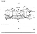
- depletion layers 140 and 141 are formed as respectively spreading from lower surfaces of the base region 114 and the trench 120 into the drain region 115 in the epitaxial layer 111 as shown in Fig. 5 .
- the depletion layer 140 spreading from the base region 114 has a relatively great width, while the depletion layer 141 spreading from the lower surface of the trench 120 has a relatively small width.
- a gate-drain capacitance CGD which is a capacitance between the gate electrode 121 and the drain region 115 is generally equal to a capacitance provided by serially coupling the capacitance of the gate insulating film 122 with the capacitance of the depletion layer 141 formed below the lower surface of the trench 120.
- the value of the capacitance of the depletion layer 141 is inversely proportional to the width of the depletion layer 141. Therefore, the depletion layer 141, if having a smaller width, has a greater capacitance value, resulting in a greater gate-drain capacitance CGD. Conversely, the depletion layer 141, if having a greater width, has a smaller capacitance value, resulting in a smaller gate-drain resistance CGD.
- Patent Document 1 Japanese Unexamined Patent Publication No. 8-250731
- the inventor of the present invention previously proposes a semiconductor device having a planar DMOSFET which ensures a reduced turn-on time to achieve a higher speed switching capability.
- the gate-drain capacitance CGD can be reduced by controlling the orientation and the width of a depletion layer in an OFF state. As a result, the turn-on time is reduced.
- the inventor of the present invention has come up with an idea that, if the art of the previous patent application is modified to be applied to a trench semiconductor device, it is possible to achieve a further higher speed switching capability with a reduced turn-on time and a lower ON resistance, and accomplished the present invention.
- a semiconductor device includes: a first epitaxial layer provided on a semiconductor substrate; a second epitaxial layer provided in contact with an upper surface of the first epitaxial layer and having a lower impurity concentration than the first epitaxial layer; a plurality of trenches provided in the second epitaxial layer as extending downward from an upper surface of the second epitaxial layer; a gate electrode embedded in each of the trenches; a source region extending downward from the upper surface of the second epitaxial layer along each of opposite side surfaces of the trench; a base region extending downward from a lower surface of the source region along each of the opposite side surfaces of the trench; and a base high concentration region provided adjacent the source region and the base region in spaced relation from the trench as extending downward from the upper surface of the second epitaxial layer to a greater depth than the base region, and having the same conductivity type as the base region and a higher impurity concentration than the base region.
- An interlayer insulating film may be provided on the gate electrode as covering a part of the upper surface of the second epitaxial layer, and a source electrode may be provided in contact with the interlayer insulating film, a part of the source region and an upper surface of the base high concentration region.
- a buried insulating film may be provided on the gate electrode to fill the trench to the vicinity of an opening edge of the trench, and a source electrode may be provided in contact with the buried insulating film, the source region and an upper surface of the base high concentration region.
- depletion layers spreading from base high concentration regions disposed on the opposite sides of the trench are merged with each other at a position below the trench when the semiconductor device is in an OFF state.
- a gate-drain capacitance CGD is reduced, thereby reducing a turn-on time.
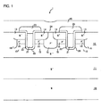
- Fig. 1 is a sectional view of a semiconductor device according to a preferred embodiment of the present invention.
- the semiconductor device 1 includes an N-type first epitaxial layer 11 provided on an N type semiconductor substrate 10 (for example, having an impurity concentration of about 10 19 /cm 3 ) and having the same conductivity type as the semiconductor substrate 10 and a lower impurity concentration (e.g., an impurity concentration of about 10 16 /cm 3 ) than the semiconductor substrate 10, and an N -- type second epitaxial layer 12 provided in contact with an upper surface of the first epitaxial layer 11 and having the same conductivity type as the first epitaxial layer 11 and a lower impurity concentration (e.g., an impurity concentration of about 10 15 /cm 3 ) than the first epitaxial layer 11.
- an impurity concentration of about 10 19 /cm 3 for example, having an impurity concentration of about 10 19 /cm 3
- a lower impurity concentration e.g., an impurity concentration of about
- the semiconductor device 101 described in BACKGROUND ART is of a single epitaxial layer structure including the epitaxial layer 111, but the semiconductor device 1 is of a double epitaxial layer structure obtained by forming the second epitaxial layer 12 on the upper surface of the first epitaxial layer 11 which corresponds to the epitaxial layer 111.
- a plurality of trenches 20 are provided in the second epitaxial layer 12 as extending downward from an upper surface of the second epitaxial layer 12.
- a MOSFET is configured along opposite side surfaces of the trenches 20. That is, a gate electrode 21 is embedded in each of the trenches 20.
- Provided along each of the opposite side surfaces of the trench are an N + type source region 13 extending downward from the upper surface of the second epitaxial layer 12 and a P - type base region 14 extending downward from a lower surface of the source region 13.
- a portion of the epitaxial layer 12 below the base region 14 and a base high concentration region 16 to be described later serves as an N -- type drain region 15.
- the base high concentration region 16 is disposed adjacent the source region 13 and the base region 14 in spaced relation from the trench 20 as extending downward from the upper surface of the second epitaxial layer 12.
- the base high concentration region 16 has the same conductivity type as the base region 14 and a higher impurity concentration than the base region 14, and is formed as extending to a greater depth than the base region 14.
- the base high concentration region 16 has an ohmic contact with a source electrode 25 to be described later, and reduces the resistance component of the base region 14. As will be described later, the base high concentration region 16 has an important function for reducing a gate-drain capacitance CGD when the semiconductor device 1 is in an OFF state.
- the source region 13, the base region 14 and the base high concentration region 16 are provided in a portion of the second epitaxial layer 12, and the rest of the second epitaxial layer 12 serves as the drain region 15.
- the first epitaxial layer 11 provided below the second epitaxial layer 12 in contact with the drain region 15 also serves as a part of the drain region.
- the second epitaxial layer 12 (drain region 15) has a low impurity concentration such that, when the semiconductor device is in the OFF state, depletion layers respectively spreading from base high concentration regions 16 disposed on opposite sides of each trench 20 are merged with each other at a position below the trench 20.
- a gate insulating film 22 of a thin silicon oxide film is provided between the trench 20 and the gate electrode 21.
- the gate insulating film 22 extends onto the upper surface of the second epitaxial layer 12.
- an interlayer insulating film 23 is provided over the gate electrode 21 and the gate insulating film 22 as covering a part of the upper surface of the second epitaxial layer 12.
- the gate insulating film 22 and the interlayer insulating film 23 each have an etched-off portion serving as a contact hole 24 on a part of the source region 13 and an upper surface of the base high concentration region 16.
- a metal layer is provided as a source electrode 25 to provide electrical contacts to the source region 13 and the base high concentration region 16 through the contact hole 24. Therefore, the source electrode 25 (mechanically) contacts the interlayer insulating film 23, the part of the source region 13 and the upper surface of the base high concentration region 16.
- the first epitaxial layer 11 is formed on the semiconductor substrate 10 by an epitaxial technique
- the second epitaxial layer 12 is formed on the first epitaxial layer 11 by an epitaxial technique
- the base high concentration region 16 is formed as extending to a greater depth than the base region 41 by an impurity diffusion technique or an impurity implantation technique.
- the semiconductor device 1 is in the ON state when a gate-source voltage VGS which is a voltage between the gate electrodes 21 and the source electrode 25 is not less than a threshold, and is in the OFF state when the gate-source voltage VGS is less than the threshold.
- VGS gate-source voltage
- the ON state channel layers are formed in the base regions 14, so that ON electric current flows from the semiconductor substrate 10 to the source electrode 25 through the first epitaxial layer 11, the drain region 15, the base regions 14 and the source regions 13.
- a drain-source voltage VDS which is a voltage between the semiconductor substrate 10 and the source electrode 25 is generally reduced.
- the drain-source voltage VDS is higher (e.g., 20V), so that the depletion layers 40 occur as shown in Fig. 2 .
- the base high concentration region 16 is formed as having a greater depth and a higher impurity concentration than the base region 14 and, therefore, a depletion layer 40 spreading depthwise and laterally from the base high concentration region 16 fills the drain region 15 having a very low impurity concentration to extend into an inner portion of the first epitaxial layer 11. That is, the depletion layers 40 spreading from the base high concentration regions 16 disposed on the opposite sides of each trench 20 are merged with each other below the trench 20. Depletion layers spreading from lower surfaces of the base region 14 and the trench 20 are completely contained in and integrated with the depletion layers 40 widely spreading from the base high concentration regions 16.
- the depletion layer 40 present below the lower surface of the trench 20 has a greater width, so that the depletion layer portion has a smaller capacitance value. Since the gate-drain capacitance CGD is equal to a capacitance obtained by serially coupling the capacitance of the gate insulating film 22 and the capacitance of the depletion layer portion formed below the lower surface of the trench 20 as described above, the gate-drain capacitance CGD is reduced. As a result, the semiconductor device 1 has a reduced turn-on time, thereby achieving higher speed switching.
- the width of the depletion layer portion present below the lower surface of the trench 20 is increased and, therefore, the gate-drain capacitance CGD is reduced.
- the drain region 15 in the second epitaxial layer 12 has a higher resistivity. Therefore, if the distance from the lower surface of the trench 20 to the upper surface of the first epitaxial layer 11 is increased, the semiconductor device 1 is liable to have an increased ON resistance in the ON state. Therefore, it is necessary to determine the distance from the lower surface of the trench 20 to the upper surface of the first epitaxial layer 11 so that the resulting ON resistance is within a permissible range.
- Fig. 3 is a sectional view of the semiconductor device 2.
- the semiconductor device 2 includes a semiconductor substrate 10, a first epitaxial layer 11 and a second epitaxial layer 12.
- Source regions 13, base regions 14, base high concentration regions 16 and a drain region 15 are provided in the second epitaxial layer 12.
- Gate electrodes 21 are respectively embedded in trenches 20 provided in the second epitaxial layer 12.
- buried insulating films 26 are respectively provided on the gate electrodes 21 to fill the trenches to the vicinities of opening edges of the trenches 20 for isolation between the gate electrodes 21 and the source electrodes 25.
- a source electrode 25 is provided over and in contact with upper surfaces of the buried insulating films 26, the source regions 13 and the base high concentration regions 16.
- the buried insulating films 26 of the semiconductor device 2 are provided at a level not higher than the upper surface of the second epitaxial layer 12. Therefore, there is no need to provide contact holes for electrically contacting the source electrode 25 to the source regions 13 and the base high concentration regions 16. As a result, microminiaturization can be achieved to locate the base high concentration regions 16 closer to the trenches 20. Therefore, even if the impurity concentration of the second epitaxial layer 12 is higher than in the semiconductor device 1, depletion layers 40 spreading from the base high concentration regions 16 disposed on opposite sides of each trench 20 are merged with each other at a position below the trench 20. Thus, the drain region 15 in the second epitaxial layer 12 is permitted to have a relatively low resistivity, thereby suppressing an increase in ON resistance.
- the MOSFET configured along the side surfaces of the trenches is of the N type in the embodiments, but may be of a P type with the conductivity types of the respective regions being reversed.
Landscapes
- Electrodes Of Semiconductors (AREA)
- Thyristors (AREA)
Abstract
A trench semiconductor device is provided which ensures a reduced turn-on time. The semiconductor device (1) includes: a first epitaxial layer provided on a semiconductor substrate; a second epitaxial layer provided in contact with an upper surface of the first epitaxial layer and having a lower impurity concentration than the first epitaxial layer; a plurality of trenches provided in the second epitaxial layer as extending downward from an upper surface of the second epitaxial layer; a gate electrode embedded in each of the trenches; a source region extending downward from the upper surface of the second epitaxial layer along each of opposite side surfaces of the trench; a base region extending downward from a lower surface of the source region along each of the opposite side surfaces of the trench; and a base high concentration region provided adjacent the source region and the base region in spaced relation from the trench as extending downward from the upper surface of the second epitaxial layer to a greater depth than the base region, and having the same conductivity type as the base region and a higher impurity concentration than the base region.
Description
- The present invention relates to a semiconductor device and, particularly, to a semiconductor device including a MOSFET configured along side surfaces of trenches.
- In recent years, there has been an increasing demand for a semiconductor device including a MOSFET configured along side surfaces of trenches (hereinafter referred to as "trench semiconductor device"), because this semiconductor device has a lower ON resistance than a semiconductor device including a MOSFET (planar DMOSFET (double diffused MOSFET)) configured along an upper surface of an epitaxial layer.
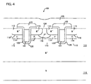
- A conventional trench semiconductor device is shown in
Fig. 4 . Thesemiconductor device 101 includes an N- typeepitaxial layer 111 provided on an upper surface of an Ntype semiconductor substrate 110. A plurality of trenches (grooves) 120 are provided in theepitaxial layer 111 as extending downward from an upper surface of theepitaxial layer 111. A MOSFET is configured along opposite side surfaces of thetrenches 120. - That is, a
gate electrode 121 is embedded in each of the trenches, and an N+type source region 113 and a P-type base region 114 are arranged in this order toward a lower side along each of the opposite side surfaces of thetrenches 120. A portion of theepitaxial layer 111 below thebase region 114 serves as an N-type drain region 115. A basehigh concentration region 116 is provided adjacent thesource region 113 and thebase region 114 in spaced relation from thetrench 120 as extending downward from the upper surface of theepitaxial layer 111. The basehigh concentration region 116 has the same conductivity type as thebase region 114 and a higher impurity concentration than thebase region 114, and is shallower than thebase region 114. The basehigh concentration region 116 has an ohmic contact with asource electrode 125 to be described later, and reduces the resistance component of thebase region 114. - A gate
insulating film 122 of a thin silicon oxide film is provided between thetrench 120 and thegate electrode 121. Thegate insulating film 122 extends onto the upper surface of theepitaxial layer 111. Further, an interlayerinsulating film 123 is provided on the gate electrode and thegate insulating film 22 as partly covering the upper surface of theepitaxial layer 111. Thegate insulating film 122 and theinterlayer insulating film 123 each have an etched-off portion serving as acontact hole 124 on a part of thesource region 113 and an upper surface of the basehigh concentration region 116. A metal layer is provided as thesource electrode 125 to provide electrical contacts to thesource region 113 and the basehigh concentration region 116 through thecontact hole 124. - Where the
semiconductor device 101 is in an OFF state,depletion layers base region 114 and thetrench 120 into thedrain region 115 in theepitaxial layer 111 as shown inFig. 5 . Thedepletion layer 140 spreading from thebase region 114 has a relatively great width, while thedepletion layer 141 spreading from the lower surface of thetrench 120 has a relatively small width. A gate-drain capacitance CGD which is a capacitance between thegate electrode 121 and thedrain region 115 is generally equal to a capacitance provided by serially coupling the capacitance of thegate insulating film 122 with the capacitance of thedepletion layer 141 formed below the lower surface of thetrench 120. The value of the capacitance of thedepletion layer 141 is inversely proportional to the width of thedepletion layer 141. Therefore, thedepletion layer 141, if having a smaller width, has a greater capacitance value, resulting in a greater gate-drain capacitance CGD. Conversely, thedepletion layer 141, if having a greater width, has a smaller capacitance value, resulting in a smaller gate-drain resistance CGD.
Patent Document 1:Japanese Unexamined Patent Publication No. 8-250731 - Meanwhile, in
Japanese Patent Application No. 2005-115952 - The inventor of the present invention has come up with an idea that, if the art of the previous patent application is modified to be applied to a trench semiconductor device, it is possible to achieve a further higher speed switching capability with a reduced turn-on time and a lower ON resistance, and accomplished the present invention.
- In view of the foregoing, it is an object of the present invention to provide a trench semiconductor device which ensures a reduced turn-on time.
- A semiconductor device according to the present invention includes: a first epitaxial layer provided on a semiconductor substrate; a second epitaxial layer provided in contact with an upper surface of the first epitaxial layer and having a lower impurity concentration than the first epitaxial layer; a plurality of trenches provided in the second epitaxial layer as extending downward from an upper surface of the second epitaxial layer; a gate electrode embedded in each of the trenches; a source region extending downward from the upper surface of the second epitaxial layer along each of opposite side surfaces of the trench; a base region extending downward from a lower surface of the source region along each of the opposite side surfaces of the trench; and a base high concentration region provided adjacent the source region and the base region in spaced relation from the trench as extending downward from the upper surface of the second epitaxial layer to a greater depth than the base region, and having the same conductivity type as the base region and a higher impurity concentration than the base region.
- An interlayer insulating film may be provided on the gate electrode as covering a part of the upper surface of the second epitaxial layer, and a source electrode may be provided in contact with the interlayer insulating film, a part of the source region and an upper surface of the base high concentration region.
- Alternatively, a buried insulating film may be provided on the gate electrode to fill the trench to the vicinity of an opening edge of the trench, and a source electrode may be provided in contact with the buried insulating film, the source region and an upper surface of the base high concentration region.
- According to the inventive semiconductor device, depletion layers spreading from base high concentration regions disposed on the opposite sides of the trench are merged with each other at a position below the trench when the semiconductor device is in an OFF state. As a result, a gate-drain capacitance CGD is reduced, thereby reducing a turn-on time.
- The foregoing and other objects, features and effects of the present invention will become more apparent from the following description of the preferred embodiments with reference to the attached drawings.
-
-
Fig. 1 is a sectional view of a semiconductor device according to a preferred embodiment of the present invention. -
Fig. 2 is a sectional view illustrating an OFF state of the semiconductor device. -
Fig. 3 is a sectional view of a semiconductor device according to another preferred embodiment of the present invention. -
Fig. 4 is a sectional view of a conventional semiconductor device. -
Fig. 5 is a sectional view illustrating an OFF state of the conventional semiconductor device. - The best mode for carrying out the invention will hereinafter be described with reference to the drawings.
-
Fig. 1 is a sectional view of a semiconductor device according to a preferred embodiment of the present invention. The semiconductor device 1 includes an N-type firstepitaxial layer 11 provided on an N type semiconductor substrate 10 (for example, having an impurity concentration of about 1019/cm3) and having the same conductivity type as thesemiconductor substrate 10 and a lower impurity concentration (e.g., an impurity concentration of about 1016/cm3) than thesemiconductor substrate 10, and an N-- type secondepitaxial layer 12 provided in contact with an upper surface of the firstepitaxial layer 11 and having the same conductivity type as the firstepitaxial layer 11 and a lower impurity concentration (e.g., an impurity concentration of about 1015/cm3) than the firstepitaxial layer 11. That is, thesemiconductor device 101 described in BACKGROUND ART is of a single epitaxial layer structure including theepitaxial layer 111, but the semiconductor device 1 is of a double epitaxial layer structure obtained by forming the secondepitaxial layer 12 on the upper surface of the firstepitaxial layer 11 which corresponds to theepitaxial layer 111. - A plurality of
trenches 20 are provided in the secondepitaxial layer 12 as extending downward from an upper surface of the secondepitaxial layer 12. A MOSFET is configured along opposite side surfaces of thetrenches 20. That is, agate electrode 21 is embedded in each of thetrenches 20. Provided along each of the opposite side surfaces of the trench are an N+type source region 13 extending downward from the upper surface of the secondepitaxial layer 12 and a P-type base region 14 extending downward from a lower surface of thesource region 13. A portion of theepitaxial layer 12 below thebase region 14 and a basehigh concentration region 16 to be described later serves as an N--type drain region 15. The basehigh concentration region 16 is disposed adjacent thesource region 13 and thebase region 14 in spaced relation from thetrench 20 as extending downward from the upper surface of the secondepitaxial layer 12. The basehigh concentration region 16 has the same conductivity type as thebase region 14 and a higher impurity concentration than thebase region 14, and is formed as extending to a greater depth than thebase region 14. The basehigh concentration region 16 has an ohmic contact with asource electrode 25 to be described later, and reduces the resistance component of thebase region 14. As will be described later, the basehigh concentration region 16 has an important function for reducing a gate-drain capacitance CGD when the semiconductor device 1 is in an OFF state. - Thus, the
source region 13, thebase region 14 and the basehigh concentration region 16 are provided in a portion of the secondepitaxial layer 12, and the rest of the secondepitaxial layer 12 serves as thedrain region 15. The firstepitaxial layer 11 provided below the secondepitaxial layer 12 in contact with thedrain region 15 also serves as a part of the drain region. As will be described later, the second epitaxial layer 12 (drain region 15) has a low impurity concentration such that, when the semiconductor device is in the OFF state, depletion layers respectively spreading from basehigh concentration regions 16 disposed on opposite sides of eachtrench 20 are merged with each other at a position below thetrench 20. - As in the
semiconductor device 101 described in BACKGROUND ART, agate insulating film 22 of a thin silicon oxide film is provided between thetrench 20 and thegate electrode 21. Thegate insulating film 22 extends onto the upper surface of the secondepitaxial layer 12. Further, an interlayerinsulating film 23 is provided over thegate electrode 21 and thegate insulating film 22 as covering a part of the upper surface of the secondepitaxial layer 12. Thegate insulating film 22 and theinterlayer insulating film 23 each have an etched-off portion serving as acontact hole 24 on a part of thesource region 13 and an upper surface of the basehigh concentration region 16. A metal layer is provided as asource electrode 25 to provide electrical contacts to thesource region 13 and the basehigh concentration region 16 through thecontact hole 24. Therefore, the source electrode 25 (mechanically) contacts theinterlayer insulating film 23, the part of thesource region 13 and the upper surface of the basehigh concentration region 16. - Although a production method for the semiconductor device 1 will not be described, features of the production method are that the
first epitaxial layer 11 is formed on thesemiconductor substrate 10 by an epitaxial technique, that thesecond epitaxial layer 12 is formed on thefirst epitaxial layer 11 by an epitaxial technique, and that the basehigh concentration region 16 is formed as extending to a greater depth than thebase region 41 by an impurity diffusion technique or an impurity implantation technique. - Next, ON and OFF states of the semiconductor device 1 will be described. The semiconductor device 1 is in the ON state when a gate-source voltage VGS which is a voltage between the
gate electrodes 21 and thesource electrode 25 is not less than a threshold, and is in the OFF state when the gate-source voltage VGS is less than the threshold. In the ON state, channel layers are formed in thebase regions 14, so that ON electric current flows from thesemiconductor substrate 10 to thesource electrode 25 through thefirst epitaxial layer 11, thedrain region 15, thebase regions 14 and thesource regions 13. As a result, a drain-source voltage VDS which is a voltage between thesemiconductor substrate 10 and thesource electrode 25 is generally reduced. - In the OFF state, on the other hand, the drain-source voltage VDS is higher (e.g., 20V), so that the depletion layers 40 occur as shown in
Fig. 2 . It should be herein noted that the basehigh concentration region 16 is formed as having a greater depth and a higher impurity concentration than thebase region 14 and, therefore, adepletion layer 40 spreading depthwise and laterally from the basehigh concentration region 16 fills thedrain region 15 having a very low impurity concentration to extend into an inner portion of thefirst epitaxial layer 11. That is, the depletion layers 40 spreading from the basehigh concentration regions 16 disposed on the opposite sides of eachtrench 20 are merged with each other below thetrench 20. Depletion layers spreading from lower surfaces of thebase region 14 and thetrench 20 are completely contained in and integrated with the depletion layers 40 widely spreading from the basehigh concentration regions 16. - Therefore, a portion of the
depletion layer 40 present below the lower surface of thetrench 20 has a greater width, so that the depletion layer portion has a smaller capacitance value. Since the gate-drain capacitance CGD is equal to a capacitance obtained by serially coupling the capacitance of thegate insulating film 22 and the capacitance of the depletion layer portion formed below the lower surface of thetrench 20 as described above, the gate-drain capacitance CGD is reduced. As a result, the semiconductor device 1 has a reduced turn-on time, thereby achieving higher speed switching. - In this case, as a distance from the lower surface of the
trench 20 to the upper surface of thefirst epitaxial layer 11 increases, the width of the depletion layer portion present below the lower surface of thetrench 20 is increased and, therefore, the gate-drain capacitance CGD is reduced. However, it should be noted that thedrain region 15 in thesecond epitaxial layer 12 has a higher resistivity. Therefore, if the distance from the lower surface of thetrench 20 to the upper surface of thefirst epitaxial layer 11 is increased, the semiconductor device 1 is liable to have an increased ON resistance in the ON state. Therefore, it is necessary to determine the distance from the lower surface of thetrench 20 to the upper surface of thefirst epitaxial layer 11 so that the resulting ON resistance is within a permissible range. - Next, a semiconductor device according to another preferred embodiment of the present invention will be described.
Fig. 3 is a sectional view of thesemiconductor device 2. Like the semiconductor device 1, thesemiconductor device 2 includes asemiconductor substrate 10, afirst epitaxial layer 11 and asecond epitaxial layer 12.Source regions 13,base regions 14, basehigh concentration regions 16 and adrain region 15 are provided in thesecond epitaxial layer 12.Gate electrodes 21 are respectively embedded intrenches 20 provided in thesecond epitaxial layer 12. Further, buried insulatingfilms 26 are respectively provided on thegate electrodes 21 to fill the trenches to the vicinities of opening edges of thetrenches 20 for isolation between thegate electrodes 21 and thesource electrodes 25. Asource electrode 25 is provided over and in contact with upper surfaces of the buried insulatingfilms 26, thesource regions 13 and the basehigh concentration regions 16. - Unlike the
interlayer insulating film 23 of the semiconductor device 1, the buried insulatingfilms 26 of thesemiconductor device 2 are provided at a level not higher than the upper surface of thesecond epitaxial layer 12. Therefore, there is no need to provide contact holes for electrically contacting thesource electrode 25 to thesource regions 13 and the basehigh concentration regions 16. As a result, microminiaturization can be achieved to locate the basehigh concentration regions 16 closer to thetrenches 20. Therefore, even if the impurity concentration of thesecond epitaxial layer 12 is higher than in the semiconductor device 1, depletion layers 40 spreading from the basehigh concentration regions 16 disposed on opposite sides of eachtrench 20 are merged with each other at a position below thetrench 20. Thus, thedrain region 15 in thesecond epitaxial layer 12 is permitted to have a relatively low resistivity, thereby suppressing an increase in ON resistance. - The present invention is not limited to the embodiments described above, but any of various design modifications may be made within the purview defined by the claims. For example, the MOSFET configured along the side surfaces of the trenches is of the N type in the embodiments, but may be of a P type with the conductivity types of the respective regions being reversed.
- While the embodiments of the present invention have been described in detail, it should be understood that these embodiments are merely illustrative of the technical principles of the present invention but not limitative of the invention. The spirit and scope of the present invention are to be limited only by the appended claims.
- This application corresponds to
Japanese Patent Application No. 2005-173243
Claims (3)
- A semiconductor device comprising:a first epitaxial layer provided on a semiconductor substrate;a second epitaxial layer provided in contact with an upper surface of the first epitaxial layer and having a lower impurity concentration than the first epitaxial layer;a plurality of trenches provided in the second epitaxial layer as extending downward from an upper surface of the second epitaxial layer;a gate electrode embedded in each of the trenches;a source region extending downward from the upper surface of the second epitaxial layer along each of opposite side surfaces of the trench;a base region extending downward from a lower surface of the source region along each of the opposite side surfaces of the trench; anda base high concentration region provided adjacent the source region and the base region in spaced relation from the trench as extending downward from the upper surface of the second epitaxial layer to a greater depth than the base region, and having the same conductivity type as the base region and a higher impurity concentration than the base region.
- The semiconductor device according to claim 1,
wherein an interlayer insulating film is provided on the gate electrode as covering a part of the upper surface of the second epitaxial layer,
wherein a source electrode is provided in contact with the interlayer insulating film, a part of the source region and an upper surface of the base high concentration region. - The semiconductor device according to claim 1,
wherein a buried insulating film is provided on the gate electrode to fill the trench to the vicinity of an opening edge of the trench,
wherein a source electrode is provided in contact with the buried insulating film, the source region and an upper surface of the base high concentration region.
Applications Claiming Priority (2)
| Application Number | Priority Date | Filing Date | Title |
|---|---|---|---|
| JP2005173243A JP5008046B2 (en) | 2005-06-14 | 2005-06-14 | Semiconductor device |
| PCT/JP2006/311420 WO2006134810A1 (en) | 2005-06-14 | 2006-06-07 | Semiconductor device |
Publications (2)
| Publication Number | Publication Date |
|---|---|
| EP1909330A1 true EP1909330A1 (en) | 2008-04-09 |
| EP1909330A4 EP1909330A4 (en) | 2009-12-09 |
Family
ID=37532173
Family Applications (1)
| Application Number | Title | Priority Date | Filing Date |
|---|---|---|---|
| EP06757127A Withdrawn EP1909330A4 (en) | 2005-06-14 | 2006-06-07 | SEMICONDUCTOR DEVICE |
Country Status (7)
| Country | Link |
|---|---|
| US (1) | US7939884B2 (en) |
| EP (1) | EP1909330A4 (en) |
| JP (1) | JP5008046B2 (en) |
| KR (1) | KR20080014855A (en) |
| CN (1) | CN101194366A (en) |
| TW (1) | TW200731535A (en) |
| WO (1) | WO2006134810A1 (en) |
Families Citing this family (9)
| Publication number | Priority date | Publication date | Assignee | Title |
|---|---|---|---|---|
| JP5189771B2 (en) * | 2007-02-01 | 2013-04-24 | ローム株式会社 | GaN-based semiconductor devices |
| JP4564514B2 (en) | 2007-05-18 | 2010-10-20 | 株式会社東芝 | Semiconductor device |
| KR100853799B1 (en) | 2007-07-25 | 2008-08-25 | 주식회사 동부하이텍 | Trench gate semiconductor device and manufacturing method thereof |
| JP2009038318A (en) * | 2007-08-03 | 2009-02-19 | Toshiba Corp | Semiconductor device |
| JP2010045123A (en) * | 2008-08-11 | 2010-02-25 | Mitsubishi Electric Corp | Semiconductor device and method of manufacturing the same |
| JP6047297B2 (en) * | 2012-04-09 | 2016-12-21 | ルネサスエレクトロニクス株式会社 | Semiconductor device |
| US9954072B2 (en) | 2012-10-18 | 2018-04-24 | Mitsubishi Electric Corporation | Silicon-carbide semiconductor device and manufacturing method thereof |
| US20160013300A1 (en) * | 2013-02-25 | 2016-01-14 | Hitachi, Ltd. | Semiconductor device, drive device for semiconductor circuit, and power conversion device |
| US10446497B2 (en) * | 2016-03-29 | 2019-10-15 | Microchip Technology Incorporated | Combined source and base contact for a field effect transistor |
Family Cites Families (45)
| Publication number | Priority date | Publication date | Assignee | Title |
|---|---|---|---|---|
| BE754567A (en) | 1969-08-09 | 1971-02-08 | Basf Ag | IRRADIATION CURABLE MATERIALS, BASED ON POLYMERS WITH NON-SATURATED ETHYLENICALLY REPEATED GROUPS |
| US3999946A (en) | 1976-02-23 | 1976-12-28 | Allied Chemical Corporation | Time-temperature history indicators |
| US4215208A (en) | 1977-10-05 | 1980-07-29 | Allied Chemical Corporation | Thermochromic polyacetylenes containing urethane groups |
| US4238352A (en) | 1978-11-13 | 1980-12-09 | Allied Chemical Corporation | Co-polymerized acetylenic compositions |
| US4242440A (en) | 1979-04-30 | 1980-12-30 | Allied Chemical Corporation | Thermochromic polyacetylenes used in laser beam recording method |
| US4389217A (en) | 1979-05-11 | 1983-06-21 | Allied Corporation | Integrated time-temperature or radiation-dosage history recording device |
| US4708019A (en) | 1984-06-27 | 1987-11-24 | Gte Laboratories Incorporated | Measurement of strain employing a piezoresistive blend of a doped acetylene polymer and an elastomer |
| US4767826A (en) | 1985-07-18 | 1988-08-30 | Polytechnic Institute Of New York | Radiation-sensitive polymers |
| US4721769A (en) | 1985-10-18 | 1988-01-26 | Gte Laboratories Incorporated | Diacetylene segmented copolymers |
| US4916211A (en) | 1986-03-07 | 1990-04-10 | Gte Laboratories Incorporated | Thermochromic cross polymerized polyamide-diacetylene compound |
| US4849500A (en) | 1986-03-07 | 1989-07-18 | Gte Laboratories Incorporated | Polyamide from diacetylene dicarboxylic acid compound |
| JP2941823B2 (en) * | 1988-11-28 | 1999-08-30 | 株式会社日立製作所 | Semiconductor device and manufacturing method thereof |
| US5156810A (en) | 1989-06-15 | 1992-10-20 | Biocircuits Corporation | Biosensors employing electrical, optical and mechanical signals |
| US5491097A (en) | 1989-06-15 | 1996-02-13 | Biocircuits Corporation | Analyte detection with multilayered bioelectronic conductivity sensors |
| US5672465A (en) | 1990-04-09 | 1997-09-30 | Jp Laboratories, Inc. | Polyethyleneimine binder complex films |
| GB9215653D0 (en) | 1992-07-23 | 1992-09-09 | Philips Electronics Uk Ltd | A method of manufacturing a semiconductor device comprising an insulated gate field effect device |
| US5910669A (en) * | 1992-07-24 | 1999-06-08 | Siliconix Incorporated | Field effect Trench transistor having lightly doped epitaxial region on the surface portion thereof |
| US5558313A (en) * | 1992-07-24 | 1996-09-24 | Siliconix Inorporated | Trench field effect transistor with reduced punch-through susceptibility and low RDSon |
| US6468759B1 (en) | 1997-03-03 | 2002-10-22 | Regents Of The University Of California | Direct colorimetric detection of biocatalysts |
| US6022748A (en) | 1997-08-29 | 2000-02-08 | Sandia Corporation - New Mexico Regents Of The University Of California | Sol-gel matrices for direct colorimetric detection of analytes |
| US5554686A (en) | 1993-08-20 | 1996-09-10 | Minnesota Mining And Manufacturing Company | Room temperature curable silane-terminated polyurethane dispersions |
| US6103217A (en) | 1994-08-11 | 2000-08-15 | The Regents Of The University Of California | Polymeric assemblies for sensitive colorimetric assays |
| US5674766A (en) * | 1994-12-30 | 1997-10-07 | Siliconix Incorporated | Method of making a trench MOSFET with multi-resistivity drain to provide low on-resistance by varying dopant concentration in epitaxial layer |
| AU714839B2 (en) | 1995-02-13 | 2000-01-13 | Regents Of The University Of California, The | Three-dimensional colorimetric assay assemblies |
| JPH08264772A (en) * | 1995-03-23 | 1996-10-11 | Toyota Motor Corp | Field effect semiconductor device |
| JPH08316468A (en) * | 1995-05-22 | 1996-11-29 | Hitachi Ltd | Semiconductor wafer, semiconductor device and manufacturing method thereof |
| US5616400A (en) | 1995-11-20 | 1997-04-01 | Century International Adhesives & Coating Corporation | Cold seal adhesives, cold sealable films and packages formed therewith |
| US5685641A (en) | 1996-01-16 | 1997-11-11 | Ribi; Hans O. | Devices for rapid temperature detection |
| IL125517A0 (en) | 1996-01-26 | 1999-03-12 | Univ California | Polymeric film assay and method for direct colorimetric detection of analytes |
| US5770878A (en) * | 1996-04-10 | 1998-06-23 | Harris Corporation | Trench MOS gate device |
| WO1998004743A1 (en) | 1996-07-29 | 1998-02-05 | The Regents Of The University Of California | Polymeric assemblies for sensitive colorimetric assays |
| EP1007943A1 (en) | 1997-02-14 | 2000-06-14 | The Regents Of The University Of California | Protein-coupled colorimetric analyte detectors |
| US5929160A (en) | 1997-09-25 | 1999-07-27 | Minnesota Mining And Manufacturing Company | Method for reducing water uptake in silyl terminated sulfopoly(ester-urethanes) |
| EP1112377A4 (en) | 1998-06-22 | 2004-11-10 | Univ California | COLORIMETRIC DETECTORS OF SUBSTANCES FOR ANALYSIS COUPLED WITH NUCLEIC ACIDS |
| JP3358611B2 (en) * | 2000-01-19 | 2002-12-24 | 日本電気株式会社 | Method for manufacturing semiconductor device |
| US6518359B1 (en) | 2000-02-25 | 2003-02-11 | 3M Innovative Properties Co. | Polyurethane-based pressure-sensitive adhesives, systems for such adhesives, articles therefrom, and methods of making |
| US6642304B1 (en) | 2000-02-25 | 2003-11-04 | 3M Innovative Properties Company | Polyurethane-based adhesives, systems for such adhesives, articles therefrom, and methods of making |
| US6580123B2 (en) * | 2000-04-04 | 2003-06-17 | International Rectifier Corporation | Low voltage power MOSFET device and process for its manufacture |
| US6607744B1 (en) | 2000-06-23 | 2003-08-19 | Segan Industries | Ingestibles possessing intrinsic color change |
| US6963007B2 (en) | 2002-12-19 | 2005-11-08 | 3M Innovative Properties Company | Diacetylenic materials for sensing applications |
| US20040126897A1 (en) | 2002-12-19 | 2004-07-01 | 3M Innovative Properties Company | Colorimetric sensors constructed of diacetylene materials |
| JP4618766B2 (en) | 2003-10-01 | 2011-01-26 | ローム株式会社 | Semiconductor device |
| US20050137375A1 (en) | 2003-12-19 | 2005-06-23 | 3M Innovative Properties Company | Polyurethane-based pressure sensitive adhesives and methods of manufacture |
| US7371511B2 (en) | 2004-08-19 | 2008-05-13 | 3M Innovative Properties Company | Polydiacetylene polymer blends |
| BRPI0519119A2 (en) | 2004-12-17 | 2008-12-23 | 3M Innovative Properties Co | colorimetric system and method for detecting an analyte |
-
2005
- 2005-06-14 JP JP2005173243A patent/JP5008046B2/en not_active Expired - Fee Related
-
2006
- 2006-06-07 CN CNA200680020893XA patent/CN101194366A/en active Pending
- 2006-06-07 KR KR1020077028959A patent/KR20080014855A/en not_active Withdrawn
- 2006-06-07 EP EP06757127A patent/EP1909330A4/en not_active Withdrawn
- 2006-06-07 WO PCT/JP2006/311420 patent/WO2006134810A1/en not_active Ceased
- 2006-06-07 US US11/922,092 patent/US7939884B2/en active Active
- 2006-06-14 TW TW095121226A patent/TW200731535A/en unknown
Also Published As
| Publication number | Publication date |
|---|---|
| US7939884B2 (en) | 2011-05-10 |
| KR20080014855A (en) | 2008-02-14 |
| WO2006134810A1 (en) | 2006-12-21 |
| EP1909330A4 (en) | 2009-12-09 |
| TW200731535A (en) | 2007-08-16 |
| US20090302379A1 (en) | 2009-12-10 |
| JP5008046B2 (en) | 2012-08-22 |
| JP2006351652A (en) | 2006-12-28 |
| CN101194366A (en) | 2008-06-04 |
Similar Documents
| Publication | Publication Date | Title |
|---|---|---|
| US11114558B2 (en) | Shielded gate trench MOSFET integrated with super barrier rectifier | |
| US8049270B2 (en) | Semiconductor device | |
| KR100652449B1 (en) | Horizontal Thin Film Silicon-On-Insulators | |
| US6008520A (en) | Trench MOSFET with heavily doped delta layer to provide low on- resistance | |
| US5688725A (en) | Method of making a trench mosfet with heavily doped delta layer to provide low on-resistance | |
| US7064384B2 (en) | Semiconductor device | |
| US11257944B2 (en) | Semiconductor device and semiconductor device manufacturing method | |
| US7126166B2 (en) | High voltage lateral FET structure with improved on resistance performance | |
| US5804864A (en) | High withstand voltage semiconductor device and manufacturing method thereof | |
| US7906808B2 (en) | Semiconductor device | |
| EP1256985A2 (en) | Lateral power MISFET | |
| US20150380545A1 (en) | Power semiconductor device | |
| US10468520B2 (en) | Switching element and method of manufacturing the same | |
| CN107026207B (en) | Semiconductor device including lateral transistor | |
| CN101800243A (en) | Trench dmos transistor having a double gate structure | |
| US12439620B2 (en) | Semiconductor device | |
| JP2017195224A (en) | Switching element | |
| US7939884B2 (en) | Semiconductor device | |
| CN106783973A (en) | High voltage integrated circuit with the conduction resistance value for improving and the breakdown voltage of improvement | |
| US10367091B2 (en) | Semiconductor switching element | |
| EP1870940A1 (en) | Semiconductor device | |
| JP7135819B2 (en) | semiconductor equipment | |
| US20240170548A1 (en) | Semiconductor device and method of manufacturing the same | |
| CN116978946A (en) | Silicon-on-insulator lateral device and manufacturing method thereof | |
| HK1014805A (en) | Trench mosfet with heavily doped delta-layer to provide low on-resistance |
Legal Events
| Date | Code | Title | Description |
|---|---|---|---|
| PUAI | Public reference made under article 153(3) epc to a published international application that has entered the european phase |
Free format text: ORIGINAL CODE: 0009012 |
|
| 17P | Request for examination filed |
Effective date: 20080110 |
|
| AK | Designated contracting states |
Kind code of ref document: A1 Designated state(s): DE FR GB |
|
| RBV | Designated contracting states (corrected) |
Designated state(s): DE FR GB |
|
| DAX | Request for extension of the european patent (deleted) | ||
| A4 | Supplementary search report drawn up and despatched |
Effective date: 20091106 |
|
| 17Q | First examination report despatched |
Effective date: 20100212 |
|
| STAA | Information on the status of an ep patent application or granted ep patent |
Free format text: STATUS: THE APPLICATION IS DEEMED TO BE WITHDRAWN |
|
| 18D | Application deemed to be withdrawn |
Effective date: 20100623 |