EP1909133A2 - Array substrate, display panel having the same and method of manufacturing the same - Google Patents
Array substrate, display panel having the same and method of manufacturing the same Download PDFInfo
- Publication number
- EP1909133A2 EP1909133A2 EP07018164A EP07018164A EP1909133A2 EP 1909133 A2 EP1909133 A2 EP 1909133A2 EP 07018164 A EP07018164 A EP 07018164A EP 07018164 A EP07018164 A EP 07018164A EP 1909133 A2 EP1909133 A2 EP 1909133A2
- Authority
- EP
- European Patent Office
- Prior art keywords
- color filter
- electrode
- pixel
- array substrate
- thin film
- Prior art date
- Legal status (The legal status is an assumption and is not a legal conclusion. Google has not performed a legal analysis and makes no representation as to the accuracy of the status listed.)
- Granted
Links
Images




Classifications
-
- G—PHYSICS
- G02—OPTICS
- G02F—OPTICAL DEVICES OR ARRANGEMENTS FOR THE CONTROL OF LIGHT BY MODIFICATION OF THE OPTICAL PROPERTIES OF THE MEDIA OF THE ELEMENTS INVOLVED THEREIN; NON-LINEAR OPTICS; FREQUENCY-CHANGING OF LIGHT; OPTICAL LOGIC ELEMENTS; OPTICAL ANALOGUE/DIGITAL CONVERTERS
- G02F1/00—Devices or arrangements for the control of the intensity, colour, phase, polarisation or direction of light arriving from an independent light source, e.g. switching, gating or modulating; Non-linear optics
- G02F1/01—Devices or arrangements for the control of the intensity, colour, phase, polarisation or direction of light arriving from an independent light source, e.g. switching, gating or modulating; Non-linear optics for the control of the intensity, phase, polarisation or colour
- G02F1/13—Devices or arrangements for the control of the intensity, colour, phase, polarisation or direction of light arriving from an independent light source, e.g. switching, gating or modulating; Non-linear optics for the control of the intensity, phase, polarisation or colour based on liquid crystals, e.g. single liquid crystal display cells
- G02F1/133—Constructional arrangements; Operation of liquid crystal cells; Circuit arrangements
- G02F1/136—Liquid crystal cells structurally associated with a semi-conducting layer or substrate, e.g. cells forming part of an integrated circuit
- G02F1/1362—Active matrix addressed cells
- G02F1/136209—Light shielding layers, e.g. black matrix, incorporated in the active matrix substrate, e.g. structurally associated with the switching element
-
- G—PHYSICS
- G02—OPTICS
- G02F—OPTICAL DEVICES OR ARRANGEMENTS FOR THE CONTROL OF LIGHT BY MODIFICATION OF THE OPTICAL PROPERTIES OF THE MEDIA OF THE ELEMENTS INVOLVED THEREIN; NON-LINEAR OPTICS; FREQUENCY-CHANGING OF LIGHT; OPTICAL LOGIC ELEMENTS; OPTICAL ANALOGUE/DIGITAL CONVERTERS
- G02F1/00—Devices or arrangements for the control of the intensity, colour, phase, polarisation or direction of light arriving from an independent light source, e.g. switching, gating or modulating; Non-linear optics
- G02F1/01—Devices or arrangements for the control of the intensity, colour, phase, polarisation or direction of light arriving from an independent light source, e.g. switching, gating or modulating; Non-linear optics for the control of the intensity, phase, polarisation or colour
- G02F1/13—Devices or arrangements for the control of the intensity, colour, phase, polarisation or direction of light arriving from an independent light source, e.g. switching, gating or modulating; Non-linear optics for the control of the intensity, phase, polarisation or colour based on liquid crystals, e.g. single liquid crystal display cells
- G02F1/133—Constructional arrangements; Operation of liquid crystal cells; Circuit arrangements
- G02F1/1333—Constructional arrangements; Manufacturing methods
- G02F1/1335—Structural association of cells with optical devices, e.g. polarisers or reflectors
-
- G—PHYSICS
- G02—OPTICS
- G02F—OPTICAL DEVICES OR ARRANGEMENTS FOR THE CONTROL OF LIGHT BY MODIFICATION OF THE OPTICAL PROPERTIES OF THE MEDIA OF THE ELEMENTS INVOLVED THEREIN; NON-LINEAR OPTICS; FREQUENCY-CHANGING OF LIGHT; OPTICAL LOGIC ELEMENTS; OPTICAL ANALOGUE/DIGITAL CONVERTERS
- G02F1/00—Devices or arrangements for the control of the intensity, colour, phase, polarisation or direction of light arriving from an independent light source, e.g. switching, gating or modulating; Non-linear optics
- G02F1/01—Devices or arrangements for the control of the intensity, colour, phase, polarisation or direction of light arriving from an independent light source, e.g. switching, gating or modulating; Non-linear optics for the control of the intensity, phase, polarisation or colour
- G02F1/13—Devices or arrangements for the control of the intensity, colour, phase, polarisation or direction of light arriving from an independent light source, e.g. switching, gating or modulating; Non-linear optics for the control of the intensity, phase, polarisation or colour based on liquid crystals, e.g. single liquid crystal display cells
- G02F1/133—Constructional arrangements; Operation of liquid crystal cells; Circuit arrangements
- G02F1/1333—Constructional arrangements; Manufacturing methods
- G02F1/1339—Gaskets; Spacers; Sealing of cells
- G02F1/13394—Gaskets; Spacers; Sealing of cells spacers regularly patterned on the cell subtrate, e.g. walls, pillars
-
- G—PHYSICS
- G02—OPTICS
- G02F—OPTICAL DEVICES OR ARRANGEMENTS FOR THE CONTROL OF LIGHT BY MODIFICATION OF THE OPTICAL PROPERTIES OF THE MEDIA OF THE ELEMENTS INVOLVED THEREIN; NON-LINEAR OPTICS; FREQUENCY-CHANGING OF LIGHT; OPTICAL LOGIC ELEMENTS; OPTICAL ANALOGUE/DIGITAL CONVERTERS
- G02F1/00—Devices or arrangements for the control of the intensity, colour, phase, polarisation or direction of light arriving from an independent light source, e.g. switching, gating or modulating; Non-linear optics
- G02F1/01—Devices or arrangements for the control of the intensity, colour, phase, polarisation or direction of light arriving from an independent light source, e.g. switching, gating or modulating; Non-linear optics for the control of the intensity, phase, polarisation or colour
- G02F1/13—Devices or arrangements for the control of the intensity, colour, phase, polarisation or direction of light arriving from an independent light source, e.g. switching, gating or modulating; Non-linear optics for the control of the intensity, phase, polarisation or colour based on liquid crystals, e.g. single liquid crystal display cells
- G02F1/133—Constructional arrangements; Operation of liquid crystal cells; Circuit arrangements
- G02F1/136—Liquid crystal cells structurally associated with a semi-conducting layer or substrate, e.g. cells forming part of an integrated circuit
- G02F1/1362—Active matrix addressed cells
- G02F1/136213—Storage capacitors associated with the pixel electrode
-
- G—PHYSICS
- G02—OPTICS
- G02F—OPTICAL DEVICES OR ARRANGEMENTS FOR THE CONTROL OF LIGHT BY MODIFICATION OF THE OPTICAL PROPERTIES OF THE MEDIA OF THE ELEMENTS INVOLVED THEREIN; NON-LINEAR OPTICS; FREQUENCY-CHANGING OF LIGHT; OPTICAL LOGIC ELEMENTS; OPTICAL ANALOGUE/DIGITAL CONVERTERS
- G02F1/00—Devices or arrangements for the control of the intensity, colour, phase, polarisation or direction of light arriving from an independent light source, e.g. switching, gating or modulating; Non-linear optics
- G02F1/01—Devices or arrangements for the control of the intensity, colour, phase, polarisation or direction of light arriving from an independent light source, e.g. switching, gating or modulating; Non-linear optics for the control of the intensity, phase, polarisation or colour
- G02F1/13—Devices or arrangements for the control of the intensity, colour, phase, polarisation or direction of light arriving from an independent light source, e.g. switching, gating or modulating; Non-linear optics for the control of the intensity, phase, polarisation or colour based on liquid crystals, e.g. single liquid crystal display cells
- G02F1/133—Constructional arrangements; Operation of liquid crystal cells; Circuit arrangements
- G02F1/136—Liquid crystal cells structurally associated with a semi-conducting layer or substrate, e.g. cells forming part of an integrated circuit
- G02F1/1362—Active matrix addressed cells
- G02F1/136222—Colour filters incorporated in the active matrix substrate
-
- G—PHYSICS
- G02—OPTICS
- G02F—OPTICAL DEVICES OR ARRANGEMENTS FOR THE CONTROL OF LIGHT BY MODIFICATION OF THE OPTICAL PROPERTIES OF THE MEDIA OF THE ELEMENTS INVOLVED THEREIN; NON-LINEAR OPTICS; FREQUENCY-CHANGING OF LIGHT; OPTICAL LOGIC ELEMENTS; OPTICAL ANALOGUE/DIGITAL CONVERTERS
- G02F1/00—Devices or arrangements for the control of the intensity, colour, phase, polarisation or direction of light arriving from an independent light source, e.g. switching, gating or modulating; Non-linear optics
- G02F1/01—Devices or arrangements for the control of the intensity, colour, phase, polarisation or direction of light arriving from an independent light source, e.g. switching, gating or modulating; Non-linear optics for the control of the intensity, phase, polarisation or colour
- G02F1/13—Devices or arrangements for the control of the intensity, colour, phase, polarisation or direction of light arriving from an independent light source, e.g. switching, gating or modulating; Non-linear optics for the control of the intensity, phase, polarisation or colour based on liquid crystals, e.g. single liquid crystal display cells
- G02F1/133—Constructional arrangements; Operation of liquid crystal cells; Circuit arrangements
- G02F1/136—Liquid crystal cells structurally associated with a semi-conducting layer or substrate, e.g. cells forming part of an integrated circuit
- G02F1/1362—Active matrix addressed cells
- G02F1/136227—Through-hole connection of the pixel electrode to the active element through an insulation layer
-
- Y—GENERAL TAGGING OF NEW TECHNOLOGICAL DEVELOPMENTS; GENERAL TAGGING OF CROSS-SECTIONAL TECHNOLOGIES SPANNING OVER SEVERAL SECTIONS OF THE IPC; TECHNICAL SUBJECTS COVERED BY FORMER USPC CROSS-REFERENCE ART COLLECTIONS [XRACs] AND DIGESTS
- Y10—TECHNICAL SUBJECTS COVERED BY FORMER USPC
- Y10T—TECHNICAL SUBJECTS COVERED BY FORMER US CLASSIFICATION
- Y10T29/00—Metal working
- Y10T29/49—Method of mechanical manufacture
- Y10T29/49002—Electrical device making
Definitions
- the present invention relates to an array substrate, a display panel including the array substrate, and a method of manufacturing the array substrate. More particularly, the present invention relates to an array substrate having a color filter-on-array (COA) structure, a display apparatus including the array substrate, and a method of manufacturing the array substrate.
- COA color filter-on-array
- a COA-type liquid crystal display panel includes an array substrate, an opposite substrate facing the array substrate, and a liquid crystal layer interposed between the array substrate and the opposite substrate.
- the array substrate includes a plurality of pixels that displays an image.
- Each pixel includes a gate line, a data line, a thin film transistor, a pixel electrode, and a color filter.
- the gate line and the data line receive a gate signal and a data signal, respectively, and are connected to a gate electrode and a source electrode of the thin film transistor, respectively.
- the pixel electrode is connected to a drain electrode of the thin film transistor and outputs a pixel voltage.
- the color filter is arranged under the pixel electrode and displays a predetermined color using a light.
- the pixel electrode is connected to the drain electrode of the thin film transistor through a contact hole formed in the color filter.
- the color filter may be a red filter, a green filter, or a blue filter. Since the material characteristics of the red, green, and blue filters are different from each other, the exposure amount required for a contact hole to be formed through each differs, even though the contact holes are formed under the same process conditions. Thus, the sizes of the contact holes are different in the red, green, and blue filters, and if the size of a contact hole becomes too small, the drain electrode of the thin film transistor may not be exposed. As a result, the thin film transistor and the pixel electrode may be insulated from each other and an abnormal image may be displayed.
- the present invention provides an array substrate that may be capable of improving product yield.
- the present invention also provides a display panel including the above array substrate.
- the present invention also provides a method for manufacturing the above display panel.
- the present invention discloses an array substrate including a base substrate, thin film transistors, pixel electrodes, insulation members, and a color filter layer.
- the base substrate includes a plurality of pixel area to display an image and a thin film transistor is arranged in each pixel area.
- a pixel electrode is arranged in each pixel area and is connected to the thin film transistor.
- An insulation member is arranged in each pixel area and provided with a contact hole through which the thin film transistor is exposed.
- the insulation members all include the same material.
- the color filter layer includes color filters arranged under the pixel electrode to surround the insulation members.
- the present invention also discloses a liquid crystal display panel including an array substrate and an opposite substrate facing the array substrate.
- the array substrate includes a first base substrate, thin film transistors, pixel electrodes, insulation members, and a color filter layer.
- the first base substrate includes a plurality of pixel areas to display an image.
- the thin film transistor is arranged in each pixel areas.
- the pixel electrode is arranged in each pixel area and is connected to the thin film transistor.
- the insulation members all include the same material.
- An insulation member is arranged in each pixel area and is provided with a contact hole through which the thin film transistor is exposed.
- the color filter layer includes color filters arranged under the pixel electrode to surround the insulation members.
- the present invention also discloses a method for manufacturing a display panel including forming a thin film transistor, a first storage electrode, and a second storage electrode in a pixel area of a first base substrate.
- the second storage electrode is branched from a drain electrode of the thin film transistor and disposed on the first storage electrode.
- a color filter is formed in the pixel area.
- a color filter formed on the second storage electrode is removed.
- a black matrix that including a contact hole is formed on the second storage electrode.
- a pixel electrode is formed on the color filter and the black matrix such that the pixel electrode is connected to the second storage electrode through the contact hole.
- a common electrode is formed on a second base substrate.
- the first base substrate is coupled with the second base substrate.
- FIG. 1 is a plan view showing a liquid crystal display panel according to an exemplary embodiment of the present invention
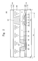
- FIG. 2 is a sectional view taken along line I-I' of FIG. 1.
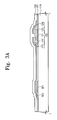
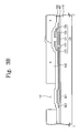
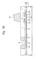
- FIG. 3A, FIG. 3B, FIG. 3C, FIG. 3D, and FIG. 3E are sectional views showing a method for manufacturing an array substrate and a spacer shown in FIG. 2.
- FIG. 4 is a plan view showing a liquid crystal display panel according to another exemplary embodiment of the present invention.
- FIG. 5 is a sectional view taken along line II-II' of FIG. 4.
- FIG. 6A, FIG. 6B, FIG. 6C, FIG. 6D, and FIG. 6E are sectional views showing a manufacturing process of an array substrate and a spacer shown in FIG. 5.
- FIG. 1 is a plan view showing a liquid crystal display panel according to an exemplary embodiment of the present invention
- FIG. 2 is a section view taken along line I-I' of FIG. 1.
- a liquid crystal display panel 500 includes an array substrate 100, an opposite substrate 200, and a liquid crystal layer 300.
- the array substrate 100 includes a first base substrate 110, a gate line GL, a data line DL, a thin film transistor 120, a pixel electrode 130, a color filter 140, and a black matrix 150.
- the first base substrate 110 is divided into a plurality of pixel areas that displays an image.
- the gate line GL extends in a first direction D1 on the first base substrate 110 to transmit a gate signal.
- the data line DL is insulated from and crosses the gate line GL to transmit a data signal.
- the data line DL and the gate line GL define a pixel area PA.
- the pixel area PA includes the thin film transistor 120, the pixel electrode 130, the color filter 140, and the black matrix 150.
- the thin film transistor 120 includes a gate electrode 121 branched from the gate line GL, an active layer 122, and an ohmic contact layer 123 sequentially formed on the gate electrode 121, a source electrode 124 branched from the data line DL and formed on the ohmic contact layer 123, and a drain electrode 125 formed from the same layer as the source electrode 124.
- the pixel electrode 130 is connected to the drain electrode 125 and outputs a pixel voltage.
- the pixel electrode 130 includes a transparent conductive material such as indium tin oxide (ITO) or indium zinc oxide (IZO).
- the array substrate 100 further includes a gate insulating layer 161 and a protective layer 162 to protect the metal wires.
- the gate insulating layer 161 is formed on the first base substrate 110 to cover the gate line GL and the gate electrode 121.
- the protective layer 162 is formed on the gate insulating layer 161 to cover the data line DL, the source electrode 124, and the drain electrode 125.
- the array substrate 100 further includes a common voltage line CL to transmit a common voltage, a first storage electrode SE1, and a second storage electrode SE2.
- the common voltage line CL is formed from the same layer as the gate line GL and extends in the first direction D1.
- the first storage electrode SE1 is branched from the common voltage line CL.
- the second storage line SE2 extends from the drain electrode 125 and is arranged on the first storage electrode SE1.
- the second storage line SE2 is connected to the pixel electrode 130.
- the gate insulating layer 161 is interposed between the first storage electrode SE1 and the second storage electrode SE2, and serves as a storage capacitor with the first storage electrode SE1 and the second storage electrode SE2.
- the color filter 140 is formed on the protective layer 162, and is arranged partially under the pixel electrode 130 and removed from a region corresponding to the second storage electrode SE2.
- the color filter 140 which displays a predetermined color using light, includes a red, green, or blue color filter and is formed in the pixel area PA. Also, the color filter 140 may be thick enough to planarize the array substrate 100. Thus, in this case, a separate organic insulating layer is not needed to planarize the array substrate 100.
- the black matrix 150 is arranged on the second storage electrode SE2 and under the pixel electrode 130.
- the color filter 140 surrounds the black matrix 150 in a plan view.
- the black matrix 150 includes a black organic material to block the light.
- the black matrix 150 and the protective layer 162 may be partially removed to form a contact hole CH, which exposes the second storage electrode SE2.
- the pixel electrode 130 is connected to the second storage electrode SE2 through the contact hole CH, so that the drain electrode 125 and the pixel electrode 130 are connected to each other. Since each contact hole CH is formed by removing the black matrix 150 in the corresponding pixel area PA, the contact holes CH in each pixel area PA may be the same size.
- the red, green, and blue color filters may have different material characteristics from each other.
- the color filters are etched using the same etching process, the etching amount of each color filter is different. Therefore, when the contact hole CH is formed by removing the color filter 140, the size of the contact hole CH may be different according to the color of the color filter 140.
- the black matrix 150 may be formed in each pixel area PA of the array substrate 100, and then a portion of the black matrix 150 may be removed to form the contact hole CH.
- the size of the contact hole CH in each pixel area PA may be the same, so that the pixel electrode 130 may not be insulated from the second storage electrode SE2, thereby improving product yield.
- the opposite substrate 200 is arranged on the array substrate 100.
- the opposite substrate 200 includes a second base substrate 210 coupled with the first base substrate 110 while facing the first base substrate 110 and a common electrode 220 formed on the second base substrate 210.
- the common electrode 220 includes a transparent conductive material such as ITO, IZO, etc., and provides the common voltage to the liquid crystal layer 300.
- the liquid crystal layer 300 controls the transmittance of light according to an electric field formed between the array substrate 100 and the opposite substrate 200.
- the liquid crystal display panel 500 further includes a spacer 400 that uniformly maintains a cell gap between the array substrate 100 and the opposite substrate 200.
- a spacer 400 is formed in each pixel area PA and arranged on the thin film transistor 120.
- the spacer 400 may include the same material as the black matrix 150 and may be formed through the same process as the black matrix 150. Since each spacer 400 and black matrix 150 may include the same material, the opposite substrate 200 may not require a separate black matrix to prevent the thin film transistor 120 from being recognized from the outside. As a result, the number of manufacturing processes may be decreased and misalignment between the array substrate 100 and the opposite substrate 200 may be prevented.
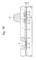
- FIG. 3A, FIG. 3B, FIG. 3C, FIG. 3D, and FIG. 3E are sectional views showing a method of manufacturing the array substrate and the spacer shown in FIG. 2.
- the gate insulating layer 161, the thin film transistor 120, the first storage electrode SE1, and the second storage electrode SE2 are formed on the first base substrate 110, and the protective layer 162 is formed on the first base substrate 110 to cover the gate insulating layer 161, the thin film transistor 120, the first storage electrode SE1, and the second storage electrode SE2.
- a photoresist layer (not shown) corresponding to the color filter 140 is coated over the protective layer 162 and is patterned to form the color filter 140. While patterning the photoresist layer, the photoresist layer is removed from an area corresponding to the second storage electrode SE2, to provide the color filter 140 with an opening 141.
- a black photoresist layer 10 including a black organic material is deposited on the first base substrate 110 and the opening 141 is filled with the black photoresist layer 10.
- the black photoresist layer 10 is patterned to form the black matrix 150 and the spacer 400. While patterning the black photoresist 10, the black matrix 150 is partially removed such that the protective layer 162 is exposed through the removed portion of the black matrix 150. Since the black matrix 150 and the spacer 400 are formed substantially simultaneously through the same process, it may be possible to reduce the number of masks, the number of manufacturing steps, and the manufacturing costs, thereby improving productivity.
- the protective layer 162 exposed through the removed portion of the black matrix 150 is removed to form the contact hole CH.
- the pixel electrode 130 is formed on the color filter 140 and the black matrix 150 such that the pixel electrode 130 contacts the second storage electrode SE2 through the contact hole CH, thereby completing the array substrate 100 and the spacer 400.
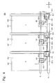
- FIG. 4 is a plan view showing a liquid crystal display panel according to another exemplary embodiment of the present invention
- FIG. 5 is a sectional view taken along line II-II' of FIG. 4.
- a liquid crystal display panel 900 includes an array substrate 600, a liquid crystal layer 300, and an opposite substrate 700.
- the liquid crystal layer 300 has same structure and function as that of the liquid crystal layer in FIG. 2, and thus, the same reference numeral is assigned to the liquid crystal layer and a detailed description of the liquid crystal layer will be omitted.
- the array substrate 600 includes a first base substrate 110, a gate line GL, a first data line DL1, a second data line DL2, a third data line DL3, a first thin film transistor 610, a second thin film transistor 620, a third thin film transistor 630, a first pixel electrode 641, a second pixel electrode 642, a third pixel electrode 643, a first color filter 651, a second color filter 652, and a third color filter 653.
- the first base substrate 110 includes a first pixel area PA1, a second pixel area PA2, and a third pixel area PA3 on which an image is displayed.
- the gate line GL formed on the first base substrate 110 extends in a first direction D1.
- the first, second, and third data lines DL1, DL2, and DL3 are insulated from and cross the gate line GL to define the first, second, and third pixel areas PA1, PA2, and PA3.
- the first, second, and third data lines DL1, DL2, and DL3 extend in the second direction D2.
- the first, second, and third thin film transistors 610, 620, and 630 are formed in the first, second, and third pixel areas PA1, PA2, and PA3, respectively, and are connected to the first, second, and third data lines DL1, DL2, and DL3, respectively.
- the first, second, and third thin film transistors 610, 620, and 630 each have the same configuration. Thus, only the first thin film transistor 610 will be described in detail and detailed descriptions of the second and third thin film transistors 620 and 630 will be omitted to avoid redundancy.
- the first thin film transistor 610 includes a gate electrode 611 branched from the gate line GL, an active layer 612, and an ohmic contact layer 613 sequentially formed on the gate electrode 611, a source electrode 614 branched from the data line DL1 and formed on the ohmic contact layer 613, and a drain electrode 615 formed from the same layer as the source electrode 614.
- the drain electrode 615 of the first thin film transistor 610, the drain electrode 625 of the second thin film transistor 620, and the drain electrode 635 of the third thin film transistor 630 are connected to the first pixel electrode 641, the second pixel electrode 642, and the third pixel electrode 643, respectively, to output a pixel voltage.
- the first, second, and third pixel electrodes 641, 642, and 643 are formed in the first, second, and third pixel areas PA1, PA2, and PA3, respectively, and each include a transparent conductive material such as ITO or IZO.
- the array substrate 600 further includes a gate insulating layer 161 and a protective layer 162 to protect the metal wires.
- the gate insulating layer 161 is arranged on the first base substrate 110 to cover the gate line GL and the gate electrodes.
- the protective layer 162 is arranged on the gate insulating layer 161 to cover the first, second, and third data lines DL1, DL2, and DL3 and the first, second, and third thin film transistors 610, 620, and 630.
- the array substrate 600 further includes a common voltage line CL, first storage electrodes SE1a, SE1b, and SE1c, and second storage electrodes SE2a, SE2b, and SE2c.
- the common voltage line CL is formed on the same layer as the gate line GL.
- the first storage electrodes SE1a, SE1b, and SE1c are branched from the common voltage line CL and arranged in the first, second, and third pixel areas PA1, PA2, and PA3, respectively.
- the second storage electrodes SE2a, SE2b, and SE2c extend from the drain electrodes 615, 625, and 635 of the first, second, and third thin film transistors 610, 620, and 630, respectively, and are arranged on the first storage electrodes SE1a, SE1b, and SE1c, respectively.
- the first color filter 651, the second color filter 652, and the third color filter 653 are formed on the protective layer 162.
- Each color filter 651, 652, and 653 includes a different color and displays the color using light.
- each color filter 651, 652, and 653 includes a red, green, or blue color filter.
- the first color filter 651 is formed in the first pixel area PA1 and is partially removed in the area corresponding to the second storage electrode SE2a of the first pixel area PA1.
- the second color filter 652 is formed in the second pixel area PA2 and is partially removed in the area corresponding to the second storage electrode SE2b of the second pixel area PA2.
- the first pixel electrode 641 and the second pixel electrode 642 are formed on the first color filter 651 and the second color filter 652, respectively.
- the third color filter 653 covers the entire third pixel area PA3 and is arranged on the storage electrode SE2a of the first pixel area PA1 and the storage electrode SE2b of the second pixel area PA2.
- the third color filter 653 is arranged partially under the first and second pixel electrodes 641 and 642 in the first and the second pixel areas PA1 and PA2, respectively, and is arranged under the third pixel electrode 643 in the third pixel area PA3.
- the first and second color filters 651 and 652 surround the third color filter 653 in the first and the second pixel areas PA1 and PA2, respectively, in a plan view.
- the third color filter 653 and the protective layer 162 are partially removed to form contact holes CH1, CH2, and CH3.
- the contact holes CH1, CH2, and CH3 are formed in the first, second, and third pixel areas PA1, PA2, and PA3, respectively, and the second storage electrodes SE2a, SE2b, and SE2c are exposed through the contact holes CH1, CH2, and CH3, respectively.
- the first, second, and third pixel electrodes 641, 642, and 643 are connected to the second storage electrodes SE2a, SE2b, and SE2c through the contact holes CH1, CH2, and CH3, respectively, thereby connecting the first, second, and third pixel electrodes 641, 642, and 643 and the first, second, and third thin film transistors 610, 620, and 630, respectively.
- the third color filter 653 is formed in each of the first, second, and third pixel areas PA1, PA2, and PA3 and is partially removed to form the contact holes CH1, CH2, and CH3.
- the contact holes CH1, CH2, and CH3 are the same size to prevent the first, second, and third pixel electrodes 641, 642, and 643 from being insulated from the second storage electrodes SE2a, SE2b, and SE2c, thereby improving product yield.
- the opposite substrate 700 is arranged on the array substrate 600.
- the opposite substrate 700 includes a second base substrate 210 facing the first base substrate 110, a black matrix 710 arranged on the second base substrate 210, an overcoat layer 720 arranged on the second base substrate 210 to cover the black matrix 710, and a common electrode 730 formed on the overcoat layer 720.
- the black matrix 710 is arranged corresponding to the first, second, and third thin film transistors 610, 620, and 630 and blocks the light.
- the black matrix 710 may include an organic material or a metallic material to block the light.
- the liquid crystal display panel 900 further includes spacers 810, 820, and 830 to maintain a cell gap between the array substrate 600 and the opposite substrate 700.
- the spacers 810, 820, and 830 are interposed between the array substrate 600 and the opposite substrate 700 and include the same material as the third color filter 653.
- the spacers 810, 820, and 830 are formed through the same process as the third color filter 653 and thus, are formed substantially simultaneously with the third color filter 653.
- the number of masks, the number of manufacturing steps, and the manufacturing costs may be reduced, thereby improving productivity.
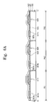
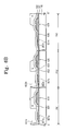
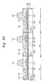
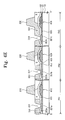
- FIG. 6A, FIG. 6B, FIG. 6C, FIG. 6D, and FIG. 6E are sectional views showing a method of manufacturing the array substrate and the spacer shown in FIG. 5.
- the first, second, and third thin film transistors 610, 620, and 630, the gate insulating layer 161, and the first and second storage electrodes SE1a, SE1b, SE1c, SE2a, SE2b, and SE2c are formed on the first base substrate 110.
- the protective layer 162 is also formed on the first base substrate 110 to cover the first, second, and third thin film transistors 610, 620, and 630, the gate insulating layer 161, and the first and second storage electrodes SE1a, SE1b, SE1c, SE2a, SE2b, and SE2c.
- a first photoresist layer (not shown) is deposited on the protective layer 162 and patterned to form the first color filter 651 in the first pixel area PA1. While patterning the first photoresist layer, the first color filter 651 is partially removed in the area corresponding to the second storage electrode SE2a of the first pixel area PA1 to form an opening 651a.
- a second photoresist layer (not shown) is deposited on the protective layer 162 and patterned to form the second color filter 652 in the second pixel area PA2. While patterning the second photoresist layer, the second color filter 652 is partially removed in the area corresponding to the second storage electrode SE2b of the second pixel area PA2 to form an opening 652a.
- a third photoresist layer 20 is deposited on the protective layer 162.
- the third photoresist layer 20 is patterned to form the third color filter 653 and the spacers 810, 820, and 830. While patterning the third photoresist layer 20, the third color filter 653 is partially removed on the second storage electrodes SE2a, SE2b, and SE2c to form the contact holes CH1, CH2, and CH3. Since the third color filter 653 and the spacers 810, 820, and 830 are formed substantially simultaneously through the same process, it may be possible to reduce the number of masks, the number of manufacturing steps, and the manufacturing costs, thereby improving productivity.
- the protective layer 162 is partially removed to form the contact holes CH1, CH2, and CH3. Then, the first, second, and third pixel electrodes 641, 642, and 643 are formed, completing the array substrate 600 and the spacers 810, 820, and 830.
- the array substrate may include color filters having two or more colors, and the black matrix may be partially removed to form a contact hole in each pixel area.
- the contact holes have the same size, and the pixel electrode is connected to the thin film transistor, which may improve product yield.
- the black matrix and the spacer of the liquid crystal display panel are formed substantially simultaneously through the same process using the same material, so that the number of masks, the number of manufacturing steps, and the manufacturing costs may be reduced, thereby improving productivity.
- the array substrate may include color filters that display an image and the color filters may be formed in corresponding pixel areas. Each color filter is partially removed to form a contact hole in each pixel area. Thus, it may be possible to prevent the pixel electrode from being insulated from the thin film transistor, thereby improving product yield.
- the color filter, through which the contact hole is formed, and the spacer of the liquid crystal display panel are formed substantially simultaneously through the same process using the same material, it may be possible to reduce the number of masks, the number of manufacturing steps, and the manufacturing costs, thereby improving productivity. It will be apparent to those skilled in the art that various modifications and variations can be made in the present invention without departing from the spirit or scope of the invention. Thus, it is intended that the present invention cover the modifications and variations of this invention provided they come within the scope of the appended claims and their equivalents.
Landscapes
- Physics & Mathematics (AREA)
- Nonlinear Science (AREA)
- Mathematical Physics (AREA)
- Chemical & Material Sciences (AREA)
- Crystallography & Structural Chemistry (AREA)
- General Physics & Mathematics (AREA)
- Optics & Photonics (AREA)
- Engineering & Computer Science (AREA)
- Microelectronics & Electronic Packaging (AREA)
- Liquid Crystal (AREA)
- Devices For Indicating Variable Information By Combining Individual Elements (AREA)
Abstract
Description
- This application claims priority from and the benefit of
Korean Patent Application No. 10-2006-0091388, filed on September 20, 2006 - The present invention relates to an array substrate, a display panel including the array substrate, and a method of manufacturing the array substrate. More particularly, the present invention relates to an array substrate having a color filter-on-array (COA) structure, a display apparatus including the array substrate, and a method of manufacturing the array substrate.
- In general, a COA-type liquid crystal display panel includes an array substrate, an opposite substrate facing the array substrate, and a liquid crystal layer interposed between the array substrate and the opposite substrate.
- The array substrate includes a plurality of pixels that displays an image. Each pixel includes a gate line, a data line, a thin film transistor, a pixel electrode, and a color filter. The gate line and the data line receive a gate signal and a data signal, respectively, and are connected to a gate electrode and a source electrode of the thin film transistor, respectively. The pixel electrode is connected to a drain electrode of the thin film transistor and outputs a pixel voltage. The color filter is arranged under the pixel electrode and displays a predetermined color using a light. The pixel electrode is connected to the drain electrode of the thin film transistor through a contact hole formed in the color filter.
- The color filter may be a red filter, a green filter, or a blue filter. Since the material characteristics of the red, green, and blue filters are different from each other, the exposure amount required for a contact hole to be formed through each differs, even though the contact holes are formed under the same process conditions. Thus, the sizes of the contact holes are different in the red, green, and blue filters, and if the size of a contact hole becomes too small, the drain electrode of the thin film transistor may not be exposed. As a result, the thin film transistor and the pixel electrode may be insulated from each other and an abnormal image may be displayed.
- The present invention provides an array substrate that may be capable of improving product yield.
- The present invention also provides a display panel including the above array substrate.
- The present invention also provides a method for manufacturing the above display panel.
- Additional features of the invention will be set forth in the description which follows, and in part will be apparent from the description, or may be learned by practice of the invention.
- The present invention discloses an array substrate including a base substrate, thin film transistors, pixel electrodes, insulation members, and a color filter layer. The base substrate includes a plurality of pixel area to display an image and a thin film transistor is arranged in each pixel area. A pixel electrode is arranged in each pixel area and is connected to the thin film transistor. An insulation member is arranged in each pixel area and provided with a contact hole through which the thin film transistor is exposed. The insulation members all include the same material. The color filter layer includes color filters arranged under the pixel electrode to surround the insulation members.
- The present invention also discloses a liquid crystal display panel including an array substrate and an opposite substrate facing the array substrate. The array substrate includes a first base substrate, thin film transistors, pixel electrodes, insulation members, and a color filter layer. The first base substrate includes a plurality of pixel areas to display an image. The thin film transistor is arranged in each pixel areas. The pixel electrode is arranged in each pixel area and is connected to the thin film transistor. The insulation members all include the same material. An insulation member is arranged in each pixel area and is provided with a contact hole through which the thin film transistor is exposed. The color filter layer includes color filters arranged under the pixel electrode to surround the insulation members.
- The present invention also discloses a method for manufacturing a display panel including forming a thin film transistor, a first storage electrode, and a second storage electrode in a pixel area of a first base substrate. The second storage electrode is branched from a drain electrode of the thin film transistor and disposed on the first storage electrode. A color filter is formed in the pixel area. A color filter formed on the second storage electrode is removed. A black matrix that including a contact hole is formed on the second storage electrode. A pixel electrode is formed on the color filter and the black matrix such that the pixel electrode is connected to the second storage electrode through the contact hole. A common electrode is formed on a second base substrate. The first base substrate is coupled with the second base substrate.
- It is to be understood that both the foregoing general description and the following detailed description are exemplary and explanatory and are intended to provide a further explanation of the invention as claimed.
- The accompanying drawings, which are included to provide a further understanding of the invention and are incorporated in and constitute a part of this specification, illustrate embodiments of the invention, and together with the description serve to explain the principles of the invention.
- FIG. 1 is a plan view showing a liquid crystal display panel according to an exemplary embodiment of the present invention
- FIG. 2 is a sectional view taken along line I-I' of FIG. 1.
- FIG. 3A, FIG. 3B, FIG. 3C, FIG. 3D, and FIG. 3E are sectional views showing a method for manufacturing an array substrate and a spacer shown in FIG. 2.
- FIG. 4 is a plan view showing a liquid crystal display panel according to another exemplary embodiment of the present invention;
- FIG. 5 is a sectional view taken along line II-II' of FIG. 4.
- FIG. 6A, FIG. 6B, FIG. 6C, FIG. 6D, and FIG. 6E are sectional views showing a manufacturing process of an array substrate and a spacer shown in FIG. 5.
- The invention is described more fully hereinafter with reference to the accompanying drawings, in which embodiments of the invention are shown. This invention may, however, be embodied in many different forms and should not be construed as limited to the embodiments set forth herein. Rather, these embodiments are provided so that this disclosure is thorough, and will fully convey the scope of the invention to those skilled in the art. In the drawings, the size and relative sizes of layers and regions may be exaggerated for clarity. Like reference numerals in the drawings denote like elements.
- It will be understood that when an element or layer is referred to as being "on" or "connected to" another element or layer, it can be directly on or directly connected to the other element or layer, or intervening elements or layer may be present. In contrast, when an element is referred to as being "directly on" or "directly connected to" another element or layer, there are no intervening elements or layers present.
- FIG. 1 is a plan view showing a liquid crystal display panel according to an exemplary embodiment of the present invention, and FIG. 2 is a section view taken along line I-I' of FIG. 1.
- Referring to FIG. 1 and FIG. 2, a liquid
crystal display panel 500 includes anarray substrate 100, anopposite substrate 200, and aliquid crystal layer 300. - The
array substrate 100 includes afirst base substrate 110, a gate line GL, a data line DL, athin film transistor 120, apixel electrode 130, acolor filter 140, and ablack matrix 150. - The
first base substrate 110 is divided into a plurality of pixel areas that displays an image. - The gate line GL extends in a first direction D1 on the
first base substrate 110 to transmit a gate signal. - The data line DL is insulated from and crosses the gate line GL to transmit a data signal. The data line DL and the gate line GL define a pixel area PA.
- The pixel area PA includes the
thin film transistor 120, thepixel electrode 130, thecolor filter 140, and theblack matrix 150. Thethin film transistor 120 includes agate electrode 121 branched from the gate line GL, anactive layer 122, and anohmic contact layer 123 sequentially formed on thegate electrode 121, asource electrode 124 branched from the data line DL and formed on theohmic contact layer 123, and adrain electrode 125 formed from the same layer as thesource electrode 124. - The
pixel electrode 130 is connected to thedrain electrode 125 and outputs a pixel voltage. Thepixel electrode 130 includes a transparent conductive material such as indium tin oxide (ITO) or indium zinc oxide (IZO). - The
array substrate 100 further includes agate insulating layer 161 and aprotective layer 162 to protect the metal wires. Thegate insulating layer 161 is formed on thefirst base substrate 110 to cover the gate line GL and thegate electrode 121. Theprotective layer 162 is formed on thegate insulating layer 161 to cover the data line DL, thesource electrode 124, and thedrain electrode 125. - Also, the
array substrate 100 further includes a common voltage line CL to transmit a common voltage, a first storage electrode SE1, and a second storage electrode SE2. The common voltage line CL is formed from the same layer as the gate line GL and extends in the first direction D1. The first storage electrode SE1 is branched from the common voltage line CL. The second storage line SE2 extends from thedrain electrode 125 and is arranged on the first storage electrode SE1. The second storage line SE2 is connected to thepixel electrode 130. Thegate insulating layer 161 is interposed between the first storage electrode SE1 and the second storage electrode SE2, and serves as a storage capacitor with the first storage electrode SE1 and the second storage electrode SE2. - The
color filter 140 is formed on theprotective layer 162, and is arranged partially under thepixel electrode 130 and removed from a region corresponding to the second storage electrode SE2. Thecolor filter 140, which displays a predetermined color using light, includes a red, green, or blue color filter and is formed in the pixel area PA. Also, thecolor filter 140 may be thick enough to planarize thearray substrate 100. Thus, in this case, a separate organic insulating layer is not needed to planarize thearray substrate 100. - The
black matrix 150 is arranged on the second storage electrode SE2 and under thepixel electrode 130. Thecolor filter 140 surrounds theblack matrix 150 in a plan view. Theblack matrix 150 includes a black organic material to block the light. Theblack matrix 150 and theprotective layer 162 may be partially removed to form a contact hole CH, which exposes the second storage electrode SE2. Thepixel electrode 130 is connected to the second storage electrode SE2 through the contact hole CH, so that thedrain electrode 125 and thepixel electrode 130 are connected to each other. Since each contact hole CH is formed by removing theblack matrix 150 in the corresponding pixel area PA, the contact holes CH in each pixel area PA may be the same size. - In general, the red, green, and blue color filters may have different material characteristics from each other. Thus, although the color filters are etched using the same etching process, the etching amount of each color filter is different. Therefore, when the contact hole CH is formed by removing the
color filter 140, the size of the contact hole CH may be different according to the color of thecolor filter 140. - In order to prevent the above-described disadvantage, the
black matrix 150 may be formed in each pixel area PA of thearray substrate 100, and then a portion of theblack matrix 150 may be removed to form the contact hole CH. Thus, the size of the contact hole CH in each pixel area PA may be the same, so that thepixel electrode 130 may not be insulated from the second storage electrode SE2, thereby improving product yield. - The
opposite substrate 200 is arranged on thearray substrate 100. Theopposite substrate 200 includes asecond base substrate 210 coupled with thefirst base substrate 110 while facing thefirst base substrate 110 and acommon electrode 220 formed on thesecond base substrate 210. Thecommon electrode 220 includes a transparent conductive material such as ITO, IZO, etc., and provides the common voltage to theliquid crystal layer 300. Theliquid crystal layer 300 controls the transmittance of light according to an electric field formed between thearray substrate 100 and theopposite substrate 200. - The liquid
crystal display panel 500 further includes aspacer 400 that uniformly maintains a cell gap between thearray substrate 100 and theopposite substrate 200. Aspacer 400 is formed in each pixel area PA and arranged on thethin film transistor 120. Thespacer 400 may include the same material as theblack matrix 150 and may be formed through the same process as theblack matrix 150. Since eachspacer 400 andblack matrix 150 may include the same material, theopposite substrate 200 may not require a separate black matrix to prevent thethin film transistor 120 from being recognized from the outside. As a result, the number of manufacturing processes may be decreased and misalignment between thearray substrate 100 and theopposite substrate 200 may be prevented. - FIG. 3A, FIG. 3B, FIG. 3C, FIG. 3D, and FIG. 3E are sectional views showing a method of manufacturing the array substrate and the spacer shown in FIG. 2.
- Referring to FIG. 3A, the
gate insulating layer 161, thethin film transistor 120, the first storage electrode SE1, and the second storage electrode SE2 are formed on thefirst base substrate 110, and theprotective layer 162 is formed on thefirst base substrate 110 to cover thegate insulating layer 161, thethin film transistor 120, the first storage electrode SE1, and the second storage electrode SE2. - Referring to FIG. 3B, a photoresist layer (not shown) corresponding to the
color filter 140 is coated over theprotective layer 162 and is patterned to form thecolor filter 140. While patterning the photoresist layer, the photoresist layer is removed from an area corresponding to the second storage electrode SE2, to provide thecolor filter 140 with anopening 141. - Referring to FIG. 3C and FIG. 3D, a
black photoresist layer 10 including a black organic material is deposited on thefirst base substrate 110 and theopening 141 is filled with theblack photoresist layer 10. - Then, the
black photoresist layer 10 is patterned to form theblack matrix 150 and thespacer 400. While patterning theblack photoresist 10, theblack matrix 150 is partially removed such that theprotective layer 162 is exposed through the removed portion of theblack matrix 150. Since theblack matrix 150 and thespacer 400 are formed substantially simultaneously through the same process, it may be possible to reduce the number of masks, the number of manufacturing steps, and the manufacturing costs, thereby improving productivity. - Referring to FIG. 2 and FIG. 3E, the
protective layer 162 exposed through the removed portion of theblack matrix 150 is removed to form the contact hole CH. Then, thepixel electrode 130 is formed on thecolor filter 140 and theblack matrix 150 such that thepixel electrode 130 contacts the second storage electrode SE2 through the contact hole CH, thereby completing thearray substrate 100 and thespacer 400. - FIG. 4 is a plan view showing a liquid crystal display panel according to another exemplary embodiment of the present invention, and FIG. 5 is a sectional view taken along line II-II' of FIG. 4.
- Referring to FIG. 4 and FIG. 5, a liquid
crystal display panel 900 includes anarray substrate 600, aliquid crystal layer 300, and anopposite substrate 700. In the present exemplary embodiment, theliquid crystal layer 300 has same structure and function as that of the liquid crystal layer in FIG. 2, and thus, the same reference numeral is assigned to the liquid crystal layer and a detailed description of the liquid crystal layer will be omitted. - The
array substrate 600 includes afirst base substrate 110, a gate line GL, a first data line DL1, a second data line DL2, a third data line DL3, a firstthin film transistor 610, a secondthin film transistor 620, a thirdthin film transistor 630, afirst pixel electrode 641, asecond pixel electrode 642, athird pixel electrode 643, afirst color filter 651, asecond color filter 652, and athird color filter 653. - The
first base substrate 110 includes a first pixel area PA1, a second pixel area PA2, and a third pixel area PA3 on which an image is displayed. The gate line GL formed on thefirst base substrate 110 extends in a first direction D1. The first, second, and third data lines DL1, DL2, and DL3 are insulated from and cross the gate line GL to define the first, second, and third pixel areas PA1, PA2, and PA3. The first, second, and third data lines DL1, DL2, and DL3 extend in the second direction D2. - The first, second, and third
thin film transistors thin film transistors thin film transistor 610 will be described in detail and detailed descriptions of the second and thirdthin film transistors - The first
thin film transistor 610 includes agate electrode 611 branched from the gate line GL, anactive layer 612, and anohmic contact layer 613 sequentially formed on thegate electrode 611, asource electrode 614 branched from the data line DL1 and formed on theohmic contact layer 613, and adrain electrode 615 formed from the same layer as thesource electrode 614. - The
drain electrode 615 of the firstthin film transistor 610, thedrain electrode 625 of the secondthin film transistor 620, and thedrain electrode 635 of the thirdthin film transistor 630 are connected to thefirst pixel electrode 641, thesecond pixel electrode 642, and thethird pixel electrode 643, respectively, to output a pixel voltage. The first, second, andthird pixel electrodes - The
array substrate 600 further includes agate insulating layer 161 and aprotective layer 162 to protect the metal wires. Thegate insulating layer 161 is arranged on thefirst base substrate 110 to cover the gate line GL and the gate electrodes. Theprotective layer 162 is arranged on thegate insulating layer 161 to cover the first, second, and third data lines DL1, DL2, and DL3 and the first, second, and thirdthin film transistors - Also, the
array substrate 600 further includes a common voltage line CL, first storage electrodes SE1a, SE1b, and SE1c, and second storage electrodes SE2a, SE2b, and SE2c. The common voltage line CL is formed on the same layer as the gate line GL. The first storage electrodes SE1a, SE1b, and SE1c are branched from the common voltage line CL and arranged in the first, second, and third pixel areas PA1, PA2, and PA3, respectively. The second storage electrodes SE2a, SE2b, and SE2c extend from thedrain electrodes thin film transistors - The
first color filter 651, thesecond color filter 652, and thethird color filter 653 are formed on theprotective layer 162. Eachcolor filter color filter - The
first color filter 651 is formed in the first pixel area PA1 and is partially removed in the area corresponding to the second storage electrode SE2a of the first pixel area PA1. Thesecond color filter 652 is formed in the second pixel area PA2 and is partially removed in the area corresponding to the second storage electrode SE2b of the second pixel area PA2. Thefirst pixel electrode 641 and thesecond pixel electrode 642 are formed on thefirst color filter 651 and thesecond color filter 652, respectively. - The
third color filter 653 covers the entire third pixel area PA3 and is arranged on the storage electrode SE2a of the first pixel area PA1 and the storage electrode SE2b of the second pixel area PA2. Thethird color filter 653 is arranged partially under the first andsecond pixel electrodes third pixel electrode 643 in the third pixel area PA3. The first andsecond color filters third color filter 653 in the first and the second pixel areas PA1 and PA2, respectively, in a plan view. - The
third color filter 653 and theprotective layer 162 are partially removed to form contact holes CH1, CH2, and CH3. The contact holes CH1, CH2, and CH3 are formed in the first, second, and third pixel areas PA1, PA2, and PA3, respectively, and the second storage electrodes SE2a, SE2b, and SE2c are exposed through the contact holes CH1, CH2, and CH3, respectively. The first, second, andthird pixel electrodes third pixel electrodes thin film transistors - As described above, the
third color filter 653 is formed in each of the first, second, and third pixel areas PA1, PA2, and PA3 and is partially removed to form the contact holes CH1, CH2, and CH3. Thus, the contact holes CH1, CH2, and CH3 are the same size to prevent the first, second, andthird pixel electrodes - The
opposite substrate 700 is arranged on thearray substrate 600. Theopposite substrate 700 includes asecond base substrate 210 facing thefirst base substrate 110, ablack matrix 710 arranged on thesecond base substrate 210, anovercoat layer 720 arranged on thesecond base substrate 210 to cover theblack matrix 710, and acommon electrode 730 formed on theovercoat layer 720. - The
black matrix 710 is arranged corresponding to the first, second, and thirdthin film transistors black matrix 710 may include an organic material or a metallic material to block the light. - The liquid
crystal display panel 900 further includesspacers array substrate 600 and theopposite substrate 700. Thespacers array substrate 600 and theopposite substrate 700 and include the same material as thethird color filter 653. Thespacers third color filter 653 and thus, are formed substantially simultaneously with thethird color filter 653. Thus, the number of masks, the number of manufacturing steps, and the manufacturing costs may be reduced, thereby improving productivity. - FIG. 6A, FIG. 6B, FIG. 6C, FIG. 6D, and FIG. 6E are sectional views showing a method of manufacturing the array substrate and the spacer shown in FIG. 5.
- Referring to FIG. 6A, the first, second, and third
thin film transistors gate insulating layer 161, and the first and second storage electrodes SE1a, SE1b, SE1c, SE2a, SE2b, and SE2c are formed on thefirst base substrate 110. Theprotective layer 162 is also formed on thefirst base substrate 110 to cover the first, second, and thirdthin film transistors gate insulating layer 161, and the first and second storage electrodes SE1a, SE1b, SE1c, SE2a, SE2b, and SE2c. - Referring to FIG. 6B, a first photoresist layer (not shown) is deposited on the
protective layer 162 and patterned to form thefirst color filter 651 in the first pixel area PA1. While patterning the first photoresist layer, thefirst color filter 651 is partially removed in the area corresponding to the second storage electrode SE2a of the first pixel area PA1 to form anopening 651a. - Then, a second photoresist layer (not shown) is deposited on the
protective layer 162 and patterned to form thesecond color filter 652 in the second pixel area PA2. While patterning the second photoresist layer, thesecond color filter 652 is partially removed in the area corresponding to the second storage electrode SE2b of the second pixel area PA2 to form anopening 652a. - Referring to FIG. 6C and FIG. 6D, a
third photoresist layer 20 is deposited on theprotective layer 162. Theopenings first color filter 651 and thesecond color filter 652, respectively, are filled with thethird photoresist layer 20. - Then, the
third photoresist layer 20 is patterned to form thethird color filter 653 and thespacers third photoresist layer 20, thethird color filter 653 is partially removed on the second storage electrodes SE2a, SE2b, and SE2c to form the contact holes CH1, CH2, and CH3. Since thethird color filter 653 and thespacers - Referring to FIG. 5 and FIG. 6E, the
protective layer 162 is partially removed to form the contact holes CH1, CH2, and CH3. Then, the first, second, andthird pixel electrodes array substrate 600 and thespacers - According to the above, the array substrate may include color filters having two or more colors, and the black matrix may be partially removed to form a contact hole in each pixel area. Thus, the contact holes have the same size, and the pixel electrode is connected to the thin film transistor, which may improve product yield.
- Also, the black matrix and the spacer of the liquid crystal display panel are formed substantially simultaneously through the same process using the same material, so that the number of masks, the number of manufacturing steps, and the manufacturing costs may be reduced, thereby improving productivity.
- The array substrate may include color filters that display an image and the color filters may be formed in corresponding pixel areas. Each color filter is partially removed to form a contact hole in each pixel area. Thus, it may be possible to prevent the pixel electrode from being insulated from the thin film transistor, thereby improving product yield.
- Also, since the color filter, through which the contact hole is formed, and the spacer of the liquid crystal display panel are formed substantially simultaneously through the same process using the same material, it may be possible to reduce the number of masks, the number of manufacturing steps, and the manufacturing costs, thereby improving productivity.
It will be apparent to those skilled in the art that various modifications and variations can be made in the present invention without departing from the spirit or scope of the invention. Thus, it is intended that the present invention cover the modifications and variations of this invention provided they come within the scope of the appended claims and their equivalents.
Claims (20)
- An array substrate, comprising:a base substrate on which a plurality of pixel areas is defined to display an image;a thin film transistor arranged in each pixel area;an insulation member arranged in each pixel area and provided with a contact hole through which the thin film transistor is exposed, the insulation members all comprising the same material;a pixel electrode arranged in each pixel area to cover the insulation member, the pixel electrode being connected to the thin film transistor through the contact hole; anda color filter layer comprising color filters arranged under the pixel electrode to surround the insulation members.
- The array substrate of claim 1, wherein the insulation member comprises an organic material to block light.
- The array substrate of claim 1, wherein the insulation member comprises of the same material as a color filter.
- The array substrate of claim 3, wherein the color filters of the color filter layer comprise red, green, and blue filters, a color filter is arranged in each pixel area, and the insulation member comprises of the same material as either the red, green, or blue color filter.
- The array substrate of claim 1, further comprising:a first storage electrode arranged in each pixel area; anda second storage electrode arranged on and insulated from the first storage electrode.
- The array substrate of claim 5, wherein the insulation member is positioned on the second storage electrode, and the pixel electrode is connected to the thin film transistor via second storage electrode.
- The array substrate of claim 6, wherein the second storage electrode extends from a drain electrode of the thin film transistor.
- The array substrate of claim 7, further comprising:a gate line arranged on the base substrate to transmit a gate signal;a data line insulated from and crossing the gate line to define a pixel area and transmit a data signal corresponding to the image; anda common voltage line extending in a same direction as the gate line to transmit a common voltage,wherein the first storage electrode is branched from the common voltage line.
- A display panel comprising:an array substrate; andan opposite substrate facing the array substrate,the array substrate comprising:a first base substrate on which a plurality of pixel areas is defined to display an image;a thin film transistor arranged in each pixel area;an insulation member arranged in each pixel area and provided with a contact hole through which the thin film transistor is exposed, the insulation members all comprising the same material;a pixel electrode arranged in each pixel area to cover the insulation member, the pixel electrode being connected to the thin film transistor through the contact hole; anda color filter layer comprising color filters arranged under the pixel electrode to surround the insulation members.
- The display panel of claim 9, further comprising a spacer interposed between the array substrate and the opposite substrate to maintain a cell gap between the array substrate and the opposite substrate, the spacer comprising the same material as the insulation member.
- The display panel of claim 10, wherein the spacer is positioned on an upper portion of the thin film transistor.
- The display panel of claim 10, wherein the opposite substrate comprises:a second base substrate facing the first base substrate; anda common electrode arranged on the second base substrate.
- The display panel of claim 12, wherein the insulation member comprises an organic material to block light.
- The display panel of claim 12, wherein the color filters of the color filter layer comprise red, green, and blue filters, a color filter is arranged in each pixel area, and the insulation member comprises the same material as either the red, green, or blue color filter.
- The display panel of claim 14, wherein the opposite substrate further comprises a black matrix arranged on the second base substrate and between the pixel areas to block light.
- The display panel of claim 9, further comprising a liquid crystal layer disposed between the array substrate and the opposite substrate to adjust a transmittance of a light applied thereto.
- A method of manufacturing a display panel, comprising:forming a thin film transistor, a first storage electrode, and a second storage electrode in a pixel area of a first base substrate, the second storage electrode being branched from a drain electrode of the thin film transistor and disposed on the first storage electrode;forming a color filter in the pixel area;removing the color filter formed on the second storage electrode;forming a black matrix on the second storage electrode, the black matrix being provided with a contact hole;forming a pixel electrode on the color filter and the black matrix such that the pixel electrode is connected to the second storage electrode through the contact hole;forming a common electrode on a second base substrate; andcoupling the first base substrate with the second base substrate.
- The method of claim 17, wherein forming a black matrix comprises:forming a black photoresist layer on the first base substrate; andpatterning the black photoresist layer to form the black matrix and the contact hole.
- The method of claim 18, further comprising forming a spacer on the thin film transistor to maintain a cell gap between the first base substrate and the second base substrate, the spacer being formed before the pixel electrode.
- The method of claim 19, wherein the spacer is formed substantially simultaneously with the black matrix.
Applications Claiming Priority (1)
| Application Number | Priority Date | Filing Date | Title |
|---|---|---|---|
| KR1020060091388A KR101335276B1 (en) | 2006-09-20 | 2006-09-20 | Array substrat, display panel having the same and fabricating of display panel |
Publications (3)
| Publication Number | Publication Date |
|---|---|
| EP1909133A2 true EP1909133A2 (en) | 2008-04-09 |
| EP1909133A3 EP1909133A3 (en) | 2009-03-11 |
| EP1909133B1 EP1909133B1 (en) | 2013-01-23 |
Family
ID=39102921
Family Applications (1)
| Application Number | Title | Priority Date | Filing Date |
|---|---|---|---|
| EP07018164A Active EP1909133B1 (en) | 2006-09-20 | 2007-09-15 | Array substrate, display panel having the same and method of manufacturing the same |
Country Status (3)
| Country | Link |
|---|---|
| US (2) | US7817227B2 (en) |
| EP (1) | EP1909133B1 (en) |
| KR (1) | KR101335276B1 (en) |
Families Citing this family (40)
| Publication number | Priority date | Publication date | Assignee | Title |
|---|---|---|---|---|
| TWI381230B (en) * | 2008-01-31 | 2013-01-01 | Hannstar Display Corp | Pixel structure of liquid crystal display |
| KR101499226B1 (en) * | 2008-07-25 | 2015-03-05 | 삼성디스플레이 주식회사 | Thin film transistor display panel and manufacturing method thereof |
| KR101557817B1 (en) * | 2008-12-15 | 2015-10-07 | 삼성디스플레이 주식회사 | Thin film transistor display panel and manufacturing method thereof |
| TWI391735B (en) * | 2009-07-06 | 2013-04-01 | Au Optronics Corp | Color filter array on pixel array substrate and display panel |
| US20120194772A1 (en) * | 2009-10-08 | 2012-08-02 | Sharp Kabushiki Kaisha | Liquid crystal display device and method for manufacturing same |
| KR101620531B1 (en) * | 2009-10-08 | 2016-05-13 | 삼성디스플레이 주식회사 | Liquid crystal display |
| TWI395016B (en) * | 2009-10-14 | 2013-05-01 | Au Optronics Corp | Active device array substrate and manufacturing method thereof |
| KR101604650B1 (en) | 2009-10-27 | 2016-03-28 | 삼성디스플레이 주식회사 | Display substrate, method for manufacturing the same and method for manufacturing display panel |
| KR101682092B1 (en) | 2009-11-12 | 2016-12-05 | 삼성디스플레이 주식회사 | Thin film transistor array panel and liquid crystal display including the same |
| KR101620534B1 (en) | 2010-01-29 | 2016-05-13 | 삼성디스플레이 주식회사 | Liquid crystal display |
| KR101761180B1 (en) * | 2010-08-10 | 2017-07-26 | 삼성디스플레이 주식회사 | Display substrate, display device comprising the same and method of manufacturing the same |
| KR20130100200A (en) | 2010-12-14 | 2013-09-09 | 캐보트 코포레이션 | Methods to control electrical resistivity in filler-polymer compositions and products related thereto |
| CN102929058B (en) * | 2012-11-12 | 2015-07-08 | 京东方科技集团股份有限公司 | Array substrate, manufacturing method of array substrate, and display device |
| CN104035231B (en) * | 2013-03-07 | 2017-04-12 | 群创光电股份有限公司 | Liquid crystal display panel and liquid crystal display device comprising same |
| TWI516836B (en) | 2013-03-07 | 2016-01-11 | 群創光電股份有限公司 | Liquid crystal display panel and liquid crystal display device containing the same |
| CN105209558A (en) | 2013-03-13 | 2015-12-30 | 卡博特公司 | Coatings having filler-polymer compositions having combined low dielectric constant, high resistivity, and optical density properties and controlled resistivity, devices made therefrom, and methods of making same |
| KR20140147299A (en) * | 2013-06-19 | 2014-12-30 | 삼성디스플레이 주식회사 | Curved display device and manufacturing method thereof |
| KR102122402B1 (en) * | 2013-12-31 | 2020-06-15 | 엘지디스플레이 주식회사 | COT Structure Liquid Crystal Display Device and method of fabricating the same |
| KR102166898B1 (en) | 2014-01-10 | 2020-10-19 | 삼성디스플레이 주식회사 | Thin film transistor array panel and method for manufacturing the same |
| KR102360783B1 (en) | 2014-09-16 | 2022-02-10 | 삼성디스플레이 주식회사 | display device |
| CN104298040B (en) * | 2014-10-31 | 2018-07-06 | 京东方科技集团股份有限公司 | A kind of COA substrates and preparation method thereof and display device |
| KR102179555B1 (en) * | 2014-10-31 | 2020-11-18 | 삼성디스플레이 주식회사 | Liquid crystal display |
| KR102259230B1 (en) * | 2014-12-19 | 2021-06-01 | 삼성디스플레이 주식회사 | Display device and manufacturing method thereof |
| KR20160120837A (en) * | 2015-04-08 | 2016-10-19 | 삼성디스플레이 주식회사 | Liquid crystal display |
| US9634030B2 (en) * | 2015-07-10 | 2017-04-25 | Shenzhen China Star Optoelectronics Technology Co., Ltd. | Array substrate and manufacturing method thereof |
| CN104965333B (en) * | 2015-07-15 | 2018-05-01 | 深圳市华星光电技术有限公司 | COA type liquid crystal display panels and preparation method thereof |
| CN105700225A (en) | 2016-04-22 | 2016-06-22 | 深圳市华星光电技术有限公司 | Display panel based on BOA technique and manufacturing method |
| KR102551694B1 (en) * | 2016-05-09 | 2023-07-05 | 엘지디스플레이 주식회사 | Array Substrate For Liquid Crystal Display Device |
| KR102549444B1 (en) * | 2016-06-16 | 2023-06-29 | 삼성디스플레이 주식회사 | Display device and manufacturing method the same |
| CN109642091B (en) | 2016-07-01 | 2021-10-08 | 卡博特公司 | Composite particles having coated aggregates with low-structure carbon black cores, coatings and inks having high electrical resistivity and optical density, devices made therefrom, and methods of making the same |
| CN106371254A (en) * | 2016-10-28 | 2017-02-01 | 上海中航光电子有限公司 | Array substrate and display panel |
| CN107065286A (en) * | 2017-05-16 | 2017-08-18 | 深圳市华星光电技术有限公司 | Colored filter substrate and preparation method thereof |
| KR102415529B1 (en) * | 2017-06-12 | 2022-07-04 | 삼성디스플레이 주식회사 | Display apparatus |
| CN107591360B (en) * | 2017-09-28 | 2019-03-12 | 深圳市华星光电半导体显示技术有限公司 | The production method and its structure of TFT substrate |
| CN107942595B (en) * | 2017-12-21 | 2024-03-29 | 惠科股份有限公司 | Array substrate and manufacturing method thereof, liquid crystal display panel and manufacturing method thereof |
| JP2020027301A (en) * | 2018-08-10 | 2020-02-20 | シャープ株式会社 | Display device |
| CN109491129A (en) * | 2018-10-30 | 2019-03-19 | 武汉华星光电技术有限公司 | Display panel |
| CN109638060B (en) * | 2018-12-21 | 2020-10-27 | 武汉华星光电半导体显示技术有限公司 | Array substrate and flexible display panel |
| US11646320B2 (en) * | 2020-08-03 | 2023-05-09 | Au Optronics Corporation | Pixel array substrate |
| KR20230141994A (en) | 2022-03-30 | 2023-10-11 | 삼성디스플레이 주식회사 | Display device |
Family Cites Families (18)
| Publication number | Priority date | Publication date | Assignee | Title |
|---|---|---|---|---|
| JP3973787B2 (en) * | 1997-12-31 | 2007-09-12 | 三星電子株式会社 | Liquid crystal display device and manufacturing method thereof |
| JP3498020B2 (en) * | 1999-09-29 | 2004-02-16 | Nec液晶テクノロジー株式会社 | Active matrix substrate and manufacturing method thereof |
| KR100726130B1 (en) | 2000-10-04 | 2007-06-12 | 엘지.필립스 엘시디 주식회사 | Liquid crystal display device and manufacturing method thereof |
| KR100397399B1 (en) * | 2001-02-22 | 2003-09-13 | 엘지.필립스 엘시디 주식회사 | transflective liquid crystal display and manufacturing method thereof |
| KR100772940B1 (en) * | 2001-12-05 | 2007-11-02 | 엘지.필립스 엘시디 주식회사 | Color filter substrate for liquid crystal display device and manufacturing method thereof |
| KR100857133B1 (en) * | 2002-06-28 | 2008-09-05 | 엘지디스플레이 주식회사 | Array substrate for liquid crystal display device and manufacturing method thereof |
| KR100737895B1 (en) * | 2002-09-18 | 2007-07-10 | 삼성전자주식회사 | Reflective and reflective-transmissive liquid crystal display and manufacturing method thereof |
| KR100895306B1 (en) * | 2002-11-14 | 2009-05-07 | 삼성전자주식회사 | Substrate for Liquid Crystal Display |
| TW594231B (en) * | 2002-11-20 | 2004-06-21 | Hannstar Display Corp | A method of utilizing color photoresist to form black matrix and spacers on a control circuit substrate |
| KR101001963B1 (en) * | 2003-05-15 | 2010-12-17 | 삼성전자주식회사 | LCD Display |
| KR100710166B1 (en) * | 2003-06-28 | 2007-04-20 | 엘지.필립스 엘시디 주식회사 | LCD and its manufacturing method |
| KR100930919B1 (en) * | 2003-06-30 | 2009-12-10 | 엘지디스플레이 주식회사 | Lateral electric field type liquid crystal display device and manufacturing method thereof |
| KR101036723B1 (en) | 2003-12-30 | 2011-05-24 | 엘지디스플레이 주식회사 | Liquid crystal display device and manufacturing method thereof |
| US7372513B2 (en) * | 2003-12-30 | 2008-05-13 | Lg.Philips Lcd Co., Ltd. | Liquid crystal display device and method for fabricating the same |
| KR100607519B1 (en) * | 2004-05-24 | 2006-08-02 | 엘지.필립스 엘시디 주식회사 | Thin film transistor substrate provided with color filter and manufacturing method thereof |
| KR100942265B1 (en) * | 2004-05-31 | 2010-02-16 | 엘지디스플레이 주식회사 | CIO structure liquid crystal display device and manufacturing method |
| JP4717392B2 (en) * | 2004-08-13 | 2011-07-06 | 富士通株式会社 | Substrate for liquid crystal display device and liquid crystal display device including the same |
| GB2421833B (en) | 2004-12-31 | 2007-04-04 | Lg Philips Lcd Co Ltd | Liquid crystal display device and method for fabricating the same |
-
2006
- 2006-09-20 KR KR1020060091388A patent/KR101335276B1/en active Active
-
2007
- 2007-09-15 EP EP07018164A patent/EP1909133B1/en active Active
- 2007-09-17 US US11/856,442 patent/US7817227B2/en active Active
-
2010
- 2010-09-20 US US12/886,524 patent/US7969536B2/en active Active
Also Published As
| Publication number | Publication date |
|---|---|
| US20080068537A1 (en) | 2008-03-20 |
| KR20080026404A (en) | 2008-03-25 |
| US7969536B2 (en) | 2011-06-28 |
| US20110005063A1 (en) | 2011-01-13 |
| US7817227B2 (en) | 2010-10-19 |
| KR101335276B1 (en) | 2013-11-29 |
| EP1909133B1 (en) | 2013-01-23 |
| EP1909133A3 (en) | 2009-03-11 |
Similar Documents
| Publication | Publication Date | Title |
|---|---|---|
| EP1909133B1 (en) | Array substrate, display panel having the same and method of manufacturing the same | |
| US7777858B2 (en) | Liquid crystal display apparatus and method of forming the same | |
| US6567150B1 (en) | Liquid crystal display and method of manufacturing the same | |
| US7710529B2 (en) | Liquid crystal display panel and method of manufacturing the same | |
| US6208390B1 (en) | Electrode substrate resistant to wire breakage for an active matrix display device | |
| US7298430B2 (en) | Liquid crystal display device | |
| US20120094413A1 (en) | Liquid crystal display apparatus and method of manufacturing the same | |
| WO2004011998A1 (en) | Upper substrate, liquid crystal display apparatus having the same and method of fabricating the same | |
| JP2002116712A (en) | Display device and its manufacturing method | |
| JP2005043898A (en) | Liquid crystal display device and method of manufacturing display plate included | |
| US7342626B2 (en) | Display device | |
| KR20110013799A (en) | Thin film transistor array panel | |
| US7696027B2 (en) | Method of fabricating display substrate and method of fabricating display panel using the same | |
| JP2000122096A (en) | Reflective liquid crystal display device and its manufacture | |
| US12235553B2 (en) | Array substrate and display panel | |
| US20080149933A1 (en) | Display panel | |
| US8179493B2 (en) | Liquid crystal display device and manufacturing method thereof | |
| JP3279929B2 (en) | Liquid crystal display | |
| KR20050000447A (en) | liquid crystal display devices | |
| KR20070075159A (en) | Display device and manufacturing method | |
| KR100744406B1 (en) | Fs mode liquid crystal display device and manufacturing method thereof | |
| KR101060416B1 (en) | Liquid crystal display device and manufacturing method thereof | |
| KR20100048798A (en) | Liquid crystal display device and method for fabricating the same | |
| KR20060128078A (en) | Display substrate and manufacturing method thereof | |
| KR20070120231A (en) | Liquid crystal display panel |
Legal Events
| Date | Code | Title | Description |
|---|---|---|---|
| PUAI | Public reference made under article 153(3) epc to a published international application that has entered the european phase |
Free format text: ORIGINAL CODE: 0009012 |
|
| AK | Designated contracting states |
Kind code of ref document: A2 Designated state(s): AT BE BG CH CY CZ DE DK EE ES FI FR GB GR HU IE IS IT LI LT LU LV MC MT NL PL PT RO SE SI SK TR |
|
| AX | Request for extension of the european patent |
Extension state: AL BA HR MK RS |
|
| PUAL | Search report despatched |
Free format text: ORIGINAL CODE: 0009013 |
|
| AK | Designated contracting states |
Kind code of ref document: A3 Designated state(s): AT BE BG CH CY CZ DE DK EE ES FI FR GB GR HU IE IS IT LI LT LU LV MC MT NL PL PT RO SE SI SK TR |
|
| AX | Request for extension of the european patent |
Extension state: AL BA HR MK RS |
|
| 17P | Request for examination filed |
Effective date: 20090908 |
|
| AKX | Designation fees paid |
Designated state(s): DE FR GB SK |
|
| 17Q | First examination report despatched |
Effective date: 20100401 |
|
| GRAP | Despatch of communication of intention to grant a patent |
Free format text: ORIGINAL CODE: EPIDOSNIGR1 |
|
| RAP1 | Party data changed (applicant data changed or rights of an application transferred) |
Owner name: SAMSUNG ELECTRONICS CO., LTD. |
|
| RAP1 | Party data changed (applicant data changed or rights of an application transferred) |
Owner name: SAMSUNG DISPLAY CO., LTD. |
|
| GRAS | Grant fee paid |
Free format text: ORIGINAL CODE: EPIDOSNIGR3 |
|
| GRAA | (expected) grant |
Free format text: ORIGINAL CODE: 0009210 |
|
| AK | Designated contracting states |
Kind code of ref document: B1 Designated state(s): DE FR GB SK |
|
| REG | Reference to a national code |
Ref country code: GB Ref legal event code: FG4D |
|
| REG | Reference to a national code |
Ref country code: DE Ref legal event code: R096 Ref document number: 602007028169 Country of ref document: DE Effective date: 20130321 |
|
| REG | Reference to a national code |
Ref country code: SK Ref legal event code: T3 Ref document number: E 13446 Country of ref document: SK |
|
| PLBE | No opposition filed within time limit |
Free format text: ORIGINAL CODE: 0009261 |
|
| STAA | Information on the status of an ep patent application or granted ep patent |
Free format text: STATUS: NO OPPOSITION FILED WITHIN TIME LIMIT |
|
| 26N | No opposition filed |
Effective date: 20131024 |
|
| REG | Reference to a national code |
Ref country code: DE Ref legal event code: R097 Ref document number: 602007028169 Country of ref document: DE Effective date: 20131024 |
|
| REG | Reference to a national code |
Ref country code: FR Ref legal event code: PLFP Year of fee payment: 10 |
|
| REG | Reference to a national code |
Ref country code: FR Ref legal event code: PLFP Year of fee payment: 11 |
|
| REG | Reference to a national code |
Ref country code: FR Ref legal event code: PLFP Year of fee payment: 12 |
|
| P01 | Opt-out of the competence of the unified patent court (upc) registered |
Effective date: 20230515 |
|
| PGFP | Annual fee paid to national office [announced via postgrant information from national office to epo] |
Ref country code: DE Payment date: 20250820 Year of fee payment: 19 |
|
| PGFP | Annual fee paid to national office [announced via postgrant information from national office to epo] |
Ref country code: GB Payment date: 20250820 Year of fee payment: 19 |
|
| PGFP | Annual fee paid to national office [announced via postgrant information from national office to epo] |
Ref country code: FR Payment date: 20250821 Year of fee payment: 19 |
|
| PGFP | Annual fee paid to national office [announced via postgrant information from national office to epo] |
Ref country code: SK Payment date: 20250826 Year of fee payment: 19 |