EP1909060B1 - Micro surface shape measuring probe - Google Patents
Micro surface shape measuring probe Download PDFInfo
- Publication number
- EP1909060B1 EP1909060B1 EP20080000507 EP08000507A EP1909060B1 EP 1909060 B1 EP1909060 B1 EP 1909060B1 EP 20080000507 EP20080000507 EP 20080000507 EP 08000507 A EP08000507 A EP 08000507A EP 1909060 B1 EP1909060 B1 EP 1909060B1
- Authority
- EP
- European Patent Office
- Prior art keywords
- probe
- contact
- probe member
- piezoelectric ceramic
- measured
- Prior art date
- Legal status (The legal status is an assumption and is not a legal conclusion. Google has not performed a legal analysis and makes no representation as to the accuracy of the status listed.)
- Not-in-force
Links
Images



Classifications
-
- G—PHYSICS
- G01—MEASURING; TESTING
- G01R—MEASURING ELECTRIC VARIABLES; MEASURING MAGNETIC VARIABLES
- G01R1/00—Details of instruments or arrangements of the types included in groups G01R5/00 - G01R13/00 and G01R31/00
- G01R1/02—General constructional details
- G01R1/06—Measuring leads; Measuring probes
- G01R1/067—Measuring probes
-
- G—PHYSICS
- G01—MEASURING; TESTING
- G01B—MEASURING LENGTH, THICKNESS OR SIMILAR LINEAR DIMENSIONS; MEASURING ANGLES; MEASURING AREAS; MEASURING IRREGULARITIES OF SURFACES OR CONTOURS
- G01B7/00—Measuring arrangements characterised by the use of electric or magnetic techniques
- G01B7/004—Measuring arrangements characterised by the use of electric or magnetic techniques for measuring coordinates of points
- G01B7/008—Measuring arrangements characterised by the use of electric or magnetic techniques for measuring coordinates of points using coordinate measuring machines
- G01B7/012—Contact-making feeler heads therefor
-
- G—PHYSICS
- G01—MEASURING; TESTING
- G01B—MEASURING LENGTH, THICKNESS OR SIMILAR LINEAR DIMENSIONS; MEASURING ANGLES; MEASURING AREAS; MEASURING IRREGULARITIES OF SURFACES OR CONTOURS
- G01B11/00—Measuring arrangements characterised by the use of optical techniques
- G01B11/002—Measuring arrangements characterised by the use of optical techniques for measuring two or more coordinates
- G01B11/005—Measuring arrangements characterised by the use of optical techniques for measuring two or more coordinates coordinate measuring machines
- G01B11/007—Measuring arrangements characterised by the use of optical techniques for measuring two or more coordinates coordinate measuring machines feeler heads therefor
-
- G—PHYSICS
- G01—MEASURING; TESTING
- G01B—MEASURING LENGTH, THICKNESS OR SIMILAR LINEAR DIMENSIONS; MEASURING ANGLES; MEASURING AREAS; MEASURING IRREGULARITIES OF SURFACES OR CONTOURS
- G01B3/00—Measuring instruments characterised by the use of mechanical techniques
- G01B3/002—Details
- G01B3/008—Arrangements for controlling the measuring force
-
- G—PHYSICS
- G01—MEASURING; TESTING
- G01B—MEASURING LENGTH, THICKNESS OR SIMILAR LINEAR DIMENSIONS; MEASURING ANGLES; MEASURING AREAS; MEASURING IRREGULARITIES OF SURFACES OR CONTOURS
- G01B5/00—Measuring arrangements characterised by the use of mechanical techniques
- G01B5/004—Measuring arrangements characterised by the use of mechanical techniques for measuring coordinates of points
- G01B5/008—Measuring arrangements characterised by the use of mechanical techniques for measuring coordinates of points using coordinate measuring machines
- G01B5/012—Contact-making feeler heads therefor
Definitions
- the present invention relates to a technology to measure a micro surface shape of an object to be measured. More particularly, the present invention relates to a micro surface shape measurement probe capable of minutely adjusting a contact pressure between a probe member and an object to be measured.
- a technology to measure a shape of an object to be processed on a processing machine a so-called on-machine measurement technology is indispensable in performing highly precise processing.
- This on-machine measurement technology can not only eliminate a positioning error during attachment/detachment of the object to be processed but also save labor hours necessary for arrangements during the attachment/detachment work to achieve improvement of a processing efficiency and automation at the same time.
- a probe type shape measurement sensor in which a distant end of a measurement probe is brought into contact with the surface of the object to be processed to measure the shape of the object (e.g. WO-A-00/52419 ).
- an object of the present invention is to provide a micro surface shape measurement probe capable of adjusting a contact pressure between the probe and an object to be measured further minutely as compared with a conventional technology.
- the micro surface shape measurement probe further comprises a contact sensing device for sensing contact and the contact pressure between the probe member and the object, by irradiating a contact point between the probe member and the object with laser light through the probe member and detecting the laser light reflected by the contact point.
- a pressing force can be adjusted based on the contact between the probe member and the object to be measured, and it is possible to prevent breakages of the probe member and the surface of the object due to the contact between them.
- the contact sensing device for sensing the contact pressure between the probe member and the object is designed to sense the contact pressure on the basis of a phase difference between laser light emitted to a contact point between the probe member and the object through the probe member and laser light reflected by the contact point and returned through the probe member.
- a pressing force can be adjusted based on the contact pressure sensed from the phase difference between the emitted laser light and the reflected laser light, and it is possible to prevent breakages of the probe member and the surface of the object due to the contact between them.
- Figs. 1 to 3 constitute a measurement probe in which the present invention is applicable
- those of Figs 4 to 8 describe the conventional technique wherein a piezoelectric ceramic is used to send the contact and the contact pressure between the probe member and the object.
- micro surface shape measurement probe in the following order:
- FIG. 1 is the whole constitution diagram of a micro surface shape measurement probe 10.
- the micro surface shape measurement probe 10 includes a probe shaft 4 having a probe member 2 on a distant end thereof; a probe body which is a support structure for movably supporting the probe shaft 4; a pressing device (e.g., gas supply means 25, 26) which applies a pressing force to the probe shaft 4 to urge and move the probe shaft 4 toward an object 1 to be measured; a micro force measurement device (e.g., a piezoelectric ceramic 8a) which detects a micro contact pressure between the probe member 2 and the object 1 to be measured; a control device 9 which controls the pressing force of the pressing device based on the contact pressure detected by the micro force measurement device; and a displacement amount measuring device (e.g., a laser displacement meter 16 using laser interference) which measures a position of the probe member 2 in contact with the object 1 to be measured.
- FIG. 1 shows a case where the probe shaft 4 is disposed in a vertical direction
- micro surface shape measurement probe 10 The operation of the micro surface shape measurement probe 10 will briefly be described.
- the pressing device presses the probe shaft 4 toward the object 1 to be measured, for example, in a vertical direction, to thereby bring the probe member 2 of the distant end of the probe shaft 4 into contact with the object 1 to be measured.
- the micro force measurement device can adjust the pressing force and the contact pressure with a precision of about 1 mgf.
- the displacement amount measuring device is constituted of a reflecting mirror 12, light guide means (e.g., an optical fiber) 14, the laser displacement meter 16, and the like.
- a position of a point to be measured is measured, in accordance with a calculation processing of data of this amount of the displacement and a coordinate value of a Z-scale corresponding to a vertical direction of a slider device 20 described later. That is, since there is a limitation in the measurement range of the amount of the displacement of the probe member 2 because of the restriction on the stroke of the probe shaft 4, an absolute position of the point to be measured is measured by the calculation processing of the amount of the displacement of the probe member 2 and the amount of the displacement of the cooperating operation of the slider device 20 in the vertical direction (Z-axis direction).
- the reflecting mirror 12 is a plane mirror disposed in an enlarged diameter portion 17 on the rear end of the probe shaft 4, perpendicular to the axis thereof.
- the light guide means 14 has a radiating end surface 14a which faces the reflecting mirror 12 at a predetermined space therebetween.
- the light guide means 14 has plasticity and a sufficient length, and the other end surface of the light guide means 14 is connected to the laser displacement meter 16 via an optical connector or the like.
- the laser displacement meter 16 includes, for example, a semiconductor laser, a light receiving element, an optical fiber coupler and the like, and radiates laser light toward the reflecting mirror 12 through the light guide means 14, so that it measures a position of the reflecting mirror 12 from reflected lights from the reflecting mirror 12 and the radiating end surface 14a.
- the position of the reflecting mirror 12, that is, the position of the probe shaft 4 can be measured with a high precision by use of the laser displacement meter 16.
- the micro surface shape measurement probe 10 is attached to the slider device 20 so as to be movable in the X-direction, the Y-direction and the Z-direction.
- the slider device 20 moves the micro surface shape measurement probe 10 in a static pressure slide system in which a fluid (a gas such as air or a liquid such as oil) is used as a medium as shown in FIG. 2 .
- a fluid a gas such as air or a liquid such as oil
- An X-coordinate value, a Y-coordinate value and a Z-coordinate value of the micro surface shape measurement probe 10 can be obtained by the X-scale, the Y-scale and the Z-scale of the slider device 20.
- the probe member 2 is scanned along the whole surface of the object to be measured to obtain surface shape data.
- the probe member 2 is vertically disposed, but needless to say, the probe member 2 may horizontally be disposed.
- a grinding tool, a cutting tool, a polishing tool and a discharge/electrochemical machining tool can be attached to the same slider device 20, and the same slider device 20 can perform grinding, cutting, polishing and discharge/electrochemical machining.
- the probe shaft 4 has the probe member 2 disposed at the distant end thereof for contacting the object 1 to be measured, and the enlarged diameter portion 17 disposed on the rear end thereof and enlarged in the radial direction, and is disposed in a hollow portion 18 of the probe body.
- the hollow portion 18 is formed in the vicinity of the center of the probe body in the axial direction of the body.
- support spaces 19 and pressing spaces 22, 23 having annular cross sections are formed between the probe shaft 4 and the probe body.
- the probe shaft 4 and the hollow portion 18 are formed into such shapes that the probe shaft 4 does not freely rotate, but if they are formed into a rotation symmetric shape, fixed at a predetermined angle and used, the constitution is further effective.
- Pressurized gas (compressed air or the like) is supplied from the periphery of the probe shaft 4 to the support spaces 19 at a certain flow rate by gas supply means 24 (constituted of, e.g., an air source, a regulator, an electro pneumatic regulator, and channels 24a disposed in the probe body).
- gas supply means 24 constituted of, e.g., an air source, a regulator, an electro pneumatic regulator, and channels 24a disposed in the probe body.
- the pressurized gas is also supplied to the pressing spaces 22, 23 by the gas supply means 25, 26.
- Each of the gas supply means 25, 26 is constituted of, for example, an air source, a regulator, an electro pneumatic regulator, and a channel 25a or 26a disposed in the probe body.
- stepped portions 3 are formed on the probe shaft 4 so that they are positioned in the pressing spaces 22, 23.
- the upward or downward pressing force is adjusted to move the probe shaft 4 in the vertical direction.
- an excess pressurized gas is supplied to the pressing space 23 at a flow rate corresponding to a weight of the probe shaft 4 to offset the influence of the weight of the probe shaft 4.
- the gas supply means 24, 26 and the channels 24a, 26a constitute support means of the probe shaft and the probe member.
- the support means may be constituted of other appropriate members.
- the pressing force to be applied to the probe shaft 4 can be set to about 50 mgf.
- a further micro pressing force that is, contact pressure
- a cooperating control is performed along a Z-axis, and the contact is further scanned along the surface of the object 1 to be measured in an X-Y plane. In consequence, highly precise surface shape measurement is realized.
- the micro force measurement device has a piezoelectric ceramic 8a inserted in and pinched by the rear portion of the probe body, perpendicular to the axial direction, and a load detecting device 8b to detect a load which acts on this piezoelectric ceramic 8a.
- the piezoelectric ceramic 8a is incorporated in the probe body and a through hole for passing the laser light is formed in the center of the piezoelectric ceramic 8a, in cross section, but the piezoelectric ceramic 8a does not necessarily have any through hole, as long as the function of the piezoelectric sensor described later can be realized.
- the piezoelectric ceramic 8a is used as the piezoelectric sensor, but another appropriate piezoelectric sensor may be used.
- the probe shaft 4 When the probe shaft 4 is moved to bring the probe member 2 into contact with the object 1 to be measured, the probe shaft 4 is subjected to the reactive force due to the contact between the contact and the object 1 to be measured, but the total force of the forces shown by the arrows in FIG. 3 (i.e., the reactive force from the probe shaft 4 to the probe body) does not change as long as the pressing force is not changed. However, this is a case where air resistance and the like are ignored.
- control device 9 can control the pressing force of the pressing device, while the control device 9 performs the cooperating control in the Z-axis, based on a detected load value from the load detecting device 8b.
- the load measurement by the piezoelectric ceramic 8a can be performed with a precision of about 1 mgf which is much smaller than a conventional technology precision of about 50 mgf. Therefore, when the piezoelectric ceramic 8a is incorporated in the probe body, the contact pressure can be adjusted with a precision of about 1 mgf.
- FIG. 4 is a diagram showing a principle of load measurement performed by the piezoelectric ceramic.
- a load F acts on the piezoelectric ceramic
- electric charges +q, -q having different polarities are generated in the surfaces of electrodes, respectively.
- An amount of the generated electric charges is proportional to the amplitude of the load F which acts, and the polarity is determined by the direction of the load.
- a piezoelectric constant is d
- a relation between the load F and the electric charge q is represented by [Equation 1].
- q dF , wherein d is a piezoelectric constant.
- the thickness t of the element changes by ⁇ t in accordance with the load F.
- the relation between the displacement ⁇ t and the electric charge is represented by [Equation 2].
- q d ⁇ AY t ⁇ ⁇ ⁇ t
- A an area of the element
- t the thickness of the element
- Y the Young's modulus
- Y Ft/A ⁇ t.
- V q/C
- C a capacity between the electrodes
- C ⁇ A/t.
- a ⁇ F gtp
- the piezoelectric ceramic itself exhibits an idealistic characteristic in measurement of the load or the force.
- an insulation resistance of the piezoelectric ceramic itself is very large. Therefore, to precisely measure the voltage generated between the electrodes of the piezoelectric ceramic, it is necessary to use an amplifier having a large input resistance approximately equal to the insulation resistance.
- a charge amplifier for a micro current has heretofore been used. This amplifier is determined in accordance with a type of a semiconductor for use in an input stage.
- the input stage of a general operational amplifier is a bipolar transistor circuit, and it cannot be used since the input resistance is small.
- the most frequently used circuit is J-FET or MOS-FET.
- FIG. 5 shows a charge amplification circuit of an FET input, and the circuit of FIG. 5 is an operational amplifier in principle.
- an input voltage is e i and an output voltage is e o .
- an electric charge to be stored in a feedback capacity C F is q F and electric charges to be stored in an inner capacity C 0 of the piezoelectric ceramic and a distribution capacity C C of a cable is q 0 .
- a feedback resistance R F is very large, all the charges generated from the piezoelectric ceramic are stored in the input capacity (C 0 +C C ) and the feedback capacity C F .
- the output voltage e o is proportional to the generated charge q.
- a micro current flows through the feedback capacity C F to generate a direct voltage between C F terminals, an operation point of the amplifier gradually moves, and finally an output of the amplifier is sometimes saturated. Therefore, the feedback resistance R F of FIG. 5 works so as to eliminate this saturation.
- a cut-off frequency f C is dominated by time constants of R F and C F .
- the cut-off frequency is represented by [Equation 7].
- the piezoelectric ceramic is used by the following method.
- FIG. 6 is a circuit diagram for obtaining a resonance characteristic of the piezoelectric ceramic.
- a certain voltage is applied between opposite polar plates of the piezoelectric ceramic from an oscillator.
- a resistance R sufficiently larger than an impedance of the piezoelectric ceramic is connected in series, and a voltage between opposite ends of the piezoelectric ceramic is measured.
- FIG. 7 is a graph showing that a sinusoidal frequency of the oscillator is swept from 10 Hz to 100 kHz (the abscissa), and showing, in a power level value (the ordinate), an impedance change of the piezoelectric ceramic.
- a resonance frequency is in the vicinity of about 52.6 kHz, and an antiresonant frequency appears in the vicinity of about 55.0 kHz.
- the piezoelectric ceramic has this characteristic. Therefore, when the piezoelectric ceramic comes close to a mechanical resonance point, an elastic strain increases. This is piezoelectrically reflected, and a piezoelectric article is increasingly polarized. As a result, an electric capacity increases. In the resonance point, the increase of the electric capacity reaches its top, and the impedance of the piezoelectric ceramic indicates a minimum value. Thus, as the amplifier in which the piezoelectric ceramic has a sufficiently low impedance in the vicinity of the resonance frequency and the voltage between the opposite ends of the piezoelectric ceramic is amplified, a charge amplifier in which an initial stage is constituted of a high input resistance is not required, and a general amplifier is sufficiently used.
- One of electrode surfaces of a piezoelectric ceramic was fixed to a metal plate with an adhesive, the other electrode surface of the piezoelectric ceramic was constituted as a free end surface, and a load of 0.98 N was put on this free end surface. While a frequency was swept, a constant current was applied between the opposite electrodes. At this time, the voltage between the opposite electrodes of the piezoelectric ceramic was measured. As a result, a change shown in FIG. 8 was obtained. Next, a load of 9.8 N was put on the free end surface of the piezoelectric ceramic, and a similar experiment was performed. This result is also shown in FIG. 8 .
- the impedance between the polar plates of the piezoelectric ceramic 8a is measured.
- the amplifier in which the initial stage is the high input resistance does not have to be used, and the load measurement of the piezoelectric ceramic 8a can be performed with a general amplifier.
- the impedance change of the piezoelectric ceramic 8a can be processed with the alternating-current amplifier, and the contact pressure between the probe member 2 and the object 1 to be measured can be measured with an excellent sensitivity of about 1 mgf as described above.
- voltage supply means for applying an alternating voltage between the piezoelectric ceramics and impedance detection means for converting the impedance of the piezoelectric ceramic into a voltage to detect the impedance constitute a load measuring device.
- the voltage supply means and the impedance detection means known appropriate means can be used as the voltage supply means and the impedance detection means.
- the probe member 2 can be constituted of a micro probe having a conical or pyramid shape, and it is preferable that the distant end of the probe member is formed into a pointed shape or a spherical shape. It is also preferable that the micro probe is ground with a conductive grindstone dressed by electrolysis or ultra-precisely cut with a diamond tool. In a case where the probe of the present invention is used in on-machine measurement, when processing is performed on the same machine, highly precise processing is realized. In consequence, a highly precisely processed surface can be obtained.
- reference numeral 32 is a male screw portion to be attached to the probe shaft 4.
- the contact may be formed into a tapered or non-axially-symmetric shape and mechanically tightened, or the contact may be thightened by a magnetic force.
- the probe member 2 is coated preferably with a hard thin coating (e.g., DLC, TiN, TiC or the like).
- a wear resistance of the probe member 2 increases, a wear coefficient of the distant end portion of the probe member 2 can be selected and adjusted, and an effect is produced at a time when the contact is brought into contact with the object 1 to be measured.
- the probe member 2 is elastically displaced by the contact pressure, the contact pressure is calculated from this elastic displacement and a spring constant of the probe member 2, and the control device 9 can control the pressing device based on this calculated contact pressure to adjust the pressing force.
- the contact pressure can further minutely be adjusted as compared with a conventional example.
- FIG. 10 This constitution example is shown in FIG. 10 .
- an elastic article 2c made of a rubber or a (hollow) elastic resin is sandwiched between the probe member 2 and the probe shaft 4 to connect the contact to the shaft.
- a reflective surface 2d of the probe shaft 4 directed rearwards in the axial direction is formed on the back surface of the probe member 2.
- a hollow portion 4a is formed in the central part of the probe shaft 4, extending in the axial direction.
- the central part of the probe shaft 4 may be formed of a transparent material such as glass, extending in the axial direction.
- a laser displacement meter similar to the above laser displacement meter 16 emits laser light from a radiating end surface toward the reflective surface 2d through the hollow portion 4a or a transparent material portion of this probe shaft 4, and measures a position of the reflective surface 2d from the reflected light from the radiating end surface and the reflective surface 2d.
- a probe distant end portion (i.e., the probe member 2) may be constituted of a transparent and hard medium such as sapphire, ruby or hard glass, without using the reflective surface 2d, as shown in FIG. 11 , so that the laser light may be directed as it is from the inside toward the probe distant end portion and reflected by a contact point between the probe distant end portion 2 and the object 1 to be measured.
- the contact detection can be performed using the light.
- the laser displacement meter 16 can constitute a contact sensing device which irradiates the contact point between the probe member 2 and the object 1 to be measured with the laser light through the contact and which detects the laser light reflected by the contact point to sense contact between the probe member 2 and the object 1 to be measured. It is to be noted that as shown in FIG. 11 , the laser light radiated to portions other than the contact point is radiated to the outside of the probe member.
- the contact pressure can be detected from the detected optical path change. It is to be noted that a relation between the phase difference and the contact pressure may be obtained beforehand using the pressing device or the micro force measurement device described in the present specification or another appropriate measurement device, and the contact pressure can be detected using the obtained relation.
- any damage of the surfaces of the probe distant end portion 2 and the object 1 to be measured can be avoided, by performing such an control by the control device 9 that the pressing force of the pressing device is not increased or decreased.
- the amount of the elastic displacement can be obtained from the position of the reflective surface 2d obtained in this manner, and the position of the enlarged diameter portion 17 of the probe shaft 4 obtained by the laser displacement meter 16.
- the contact pressure can be calculated from this amount of the elastic displacement and the spring constant of the elastic article.
- the micro force measurement device is constituted of the reflective surface 2d, the laser displacement meter, and the calculating device which calculates the contact pressure from the detected value of the laser displacement meter and the spring constant of the elastic article 2c
- the pressing device using the pressurized gas has been described above, but the present invention is not limited to this device, and another device may be used.
- the pressing device may use a magnetic force.
- FIG. 13A is a side cross sectional view of the probe body 21 in which the pressing device using the magnetic force is incorporated
- FIG. 13B is a cross sectional view, taken along the A-A arrow line of FIG. 13A .
- a plurality of permanent magnets are arranged between nonmagnetic plates 61 in the probe shaft 4, and a plurality of N-poles 52 are arranged at appropriate intervals on the surface of the hollow portion 18 of the probe body 21 as shown in FIG. 13A .
- the probe shaft 4 can be kept in the non-contact state from the probe body 21 by the magnetic force which works between the plurality of permanent magnets and the N-poles 52 on the surface of the hollow portion 18 in the probe shaft 4.
- the permanent magnets are arranged so that N-poles 53 are exposed externally from the enlarged diameter portions 17 on the rear end and the distant end of the probe shaft 4 in a vertical axis direction, respectively, and pressing coils 54 are arranged in positions facing these N-poles 53 in the probe body 21.
- a current flowing through the pressing coil 54 on the distant end and a current flowing through the pressing coil 54 on the rear end are separately controlled to allow the magnetic force to act between the N-pole 53 and the pressing coil 54 which face each other in the vertical direction.
- the probe shaft 4 is supported and moved in the vertical direction.
- the influence of the weight of the probe shaft 4 is offset by current adjustment of the pressing coil 54.
- Another constitution is similar to that of the above embodiments.
- the N-poles 53 and the pressing coils 54 constitute the pressing device.
- N-poles and S-poles are arranged in reverse, needless to say, a similar operating function can be obtained.
- the magnetic force may partly be used, the static electric force may partly be used, and the forces may be combined.
Landscapes
- Physics & Mathematics (AREA)
- General Physics & Mathematics (AREA)
- Length Measuring Devices With Unspecified Measuring Means (AREA)
- A Measuring Device Byusing Mechanical Method (AREA)
- Machine Tool Sensing Apparatuses (AREA)
- Length Measuring Devices By Optical Means (AREA)
Description
- The present invention relates to a technology to measure a micro surface shape of an object to be measured. More particularly, the present invention relates to a micro surface shape measurement probe capable of minutely adjusting a contact pressure between a probe member and an object to be measured.
- A technology to measure a shape of an object to be processed on a processing machine, a so-called on-machine measurement technology is indispensable in performing highly precise processing. This on-machine measurement technology can not only eliminate a positioning error during attachment/detachment of the object to be processed but also save labor hours necessary for arrangements during the attachment/detachment work to achieve improvement of a processing efficiency and automation at the same time.
- As a device for measuring the shape of the object to be processed, there has heretofore been known a probe type shape measurement sensor in which a distant end of a measurement probe is brought into contact with the surface of the object to be processed to measure the shape of the object (e.g.
WO-A-00/52419 - During such surface shape measurement, in general, the smaller a contact pressure is, the more precise surface shape measurement can be performed.
- However, in the conventional technology, in order to bring the probe distant end into contact with an object to be measured, the probe is pressed, moved and brought into contact with the object to be measured by a pneumatic pressure or the like, but this adjustment of a pressing force has a limitation of about 50 mgf. Such a technology to adjust the pressing force by such a pneumatic pressure is described in
WO-A-00/52419 - Moreover, even when a method of adjusting the pressing force by the pneumatic pressure is devised so as to increase a control resolution of a regulator or perform a multistage control, there is a problem that the device becomes larger in size or a stable operation is not easily performed.
- Therefore, it has been difficult to adjust the contact pressure further minutely below 50 mgf. This has been a factor for determining a limitation of the precision of micro surface shape measurement.
- Furthermore, the following factors inhibit precise surface shape measurement.
- In a case where the probe distant end is brought into contact with the object to be measured, when the surface of the object to be measured is inclined with respect to the probe distant end, there has been a problem that a probe shaft is laterally displaced. In a case where the probe distant end is formed into a spherical shape, when this distant end ball is attached to a shaft portion of the probe, there has been a problem that an attachment error is generated.
- Therefore, an object of the present invention is to provide a micro surface shape measurement probe capable of adjusting a contact pressure between the probe and an object to be measured further minutely as compared with a conventional technology.
- To achieve the above objects, according to the present invention, the micro surface shape measurement probe further comprises a contact sensing device for sensing contact and the contact pressure between the probe member and the object, by irradiating a contact point between the probe member and the object with laser light through the probe member and detecting the laser light reflected by the contact point. In consequence, a pressing force can be adjusted based on the contact between the probe member and the object to be measured, and it is possible to prevent breakages of the probe member and the surface of the object due to the contact between them.
- According to a preferable embodiment of the present invention, the contact sensing device for sensing the contact pressure between the probe member and the object is designed to sense the contact pressure on the basis of a phase difference between laser light emitted to a contact point between the probe member and the object through the probe member and laser light reflected by the contact point and returned through the probe member. In consequence, a pressing force can be adjusted based on the contact pressure sensed from the phase difference between the emitted laser light and the reflected laser light, and it is possible to prevent breakages of the probe member and the surface of the object due to the contact between them.
- Other objects and advantageous characteristics of the present invention will be apparent from the following description with reference to the accompanying drawings.
- In the following description of preferred embodiments, the preferred embodiment according to the present invention will in particular be described with reference to the embodiment of
Figs. 9 to 12 . The embodiments ofFigs. 1 to 3 constitute a measurement probe in which the present invention is applicable, those ofFigs 4 to 8 describe the conventional technique wherein a piezoelectric ceramic is used to send the contact and the contact pressure between the probe member and the object. -
-
FIG. 1 is a side cross sectional view of a micro surface shape measurement probe; -
FIG. 2 is a perspective view showing a constitution of a slider device which moves the micro surface shape measurement probe ofFIG. 1 horizontally in two directions; -
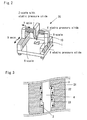
FIG. 3 is an enlarged view showing a pressure which acts on a probe body in a pressing space of the micro surface shape measurement probe ofFIG. 1 ; -
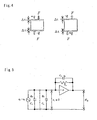
FIG. 4 is a diagram showing a principle of measurement of a load which acts on a piezoelectric ceramic; -
FIG. 5 is a diagram showing a charge amplification circuit of an FET input; -
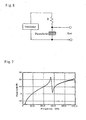
FIG. 6 is a circuit diagram for measuring a resonance characteristic of a piezoelectric ceramic; -
FIG. 7 is a graph showing, in a power level value, an impedance change of the piezoelectric ceramic in a case where a sinusoidal frequency of an oscillator is swept from 10 Hz to 100 kHz in the circuit ofFIG. 6 ; -
FIG. 8 is a graph showing an impedance (power level value) change of a piezoelectric ceramic with respect to a frequency in a case where different loads act on the piezoelectric ceramic to which a constant voltage has been applied; -
FIG. 9 is a diagram showing a probe member in which a distant end ball is formed integrally with a shaft portion; -
FIG. 10 is a diagram showing a probe member which is elastically deformed by a contact pressure according to the invention; -
FIG. 11 is a diagram showing a constitution in which contact is sensed by use of laser light reflected by a contact point between a probe member and an object to be measured according to the invention; -
FIG. 12 is a diagram showing a constitution to sense a contact pressure between a probe member and an object based on a phase difference between laser light emitted to a contact point and laser light reflected by the contact point and returned through the probe member according to the invention; -
FIG. 13A is a diagram showing a constitution example of a pressing device using a magnetic force; and -
FIG. 13B is a cross sectional view, taken along the A-A arrow line ofFIG. 13A . - Preferred embodiments of the present invention will be described with reference to the drawings, in particular
Figs 9 to 12 . It is to be noted that in the drawings, common parts are denoted with the same reference numerals, and redundant description is omitted. - There will be described a micro surface shape measurement probe in the following order:
- 1. Outline of Micro Surface Shape Measurement Probe;
- 2. Description of devices of Micro Surface Shape Measurement Probe;
- 3. Application of Piezoelectric Ceramic;
- 4. Use Method of Piezoelectric Ceramic;
- 5. A Probe member according to the invention; and
- 6. Pressing Device using Magnetic Force.
-
FIG. 1 is the whole constitution diagram of a micro surfaceshape measurement probe 10. As shown inFIG. 1 , the micro surfaceshape measurement probe 10 includes aprobe shaft 4 having aprobe member 2 on a distant end thereof; a probe body which is a support structure for movably supporting theprobe shaft 4; a pressing device (e.g., gas supply means 25, 26) which applies a pressing force to theprobe shaft 4 to urge and move theprobe shaft 4 toward anobject 1 to be measured; a micro force measurement device (e.g., a piezoelectric ceramic 8a) which detects a micro contact pressure between theprobe member 2 and theobject 1 to be measured; acontrol device 9 which controls the pressing force of the pressing device based on the contact pressure detected by the micro force measurement device; and a displacement amount measuring device (e.g., alaser displacement meter 16 using laser interference) which measures a position of theprobe member 2 in contact with theobject 1 to be measured. It is to be noted thatFIG. 1 shows a case where theprobe shaft 4 is disposed in a vertical direction, but theprobe shaft 4 may be disposed in a horizontal direction or an oblique direction. - The operation of the micro surface
shape measurement probe 10 will briefly be described. - The pressing device presses the
probe shaft 4 toward theobject 1 to be measured, for example, in a vertical direction, to thereby bring theprobe member 2 of the distant end of theprobe shaft 4 into contact with theobject 1 to be measured. Especially, according to the embodiment of the present invention, as described later, the micro force measurement device can adjust the pressing force and the contact pressure with a precision of about 1 mgf. - Subsequently, the amount of the displacement of the
probe member 2 is measured by the displacement amount measuring device, in a state in which the contact between th.e probe member 2 and theobject 1 to be measured is maintained. The displacement amount measuring device is constituted of a reflectingmirror 12, light guide means (e.g., an optical fiber) 14, thelaser displacement meter 16, and the like. - A position of a point to be measured is measured, in accordance with a calculation processing of data of this amount of the displacement and a coordinate value of a Z-scale corresponding to a vertical direction of a
slider device 20 described later. That is, since there is a limitation in the measurement range of the amount of the displacement of theprobe member 2 because of the restriction on the stroke of theprobe shaft 4, an absolute position of the point to be measured is measured by the calculation processing of the amount of the displacement of theprobe member 2 and the amount of the displacement of the cooperating operation of theslider device 20 in the vertical direction (Z-axis direction). - The reflecting
mirror 12 is a plane mirror disposed in anenlarged diameter portion 17 on the rear end of theprobe shaft 4, perpendicular to the axis thereof. The light guide means 14 has a radiatingend surface 14a which faces the reflectingmirror 12 at a predetermined space therebetween. The light guide means 14 has plasticity and a sufficient length, and the other end surface of the light guide means 14 is connected to thelaser displacement meter 16 via an optical connector or the like. - The
laser displacement meter 16 includes, for example, a semiconductor laser, a light receiving element, an optical fiber coupler and the like, and radiates laser light toward the reflectingmirror 12 through the light guide means 14, so that it measures a position of the reflectingmirror 12 from reflected lights from the reflectingmirror 12 and the radiatingend surface 14a. - According to this constitution, the position of the reflecting
mirror 12, that is, the position of theprobe shaft 4, can be measured with a high precision by use of thelaser displacement meter 16. - As shown in
FIG. 2 , the micro surfaceshape measurement probe 10 is attached to theslider device 20 so as to be movable in the X-direction, the Y-direction and the Z-direction. Theslider device 20 moves the micro surfaceshape measurement probe 10 in a static pressure slide system in which a fluid (a gas such as air or a liquid such as oil) is used as a medium as shown inFIG. 2 . An X-coordinate value, a Y-coordinate value and a Z-coordinate value of the micro surfaceshape measurement probe 10 can be obtained by the X-scale, the Y-scale and the Z-scale of theslider device 20. In consequence, theprobe member 2 is scanned along the whole surface of the object to be measured to obtain surface shape data. - In the example of the arrangement of the
slider device 20 shown inFIG. 2 , theprobe member 2 is vertically disposed, but needless to say, theprobe member 2 may horizontally be disposed. - Moreover, a grinding tool, a cutting tool, a polishing tool and a discharge/electrochemical machining tool can be attached to the
same slider device 20, and thesame slider device 20 can perform grinding, cutting, polishing and discharge/electrochemical machining. - There will be described the constitution and the operation of devices of the micro surface shape measurement probe in more detail.
- The
probe shaft 4 has theprobe member 2 disposed at the distant end thereof for contacting theobject 1 to be measured, and theenlarged diameter portion 17 disposed on the rear end thereof and enlarged in the radial direction, and is disposed in ahollow portion 18 of the probe body. Thehollow portion 18 is formed in the vicinity of the center of the probe body in the axial direction of the body. As shown inFIG. 1 , when theprobe shaft 4 is disposed in thehollow portion 18 of the probe body,support spaces 19 andpressing spaces probe shaft 4 and the probe body. It is preferable that theprobe shaft 4 and thehollow portion 18 are formed into such shapes that theprobe shaft 4 does not freely rotate, but if they are formed into a rotation symmetric shape, fixed at a predetermined angle and used, the constitution is further effective. - Pressurized gas (compressed air or the like) is supplied from the periphery of the
probe shaft 4 to thesupport spaces 19 at a certain flow rate by gas supply means 24 (constituted of, e.g., an air source, a regulator, an electro pneumatic regulator, andchannels 24a disposed in the probe body). In consequence, theprobe shaft 4 is supported in thehollow portion 18 in a non-contact manner with respect to the probe body. - On the other hand, the pressurized gas is also supplied to the
pressing spaces channel FIG. 1 , steppedportions 3 are formed on theprobe shaft 4 so that they are positioned in thepressing spaces space 22, the pressure is applied to the steppedportion 3 by this pressurized gas, and theprobe shaft 4 is pressed downwards. When the pressurized gas is supplied to the otherpressing space 23, the pressure is applied to the steppedportion 3 by this pressurized gas, and theprobe shaft 4 is pressed upwards. When flow rates of the pressurized gases to be supplied to thepressing spaces probe shaft 4 in the vertical direction. It is to be noted that an excess pressurized gas is supplied to thepressing space 23 at a flow rate corresponding to a weight of theprobe shaft 4 to offset the influence of the weight of theprobe shaft 4. It is to be noted that the gas supply means 24, 26 and thechannels - In consequence, the pressing force to be applied to the
probe shaft 4 can be set to about 50 mgf. However, to obtain a further micro pressing force, that is, contact pressure, it is necessary to adjust the pressing force or the contact pressure further minutely below 50 mgf. Therefore, when the micro force measurement device is constituted using the piezoelectric ceramic 8a, it is possible to detect the pressing force and the contact pressure with a precision of about 1 mgf. In consequence, while theprobe member 2 is brought into contact with theobject 1 to be measured with a further micro pressing force as compared with a conventional technology, a cooperating control is performed along a Z-axis, and the contact is further scanned along the surface of theobject 1 to be measured in an X-Y plane. In consequence, highly precise surface shape measurement is realized. - According to the embodiment as shown in
FIG. 1 , the micro force measurement device has a piezoelectric ceramic 8a inserted in and pinched by the rear portion of the probe body, perpendicular to the axial direction, and aload detecting device 8b to detect a load which acts on this piezoelectric ceramic 8a. It is to be noted that in the example ofFIG. 1 , the piezoelectric ceramic 8a is incorporated in the probe body and a through hole for passing the laser light is formed in the center of the piezoelectric ceramic 8a, in cross section, but the piezoelectric ceramic 8a does not necessarily have any through hole, as long as the function of the piezoelectric sensor described later can be realized. In the present embodiment, the piezoelectric ceramic 8a is used as the piezoelectric sensor, but another appropriate piezoelectric sensor may be used. - In a state in which the
probe shaft 4 stands still in the non-contact manner with respect to the probe body by the gas supply means 25, 26, a weight of a portion of the probe body positioned below the piezoelectric ceramic 8a, and a force (total force of forces shown by arrows inFIG. 3 ) of the pressurized gas acting on the probe body by the fact that the gas supply means 25, 26 allow theprobe shaft 4 to float and stand still, are acting on the piezoelectric ceramic 8a. - From this state, when the flow rates of the pressurized gases supplied to the
pressing spaces probe shaft 4 downwards, the total force of the forces shown by the arrows inFIG. 3 (i.e., a reactive force from theprobe shaft 4 to the probe body) increases upwardly, and the load which acts on the piezoelectric ceramic 8a also increases in such a direction as to compress the piezoelectric ceramic 8a. - When the
probe shaft 4 is moved to bring theprobe member 2 into contact with theobject 1 to be measured, theprobe shaft 4 is subjected to the reactive force due to the contact between the contact and theobject 1 to be measured, but the total force of the forces shown by the arrows inFIG. 3 (i.e., the reactive force from theprobe shaft 4 to the probe body) does not change as long as the pressing force is not changed. However, this is a case where air resistance and the like are ignored. - It is possible to minutely adjust the contact pressure between the
probe member 2 and theobject 1 to be measured, by using this relation between the load of the piezoelectric ceramic 8a and the pressing force. That is, a difference between the load which acts on the piezoelectric ceramic 8a at a time when theprobe shaft 4 is allowed to float and stand still by the gas supply means 25, 26 and the load which acts on the piezoelectric ceramic 8a at a time when theprobe shaft 4 is pressed downwards by the gas supply means 25, 26 corresponds to a downward pressing force, that is, the contact pressure between theprobe member 2 and theobject 1 to be measured. - Therefore, the
control device 9 can control the pressing force of the pressing device, while thecontrol device 9 performs the cooperating control in the Z-axis, based on a detected load value from theload detecting device 8b. - The load measurement by the piezoelectric ceramic 8a can be performed with a precision of about 1 mgf which is much smaller than a conventional technology precision of about 50 mgf. Therefore, when the piezoelectric ceramic 8a is incorporated in the probe body, the contact pressure can be adjusted with a precision of about 1 mgf.
- Next, there will be described use of the piezoelectric ceramic.
- First, characteristics of the piezoelectric ceramic will briefly be described.
-
FIG. 4 is a diagram showing a principle of load measurement performed by the piezoelectric ceramic. As shown inFIG. 4 , when a load F acts on the piezoelectric ceramic, electric charges +q, -q having different polarities are generated in the surfaces of electrodes, respectively. An amount of the generated electric charges is proportional to the amplitude of the load F which acts, and the polarity is determined by the direction of the load. Assuming that a piezoelectric constant is d, a relation between the load F and the electric charge q is represented by [Equation 1].
wherein d is a piezoelectric constant. - The thickness t of the element changes by Δt in accordance with the load F. The relation between the displacement Δt and the electric charge is represented by [Equation 2].

wherein A is an area of the element, t is the thickness of the element, Y is the Young's modulus, and Y = Ft/AΔt. - A voltage V generated between the electrodes is V = q/C, C is a capacity between the electrodes, and C = εA/t. Assuming that an output voltage is Vo, [Equation 3] is obtained.

wherein g is an element constant, and p is a force applied to the element. - The piezoelectric ceramic itself exhibits an idealistic characteristic in measurement of the load or the force. However, an insulation resistance of the piezoelectric ceramic itself is very large. Therefore, to precisely measure the voltage generated between the electrodes of the piezoelectric ceramic, it is necessary to use an amplifier having a large input resistance approximately equal to the insulation resistance. As this type of amplifier, a charge amplifier for a micro current has heretofore been used. This amplifier is determined in accordance with a type of a semiconductor for use in an input stage. The input stage of a general operational amplifier is a bipolar transistor circuit, and it cannot be used since the input resistance is small. Among usable charge amplification circuits, the most frequently used circuit is J-FET or MOS-FET.
-
FIG. 5 shows a charge amplification circuit of an FET input, and the circuit ofFIG. 5 is an operational amplifier in principle. - It is assumed that an input voltage is ei and an output voltage is eo. It is also assumed that an electric charge to be stored in a feedback capacity CF is qF and electric charges to be stored in an inner capacity C0 of the piezoelectric ceramic and a distribution capacity CC of a cable is q0. When it is assumed that a feedback resistance RF is very large, all the charges generated from the piezoelectric ceramic are stored in the input capacity (C0+CC) and the feedback capacity CF.
- From the relation of [Equation 4], [Equation 5] is obtained.


- Assuming that an increase ratio A is A >> 1, [Equation 6] is obtained.

- Therefore, the output voltage eo is proportional to the generated charge q. When a micro current flows through the feedback capacity CF to generate a direct voltage between CF terminals, an operation point of the amplifier gradually moves, and finally an output of the amplifier is sometimes saturated. Therefore, the feedback resistance RF of
FIG. 5 works so as to eliminate this saturation. On the other hand, in the amplifier, a cut-off frequency fC is dominated by time constants of RF and CF. The cut-off frequency is represented by [Equation 7].
- However, even when the piezoelectric ceramic is used, a large amount of the charge is generated, but it is difficult to measure a static force and a usually moderately fluctuating force or pressure. This problem occurs owing to influences of a small capacity of a connection cable of the piezoelectric ceramic and a low insulation resistance of an amplifier input circuit. In addition, the problem is dominated by a surrounding environment such as temperature or humidity as a cause for leakage.
- For example, assuming that the insulation resistance is Rin, an amplifier output is represented by [Equation 8].

- As seen from [Equation 8], when a stepped force is applied to the piezoelectric ceramic, the output voltage eo is output in accordance with the amplitude of the force, and then the output voltage eo exponentially drops in accordance with a time constant τ. It is to be noted that in a case where a small force is measured, since a sensitivity of the amplifier needs to be increased, a small value of the feedback capacity CF of the amplifier is selected. As a result, the output voltage eo drops fast, and it is difficult to calibrate a static force. That is, the piezoelectric ceramic has a characteristic that the measurement of the load by use of a piezoelectric effect can be realized with a high sensitivity and a high response. However, when a certain load is applied to the element and the element is allowed to stand for a long time, the output voltage eo drops and the sensitivity is not obtained finally. In other words, an only pulsating load can be measured.
- To solve the problem, the piezoelectric ceramic is used by the following method.
-
FIG. 6 is a circuit diagram for obtaining a resonance characteristic of the piezoelectric ceramic. InFIG. 6 , in a state in which there is not any restriction on the piezoelectric ceramic and the ceramic can be freely deformed, a certain voltage is applied between opposite polar plates of the piezoelectric ceramic from an oscillator. A resistance R sufficiently larger than an impedance of the piezoelectric ceramic is connected in series, and a voltage between opposite ends of the piezoelectric ceramic is measured. -
FIG. 7 is a graph showing that a sinusoidal frequency of the oscillator is swept from 10 Hz to 100 kHz (the abscissa), and showing, in a power level value (the ordinate), an impedance change of the piezoelectric ceramic. A resonance frequency is in the vicinity of about 52.6 kHz, and an antiresonant frequency appears in the vicinity of about 55.0 kHz. - The piezoelectric ceramic has this characteristic. Therefore, when the piezoelectric ceramic comes close to a mechanical resonance point, an elastic strain increases. This is piezoelectrically reflected, and a piezoelectric article is increasingly polarized. As a result, an electric capacity increases. In the resonance point, the increase of the electric capacity reaches its top, and the impedance of the piezoelectric ceramic indicates a minimum value. Thus, as the amplifier in which the piezoelectric ceramic has a sufficiently low impedance in the vicinity of the resonance frequency and the voltage between the opposite ends of the piezoelectric ceramic is amplified, a charge amplifier in which an initial stage is constituted of a high input resistance is not required, and a general amplifier is sufficiently used.
- Furthermore, the following experiment was performed.
- One of electrode surfaces of a piezoelectric ceramic was fixed to a metal plate with an adhesive, the other electrode surface of the piezoelectric ceramic was constituted as a free end surface, and a load of 0.98 N was put on this free end surface. While a frequency was swept, a constant current was applied between the opposite electrodes. At this time, the voltage between the opposite electrodes of the piezoelectric ceramic was measured. As a result, a change shown in
FIG. 8 was obtained. Next, a load of 9.8 N was put on the free end surface of the piezoelectric ceramic, and a similar experiment was performed. This result is also shown inFIG. 8 . - As shown in
FIG. 8 , when the load is applied, the resonance point shifts to a higher frequency, and a frequency change appears. In a case where there is supplied, between the opposite electrodes of the piezoelectric ceramic, a certain voltage or a certain current having a frequency fixed in the vicinity of 51.5 kHz in which the impedance rapidly changes, a resonance characteristic changes in accordance with the amplitude of the load. In consequence, the impedance between the opposite electrodes of the piezoelectric ceramic also changes. At this time, the impedance is converted into a voltage as a sensor output by use of a load sensor. Therefore, a sensor signal can be processed with an alternating-current amplifier, and a temperature characteristic of the sensitivity depends on an only temperature characteristic of the piezoelectric ceramic. - Therefore, as shown in
FIG. 1 , when the certain voltage having the fixed frequency is applied between the opposite polar plates of the piezoelectric ceramic 8a inserted in and pinched by theprobe body 21 as a support structure and the impedance between the polar plates of the piezoelectric ceramic 8a is measured, stable load measurement can be performed. Preferably, while there is applied, between the opposite polar plates of the piezoelectric sensor, the certain voltage having the frequency fixed in the vicinity of the resonance frequency of the piezoelectric ceramic 8a, and the impedance between the polar plates of the piezoelectric ceramic 8a is measured, stable load measurement can be performed. Preferably, while the certain voltage having the frequency fixed in the vicinity of the resonance frequency of the piezoelectric ceramic 8a is applied between the opposite polar plates of the piezoelectric sensor, the impedance between the polar plates of the piezoelectric ceramic 8a is measured. In consequence, the amplifier in which the initial stage is the high input resistance does not have to be used, and the load measurement of the piezoelectric ceramic 8a can be performed with a general amplifier. - Therefore, the impedance change of the piezoelectric ceramic 8a can be processed with the alternating-current amplifier, and the contact pressure between the
probe member 2 and theobject 1 to be measured can be measured with an excellent sensitivity of about 1 mgf as described above. It is to be noted that voltage supply means for applying an alternating voltage between the piezoelectric ceramics and impedance detection means for converting the impedance of the piezoelectric ceramic into a voltage to detect the impedance constitute a load measuring device. As the voltage supply means and the impedance detection means, known appropriate means can be used. - The
probe member 2 can be constituted of a micro probe having a conical or pyramid shape, and it is preferable that the distant end of the probe member is formed into a pointed shape or a spherical shape. It is also preferable that the micro probe is ground with a conductive grindstone dressed by electrolysis or ultra-precisely cut with a diamond tool. In a case where the probe of the present invention is used in on-machine measurement, when processing is performed on the same machine, highly precise processing is realized. In consequence, a highly precisely processed surface can be obtained. Especially, in a case where theprobe member 2 is processed while the contact is rotated centering on the axial center, since a shape precision (an error) of theprobe member 2 has a symmetric property with respect to a rotation shaft, dependence of measurement data on the contact position of theprobe member 2 is reduced, and the precision of the measurement using theprobe member 2 can be increased. Moreover, when the shape precision of theprobe member 2 is obtained beforehand by another measurement means, it is possible to predict the precision of the measurement using theprobe member 2. - Especially, in a case where the distant end of the
probe member 2 is formed into the spherical shape, when the distant end ball is processed, molded and then attached to theprobe member 2, there is a problem that there occurs not only a fluctuation of sphericity of each formed distant end ball but also an attachment error of the distant end ball. Therefore, as shown inFIG. 9 , thedistant end ball 2a is processed and molded integrally with theshaft portion 2b. Therefore, since the only distant end ball is not independently processed and molded and the distant end is formed into the spherical shape integrally with theshaft portion 2b of theprobe member 2, the attachment error is eliminated and the above problem can be solved. It is to be noted that inFIG. 9 ,reference numeral 32 is a male screw portion to be attached to theprobe shaft 4. Needless to say, without using any screwy, the contact may be formed into a tapered or non-axially-symmetric shape and mechanically tightened, or the contact may be thightened by a magnetic force. - It is also preferable that the
probe member 2 is coated preferably with a hard thin coating (e.g., DLC, TiN, TiC or the like). In consequence, a wear resistance of theprobe member 2 increases, a wear coefficient of the distant end portion of theprobe member 2 can be selected and adjusted, and an effect is produced at a time when the contact is brought into contact with theobject 1 to be measured. - Next, there will be described specific constitution examples of the
probe member 2 according to the invention. - To control the contact pressure between the
probe member 2 and the object 1-to be measured with a higher precision, theprobe member 2 is elastically displaced by the contact pressure, the contact pressure is calculated from this elastic displacement and a spring constant of theprobe member 2, and thecontrol device 9 can control the pressing device based on this calculated contact pressure to adjust the pressing force. In consequence, the contact pressure can further minutely be adjusted as compared with a conventional example. - This constitution example is shown in
FIG. 10 . As shown inFIG. 10 , anelastic article 2c made of a rubber or a (hollow) elastic resin is sandwiched between theprobe member 2 and theprobe shaft 4 to connect the contact to the shaft. Furthermore, areflective surface 2d of theprobe shaft 4 directed rearwards in the axial direction is formed on the back surface of theprobe member 2. - With the
probe member 2 constituted in this manner, ahollow portion 4a is formed in the central part of theprobe shaft 4, extending in the axial direction. Instead, the central part of theprobe shaft 4 may be formed of a transparent material such as glass, extending in the axial direction. A laser displacement meter similar to the abovelaser displacement meter 16 emits laser light from a radiating end surface toward thereflective surface 2d through thehollow portion 4a or a transparent material portion of thisprobe shaft 4, and measures a position of thereflective surface 2d from the reflected light from the radiating end surface and thereflective surface 2d. - Moreover, a probe distant end portion (i.e., the probe member 2) may be constituted of a transparent and hard medium such as sapphire, ruby or hard glass, without using the
reflective surface 2d, as shown inFIG. 11 , so that the laser light may be directed as it is from the inside toward the probe distant end portion and reflected by a contact point between the probedistant end portion 2 and theobject 1 to be measured. By detecting the reflected laser light, it is possible to detect the contact between theobject 1 to be measured and the probedistant end portion 2. In order to reduce the impact and the contact pressure due to the contact between the probe and theobject 1 to be measured before the measurement and control of the pressing force are performed by the piezoelectric element, the contact detection can be performed using the light. This is effective for avoiding surface damages on thedistant end portion 2 and theobject 1 to be measured. Thus, thelaser displacement meter 16 can constitute a contact sensing device which irradiates the contact point between theprobe member 2 and theobject 1 to be measured with the laser light through the contact and which detects the laser light reflected by the contact point to sense contact between theprobe member 2 and theobject 1 to be measured. It is to be noted that as shown inFIG. 11 , the laser light radiated to portions other than the contact point is radiated to the outside of the probe member. - Furthermore, in this case, as shown by the broken line in
FIG. 12 , owing to the contact pressure applied to the probedistant end portion 2 made of the transparent medium, the probedistant end portion 2 is deformed, a stress is generated in the probe and a refractive index of the probedistant end portion 2 changes. An optical path change occurs in the form of synergy action of this deformation of the probedistant end portion 2 and the refractive index change of the probedistant end portion 2. By detecting such an optical path change by the contact sensing device (e.g., the laser displacement meter 16), the pressing force can be detected and controlled. This optical path change can be detected, by measuring a phase difference between incident laser light and reflected laser light reflected by the contact point (shown by the broken line ofFIG. 12 ) by thelaser displacement meter 16. The contact pressure can be detected from the detected optical path change. It is to be noted that a relation between the phase difference and the contact pressure may be obtained beforehand using the pressing device or the micro force measurement device described in the present specification or another appropriate measurement device, and the contact pressure can be detected using the obtained relation. - Thus, if the contact or the contact pressure is sensed by the contact sensing device, any damage of the surfaces of the probe
distant end portion 2 and theobject 1 to be measured can be avoided, by performing such an control by thecontrol device 9 that the pressing force of the pressing device is not increased or decreased. - The amount of the elastic displacement can be obtained from the position of the
reflective surface 2d obtained in this manner, and the position of theenlarged diameter portion 17 of theprobe shaft 4 obtained by thelaser displacement meter 16. The contact pressure can be calculated from this amount of the elastic displacement and the spring constant of the elastic article. - According to this invention, instead of the piezoelectric ceramic 8a, the micro force measurement device is constituted of the
reflective surface 2d, the laser displacement meter, and the calculating device which calculates the contact pressure from the detected value of the laser displacement meter and the spring constant of theelastic article 2c - Moreover, the pressing device using the pressurized gas has been described above, but the present invention is not limited to this device, and another device may be used.
- For example, as shown in
FIGS. 13A and 13B , the pressing device may use a magnetic force.FIG. 13A is a side cross sectional view of theprobe body 21 in which the pressing device using the magnetic force is incorporated, andFIG. 13B is a cross sectional view, taken along the A-A arrow line ofFIG. 13A . As shown inFIGS. 13A and 13B , in order to support theprobe shaft 4 in a non-contact manner from theprobe body 21, a plurality of permanent magnets are arranged betweennonmagnetic plates 61 in theprobe shaft 4, and a plurality of N-poles 52 are arranged at appropriate intervals on the surface of thehollow portion 18 of theprobe body 21 as shown inFIG. 13A . In consequence, theprobe shaft 4 can be kept in the non-contact state from theprobe body 21 by the magnetic force which works between the plurality of permanent magnets and the N-poles 52 on the surface of thehollow portion 18 in theprobe shaft 4. - Furthermore, in order to urge and move the
probe shaft 4 in the vertical direction, the permanent magnets are arranged so that N-poles 53 are exposed externally from theenlarged diameter portions 17 on the rear end and the distant end of theprobe shaft 4 in a vertical axis direction, respectively, andpressing coils 54 are arranged in positions facing these N-poles 53 in theprobe body 21. According to this constitution, a current flowing through thepressing coil 54 on the distant end and a current flowing through thepressing coil 54 on the rear end are separately controlled to allow the magnetic force to act between the N-pole 53 and thepressing coil 54 which face each other in the vertical direction. In consequence, theprobe shaft 4 is supported and moved in the vertical direction. The influence of the weight of theprobe shaft 4 is offset by current adjustment of thepressing coil 54. Another constitution is similar to that of the above embodiments. In the example ofFIGS. 13A and 13B , the N-poles 53 and thepressing coils 54 constitute the pressing device. - In addition, here, even if shown N-poles and S-poles are arranged in reverse, needless to say, a similar operating function can be obtained.
- Moreover, when a static electric force is used instead of the magnetic force, that is, when portions corresponding to the above two magnetic poles are charged into + and -, the similar operating function can be obtained. Moreover, the magnetic force may partly be used, the static electric force may partly be used, and the forces may be combined.
Claims (2)
- A micro surface shape measurement probe (10) comprising:a probe shaft (4) having at a distant end thereof a probe member (2) for contacting an object (1) to be measured;a probe body provided with support means for movably supporting the probe shaft (4) in a non-contact manner;a pressing device (25, 26) for pressing and moving the probe shaft (4) toward the object (1) to be measured;a contact sensing device (16) for sensing contact between the probe member (2) and the object (1) by irradiating a contact point between the probe member (2) and the object (1) with laser light through the probe member (2) and detecting the laser light reflected by the contact point;a contact sensing device (16) for sensing a contact pressure between the probe member (2) and the object (1) by irradiating the contact point between the probe member (2) and the object (1) with laser light through the probe member (2) and detecting the laser light reflected by the contact point;a control device (9) for adjusting the pressing force applied by the pressing device (25, 26) based on the contact pressure detected by the contact sensing device (16); anda displacement amount measuring device for measuring a position of the probe member (2) in contact with the object (1) to be measured under the pressing force adjusted by the control device (9).
- The micro surface shape measurement probe according to claim 1, wherein the contact sensing device (16) for sensing the contact pressure between the probe member (2) and the object (1) is designed to sense the contact pressure on the basis of a phase difference between laser light emitted to the contact point between the probe member (2) and the object (1) and laser light reflected by the contact point and returned through the probe member (2).
Applications Claiming Priority (2)
| Application Number | Priority Date | Filing Date | Title |
|---|---|---|---|
| JP2005349468A JP4933775B2 (en) | 2005-12-02 | 2005-12-02 | Micro surface shape measurement probe |
| EP20060024833 EP1793197B1 (en) | 2005-12-02 | 2006-11-30 | Measuring probe with a plurality of concentrically arranged cantilevers |
Related Parent Applications (1)
| Application Number | Title | Priority Date | Filing Date |
|---|---|---|---|
| EP20060024833 Division EP1793197B1 (en) | 2005-12-02 | 2006-11-30 | Measuring probe with a plurality of concentrically arranged cantilevers |
Publications (3)
| Publication Number | Publication Date |
|---|---|
| EP1909060A2 EP1909060A2 (en) | 2008-04-09 |
| EP1909060A3 EP1909060A3 (en) | 2008-04-23 |
| EP1909060B1 true EP1909060B1 (en) | 2009-05-06 |
Family
ID=37728169
Family Applications (2)
| Application Number | Title | Priority Date | Filing Date |
|---|---|---|---|
| EP20080000507 Not-in-force EP1909060B1 (en) | 2005-12-02 | 2006-11-30 | Micro surface shape measuring probe |
| EP20060024833 Not-in-force EP1793197B1 (en) | 2005-12-02 | 2006-11-30 | Measuring probe with a plurality of concentrically arranged cantilevers |
Family Applications After (1)
| Application Number | Title | Priority Date | Filing Date |
|---|---|---|---|
| EP20060024833 Not-in-force EP1793197B1 (en) | 2005-12-02 | 2006-11-30 | Measuring probe with a plurality of concentrically arranged cantilevers |
Country Status (5)
| Country | Link |
|---|---|
| US (1) | US7685733B2 (en) |
| EP (2) | EP1909060B1 (en) |
| JP (1) | JP4933775B2 (en) |
| KR (1) | KR101268043B1 (en) |
| DE (2) | DE602006006680D1 (en) |
Cited By (1)
| Publication number | Priority date | Publication date | Assignee | Title |
|---|---|---|---|---|
| CN106595942A (en) * | 2016-07-25 | 2017-04-26 | 北京卫星环境工程研究所 | Dynamic measuring device of micro force |
Families Citing this family (41)
| Publication number | Priority date | Publication date | Assignee | Title |
|---|---|---|---|---|
| DE102005007327B4 (en) * | 2005-02-17 | 2010-06-17 | Continental Automotive Gmbh | Circuit arrangement and method for operating an injector arrangement |
| DE102007005222A1 (en) * | 2006-02-03 | 2007-08-09 | Ceramtec Ag Innovative Ceramic Engineering | Use of piezoceramic transducers to control the machining of workpieces |
| US7849738B2 (en) * | 2006-03-13 | 2010-12-14 | Sonoplot, Inc. | Device for detecting interaction with an object |
| JP4677493B2 (en) * | 2008-01-22 | 2011-04-27 | キヤノン株式会社 | Piezoelectric vibration type force sensor |
| JP4291394B1 (en) | 2008-03-12 | 2009-07-08 | ファナック株式会社 | Contact-type measuring device |
| CN101368856B (en) * | 2008-06-30 | 2010-06-02 | 中南大学 | Stress collection device and stress monitoring system for column of giant die forging hydraulic press |
| KR100889846B1 (en) * | 2008-08-21 | 2009-03-20 | 김유찬 | Automatic weld line tracker |
| RU2605816C9 (en) * | 2008-10-09 | 2017-05-10 | Ньюкасл Инновейшн Лимитед | Positioning system and method |
| JP2010105063A (en) * | 2008-10-28 | 2010-05-13 | Fanuc Ltd | Method for measuring workpiece dimensions using onboard measuring device for temperature drift correction, and machine tool including the onboard measuring device |
| CN101728973A (en) * | 2008-10-31 | 2010-06-09 | 鸿富锦精密工业(深圳)有限公司 | Driving device and overload protection method thereof |
| JP4850265B2 (en) * | 2009-03-12 | 2012-01-11 | パナソニック株式会社 | Probe for shape measuring device and shape measuring device |
| JP5336279B2 (en) * | 2009-07-08 | 2013-11-06 | 株式会社ミツトヨ | Surface texture measuring device and roundness measuring device |
| CN101762351B (en) * | 2010-01-07 | 2011-10-05 | 重庆交通大学 | A Method for Measuring the Tension Force of Tie Rods in Large Buildings |
| JP4875180B2 (en) | 2010-03-25 | 2012-02-15 | ファナック株式会社 | Contact-type measuring device with fine contact force adjustment mechanism |
| DE102010026892A1 (en) | 2010-04-09 | 2011-10-13 | Stotz Feinmesstechnik Gmbh | Device for measuring objects |
| JP5879621B2 (en) * | 2010-06-02 | 2016-03-08 | 国立大学法人 熊本大学 | Micromaterial strain measuring apparatus and method |
| GB201012249D0 (en) * | 2010-07-21 | 2010-09-08 | Renishaw Plc | Metrology apparatus |
| CN102169035B (en) * | 2010-12-22 | 2012-06-27 | 中国科学院广州能源研究所 | Torsional high-accuracy micro-thrust measuring system |
| JP5728788B2 (en) * | 2011-02-15 | 2015-06-03 | 国立研究開発法人物質・材料研究機構 | Ultrasonic fatigue test method and test apparatus under high temperature conditions |
| US8701511B2 (en) * | 2011-03-22 | 2014-04-22 | International Business Machines Corporation | Inert gas delivery system for electrical inspection apparatus |
| DE102011005934A1 (en) * | 2011-03-23 | 2012-09-27 | Continental Automotive Gmbh | Method for determining the force relationships on the nozzle needle of a directly driven piezo injector |
| CN107255462B (en) | 2011-07-08 | 2019-07-23 | 卡尔蔡司工业测量技术有限公司 | Measure workpiece coordinate when error correction and/or avoid |
| CN103175636B (en) * | 2012-12-18 | 2015-02-18 | 大连理工大学 | Load-sharing piezoelectric multi-dimensional force measuring device and method for manufacturing the same |
| US20140207406A1 (en) * | 2013-01-22 | 2014-07-24 | General Electric Company | Self-directed inspection plan |
| GB2512289B (en) * | 2013-03-22 | 2018-12-26 | Ross Nedwell Jeremy | A device for determining the characteristic impedance spectrum of a token |
| JP6141713B2 (en) * | 2013-07-23 | 2017-06-07 | 上田日本無線株式会社 | Method for obtaining structural information inside a living body |
| LT6206B (en) | 2013-10-04 | 2015-08-25 | Aleksandro Stulginskio Universitetas | Device for contact zone diagnostics of piezoelectric motors |
| KR200477422Y1 (en) * | 2013-11-28 | 2015-06-05 | 한전케이피에스 주식회사 | Gauge for Measuring Inner Diameter |
| JP2016099221A (en) * | 2014-11-21 | 2016-05-30 | 株式会社小野測器 | Probe device, laser measurement device, and laser measurement system |
| CN105436280B (en) * | 2015-12-24 | 2018-05-29 | 安拓锐高新测试技术(苏州)有限公司 | A kind of probe stamping equipment |
| US20180080839A1 (en) * | 2016-09-21 | 2018-03-22 | Qualcomm Incorporated | Piezoelectric material test probe and method |
| RU2657110C2 (en) * | 2016-11-08 | 2018-06-08 | федеральное государственное бюджетное образовательное учреждение высшего образования "Алтайский государственный технический университет им. И.И. Ползунова" (АлтГТУ) | Distributed piezoelectric power converter |
| CN107101753B (en) * | 2017-06-29 | 2023-08-11 | 四川西交路安科技有限公司 | Quartz sensor for horizontal force detection and horizontal force detection device |
| JP7213059B2 (en) * | 2018-10-24 | 2023-01-26 | 株式会社ミツトヨ | Surface texture measuring device and its control method |
| CN120009582A (en) * | 2019-02-21 | 2025-05-16 | 维耶尔公司 | Probe structures for microdevice inspection |
| CN109683003B (en) * | 2019-02-22 | 2020-12-01 | 西安微电子技术研究所 | Self-protection test meter pen with protection function and manufacturing method thereof |
| CN111928748B (en) * | 2019-05-13 | 2022-05-13 | 安徽科瑞特模塑有限公司 | General detection tool for machining vehicle air guide sleeve |
| CN215984490U (en) * | 2021-10-08 | 2022-03-08 | 宁德时代新能源科技股份有限公司 | Pole piece wavy edge detection device |
| CN114966139B (en) * | 2022-07-22 | 2022-10-25 | 威海双丰物探设备股份有限公司 | Impedance matcher parameter measuring device for hydrophone |
| CN115711690B (en) * | 2022-10-27 | 2026-01-13 | 苏州大学 | Target ball adsorption and micro-force detection device based on capacitance sensor |
| CN115855353B (en) * | 2022-11-29 | 2024-08-16 | 中国核电工程有限公司 | Displacement control device and method, pressure sensor production method and equipment |
Family Cites Families (30)
| Publication number | Priority date | Publication date | Assignee | Title |
|---|---|---|---|---|
| US2558563A (en) * | 1948-10-29 | 1951-06-26 | Gen Electric | Piezoelectric strain gauge |
| GB1393035A (en) * | 1971-07-09 | 1975-05-07 | Olivetti & Co Spa | Precision measuring apparatus with aerostatic bearings |
| DE2242355C2 (en) * | 1972-08-29 | 1974-10-17 | Fa. Carl Zeiss, 7920 Heidenheim | Electronic multi-coordinate probe |
| JPS5278483A (en) * | 1975-12-25 | 1977-07-01 | Toray Industries | Method of measuring force |
| JPS5818133A (en) * | 1981-07-24 | 1983-02-02 | Matsushita Electric Ind Co Ltd | pressure sensor |
| JPS58106404A (en) * | 1981-12-18 | 1983-06-24 | Mitsutoyo Mfg Co Ltd | Displacement measuring device |
| JPS60104201A (en) * | 1983-11-10 | 1985-06-08 | Japan Atom Energy Res Inst | Minute displacement measuring instrument |
| CA1276710C (en) * | 1983-11-30 | 1990-11-20 | Kazuo Asakawa | Robot force controlling system |
| JPS63197733A (en) * | 1987-02-09 | 1988-08-16 | 株式会社イナックス | Flash toilet |
| JP2548012B2 (en) * | 1987-07-29 | 1996-10-30 | 京セラ株式会社 | Touch sensor |
| DE3920716C1 (en) * | 1989-06-24 | 1990-11-29 | Wild Leitz Gmbh, 6330 Wetzlar, De | |
| JP2661314B2 (en) * | 1990-03-07 | 1997-10-08 | 松下電器産業株式会社 | Shape measuring device and shape measuring method |
| JPH0469767A (en) * | 1990-07-10 | 1992-03-04 | Ricoh Co Ltd | Document generating device |
| JP2519823B2 (en) * | 1990-08-17 | 1996-07-31 | 株式会社東芝 | Displacement measuring device |
| EP0471371B1 (en) * | 1990-08-17 | 1995-04-12 | Kabushiki Kaisha Toshiba | Displacement-measuring apparatus |
| US5247751A (en) * | 1990-09-29 | 1993-09-28 | Nikon Corporation | Touch probe |
| DE4238139C2 (en) * | 1992-11-12 | 2002-10-24 | Zeiss Carl | The coordinate |
| JPH0862227A (en) * | 1994-08-18 | 1996-03-08 | Hitachi Ltd | Scanning probe microscope probe and microscope equipped with the same |
| US5765273A (en) * | 1995-09-22 | 1998-06-16 | Black & Decker Inc. | Drill press having pivotable table |
| JPH09251026A (en) * | 1996-03-15 | 1997-09-22 | Toshiba Corp | Scanning probe microscope |
| US5822877A (en) * | 1996-06-20 | 1998-10-20 | Brown & Sharpe Manufacturing Company | Multi-probe system for dimensional metrology |
| JPH11316119A (en) * | 1998-05-06 | 1999-11-16 | Ricoh Co Ltd | Contact load control device and shape measuring device using the same |
| JP4178600B2 (en) * | 1998-07-15 | 2008-11-12 | 株式会社デンソー | Load measuring device and load measuring element |
| DE60033272T2 (en) | 1999-03-03 | 2007-11-29 | Riken, Wako | PROBE-TYPE FORM-MEASUREMENT PROBE AND NC-MACHINING DEVICE AND FORM-MEASURING METHOD USING THE MEASURING TELEVISION |
| JP4253084B2 (en) * | 1999-04-08 | 2009-04-08 | 富士重工業株式会社 | Load measuring device |
| JP2000304529A (en) * | 1999-04-22 | 2000-11-02 | Ricoh Co Ltd | Probe device and shape measuring device |
| JP4526626B2 (en) * | 1999-12-20 | 2010-08-18 | 独立行政法人科学技術振興機構 | Electrical property evaluation equipment |
| EP1316778B1 (en) * | 2001-11-30 | 2007-07-25 | Tesa Sa | Touch probe and method of assembling a touch probe |
| JP4376592B2 (en) * | 2003-10-31 | 2009-12-02 | 株式会社リコー | Shape measuring device |
| JP4436665B2 (en) * | 2003-12-24 | 2010-03-24 | パナソニック株式会社 | Measuring probe and shape measuring method |
-
2005
- 2005-12-02 JP JP2005349468A patent/JP4933775B2/en not_active Expired - Fee Related
-
2006
- 2006-11-29 KR KR1020060118884A patent/KR101268043B1/en not_active Expired - Fee Related
- 2006-11-30 EP EP20080000507 patent/EP1909060B1/en not_active Not-in-force
- 2006-11-30 EP EP20060024833 patent/EP1793197B1/en not_active Not-in-force
- 2006-11-30 DE DE200660006680 patent/DE602006006680D1/en active Active
- 2006-11-30 DE DE200660002093 patent/DE602006002093D1/en active Active
- 2006-12-04 US US11/566,377 patent/US7685733B2/en not_active Expired - Fee Related
Cited By (2)
| Publication number | Priority date | Publication date | Assignee | Title |
|---|---|---|---|---|
| CN106595942A (en) * | 2016-07-25 | 2017-04-26 | 北京卫星环境工程研究所 | Dynamic measuring device of micro force |
| CN106595942B (en) * | 2016-07-25 | 2019-06-07 | 北京卫星环境工程研究所 | The dynamic measurement device of small power |
Also Published As
| Publication number | Publication date |
|---|---|
| DE602006006680D1 (en) | 2009-06-18 |
| US7685733B2 (en) | 2010-03-30 |
| DE602006002093D1 (en) | 2008-09-18 |
| KR101268043B1 (en) | 2013-05-28 |
| EP1793197B1 (en) | 2008-08-06 |
| JP2007155440A (en) | 2007-06-21 |
| US20070126314A1 (en) | 2007-06-07 |
| EP1793197A3 (en) | 2007-06-27 |
| EP1909060A3 (en) | 2008-04-23 |
| JP4933775B2 (en) | 2012-05-16 |
| EP1793197A2 (en) | 2007-06-06 |
| EP1909060A2 (en) | 2008-04-09 |
| KR20070058326A (en) | 2007-06-08 |
Similar Documents
| Publication | Publication Date | Title |
|---|---|---|
| EP1793197B1 (en) | Measuring probe with a plurality of concentrically arranged cantilevers | |
| US20030009898A1 (en) | Characterization of compliant structure force-displacement behavior | |
| JP5193337B2 (en) | Micro surface shape measurement probe | |
| CN101949804B (en) | Test method of electromagnetic micro-force tester based on flexible support technology | |
| EP1970714A1 (en) | Device including a contact detector | |
| CN116295105B (en) | Optical interference type micro-machined wafer surface morphology measuring device and measuring method | |
| US5414940A (en) | Contact position sensor using constant contact force control system | |
| CN105491492A (en) | Self-calibration silicon microphone device and self-calibration method | |
| CN102506688B (en) | Resistance strain thickness measuring device and measurement method thereof | |
| CN108680093B (en) | A focusing distance measuring device and measuring method in an optical focusing mechanism | |
| US20230057869A1 (en) | Resonant frequency-based magnetic sensor at veering zone and method | |
| Chetwynd et al. | A controlled-force stylus displacement probe | |
| Oiwa et al. | Three-dimensional touch probe using three fibre optic displacement sensors | |
| CN106644715B (en) | A portable scratch-in test system | |
| US5245872A (en) | Device for precise measurement of force | |
| CN119000880A (en) | Elastic modulus testing method and device for elastic piece | |
| CN104076826B (en) | The position calculating apparatus and position calculating method of actuator | |
| JP2853687B2 (en) | Surface property evaluation device | |
| JPH09229663A (en) | Stylus type film thickness measuring method and measuring device | |
| JP2004053299A (en) | Machine for measuring thickness in plate-like material work | |
| Broistedt et al. | Force transducer based on a geometric-optical displacement sensor | |
| JP2007085823A (en) | Hardness meter | |
| KR20070075632A (en) | Device for inspecting properties of thin film materials and positioning method | |
| JP2614645B2 (en) | Displacement measuring device | |
| JPH05107021A (en) | Surface shape measuring device |
Legal Events
| Date | Code | Title | Description |
|---|---|---|---|
| PUAI | Public reference made under article 153(3) epc to a published international application that has entered the european phase |
Free format text: ORIGINAL CODE: 0009012 |
|
| PUAL | Search report despatched |
Free format text: ORIGINAL CODE: 0009013 |
|
| AC | Divisional application: reference to earlier application |
Ref document number: 1793197 Country of ref document: EP Kind code of ref document: P |
|
| AK | Designated contracting states |
Kind code of ref document: A2 Designated state(s): AT BE BG CH CY CZ DE DK EE ES FI FR GB GR HU IE IS IT LI LT LU LV MC NL PL PT RO SE SI SK TR |
|
| AX | Request for extension of the european patent |
Extension state: AL BA HR MK RS |
|
| AK | Designated contracting states |
Kind code of ref document: A3 Designated state(s): AT BE BG CH CY CZ DE DK EE ES FI FR GB GR HU IE IS IT LI LT LU LV MC NL PL PT RO SE SI SK TR |
|
| AX | Request for extension of the european patent |
Extension state: AL BA HR MK RS |
|
| 17P | Request for examination filed |
Effective date: 20080610 |
|
| 17Q | First examination report despatched |
Effective date: 20080714 |
|
| GRAP | Despatch of communication of intention to grant a patent |
Free format text: ORIGINAL CODE: EPIDOSNIGR1 |
|
| AKX | Designation fees paid |
Designated state(s): DE GB |
|
| RIC1 | Information provided on ipc code assigned before grant |
Ipc: G01B 5/012 20060101AFI20081121BHEP Ipc: G01B 11/00 20060101ALI20081121BHEP |
|
| RTI1 | Title (correction) |
Free format text: MICRO SURFACE SHAPE MEASURING PROBE |
|
| GRAS | Grant fee paid |
Free format text: ORIGINAL CODE: EPIDOSNIGR3 |
|
| GRAA | (expected) grant |
Free format text: ORIGINAL CODE: 0009210 |
|
| AC | Divisional application: reference to earlier application |
Ref document number: 1793197 Country of ref document: EP Kind code of ref document: P |
|
| AK | Designated contracting states |
Kind code of ref document: B1 Designated state(s): DE GB |
|
| REG | Reference to a national code |
Ref country code: GB Ref legal event code: FG4D |
|
| REF | Corresponds to: |
Ref document number: 602006006680 Country of ref document: DE Date of ref document: 20090618 Kind code of ref document: P |
|
| PLBE | No opposition filed within time limit |
Free format text: ORIGINAL CODE: 0009261 |
|
| STAA | Information on the status of an ep patent application or granted ep patent |
Free format text: STATUS: NO OPPOSITION FILED WITHIN TIME LIMIT |
|
| 26N | No opposition filed |
Effective date: 20100209 |
|
| PGFP | Annual fee paid to national office [announced via postgrant information from national office to epo] |
Ref country code: DE Payment date: 20121128 Year of fee payment: 7 |
|
| PGFP | Annual fee paid to national office [announced via postgrant information from national office to epo] |
Ref country code: GB Payment date: 20121128 Year of fee payment: 7 |
|
| REG | Reference to a national code |
Ref country code: DE Ref legal event code: R119 Ref document number: 602006006680 Country of ref document: DE |
|
| GBPC | Gb: european patent ceased through non-payment of renewal fee |
Effective date: 20131130 |
|
| PG25 | Lapsed in a contracting state [announced via postgrant information from national office to epo] |
Ref country code: DE Free format text: LAPSE BECAUSE OF NON-PAYMENT OF DUE FEES Effective date: 20140603 |
|
| REG | Reference to a national code |
Ref country code: DE Ref legal event code: R119 Ref document number: 602006006680 Country of ref document: DE Effective date: 20140603 |
|
| PG25 | Lapsed in a contracting state [announced via postgrant information from national office to epo] |
Ref country code: GB Free format text: LAPSE BECAUSE OF NON-PAYMENT OF DUE FEES Effective date: 20131130 |