EP1903624A2 - Tunnel magnetoresistive sensor in which at least part of pinned layer is composed of CoFeB layer and method for manufacturing the tunnel magnetoresistive sensor - Google Patents
Tunnel magnetoresistive sensor in which at least part of pinned layer is composed of CoFeB layer and method for manufacturing the tunnel magnetoresistive sensor Download PDFInfo
- Publication number
- EP1903624A2 EP1903624A2 EP07018080A EP07018080A EP1903624A2 EP 1903624 A2 EP1903624 A2 EP 1903624A2 EP 07018080 A EP07018080 A EP 07018080A EP 07018080 A EP07018080 A EP 07018080A EP 1903624 A2 EP1903624 A2 EP 1903624A2
- Authority
- EP
- European Patent Office
- Prior art keywords
- magnetic
- layer
- subsublayer
- insulating barrier
- sublayer
- Prior art date
- Legal status (The legal status is an assumption and is not a legal conclusion. Google has not performed a legal analysis and makes no representation as to the accuracy of the status listed.)
- Granted
Links
Images





Classifications
-
- B—PERFORMING OPERATIONS; TRANSPORTING
- B82—NANOTECHNOLOGY
- B82Y—SPECIFIC USES OR APPLICATIONS OF NANOSTRUCTURES; MEASUREMENT OR ANALYSIS OF NANOSTRUCTURES; MANUFACTURE OR TREATMENT OF NANOSTRUCTURES
- B82Y10/00—Nanotechnology for information processing, storage or transmission, e.g. quantum computing or single electron logic
-
- B—PERFORMING OPERATIONS; TRANSPORTING
- B82—NANOTECHNOLOGY
- B82Y—SPECIFIC USES OR APPLICATIONS OF NANOSTRUCTURES; MEASUREMENT OR ANALYSIS OF NANOSTRUCTURES; MANUFACTURE OR TREATMENT OF NANOSTRUCTURES
- B82Y25/00—Nanomagnetism, e.g. magnetoimpedance, anisotropic magnetoresistance, giant magnetoresistance or tunneling magnetoresistance
-
- B—PERFORMING OPERATIONS; TRANSPORTING
- B82—NANOTECHNOLOGY
- B82Y—SPECIFIC USES OR APPLICATIONS OF NANOSTRUCTURES; MEASUREMENT OR ANALYSIS OF NANOSTRUCTURES; MANUFACTURE OR TREATMENT OF NANOSTRUCTURES
- B82Y40/00—Manufacture or treatment of nanostructures
-
- G—PHYSICS
- G01—MEASURING; TESTING
- G01R—MEASURING ELECTRIC VARIABLES; MEASURING MAGNETIC VARIABLES
- G01R33/00—Arrangements or instruments for measuring magnetic variables
- G01R33/02—Measuring direction or magnitude of magnetic fields or magnetic flux
- G01R33/06—Measuring direction or magnitude of magnetic fields or magnetic flux using galvano-magnetic devices
- G01R33/09—Magnetoresistive devices
- G01R33/093—Magnetoresistive devices using multilayer structures, e.g. giant magnetoresistance sensors
-
- G—PHYSICS
- G01—MEASURING; TESTING
- G01R—MEASURING ELECTRIC VARIABLES; MEASURING MAGNETIC VARIABLES
- G01R33/00—Arrangements or instruments for measuring magnetic variables
- G01R33/02—Measuring direction or magnitude of magnetic fields or magnetic flux
- G01R33/06—Measuring direction or magnitude of magnetic fields or magnetic flux using galvano-magnetic devices
- G01R33/09—Magnetoresistive devices
- G01R33/098—Magnetoresistive devices comprising tunnel junctions, e.g. tunnel magnetoresistance sensors
-
- G—PHYSICS
- G11—INFORMATION STORAGE
- G11B—INFORMATION STORAGE BASED ON RELATIVE MOVEMENT BETWEEN RECORD CARRIER AND TRANSDUCER
- G11B5/00—Recording by magnetisation or demagnetisation of a record carrier; Reproducing by magnetic means; Record carriers therefor
- G11B5/127—Structure or manufacture of heads, e.g. inductive
- G11B5/33—Structure or manufacture of flux-sensitive heads, i.e. for reproduction only; Combination of such heads with means for recording or erasing only
- G11B5/39—Structure or manufacture of flux-sensitive heads, i.e. for reproduction only; Combination of such heads with means for recording or erasing only using magneto-resistive devices or effects
- G11B5/3903—Structure or manufacture of flux-sensitive heads, i.e. for reproduction only; Combination of such heads with means for recording or erasing only using magneto-resistive devices or effects using magnetic thin film layers or their effects, the films being part of integrated structures
- G11B5/3906—Details related to the use of magnetic thin film layers or to their effects
-
- G—PHYSICS
- G11—INFORMATION STORAGE
- G11B—INFORMATION STORAGE BASED ON RELATIVE MOVEMENT BETWEEN RECORD CARRIER AND TRANSDUCER
- G11B5/00—Recording by magnetisation or demagnetisation of a record carrier; Reproducing by magnetic means; Record carriers therefor
- G11B5/127—Structure or manufacture of heads, e.g. inductive
- G11B5/33—Structure or manufacture of flux-sensitive heads, i.e. for reproduction only; Combination of such heads with means for recording or erasing only
- G11B5/39—Structure or manufacture of flux-sensitive heads, i.e. for reproduction only; Combination of such heads with means for recording or erasing only using magneto-resistive devices or effects
- G11B5/3903—Structure or manufacture of flux-sensitive heads, i.e. for reproduction only; Combination of such heads with means for recording or erasing only using magneto-resistive devices or effects using magnetic thin film layers or their effects, the films being part of integrated structures
- G11B5/3906—Details related to the use of magnetic thin film layers or to their effects
- G11B5/3909—Arrangements using a magnetic tunnel junction
-
- G—PHYSICS
- G11—INFORMATION STORAGE
- G11C—STATIC STORES
- G11C11/00—Digital stores characterised by the use of particular electric or magnetic storage elements; Storage elements therefor
- G11C11/02—Digital stores characterised by the use of particular electric or magnetic storage elements; Storage elements therefor using magnetic elements
- G11C11/16—Digital stores characterised by the use of particular electric or magnetic storage elements; Storage elements therefor using magnetic elements using elements in which the storage effect is based on magnetic spin effect
-
- H—ELECTRICITY
- H01—ELECTRIC ELEMENTS
- H01F—MAGNETS; INDUCTANCES; TRANSFORMERS; SELECTION OF MATERIALS FOR THEIR MAGNETIC PROPERTIES
- H01F10/00—Thin magnetic films, e.g. of one-domain structure
- H01F10/32—Spin-exchange-coupled multilayers, e.g. nanostructured superlattices
- H01F10/324—Exchange coupling of magnetic film pairs via a very thin non-magnetic spacer, e.g. by exchange with conduction electrons of the spacer
- H01F10/3254—Exchange coupling of magnetic film pairs via a very thin non-magnetic spacer, e.g. by exchange with conduction electrons of the spacer the spacer being semiconducting or insulating, e.g. for spin tunnel junction [STJ]
-
- H—ELECTRICITY
- H01—ELECTRIC ELEMENTS
- H01F—MAGNETS; INDUCTANCES; TRANSFORMERS; SELECTION OF MATERIALS FOR THEIR MAGNETIC PROPERTIES
- H01F41/00—Apparatus or processes specially adapted for manufacturing or assembling magnets, inductances or transformers; Apparatus or processes specially adapted for manufacturing materials characterised by their magnetic properties
- H01F41/14—Apparatus or processes specially adapted for manufacturing or assembling magnets, inductances or transformers; Apparatus or processes specially adapted for manufacturing materials characterised by their magnetic properties for applying magnetic films to substrates
- H01F41/30—Apparatus or processes specially adapted for manufacturing or assembling magnets, inductances or transformers; Apparatus or processes specially adapted for manufacturing materials characterised by their magnetic properties for applying magnetic films to substrates for applying nanostructures, e.g. by molecular beam epitaxy [MBE]
- H01F41/302—Apparatus or processes specially adapted for manufacturing or assembling magnets, inductances or transformers; Apparatus or processes specially adapted for manufacturing materials characterised by their magnetic properties for applying magnetic films to substrates for applying nanostructures, e.g. by molecular beam epitaxy [MBE] for applying spin-exchange-coupled multilayers, e.g. nanostructured superlattices
-
- H—ELECTRICITY
- H10—SEMICONDUCTOR DEVICES; ELECTRIC SOLID-STATE DEVICES NOT OTHERWISE PROVIDED FOR
- H10N—ELECTRIC SOLID-STATE DEVICES NOT OTHERWISE PROVIDED FOR
- H10N50/00—Galvanomagnetic devices
- H10N50/01—Manufacture or treatment
-
- H—ELECTRICITY
- H10—SEMICONDUCTOR DEVICES; ELECTRIC SOLID-STATE DEVICES NOT OTHERWISE PROVIDED FOR
- H10N—ELECTRIC SOLID-STATE DEVICES NOT OTHERWISE PROVIDED FOR
- H10N50/00—Galvanomagnetic devices
- H10N50/10—Magnetoresistive devices
-
- H—ELECTRICITY
- H01—ELECTRIC ELEMENTS
- H01F—MAGNETS; INDUCTANCES; TRANSFORMERS; SELECTION OF MATERIALS FOR THEIR MAGNETIC PROPERTIES
- H01F10/00—Thin magnetic films, e.g. of one-domain structure
- H01F10/08—Thin magnetic films, e.g. of one-domain structure characterised by magnetic layers
- H01F10/10—Thin magnetic films, e.g. of one-domain structure characterised by magnetic layers characterised by the composition
- H01F10/12—Thin magnetic films, e.g. of one-domain structure characterised by magnetic layers characterised by the composition being metals or alloys
- H01F10/13—Amorphous metallic alloys, e.g. glassy metals
- H01F10/132—Amorphous metallic alloys, e.g. glassy metals containing cobalt
Definitions
- the present invention relates to a tunnel magnetoresistive sensor that may be installed in a hard disk drive or be used as a magnetoresistive random access memory (MRAM), and more specifically, it relates to a tunnel magnetoresistive sensor that can achieve a high rate of resistance change ( ⁇ R/R) when Mg-O is used as an insulating barrier layer, and to a method for manufacturing the tunnel magnetoresistive sensor.
- MRAM magnetoresistive random access memory
- Tunnel magnetoresistive sensors generate a resistance change by utilizing a tunneling effect.
- the magnetization of a pinned magnetic layer is antiparallel to the magnetization of a free magnetic layer, less tunneling current flows through an insulating barrier layer (tunnel barrier layer) disposed between the pinned magnetic layer and the free magnetic layer, and thereby the resistance reaches its peak.
- the tunneling current reaches the maximum, and the resistance reaches the minimum.
- an external magnetic field changes the magnetization of the free magnetic layer and thereby changes the electrical resistance.
- the tunnel magnetoresistive sensors detect the change in electrical resistance as a voltage change and thereby detect a leakage field from a recording medium.
- tunnel magnetoresistive sensors include the rate of resistance change ( ⁇ R/R) and RA (resistance R x area A).
- ⁇ R/R rate of resistance change
- RA resistance R x area A
- One of tasks as to tunnel magnetoresistive sensors is to achieve a high rate of resistance change ( ⁇ R/R) to increase the detectivity and thereby improve the characteristics of a playback head. It is known that optimization of the composition of a free magnetic layer or a pinned magnetic layer and optimization of the crystal structure of an insulating barrier layer or the free magnetic layer, including use of a material having high spin polarizability at an interface with the insulating barrier layer, are important to increase the rate of resistance change ( ⁇ R/R) of a tunnel magnetoresistive sensor.
- the pinned magnetic layer has a layered ferri structure composed of a first pinned magnetic sublayer, a nonmagnetic intermediate sublayer, and a second pinned magnetic sublayer laminated in that order from the bottom, and when the insulating barrier layer is formed of Mg-O, the second pinned magnetic sublayer was heretofore formed of CoFeB.
- CoFeB containing a high concentration of B is known to be predominantly amorphous in a non-heat-treated (as deposited) state.
- the insulating barrier layer and the free magnetic layer formed on the second pinned magnetic sublayer is thought to be less affected by the crystalline orientation under the second pinned magnetic sublayer.
- this will increase the crystalline orientation and thereby increase the rate of resistance change ( ⁇ R/R).
- the second pinned magnetic sublayer crystallized incompletely from the amorphous state even by heat treatment in a manufacturing process of the tunnel magnetoresistive sensor. Consequently, it turned out that, in the structure described above, the crystalline orientation was improved insufficiently, and the high rate of resistance change ( ⁇ R/R) could not be achieved.
- Japanese Unexamined Patent Application Publication No. 2004-179667 discloses a magnetoresistive sensor in which an enhance sublayer in contact with an insulating barrier layer has a thickness of 2 nm or less. While this patent document discloses an insulating barrier layer formed of Al-O or Mg-O, all the insulating barrier layers described in Examples are formed of alumina (Al-O).
- the tunnel magnetoresistive sensor described in Japanese Unexamined Patent Application Publication No. 2005-197764 has a shielding layer formed of a microcrystalline material to minimize the surface roughness of the insulating barrier layer, thus achieving high output. Furthermore, this patent document discloses a pinned layer formed of CoFe or CoFeB, but does not disclose an insulating barrier layer formed of Mg-O.
- a pinned magnetic layer having fixed magnetization, an insulating barrier layer, and a free magnetic layer having variable magnetization according to an external magnetic field are laminated in that order from the bottom, or the free magnetic layer, the insulating barrier layer, and the pinned magnetic layer are laminated in that order from the bottom, the insulating barrier layer is formed of Mg-O, and a barrier-layer-side magnetic sublayer constituting at least part of the pinned magnetic layer and being in contact with the insulating barrier layer includes a first magnetic region formed of CoFeB or FeB and a second magnetic region formed of CoFe or Fe, the second magnetic region being disposed between the first magnetic region and the insulating barrier layer.
- the first magnetic region preferably includes a composition modulation region in which the concentration of B decreases gradually from a first boundary of the first magnetic region toward the second magnetic region, the first boundary being opposite a second boundary between the first magnetic region and the second magnetic region.
- the barrier-layer-side magnetic sublayer is preferably formed by element diffusion at an interface between a first magnetic subsublayer formed of CoFeB or FeB and a second magnetic subsublayer formed of CoFe or Fe, the second magnetic subsublayer being disposed between the first magnetic subsublayer and the insulating barrier layer, in a layered structure including the first magnetic subsublayer and the second magnetic subsublayer.
- a pinned magnetic layer having fixed magnetization, an insulating barrier layer, and a free magnetic layer having variable magnetization according to an external magnetic field are laminated in that order from the bottom, or the free magnetic layer, the insulating barrier layer, and the pinned magnetic layer are laminated in that order from the bottom, the insulating barrier layer is formed of Mg-O, and a barrier-layer-side magnetic sublayer constituting at least part of the pinned magnetic layer and being in contact with the insulating barrier layer has a layered structure including a first magnetic subsublayer formed of CoFeB or FeB and a second magnetic subsublayer formed of CoFe or Fe, the second magnetic subsublayer being disposed between the first magnetic subsublayer and the insulating barrier layer.
- a tunnel magnetoresistive sensor including an insulating barrier layer formed of Mg-O was found to achieve a higher rate of resistance change ( ⁇ R/R) than a conventional example in which a pinned magnetic layer is formed of a CoFeB monolayer.
- the second magnetic subsublayer is preferably formed of Co Z Fe 100-Z , wherein the composition ratio Z of Co is in the range of 0 to 80 atomic percent.
- the pinned magnetic layer preferably has a layered ferri structure including a first pinned magnetic sublayer, a nonmagnetic intermediate sublayer, and a second pinned magnetic sublayer laminated in this order, the second pinned magnetic sublayer being the barrier-layer-side magnetic sublayer in contact with the insulating barrier layer.
- the free magnetic layer preferably includes an enhance sublayer and a soft magnetic sublayer disposed on the enhance sublayer, the enhance sublayer being in contact with the insulating barrier layer and being formed of CoFe, the soft magnetic sublayer being formed of a NiFe alloy.
- a method for manufacturing a tunnel magnetoresistive sensor including a layered portion, the layered portion including a pinned magnetic layer having a fixed magnetization direction, an insulating barrier layer, and a free magnetic layer having a variable magnetization direction according to an external magnetic field laminated in that order from the bottom includes the steps of:
- a method for manufacturing a tunnel magnetoresistive sensor including a layered portion, the layered portion including a free magnetic layer having a variable magnetization direction according to an external magnetic field, an insulating barrier layer, and a pinned magnetic layer having a fixed magnetization direction laminated in that order from the bottom includes the steps of:
- the second magnetic subsublayer in the formation of the second magnetic subsublayer, is preferably formed of Co Z Fe 100-Z , wherein the composition ratio Z of Co is controlled within the range of 0 to 80 atomic percent.
- the second magnetic subsublayer preferably has an average thickness in the range of 6 to 12 angstroms.
- the insulating barrier layer in the formation of the insulating barrier layer, preferably, a Mg layer is formed and is then oxidized to form the insulating barrier layer formed of Mg-O.
- the insulating barrier layer formed of Mg-O is preferably formed using a Mg-O target.
- a tunnel magnetoresistive sensor including an insulating barrier layer formed of Mg-O can achieve a high rate of resistance change ( ⁇ R/R).
- Fig. 1 is a cross-sectional view of a tunnel magnetoresistive sensor (tunnel magnetoresistance effect device) according to the present embodiment, taken parallel to a plane of a recording medium.
- the bottom layer in Fig. 1 is a first shielding layer 21, for example, formed of a NiFe alloy.
- the layered body T1 is formed on the first shielding layer 21.
- the tunnel magnetoresistive sensor is composed of the layered body T1, first insulating layers 22 formed on both sides of the layered body T1 in the track width direction (X direction in Fig. 1), hard bias layers 23, and second insulating layers 24.
- a seed layer 2 is formed on the underlying layer 1.
- the seed layer 2. may be formed of Ru or NiFeCr.
- the seed layer 2 formed of NiFeCr has equivalent crystal faces of a face-centered cubic (fcc) structure represented by a ⁇ 111 ⁇ plane preferentially oriented parallel to the seed layer 2.
- the seed layer 2 formed of Ru has equivalent crystal faces of a hexagonal closest packed (hcp) structure represented by a ⁇ 000 ⁇ plane preferentially oriented parallel to the seed layer 2.
- the underlying layer 1 may be eliminated.
- An antiferromagnetic layer 3 formed on the seed layer 2 is preferably formed of an antiferromagnetic material containing an element ⁇ (wherein ⁇ is one or at least two elements selected from the group consisting of Pt, Pd, Ir, Rh, Ru, and Os) and Mn.
- ⁇ -Mn alloys containing an element of the platinum group have excellent characteristics as antiferromagnetic materials, such as high corrosion resistance and high blocking temperature. Furthermore, the ⁇ -Mn alloys can have an increased exchange coupling magnetic field (Hex).
- a pinned magnetic layer 4 is formed on the antiferromagnetic layer 3.
- the pinned magnetic layer 4 has a layered ferri structure including a first pinned magnetic sublayer 4a, a nonmagnetic intermediate sublayer 4b, and a second pinned magnetic sublayer (barrier-layer-side magnetic sublayer) 4c laminated in that order from the bottom.
- the directions of magnetization of the first pinned magnetic sublayer 4a and the second pinned magnetic sublayer 4c are brought into an antiparallel state by an exchange coupling magnetic field at an interface between the antiferromagnetic layer 3 and the pinned magnetic layer 4 and an antiferromagnetic exchange coupling magnetic field via the nonmagnetic intermediate sublayer 4b (RKKY interaction). This is a so-called layered ferri structure.
- the first pinned magnetic sublayer 4a has a thickness in the range of 1.2 to 3.2 nm (12 to 32 angstroms)
- the nonmagnetic intermediate sublayer 4b has a thickness approximately in the range of 0.8 to 1 nm (8 to 10 angstroms)
- the second pinned magnetic sublayer 4c has a thickness in the range of 1.6 to 4.2 nm (16 to 42 angstaoms).
- An insulating barrier layer 5 formed on the pinned magnetic layer 4 is formed of magnesium oxide (Mg-O).
- the insulating barrier layer 5 has a thickness approximately in the range of 0.6 to 1.2 nm.
- Mg-O preferably contains 40 to 60 atomic percent of Mg and is most preferably Mg 50at% O 50at% .
- the crystal structures of the second magnetic subsublayer 4c2, the insulating barrier layer 5, and the free magnetic layer 6 formed on the first magnetic subsublayer 4c1 may be less affected by the crystalline orientation of the crystal structures of from the seed layer 2 to the nonmagnetic intermediate sublayer 4b.
- the second magnetic subsublayer 4c2 formed of CoFe or Fe which is easy to crystallize, is formed on the first magnetic subsublayer 4c1
- preferred orientation of equivalent crystal faces of a body-centered cubic (bcc) structure represented by a ⁇ 100 ⁇ plane tends to occur in the second pinned magnetic sublayer 4c, the insulating barrier layer 5, and the enhance sublayer 6a formed of CoFe after heat treatment.
- the annealing temperature when the annealing temperature is lower than 200°C, no interdiffusion of a component element may occur at an interface between the second magnetic subsublayer 4c2 and the first magnetic subsublayer 4c1, or, if any, the interdiffusion of a component element may occur on a small scale (for example, the interdiffusion does not occur over the entire interface but occurs intermittently). Thus, the state of the interface may be almost maintained.
- the pinned magnetic layer 4 has a layered ferri structure composed of the first pinned magnetic sublayer 4a, the nonmagnetic intermediate sublayer 4b, and the second pinned magnetic sublayer 4c.
- the present embodiment can be applied to the pinned magnetic layer 4 having a monolayer structure or a layered structure composed of a plurality of magnetic layers.
- the magnetization of the pinned magnetic layer 4 can be fixed more appropriately.
- the pinned magnetic layer 4 having a layered ferri structure is therefore suitable to improve the playback output.
- the embodiment illustrated in Fig. 1 is a so-called bottom-type tunnel magnetoresistive sensor, in which the insulating barrier layer 5 is formed on the pinned magnetic layer 4.
- the present embodiment can also be applied to a so-called top-type layered structure, in which the pinned magnetic layer 4 is formed on the insulating barrier layer 5.
- the free magnetic layer 6, the insulating barrier layer 5, the pinned magnetic layer 4, and the antiferromagnetic layer 3 are laminated in that order from the bottom.
- the second pinned magnetic sublayer 4c constituting the pinned magnetic layer 4 is composed of the second magnetic subsublayer 4c2 formed of CoFe or Fe and the first magnetic subsublayer 4c1 formed of CoFeB or FeB laminated in that order from the bottom. Element diffusion may occur between the second magnetic subsublayer 4c2 and the first magnetic subsublayer 4cl.
- the second magnetic subsublayer 4c2 is preferably formed of Co Z Fe 100-Z , wherein the composition ratio Z of Co is controlled within the range of 0 to 80 atomic percent. Furthermore, the second magnetic subsublayer 4c2 preferably has an average thickness in the range of 6 to 12 angstroms. This can achieve a high rate of resistance change ( ⁇ R/R).
- the enhance sublayer 6a is preferably formed of CoFe in which the Fe composition ratio is in the range of 5 to 90 atomic percent.
- the soft magnetic sublayer 6b is preferably formed of a NiFe alloy in which the Ni composition ratio is in the range of 78 to 92 atomic percent.
- a layered body T1 including from the underlying layer 1 to the protective layer 7 is formed.
- a lift-off resist layer 30 is then formed on the layered body T1. Both ends of the layered body T1 in the track width direction (X direction) that are not covered with the lift-off resist layer 30 are removed, for example, by etching (see Fig. 6).
- the lift-off resist layer 30 is then removed to form a second shielding layer 26 on the layered body T1 and the second insulating layers 24.
- the interdiffusion of a component element may occur at interfaces between the layers.
- the interdiffusion of a component element can eliminate an interface between the first magnetic subsublayer 4c1 and the second magnetic subsublayer 4c2 in the second pinned magnetic sublayer 4c and form a composition modulation region with respect to the concentration of B.
- a tunnel magnetoresistive sensor that can achieve a high rate of resistance change ( ⁇ R/R) can easily and appropriately be manufactured by the manufacturing methods described above.
- the layered body was annealed at 270°C for 3.5 hours.
- a layered structure composed of (Co 50% Fe 50% ) 70at% B 30at% (t1)/Co 50at% Fe 50at% (9) laminated in that order from the bottom, wherein the thickness t1 of a first magnetic subsublayer 4c1 is 16, 18, 20, 22, or 24 angstroms.
- the rate of resistance change ( ⁇ R/R), RA (resistance R x area A), and the interlayer coupling magnetic field (Hin) were determined.
- Fig. 8 shows the relationship between RA and the rate of resistance change ( ⁇ R/R) in Examples 1 to 3 and Comparative Example 1.
- RA of each sample of Examples 1 to 3 and Comparative Example 1 was changed by changing the thickness of the insulating barrier layer 5 formed of Mg-O within the range of 8 to 12 angstroms.
- Examples 1 to 3 in which the second pinned magnetic sublayer 4c was a layered structure composed of the first magnetic subsublayer 4c1 and the second magnetic subsublayer 4c2, had a higher rate of resistance change ( ⁇ R/R) than Comparative Example 1, in which the second pinned magnetic sublayer 4c was formed only of the first magnetic subsublayer. Furthermore, while Examples 1 to 3 had a little larger RAs than Comparative Example 1, it does not have a large effect on the characteristics of a head.
- Fig. 9 shows the relationship between the thickness (t1) of a first magnetic subsublayer 4c1 and the rate of resistance change ( ⁇ R/R) in Examples 4 to 6.
- Fig. 9 shows that, when the thickness of a first magnetic subsublayer 4c1 formed of CoFeB was in the range of 16 to 24 angstroms, the rate of resistance change ( ⁇ R/R) was almost constant.
- Fig. 11 shows that when the thickness of the second magnetic subsublayer 4c2 was in the range of 6 to 12 angstroms, the interlayer coupling magnetic field Hin could be larger than that of Comparative Example 1. Thus, it is believed that the flatness of an interface between the pinned magnetic layer and the insulating barrier layer was improved in the present examples relative to Comparative Example 1. Furthermore, as shown in Fig. 11, in the examples, the interlayer coupling magnetic field Hin was found to decrease with increasing average thickness of the second magnetic subsublayer (CoFe layer). Thus, when the average thickness of the second magnetic subsublayer 4c2 is in the range of 6 to 12 angstroms, a larger average thickness within this range will be preferred.
Landscapes
- Engineering & Computer Science (AREA)
- Chemical & Material Sciences (AREA)
- Nanotechnology (AREA)
- Physics & Mathematics (AREA)
- Crystallography & Structural Chemistry (AREA)
- Manufacturing & Machinery (AREA)
- Condensed Matter Physics & Semiconductors (AREA)
- Power Engineering (AREA)
- General Physics & Mathematics (AREA)
- Spectroscopy & Molecular Physics (AREA)
- Computer Hardware Design (AREA)
- Mathematical Physics (AREA)
- Theoretical Computer Science (AREA)
- Hall/Mr Elements (AREA)
- Measuring Magnetic Variables (AREA)
- Mram Or Spin Memory Techniques (AREA)
- Magnetic Heads (AREA)
- Thin Magnetic Films (AREA)
Abstract
Description
- This application claims benefit of the
Japanese Patent Application No. 2006-255646 filed on September 21, 2006 No. 2007-065628 filed on March 14, 2007 - The present invention relates to a tunnel magnetoresistive sensor that may be installed in a hard disk drive or be used as a magnetoresistive random access memory (MRAM), and more specifically, it relates to a tunnel magnetoresistive sensor that can achieve a high rate of resistance change (ΔR/R) when Mg-O is used as an insulating barrier layer, and to a method for manufacturing the tunnel magnetoresistive sensor.
- Tunnel magnetoresistive sensors generate a resistance change by utilizing a tunneling effect. When the magnetization of a pinned magnetic layer is antiparallel to the magnetization of a free magnetic layer, less tunneling current flows through an insulating barrier layer (tunnel barrier layer) disposed between the pinned magnetic layer and the free magnetic layer, and thereby the resistance reaches its peak. On the other hand, when the magnetization of the pinned magnetic layer is parallel to the magnetization of the free magnetic layer, the tunneling current reaches the maximum, and the resistance reaches the minimum.
- According to this principle, an external magnetic field changes the magnetization of the free magnetic layer and thereby changes the electrical resistance. The tunnel magnetoresistive sensors detect the change in electrical resistance as a voltage change and thereby detect a leakage field from a recording medium.
- Important characteristics of the tunnel magnetoresistive sensors include the rate of resistance change (ΔR/R) and RA (resistance R x area A). The material for an insulating barrier layer, the materials for a pinned magnetic layer and a free magnetic layer disposed on both sides of the insulating barrier layer, and the structure of these layers have been improved to optimize these characteristics.
-
Japanese Unexamined Patent Application Publication No. 2004-179667 No. 2005-197764 - One of tasks as to tunnel magnetoresistive sensors is to achieve a high rate of resistance change (ΔR/R) to increase the detectivity and thereby improve the characteristics of a playback head. It is known that optimization of the composition of a free magnetic layer or a pinned magnetic layer and optimization of the crystal structure of an insulating barrier layer or the free magnetic layer, including use of a material having high spin polarizability at an interface with the insulating barrier layer, are important to increase the rate of resistance change (ΔR/R) of a tunnel magnetoresistive sensor.
- Since different materials for the insulating barrier layer impart different characteristics including the rate of resistance change (ΔR/R), researches must be conducted in a manner that depends on the material of the insulating barrier layer.
- For example, in a structure composed of an antiferromagnetic layer, a pinned magnetic layer, an insulating barrier layer, and a free magnetic layer laminated in that order from the bottom, when the pinned magnetic layer has a layered ferri structure composed of a first pinned magnetic sublayer, a nonmagnetic intermediate sublayer, and a second pinned magnetic sublayer laminated in that order from the bottom, and when the insulating barrier layer is formed of Mg-O, the second pinned magnetic sublayer was heretofore formed of CoFeB.
- CoFeB containing a high concentration of B is known to be predominantly amorphous in a non-heat-treated (as deposited) state. Thus, when the second pinned magnetic sublayer is amorphous, the insulating barrier layer and the free magnetic layer formed on the second pinned magnetic sublayer is thought to be less affected by the crystalline orientation under the second pinned magnetic sublayer. Thus, this will increase the crystalline orientation and thereby increase the rate of resistance change (ΔR/R).
- However, the second pinned magnetic sublayer crystallized incompletely from the amorphous state even by heat treatment in a manufacturing process of the tunnel magnetoresistive sensor. Consequently, it turned out that, in the structure described above, the crystalline orientation was improved insufficiently, and the high rate of resistance change (ΔR/R) could not be achieved.
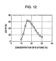
- Fig. 12 shows the rate of resistance change (ΔR/R) as a function of the composition ratio Y of B in CoFeB constituting a second pinned magnetic sublayer in a layered body composed of an underlying layer; Ta (30)/seed layer; Ru (40)/antiferromagnetic layer; IrMn (70)/pinned magnetic layer [first pinned magnetic sublayer; Co70at%Fe30at% (22)/nonmagnetic intermediate sublayer; Ru (9.1)/second pinned magnetic sublayer; (Co50%Fe50%)100-YBY (20)]/insulating barrier layer; Mg-O (11)/free magnetic layer [enhance sublayer; Co50at%Fe50at% (10)/soft magnetic sublayer; Ni87at%Fe13at% (50) ]/protective layer [Ru (20)/Ta (180)] laminated in that order from the bottom. The figures in parentheses are average film thicknesses expressed in angstrom. In this experiment, the layered body was annealed at 270°C for 3.5 hours.
- As shown in Fig. 12, when the composition ratio Y of B was approximately in the range of 15 to 20 atomic percent, the rate of resistance change (ΔR/R) could be increased, but was still low. In addition, as shown in Fig. 12, the rate of resistance change (ΔR/R) changed greatly with the composition ratio Y of B. Thus, a high rate of resistance change (ΔR/R) could not consistently be achieved. Although a large composition ratio Y of B promotes amorphization in a non-heat-treated (as deposited) state, a high rate of resistance change (ΔR/R) is not achieved, as shown in Fig. 12, indicating that crystallization does not proceed by heat treatment.
-
Japanese Unexamined Patent Application Publication No. 2004-179667 - Furthermore, the tunnel magnetoresistive sensor described in
Japanese Unexamined Patent Application Publication No. 2005-197764 - Thus, both of the patent documents do not relate to a tunnel magnetoresistive sensor including an insulating barrier layer formed of Mg-O. In these patent documents, the composition or the structure of a free magnetic layer or a pinned magnetic layer is optimized to improve the characteristics of a tunnel magnetoresistive sensor. Thus, the patent documents do not describe the optimization of the crystal structure of an insulating barrier layer, a free magnetic layer, or a pinned magnetic layer to increase the rate of resistance change (ΔR/R) of the tunnel magnetoresistive sensor.
- Accordingly, the present invention aims to solve the problems described above and, in particular, relates to a tunnel magnetoresistive sensor including an insulating barrier layer formed of Mg-O. The present invention provides a tunnel magnetoresistive sensor that can achieve a high rate of resistance change (ΔR/R) by optimizing the crystal structure of the insulating barrier layer and a method for manufacturing the tunnel magnetoresistive sensor.
- In a tunnel magnetoresistive sensor according to the present invention, a pinned magnetic layer having fixed magnetization, an insulating barrier layer, and a free magnetic layer having variable magnetization according to an external magnetic field are laminated in that order from the bottom, or the free magnetic layer, the insulating barrier layer, and the pinned magnetic layer are laminated in that order from the bottom,
the insulating barrier layer is formed of Mg-O, and
a barrier-layer-side magnetic sublayer constituting at least part of the pinned magnetic layer and being in contact with the insulating barrier layer includes a first magnetic region formed of CoFeB or FeB and a second magnetic region formed of CoFe or Fe, the second magnetic region being disposed between the first magnetic region and the insulating barrier layer. - In the present invention, the first magnetic region preferably includes a composition modulation region in which the concentration of B decreases gradually from a first boundary of the first magnetic region toward the second magnetic region, the first boundary being opposite a second boundary between the first magnetic region and the second magnetic region.
- In the present invention, the barrier-layer-side magnetic sublayer is preferably formed by element diffusion at an interface between a first magnetic subsublayer formed of CoFeB or FeB and a second magnetic subsublayer formed of CoFe or Fe, the second magnetic subsublayer being disposed between the first magnetic subsublayer and the insulating barrier layer, in a layered structure including the first magnetic subsublayer and the second magnetic subsublayer.
- In a tunnel magnetoresistive sensor according to the present invention,
a pinned magnetic layer having fixed magnetization, an insulating barrier layer, and a free magnetic layer having variable magnetization according to an external magnetic field are laminated in that order from the bottom, or the free magnetic layer, the insulating barrier layer, and the pinned magnetic layer are laminated in that order from the bottom,
the insulating barrier layer is formed of Mg-O, and
a barrier-layer-side magnetic sublayer constituting at least part of the pinned magnetic layer and being in contact with the insulating barrier layer has a layered structure including a first magnetic subsublayer formed of CoFeB or FeB and a second magnetic subsublayer formed of CoFe or Fe, the second magnetic subsublayer being disposed between the first magnetic subsublayer and the insulating barrier layer. - In the present invention, a tunnel magnetoresistive sensor including an insulating barrier layer formed of Mg-O was found to achieve a higher rate of resistance change (ΔR/R) than a conventional example in which a pinned magnetic layer is formed of a CoFeB monolayer.
- In the present invention, the first magnetic subsublayer is preferably formed of (CoXFe100-X)100-YBY, wherein the composition ratio Y of B is in the range of 15 to 30 atomic percent.
- In the present invention, the average thickness of the first magnetic subsublayer is preferably in the range of 10 to 30 angstroms.
- In the present invention, the second magnetic subsublayer is preferably formed of CoZFe100-Z, wherein the composition ratio Z of Co is in the range of 0 to 80 atomic percent.
- In the present invention, the average thickness of the second magnetic subsublayer is preferably in the range of 6 to 12 angstroms.
- This can effectively achieve a high rate of resistance change (ΔR/R).
- In the present invention, the barrier-layer-side magnetic sublayer, the insulating barrier layer, and at least a portion of the free magnetic layer in contact with the insulating barrier layer preferably have equivalent crystal faces of a body-centered cubic structure represented by a {100} plane preferentially oriented parallel to the layers. This can effectively achieve a high rate of resistance change (ΔR/R).
- In the present invention, the pinned magnetic layer preferably has a layered ferri structure including a first pinned magnetic sublayer, a nonmagnetic intermediate sublayer, and a second pinned magnetic sublayer laminated in this order, the second pinned magnetic sublayer being the barrier-layer-side magnetic sublayer in contact with the insulating barrier layer.
- In the present invention, the free magnetic layer preferably includes an enhance sublayer and a soft magnetic sublayer disposed on the enhance sublayer, the enhance sublayer being in contact with the insulating barrier layer and being formed of CoFe, the soft magnetic sublayer being formed of a NiFe alloy.
- According to the present invention, a method for manufacturing a tunnel magnetoresistive sensor including a layered portion, the layered portion including a pinned magnetic layer having a fixed magnetization direction, an insulating barrier layer, and a free magnetic layer having a variable magnetization direction according to an external magnetic field laminated in that order from the bottom, includes the steps of:
- (a) stacking a second magnetic subsublayer formed of CoFe or Fe on a first magnetic subsublayer formed of CoFeB or FeB to form a barrier-layer-side magnetic sublayer constituting at least part of the pinned magnetic layer;
- (b) forming an insulating barrier layer formed of Mg-O on the barrier-layer-side magnetic sublayer; and
- (c) forming the free magnetic layer on the insulating barrier layer.
- Alternatively, in the present invention, a method for manufacturing a tunnel magnetoresistive sensor including a layered portion, the layered portion including a free magnetic layer having a variable magnetization direction according to an external magnetic field, an insulating barrier layer, and a pinned magnetic layer having a fixed magnetization direction laminated in that order from the bottom, includes the steps of:
- (d) forming the free magnetic layer;
- (e) forming an insulating barrier layer formed of Mg-O on the free magnetic layer; and
- (f) stacking a second magnetic subsublayer formed of CoFe or Fe and a first magnetic subsublayer formed of CoFeB or FeB on the insulating barrier layer to form a barrier-layer-side magnetic sublayer constituting at least part of the pinned magnetic layer.
- A tunnel magnetoresistive sensor including an insulating barrier layer formed of Mg-O according to the present invention can be manufactured easily and appropriately by the manufacturing method described above. The tunnel magnetoresistive sensor can achieve a higher rate of resistance change (ΔR/R) than before.
- In the present invention, in the formation of the first magnetic subsublayer, the first magnetic subsublayer is preferably formed of (CoXFe100-X)100-YBY, wherein the composition ratio Y of B is controlled within the range of 15 to 30 atomic percent.
- In the present invention, the first magnetic subsublayer preferably has an average thickness in the range of 10 to 30 angstroms.
- In the present invention, in the formation of the second magnetic subsublayer, the second magnetic subsublayer is preferably formed of CoZFe100-Z, wherein the composition ratio Z of Co is controlled within the range of 0 to 80 atomic percent.
- In the present invention, the second magnetic subsublayer preferably has an average thickness in the range of 6 to 12 angstroms.
- This can effectively increase the rate of resistance change (ΔR/R).
- Furthermore, in the present invention, in the formation of the insulating barrier layer, preferably, a Mg layer is formed and is then oxidized to form the insulating barrier layer formed of Mg-O. Alternatively, the insulating barrier layer formed of Mg-O is preferably formed using a Mg-O target.
- In the present invention, annealing is preferably performed after the formation of the layered portion. Depending on the annealing conditions, element diffusion may occur in the barrier-layer-side magnetic sublayer, thus forming a composition modulation region with respect to the concentration of B.
- In the present invention, a tunnel magnetoresistive sensor including an insulating barrier layer formed of Mg-O can achieve a high rate of resistance change (ΔR/R).
-
- Fig. 1 is a cross-sectional view of a tunnel magnetoresistive sensor according to an embodiment of the present invention, taken parallel to a plane of a recording medium;
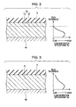
- Fig. 2 is a fragmentary enlarged cross-sectional view of the vicinity of a second pinned
magnetic sublayer 4c illustrated in Fig. 1, particularly illustrating element diffusion at an interface between a first magnetic subsublayer and a second magnetic subsublayer, and a graph illustrating composition modulation with respect to the concentration of B; - Fig. 3 is a fragmentary enlarged cross-sectional view of the vicinity of a second pinned
magnetic sublayer 4c according to another embodiment of the present invention, and a graph illustrating composition modulation with respect to the concentration of B; - Fig. 4 is a process drawing of a method for manufacturing a tunnel magnetoresistive sensor according to an embodiment of the present invention (a cross-sectional view of the tunnel magnetoresistive sensor in a manufacturing process, taken parallel to a plane of a recording medium);
- Fig. 5 is a process drawing following Fig. 4 (a cross-sectional view of the tunnel magnetoresistive sensor in a manufacturing process, taken parallel to a plane of a recording medium);
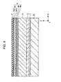
- Fig. 6 is a process drawing following Fig. 5 (a cross-sectional view of the tunnel magnetoresistive sensor in a manufacturing process, taken parallel to a plane of a recording medium);
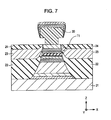
- Fig. 7 is a process drawing following Fig. 6 (a cross-sectional view of the tunnel magnetoresistive sensor in a manufacturing process, taken parallel to a plane of a recording medium);
- Fig. 8 is a graph illustrating the relationship between RA and the rate of resistance change (ΔR/R) in tunnel magnetoresistive sensors including a second pinned magnetic sublayer having a two-layered structure composed of a first magnetic subsublayer and a second magnetic subsublayer and a tunnel magnetoresistive sensor including a second pinned magnetic sublayer having a monolayer structure of a first magnetic subsublayer;
- Fig. 9 is a graph illustrating the relationship between the thickness of a first magnetic subsublayer and the rate of resistance change (ΔR/R) in tunnel magnetoresistive sensors including a second pinned magnetic sublayer having a two-layered structure composed of the first magnetic subsublayer and a second magnetic subsublayer;
- Fig. 10 is a graph illustrating the relationship between the thickness of a second magnetic subsublayer and the rate of resistance change (ΔR/R) in tunnel magnetoresistive sensors including a second pinned magnetic sublayer having a two-layered structure composed of a first magnetic subsublayer and the second magnetic subsublayer;
- Fig. 11 is a graph illustrating the relationship between the thickness of a second magnetic subsublayer and the interlayer coupling magnetic field (Hin) in tunnel magnetoresistive sensors including a second pinned magnetic sublayer having a two-layered structure composed of a first magnetic subsublayer and the second magnetic subsublayer; and
- Fig. 12 is a graph illustrating the relationship between the composition of B of a second pinned magnetic sublayer (first magnetic subsublayer) and the rate of resistance change (ΔR/R) in a tunnel magnetoresistive sensor having a known structure.
- Fig. 1 is a cross-sectional view of a tunnel magnetoresistive sensor (tunnel magnetoresistance effect device) according to the present embodiment, taken parallel to a plane of a recording medium.
- For example, a tunnel magnetoresistive sensor is installed on a trailing edge of a flying slider in a hard disk drive and detects a recording magnetic field of a hard disk. A tunnel magnetoresistive sensor is also used in a magnetoresistive random access memory (MRAM).
- In Fig. 1, the X direction is a track width direction. The Y direction is a direction of a leakage field from a magnetic recording medium (height direction). The Z direction is a direction of movement of a magnetic recording medium such as a hard disk and a lamination direction of the tunnel magnetoresistive sensor.
- The bottom layer in Fig. 1 is a
first shielding layer 21, for example, formed of a NiFe alloy. The layered body T1 is formed on thefirst shielding layer 21. The tunnel magnetoresistive sensor is composed of the layered body T1, first insulatinglayers 22 formed on both sides of the layered body T1 in the track width direction (X direction in Fig. 1), hard bias layers 23, and second insulating layers 24. - The bottom layer of the layered body T1 is an
underlying layer 1 formed of a nonmagnetic material composed of at least one element selected from the group consisting of Ta, Hf, Nb, Zr, Ti, Mo, and W. - A
seed layer 2 is formed on theunderlying layer 1. The seed layer 2.may be formed of Ru or NiFeCr. Theseed layer 2 formed of NiFeCr has equivalent crystal faces of a face-centered cubic (fcc) structure represented by a {111} plane preferentially oriented parallel to theseed layer 2. Theseed layer 2 formed of Ru has equivalent crystal faces of a hexagonal closest packed (hcp) structure represented by a {000} plane preferentially oriented parallel to theseed layer 2. Theunderlying layer 1 may be eliminated. - An
antiferromagnetic layer 3 formed on theseed layer 2 is preferably formed of an antiferromagnetic material containing an element α (wherein α is one or at least two elements selected from the group consisting of Pt, Pd, Ir, Rh, Ru, and Os) and Mn. - α-Mn alloys containing an element of the platinum group have excellent characteristics as antiferromagnetic materials, such as high corrosion resistance and high blocking temperature. Furthermore, the α-Mn alloys can have an increased exchange coupling magnetic field (Hex).
- Alternatively, the
antiferromagnetic layer 3 may be formed of an antiferromagnetic material containing an element α, an element α' (wherein the element α' is at least one element selected from the group consisting of Ne, Ar, Kr, Xe, Be, B, C, N, Mg, Al, Si, P, Ti, V, Cr, Fe, Co, Ni, Cu, Zn, Ga, Ge, Zr, Nb, Mo, Ag, Cd, Sn, Hf, Ta, W, Re, Au, Pb, and rare earth elements), and Mn. - A pinned
magnetic layer 4 is formed on theantiferromagnetic layer 3. The pinnedmagnetic layer 4 has a layered ferri structure including a first pinnedmagnetic sublayer 4a, a nonmagneticintermediate sublayer 4b, and a second pinned magnetic sublayer (barrier-layer-side magnetic sublayer) 4c laminated in that order from the bottom. The directions of magnetization of the first pinnedmagnetic sublayer 4a and the second pinnedmagnetic sublayer 4c are brought into an antiparallel state by an exchange coupling magnetic field at an interface between theantiferromagnetic layer 3 and the pinnedmagnetic layer 4 and an antiferromagnetic exchange coupling magnetic field via the nonmagneticintermediate sublayer 4b (RKKY interaction). This is a so-called layered ferri structure. This structure can stabilize the magnetization of the pinnedmagnetic layer 4 and apparently increase an exchange coupling magnetic field generated at the interface between the pinnedmagnetic layer 4 and theantiferromagnetic layer 3. For example, the first pinnedmagnetic sublayer 4a has a thickness in the range of 1.2 to 3.2 nm (12 to 32 angstroms), the nonmagneticintermediate sublayer 4b has a thickness approximately in the range of 0.8 to 1 nm (8 to 10 angstroms), and the second pinnedmagnetic sublayer 4c has a thickness in the range of 1.6 to 4.2 nm (16 to 42 angstaoms). - The first pinned
magnetic sublayer 4a is formed of a ferromagnetic material such as CoFe, NiFe, or CoFeNi. The nonmagneticintermediate sublayer 4b is formed of a nonmagnetic conductive material such as Ru, Rh, Ir, Cr, Re, or Cu. - In the present embodiment, the second pinned
magnetic sublayer 4c is composed of a first magnetic subsublayer 4cl formed of CoFeB or FeB and a second magnetic subsublayer 4c2 formed of CoFe or Fe. - An insulating
barrier layer 5 formed on the pinnedmagnetic layer 4 is formed of magnesium oxide (Mg-O). The insulatingbarrier layer 5 has a thickness approximately in the range of 0.6 to 1.2 nm. Mg-O preferably contains 40 to 60 atomic percent of Mg and is most preferably Mg50at%O50at%. - Furthermore, a Mg layer having a very small thickness (for example, 1 to 6 angstroms) may be formed between the insulating
barrier layer 5 and the second pinnedmagnetic sublayer 4c. - A free
magnetic layer 6 is formed on the insulatingbarrier layer 5. The freemagnetic layer 6 is composed of a softmagnetic sublayer 6b formed of a magnetic material such as a NiFe alloy and an enhancesublayer 6a formed of a CoFe alloy. The enhancesublayer 6a is disposed between the softmagnetic sublayer 6b and the insulatingbarrier layer 5. Preferably, the softmagnetic sublayer 6b is formed of a magnetic material having excellent soft magnetism. The enhancesublayer 6a is formed of a magnetic material having spin polarizability larger than that of the softmagnetic sublayer 6b. The enhancesublayer 6a formed of a CoFe alloy having large spin polarizability can improve the rate of resistance change (ΔR/R). - The free
magnetic layer 6 may be a layered ferri structure in which a plurality of magnetic sublayers is laminated with nonmagnetic intermediate sublayers. The width of the freemagnetic layer 6 in the track width direction (X direction in Fig. 1) defines the track width Tw. - A
protective layer 7, for example, formed of Ta is formed on the freemagnetic layer 6. - End faces 12 on both sides of the layered body T1 in the track width direction (X direction in Fig. 1) have inclined faces formed such that the width of the layered body T1 in the track width direction decreases gradually from the bottom to the top.
- As illustrated in Fig. 1, the first insulating
layers 22 disposed on both sides of the layered body T1 are formed on thefirst shielding layer 21 along the end faces 12 of the layered body T1. The hard bias layers 23 are formed on the first insulating layers 22. The second insulatinglayers 24 are formed on the hard bias layers 23. - Bias underlying layers (not shown) may be formed between the first insulating
layers 22 and the hard bias layers 23. The bias underlying layers may be formed of Cr, W, and/or Ti. - The first insulating
layers 22 and the second insulatinglayers 24 are formed of an insulating material such as Al2O3 or SiO2. The first insulatinglayers 22 and the second insulatinglayers 24 insulate the hard bias layers 23 to prevent an electric current flowing through the layered body T1 in a direction perpendicular to the interfaces of the layers of the layered body T1 from being shunted to both sides of the layered body T1 in the track width direction. For example, the hard bias layers 23 are formed of a Co-Pt (cobalt-platinum) alloy or a Co-Cr-Pt (cobalt-chromium-platinum) alloy. - A
second shielding layer 26, for example, formed of a NiFe alloy is formed on the layered body T1 and the second insulating layers 24. - In the embodiment illustrated in Fig. 1, the
first shielding layer 21 and thesecond shielding layer 26 function as electrode layers of the layered body T1. Thus, an electric current flows in a direction perpendicular to the layers of the layered body T1 (in a direction parallel to the Z direction in Fig. 1). - The free
magnetic layer 6 is magnetized in a direction parallel to the track width direction (X direction in Fig. 1) under the influence of a bias magnetic field of the hard bias layers 23. The first pinnedmagnetic sublayer 4a and the second pinnedmagnetic sublayer 4c together constituting the pinnedmagnetic layer 4 are magnetized in a direction parallel to the height direction (Y direction in Fig. 1). Because the pinnedmagnetic layer 4 has a layered ferri structure, the magnetization of the first pinnedmagnetic sublayer 4a is antiparallel to the magnetization of the second pinnedmagnetic sublayer 4c. While the magnetization of the pinnedmagnetic layer 4 is fixed (an external magnetic field does not change the magnetization), the magnetization of the freemagnetic layer 6 changes with the external magnetic field. - When the magnetization of the second pinned
magnetic sublayer 4c is antiparallel to the magnetization of the freemagnetic layer 6, a change in the magnetization of the freemagnetic layer 6 caused by an external magnetic field reduces a tunneling current flowing through the insulatingbarrier layer 5 disposed between the second pinnedmagnetic sublayer 4c and the freemagnetic layer 6, thus maximizing the resistance. On the other hand, when the magnetization of the second pinnedmagnetic sublayer 4c is parallel to the magnetization of the freemagnetic layer 6, a change in the magnetization of the freemagnetic layer 6 caused by an external magnetic field maximizes the tunneling current, thus minimizing the resistance. - According to this principle, an external magnetic field changes the magnetization of the free
magnetic layer 6 and thereby changes the electrical resistance. The tunnel magnetoresistive sensor detects the change in electrical resistance as a voltage change and thereby detects a leakage field from a recording medium. - The features of the embodiment illustrated in Fig. 1 will be described below.
- In Fig. 1, the insulating
barrier layer 5 is formed of magnesium oxide (Mg-O). The second pinnedmagnetic sublayer 4c constituting the pinnedmagnetic layer 4 underlying the insulatingbarrier layer 5 is formed in contact with the insulatingbarrier layer 5. The second pinnedmagnetic sublayer 4c is composed of the first magnetic subsublayer 4cl formed of CoFeB or FeB and the second magnetic subsublayer 4c2 formed of CoFe or Fe. The second magnetic subsublayer 4c2 is disposed between the first magnetic subsublayer 4c1 and the insulatingbarrier layer 5. - Experiments described below show that this structure can achieve a higher rate of resistance change (ΔR/R) than a conventional example in which the second pinned
magnetic sublayer 4c is formed of a CoFeB monolayer. Thus, a tunnel magnetoresistive sensor can have a high head output even at a narrower track. - As in the present embodiment, when the first magnetic subsublayer 4c1 formed of CoFeB or FeB having a tendency of becoming amorphous is formed on the nonmagnetic
intermediate sublayer 4b in a non-heat-treated (as deposited) state, the first magnetic subsublayer 4c1 may block the influence of the crystalline orientation exerted by the crystal structures of from theseed layer 2 to the nonmagneticintermediate sublayer 4b (for example, the orientation of a face-centered cubic structure {111} plane). Hence, the crystal structures of the second magnetic subsublayer 4c2, the insulatingbarrier layer 5, and the freemagnetic layer 6 formed on the first magnetic subsublayer 4c1 may be less affected by the crystalline orientation of the crystal structures of from theseed layer 2 to the nonmagneticintermediate sublayer 4b. In the present embodiment, since the second magnetic subsublayer 4c2 formed of CoFe or Fe, which is easy to crystallize, is formed on the first magnetic subsublayer 4c1, preferred orientation of equivalent crystal faces of a body-centered cubic (bcc) structure represented by a {100} plane tends to occur in the second pinnedmagnetic sublayer 4c, the insulatingbarrier layer 5, and the enhancesublayer 6a formed of CoFe after heat treatment. The phrase "crystal faces represented by a {100} plane" refers to crystal faces expressed by Miller indices. The equivalent crystal faces represented by a {100} plane include a (100) plane, a (-100) plane, a (010) plane a (0-10) plane, a (001) plane, and a (00-1) plane. - Thus, the present embodiment can achieve a higher rate of resistance change (ΔR/R) than before.
- In the present embodiment, the thickness of the first magnetic subsublayer 4c1 is preferably in the range of 10 to 30 angstroms and is more preferably in the range of 16 to 24 angstroms. According to an experiment described below, a change in the thickness of the first magnetic subsublayer 4c1 does not cause a large change in the rate of resistance change (ΔR/R). However, because an increased thickness of the first magnetic subsublayer 4c1 results in an increase in the B content in the entire second pinned
magnetic sublayer 4c, it will have an influence on the crystallization of the second magnetic subsublayer 4c2 formed on the first magnetic subsublayer 4c1. Hence, the thickness of the first magnetic subsublayer 4c1 is preferably in the range described above. - Furthermore, the thickness of the second magnetic subsublayer 4c2 is preferably in the range of 6 to 12 angstroms and is more preferably in the range of 7 to 11 angstroms. According to an experiment described below, when the thickness of the second magnetic subsublayer is smaller than 6 angstroms or larger than 12 angstroms, the rate of resistance change (ΔR/R) is not increased. In contrast, when the thickness of a second magnetic subsublayer 4c2 is in the range of 7 to 11 angstroms, a high rate of resistance change (ΔR/R) is achieved consistently. According to another experiment described below, the thickness of the second magnetic subsublayer 4c2 in the range described above can reduce the interlayer coupling magnetic field (Hin) between the free
magnetic layer 6 and the pinnedmagnetic layer 4. Furthermore, in terms of the interlayer coupling magnetic field (Hin), the thickness of the second magnetic subsublayer 4c2 is preferably as large as possible within the range described above. - In the present embodiment, the first magnetic subsublayer 4c1 is preferably formed of (CoXFe100-X)100-YBY, wherein the composition ratio Y of B is in the range of 15 to 30 atomic percent. The composition of the first magnetic subsublayer 4c1 can be controlled within the range described above to achieve a high rate of resistance change (ΔR/R).
- Furthermore, the atomic ratio X {composition ratio of Co/(composition ratio of Co + composition ratio of Fe)} is preferably in the range of 0% to 80%.
- The second magnetic subsublayer 4c2 is preferably formed of CoZFe100-Z, wherein the composition ratio Z of Co is in the range of 0 to 80 atomic percent. More preferably, the composition ratio Z of Co is in the range of 10 to 50 atomic percent.
- As described below, a tunnel magnetoresistive sensor is subjected to annealing (heat treatment) in a manufacturing process. For example, annealing is performed at a temperature approximately in the range of 200°C to 310°C. Annealing may be performed in a magnetic field to generate an exchange coupling magnetic field (Hex) between the first pinned
magnetic sublayer 4a constituting the pinnedmagnetic layer 4 and theantiferromagnetic layer 3. - For example, when the annealing temperature is lower than 200°C, no interdiffusion of a component element may occur at an interface between the second magnetic subsublayer 4c2 and the first magnetic subsublayer 4c1, or, if any, the interdiffusion of a component element may occur on a small scale (for example, the interdiffusion does not occur over the entire interface but occurs intermittently). Thus, the state of the interface may be almost maintained.
- On the other hand, when the annealing temperature is in the range of 200°C to 310°C and the annealing time is at least four hours, the interdiffusion of a component element may occur at an interface between the second magnetic subsublayer 4c2 and the first magnetic subsublayer 4c1, as illustrated in Fig. 2 or 3. The interdiffusion of a component element can eliminate the interface and form a composition modulation region with respect to the concentration of B.
- In an embodiment illustrated in Fig. 2, element diffusion occurs at an interface between the second magnetic subsublayer 4c2 and the first magnetic subsublayer 4c1. The second pinned
magnetic sublayer 4c is composed of a firstmagnetic region 10 formed of CoFeB or FeB and a secondmagnetic region 11 formed of CoFe or Fe. The secondmagnetic region 11 is disposed between the firstmagnetic region 10 and the insulatingbarrier layer 5. - As shown in Fig. 2, the second
magnetic region 11 is free of B. As shown in an inset in Fig. 2, the firstmagnetic region 10 includes a composition modulation region in which the concentration of B decreases gradually from an undersurface (interface in contact with the nonmagneticintermediate sublayer 4b) toward the secondmagnetic region 11. The concentration of B in the vicinity of the undersurface of the firstmagnetic region 10 is lower than that in the inside of the firstmagnetic region 10. This results from element diffusion between the firstmagnetic region 10 and the nonmagneticintermediate sublayer 4b. - On the other hand, in an embodiment illustrated in Fig. 3, the second pinned
magnetic sublayer 4c is entirely formed of CoFeB. The concentration of B is lower in the top surface side in contact with the insulatingbarrier layer 5 than in the undersurface side in contact with the nonmagneticintermediate sublayer 4b. As shown in Fig. 3, the second pinnedmagnetic sublayer 4c includes a composition modulation region in which the concentration of B decreases gradually from the undersurface side in contact with the nonmagneticintermediate sublayer 4b to the top surface side in contact with the insulatingbarrier layer 5. Furthermore, as shown in Fig. 3, the concentration of B in the vicinity of the undersurface of the second pinnedmagnetic sublayer 4c is lower than that in the inside of the second pinnedmagnetic sublayer 4c. This results from element diffusion between the second pinnedmagnetic sublayer 4c and the nonmagneticintermediate sublayer 4b. - In the embodiment illustrated in Fig. 1, the pinned
magnetic layer 4 has a layered ferri structure composed of the first pinnedmagnetic sublayer 4a, the nonmagneticintermediate sublayer 4b, and the second pinnedmagnetic sublayer 4c. However, the present embodiment can be applied to the pinnedmagnetic layer 4 having a monolayer structure or a layered structure composed of a plurality of magnetic layers. In the pinnedmagnetic layer 4 having a layered ferri structure, the magnetization of the pinnedmagnetic layer 4 can be fixed more appropriately. The pinnedmagnetic layer 4 having a layered ferri structure is therefore suitable to improve the playback output. - The embodiment illustrated in Fig. 1 is a so-called bottom-type tunnel magnetoresistive sensor, in which the insulating
barrier layer 5 is formed on the pinnedmagnetic layer 4. The present embodiment can also be applied to a so-called top-type layered structure, in which the pinnedmagnetic layer 4 is formed on the insulatingbarrier layer 5. In the top-type layered structure, the freemagnetic layer 6, the insulatingbarrier layer 5, the pinnedmagnetic layer 4, and theantiferromagnetic layer 3 are laminated in that order from the bottom. The second pinnedmagnetic sublayer 4c constituting the pinnedmagnetic layer 4 is composed of the second magnetic subsublayer 4c2 formed of CoFe or Fe and the first magnetic subsublayer 4c1 formed of CoFeB or FeB laminated in that order from the bottom. Element diffusion may occur between the second magnetic subsublayer 4c2 and the first magnetic subsublayer 4cl. - The present embodiment can also be applied to a dual-type tunnel magnetoresistive sensor composed of a first antiferromagnetic layer, a first pinned magnetic layer, a first insulating barrier layer, a free magnetic layer, a second insulating barrier layer, a second pinned magnetic layer, and a second antiferromagnetic layer laminated in that order from the bottom. The structure of the first pinned magnetic layer is described in Figs. 1 to 3. The structure of the second pinned magnetic layer is described for the top-type layered structure.
- A method for manufacturing a tunnel magnetoresistive sensor according to the present embodiment will be described below. Figs. 4 to 7 are fragmentary sectional views of a tunnel magnetoresistive sensor in a manufacturing process, taken in the same direction as in Fig. 1.
- In a process illustrated in Fig. 4, an
underlying layer 1, aseed layer 2, anantiferromagnetic layer 3, a first pinnedmagnetic sublayer 4a, a nonmagneticintermediate sublayer 4b, and a second pinnedmagnetic sublayer 4c are successively formed on afirst shielding layer 21. These layers may be deposited by sputtering. - In the present embodiment, as illustrated in Fig. 2, the second pinned
magnetic sublayer 4c is composed of a first magnetic subsublayer 4c1 formed of CoFeB or FeB and a second magnetic subsublayer 4c2 formed of CoFe or Fe laminated in that order from the bottom. - The first magnetic subsublayer 4c1 is preferably formed of (CoXFe100-X)100-YBY, wherein the composition ratio Y of B is in the range of 15 to 30 atomic percent, and the atomic ratio X is in the range of 0% to 80%. Furthermore, the first magnetic subsublayer 4c1 preferably has an average thickness in the range of 10 to 30 angstroms. This can achieve a high rate of resistance change (ΔR/R).
- Furthermore, the second magnetic subsublayer 4c2 is preferably formed of CoZFe100-Z, wherein the composition ratio Z of Co is controlled within the range of 0 to 80 atomic percent. Furthermore, the second magnetic subsublayer 4c2 preferably has an average thickness in the range of 6 to 12 angstroms. This can achieve a high rate of resistance change (ΔR/R).
- The surface of the second pinned
magnetic sublayer 4c is then subjected to plasma processing. The plasma processing is performed to improve the flatness of the surface of the second pinnedmagnetic sublayer 4c. As in the present embodiment, in a structure in which a thin second magnetic subsublayer 4c2 is formed on a sufficiently flat first magnetic subsublayer 4c1, the surface of the second pinnedmagnetic sublayer 4c is also sufficiently flat. The plasma processing may therefore be eliminated. - An insulating
barrier layer 5 formed of Mg-O is then formed on the second pinnedmagnetic sublayer 4c. In the present embodiment, the insulatingbarrier layer 5 formed of Mg-O is directly formed, for example, by RF sputtering, using a Mg-O target. - Alternatively, a Mg layer may be formed on the second pinned
magnetic sublayer 4c by sputtering, and the Mg layer may be oxidized to form the insulatingbarrier layer 5 formed of Mg-O. Examples of the oxidizing method include radical oxidation, ion oxidation, plasma oxidation, and natural oxidation. The Mg layer has a thickness approximately in the range of 2 to 10 angstroms. - In a process illustrated in Fig. 5, a free
magnetic layer 6 composed of an enhancesublayer 6a and a softmagnetic sublayer 6b, and aprotective layer 7 are formed on the insulatingbarrier layer 5. - In the present embodiment, the enhance
sublayer 6a is preferably formed of CoFe in which the Fe composition ratio is in the range of 5 to 90 atomic percent. Furthermore, the softmagnetic sublayer 6b is preferably formed of a NiFe alloy in which the Ni composition ratio is in the range of 78 to 92 atomic percent. - Thus, a layered body T1 including from the
underlying layer 1 to theprotective layer 7 is formed. - A lift-off resist
layer 30 is then formed on the layered body T1. Both ends of the layered body T1 in the track width direction (X direction) that are not covered with the lift-off resistlayer 30 are removed, for example, by etching (see Fig. 6). - First insulating
layers 22, hard bias layers 23, and second insulatinglayers 24 are then stacked on thefirst shielding layer 21 on both sides of the layered body T1 in the track width direction (X direction) in that order from the bottom (see Fig. 7). - The lift-off resist
layer 30 is then removed to form asecond shielding layer 26 on the layered body T1 and the second insulating layers 24. - The method for manufacturing a tunnel magnetoresistive sensor described above includes annealing. Annealing is typically performed to generate an exchange coupling magnetic field (Hex) between the
antiferromagnetic layer 3 and the first pinnedmagnetic sublayer 4a. - When the annealing temperature is lower than 200°C, no interdiffusion of a component element may occur at interfaces between the layers, or, if any, the interdiffusion of a component element may occur on a small scale (for example, the interdiffusion does not occur over the entire interface but occurs intermittently). Thus, the state of the interface may be almost maintained.
- On the other hand, for example, when the annealing temperature is in the range of 200°C to 310°C and the annealing time is at least four hours, the interdiffusion of a component element may occur at interfaces between the layers. The interdiffusion of a component element can eliminate an interface between the first magnetic subsublayer 4c1 and the second magnetic subsublayer 4c2 in the second pinned
magnetic sublayer 4c and form a composition modulation region with respect to the concentration of B. - In the present embodiment, a tunnel magnetoresistive sensor that can achieve a high rate of resistance change (ΔR/R) can easily and appropriately be manufactured by the manufacturing methods described above.
- In particular, the two-layered structure of the second pinned
magnetic sublayer 4c composed of the first magnetic subsublayer 4c1 and the second magnetic subsublayer 4c2 as described above can achieve a higher rate of resistance change (ΔR/R) than a conventional example in which the second pinnedmagnetic sublayer 4c is formed of a CoFeB monolayer. - The manufacturing method according to the present embodiment is a method for manufacturing a so-called bottom-type tunnel magnetoresistive sensor. However, the manufacturing method can be applied to so-called top-type tunnel magnetoresistive sensors or dual-type tunnel magnetoresistive sensors.
- A tunnel magnetoresistive sensor illustrated in Fig. 1 was formed.
- A layered body T1 was composed of an
underlying layer 1; Ta (30)/seed layer 2; Ru (40)/antiferromagnetic layer 3; IrMn (70)/pinned magnetic layer 4 [first pinnedmagnetic sublayer 4a; Co70at%Fe30at% (22)/nonmagneticintermediate sublayer 4b; Ru (9. 1) /second pinnedmagnetic sublayer 4c; (Co50%Fe50%)100-YBY (20)]/insulatingbarrier layer 5; Mg-O (11)/free magnetic layer 6 [enhancesublayer 6a; Co50at%Fe50at% (10)/softmagnetic sublayer 6b; Ni87at%Fe13at% (50)]/protective layer 7 [Ru (20)/Ta (180)] laminated in that order from the bottom. The figures in parentheses are average film thicknesses expressed in angstrom. - The surface of the second pinned
magnetic sublayer 4c was subjected to plasma processing before the formation of the insulatingbarrier layer 5. The insulatingbarrier layer 5 was then formed on the second pinnedmagnetic sublayer 4c by sputtering using a Mg-O target. - In the examples, the layered body was annealed at 270°C for 3.5 hours.
- In the examples, the following structures were formed as the second pinned
magnetic sublayer 4c. - A layered structure composed of (Co50%Fe50%)85at%B15at% (22)/Co50at%Fe50at% (4) laminated in that order from the bottom.
- A layered structure composed of (Co50%Fe50%)77at%B23at% (20)/Co50at%Fe50at% (6) laminated in that order from the bottom.
- A layered structure composed of (Co50%Fe50%)70at%B30at% (18)/Co50at%Fe50at% (8) laminated in that order from the bottom.
- A layered structure composed of (Co50%Fe50%)70at%B30at% (t1)/Co50at%Fe50at% (8) laminated in that order from the bottom, wherein the thickness t1 of a first magnetic subsublayer 4c1 is 16, 18, 20, 22, or 24 angstroms.
- A layered structure composed of (Co50%Fe50%)70at%B30at% (t1)/Co50at%Fe50at% (9) laminated in that order from the bottom, wherein the thickness t1 of a first magnetic subsublayer 4c1 is 16, 18, 20, 22, or 24 angstroms.
- A layered structure composed of (Co50%Fe50%)70at%B30at% (t1)/Co50at%Fe50at% (10) laminated in that order from the bottom, wherein the thickness t1 of a first magnetic subsublayer 4c1 is 16, 18, 20, 22, or 24 angstroms.
- A layered structure composed of (Co50%Fe50%)70at%B30at% (20)/Co50at%Fe50at% (t2) laminated in that order from the bottom, wherein the thickness t2 of a second magnetic subsublayer 4c2 is 6, 7, 8, 9, 10, 11, or 12 angstroms.
- The figures in parentheses in Examples 1 to 12 and Comparative Example 1 are average film thicknesses expressed in angstroms.
- For tunnel magnetoresistive sensors including the second pinned
magnetic sublayers 4c having these structures, the rate of resistance change (ΔR/R), RA (resistance R x area A), and the interlayer coupling magnetic field (Hin) were determined. - Fig. 8 shows the relationship between RA and the rate of resistance change (ΔR/R) in Examples 1 to 3 and Comparative Example 1. In an experiment shown in Fig. 8, RA of each sample of Examples 1 to 3 and Comparative Example 1 was changed by changing the thickness of the insulating
barrier layer 5 formed of Mg-O within the range of 8 to 12 angstroms. - As shown in Fig. 8, Examples 1 to 3, in which the second pinned
magnetic sublayer 4c was a layered structure composed of the first magnetic subsublayer 4c1 and the second magnetic subsublayer 4c2, had a higher rate of resistance change (ΔR/R) than Comparative Example 1, in which the second pinnedmagnetic sublayer 4c was formed only of the first magnetic subsublayer. Furthermore, while Examples 1 to 3 had a little larger RAs than Comparative Example 1, it does not have a large effect on the characteristics of a head. - Fig. 9 shows the relationship between the thickness (t1) of a first magnetic subsublayer 4c1 and the rate of resistance change (ΔR/R) in Examples 4 to 6.
- Fig. 9 shows that, when the thickness of a first magnetic subsublayer 4c1 formed of CoFeB was in the range of 16 to 24 angstroms, the rate of resistance change (ΔR/R) was almost constant.
- Fig. 10 shows the rate of resistance change (ΔR/R) in Examples 7 to 13, in which the thickness (t2) of the second magnetic subsublayer 4c2 was in the range of 6 to 12 angstroms, and Comparative Example 1, in which the second pinned
magnetic sublayer 4c was formed of a CoFeB monolayer (that is, the thickness of the second magnetic subsublayer 4c2 was zero angstroms). - Fig. 10 shows that Examples 7 to 13, in which the thickness of the second magnetic subsublayer 4c2 was in the range of 6 to 12 angstroms, had a higher rate of resistance change (ΔR/R) than Comparative Example 1, in which the thickness of the second magnetic subsublayer 4c2 was zero angstroms. Furthermore, it was found that when the thickness of the second magnetic subsublayer 4c2 was in the range of 7 to 11 angstroms, in particular in the range of 8 to 10 angstroms, a much higher rate of resistance change (ΔR/R) was achieved.
- Fig. 11 shows the interlayer coupling magnetic field (Hin) between the free
magnetic layer 6 and the pinnedmagnetic layer 4 in Examples 7 to 13 and Comparative Example 1. - Fig. 11 shows that when the thickness of the second magnetic subsublayer 4c2 was in the range of 6 to 12 angstroms, the interlayer coupling magnetic field Hin could be larger than that of Comparative Example 1. Thus, it is believed that the flatness of an interface between the pinned magnetic layer and the insulating barrier layer was improved in the present examples relative to Comparative Example 1. Furthermore, as shown in Fig. 11, in the examples, the interlayer coupling magnetic field Hin was found to decrease with increasing average thickness of the second magnetic subsublayer (CoFe layer). Thus, when the average thickness of the second magnetic subsublayer 4c2 is in the range of 6 to 12 angstroms, a larger average thickness within this range will be preferred.
- These experimental results show that the layered structure of the second pinned
magnetic sublayer 4c composed of the first magnetic subsublayer 4c1 and the second magnetic subsublayer 4c2 can achieve a high rate of resistance change (ΔR/R).
Claims (20)
- A tunnel magnetoresistive sensor, wherein
a pinned magnetic layer having fixed magnetization, an insulating barrier layer, and a free magnetic layer having variable magnetization according to an external magnetic field are laminated in that order from the bottom, or the free magnetic layer, the insulating barrier layer, and the pinned magnetic layer are laminated in that order from the bottom,
the insulating barrier layer is formed of Mg-O, and
a barrier-layer-side magnetic sublayer constituting at least part of the pinned magnetic layer and being in contact with the insulating barrier layer includes a first magnetic region formed of CoFeB or FeB and a second magnetic region formed of CoFe or Fe, the second magnetic region being disposed between the first magnetic region and the insulating barrier layer. - The tunnel magnetoresistive sensor according to Claim 1, wherein the first magnetic region includes a composition modulation region in which the concentration of B decreases gradually from a first boundary of the first magnetic region toward the second magnetic region, the first boundary being opposite a second boundary between the first magnetic region and the second magnetic region.
- The tunnel magnetoresistive sensor according to Claim 1 or 2, wherein the barrier-layer-side magnetic sublayer is formed by element diffusion at an interface between a first magnetic subsublayer formed of CoFeB or FeB and a second magnetic subsublayer formed of CoFe or Fe, the second magnetic subsublayer being disposed between the first magnetic subsublayer and the insulating barrier layer, in a layered structure including the first magnetic subsublayer and the second magnetic subsublayer.
- A tunnel magnetoresistive sensor, wherein
a pinned magnetic layer having fixed magnetization, an insulating barrier layer, and a free magnetic layer having variable magnetization according to an external magnetic field are laminated in that order from the bottom, or the free magnetic layer, the insulating barrier layer, and the pinned magnetic layer are laminated in that order from the bottom,
the insulating barrier layer is formed of Mg-O, and
a barrier-layer-side magnetic sublayer constituting at least part of the pinned magnetic layer and being in contact with the insulating barrier layer has a layered structure including a first magnetic subsublayer formed of CoFeB or FeB and a second magnetic subsublayer formed of CoFe or Fe, the second magnetic subsublayer being disposed between the first magnetic subsublayer and the insulating barrier layer. - The tunnel magnetoresistive sensor according to Claim 3 or 4, wherein the first magnetic subsublayer is formed of (CoXFe100-X)100-YBY, wherein the composition ratio Y of B is in the range of 15 to 30 atomic percent.
- The tunnel magnetoresistive sensor according to any of Claims 3 to 5, wherein the average thickness of the first magnetic subsublayer is in the range of 10 to 30 angstroms.
- The tunnel magnetoresistive sensor according to any of Claims 3 to 6, wherein the second magnetic subsublayer is formed of CoZFe100-Z, wherein the composition ratio Z of Co is in the range of 0 to 80 atomic percent.
- The tunnel magnetoresistive sensor according to any of Claims 3 to 7, wherein the average thickness of the second magnetic subsublayer is in the range of 6 to 12 angstroms.
- The tunnel magnetoresistive sensor according to any of Claims 1 to 8, wherein the barrier-layer-side magnetic sublayer, the insulating barrier layer, and at least a portion of the free magnetic layer in contact with the insulating barrier layer have equivalent crystal faces of a body-centered cubic structure represented by a {100} plane preferentially oriented parallel to the layers.
- The tunnel magnetoresistive sensor according to any of Claims 1 to 9, wherein the pinned magnetic layer has a layered ferri structure including a first pinned magnetic sublayer, a nonmagnetic intermediate sublayer, and a second pinned magnetic sublayer laminated in this order, the second pinned magnetic sublayer being the barrier-layer-side magnetic sublayer in contact with the insulating barrier layer.
- The tunnel magnetoresistive sensor according to any of Claims 1 to 10, wherein the free magnetic layer includes an enhance sublayer and a soft magnetic sublayer disposed on the enhance sublayer, the enhance sublayer being in contact with the insulating barrier layer and being formed of CoFe, the soft magnetic sublayer being formed of a NiFe alloy.
- A method for manufacturing a tunnel magnetoresistive sensor including a layered portion, the layered portion including a pinned magnetic layer having a fixed magnetization direction, an insulating barrier layer, and a free magnetic layer having a variable magnetization direction according to an external magnetic field laminated in that order from the bottom, the method comprising the steps of:(a) stacking a second magnetic subsublayer formed of CoFe or Fe on a first magnetic subsublayer formed of CoFeB or FeB to form a barrier-layer-side magnetic sublayer constituting at least part of the pinned magnetic layer;(b) forming an insulating barrier layer formed of Mg-O on the barrier-layer-side magnetic sublayer; and(c) forming the free magnetic layer on the insulating barrier layer.
- A method for manufacturing a tunnel magnetoresistive sensor including a layered portion, the layered portion including a free magnetic layer having a variable magnetization direction according to an external magnetic field, an insulating barrier layer, and a pinned magnetic layer having a fixed magnetization direction laminated in that order from the bottom, the method comprising the steps of:(d) forming the free magnetic layer;(e) forming an insulating barrier layer formed of Mg-O on the free magnetic layer; and(f) stacking a second magnetic subsublayer formed of CoFe or Fe and a first magnetic subsublayer formed of CoFeB or FeB on the insulating barrier layer to form a barrier-layer-side magnetic sublayer constituting at least part of the pinned magnetic layer.
- The method for manufacturing a tunnel magnetoresistive sensor according to Claim 12 or 13, wherein, in the formation of the first magnetic subsublayer, the first magnetic subsublayer is formed of (CoXFe100-X)100-YBY, wherein the composition ratio Y of B is controlled within the range of 15 to 30 atomic percent.
- The method for manufacturing a tunnel magnetoresistive sensor according to any of Claims 12 to 14, wherein the first magnetic subsublayer has an average thickness in the range of 10 to 30 angstroms.
- The method for manufacturing a tunnel magnetoresistive sensor according to any of Claims 12 to 15, wherein, in the formation of the second magnetic subsublayer, the second magnetic subsublayer is formed of CoZFe100-Z, wherein the composition ratio Z of Co is controlled within the range of 0 to 80 atomic percent.
- The method for manufacturing a tunnel magnetoresistive sensor according to any of Claims 12 to 16, wherein the second magnetic subsublayer has an average thickness in the range of 6 to 12 angstroms.
- The method for manufacturing a tunnel magnetoresistive sensor according to any of Claims 12 to 17, wherein, in the formation of the insulating barrier layer, a Mg layer is formed and is then oxidized to form the insulating barrier layer formed of Mg-O.
- The method for manufacturing a tunnel magnetoresistive sensor according to any of Claims 12 to 18, wherein, in the formation of the insulating barrier layer, the insulating barrier layer formed of Mg-O is formed using a Mg-O target.
- The method for manufacturing a tunnel magnetoresistive sensor according to any of Claims 12 to 19, wherein annealing is performed after the formation of the layered portion.
Applications Claiming Priority (2)
| Application Number | Priority Date | Filing Date | Title |
|---|---|---|---|
| JP2006255646 | 2006-09-21 | ||
| JP2007065628A JP5210533B2 (en) | 2006-09-21 | 2007-03-14 | Tunnel-type magnetic sensing element and manufacturing method thereof |
Publications (3)
| Publication Number | Publication Date |
|---|---|
| EP1903624A2 true EP1903624A2 (en) | 2008-03-26 |
| EP1903624A3 EP1903624A3 (en) | 2011-08-31 |
| EP1903624B1 EP1903624B1 (en) | 2012-07-25 |
Family
ID=38896956
Family Applications (1)
| Application Number | Title | Priority Date | Filing Date |
|---|---|---|---|
| EP07018080A Not-in-force EP1903624B1 (en) | 2006-09-21 | 2007-09-14 | Tunnel magnetoresistive sensor in which at least part of pinned layer is composed of CoFeB layer and method for manufacturing the tunnel magnetoresistive sensor |
Country Status (3)
| Country | Link |
|---|---|
| US (1) | US7969693B2 (en) |
| EP (1) | EP1903624B1 (en) |
| JP (1) | JP5210533B2 (en) |
Cited By (8)
| Publication number | Priority date | Publication date | Assignee | Title |
|---|---|---|---|---|
| US20080070063A1 (en) * | 2006-09-15 | 2008-03-20 | Fujitsu Limited | Exchange coupling film and magnetic device |
| WO2010037075A1 (en) * | 2008-09-29 | 2010-04-01 | Seagate Technology Llc | Stram with compensation element |
| US7940551B2 (en) | 2008-09-29 | 2011-05-10 | Seagate Technology, Llc | STRAM with electronically reflective insulative spacer |
| US8188558B2 (en) | 2008-04-24 | 2012-05-29 | Seagate Technology Llc | ST-RAM magnetic element configurations to reduce switching current |
| WO2015167718A1 (en) * | 2014-04-28 | 2015-11-05 | Qualcomm Incorporated | Smooth seed layers with uniform crystalline texture for perpendicular magnetic anisotropy materials |
| EP3460811A1 (en) * | 2017-09-20 | 2019-03-27 | IMEC vzw | Magnetic layer structure for magnetic tunnel junction device |
| CN112635652A (en) * | 2019-10-08 | 2021-04-09 | 上海磁宇信息科技有限公司 | Magnetic tunnel junction structure of magnetic random access memory |
| CN112652702A (en) * | 2019-10-10 | 2021-04-13 | 上海磁宇信息科技有限公司 | Magnetic tunnel junction structure of magnetic random access memory |
Families Citing this family (19)
| Publication number | Priority date | Publication date | Assignee | Title |
|---|---|---|---|---|
| JP2008066640A (en) * | 2006-09-11 | 2008-03-21 | Alps Electric Co Ltd | Tunnel-type magnetic detecting element and manufacturing method therefor |
| JP2008135432A (en) * | 2006-11-27 | 2008-06-12 | Tdk Corp | Tunnel magnetoresistive element and manufacturing method thereof |
| US7940494B2 (en) * | 2007-01-16 | 2011-05-10 | Tdk Corporation | Magnetic recording medium, magnetic recording and reproducing apparatus, and method for manufacturing magnetic recording medium |
| CN101473372A (en) * | 2007-03-20 | 2009-07-01 | 富士通株式会社 | Magnetic head |
| WO2010026703A1 (en) * | 2008-09-02 | 2010-03-11 | キヤノンアネルバ株式会社 | Magnetoresistive element, method for manufacturing same, and storage medium used in the manufacturing method |
| WO2010026667A1 (en) | 2008-09-03 | 2010-03-11 | Canon Anelva Corporation | Ferromagnetic preferred grain growth promotion seed layer for amorphous or microcrystalline mgo tunnel barrier |
| JP2010062353A (en) | 2008-09-04 | 2010-03-18 | Fujitsu Ltd | Magneto-resistance effect element |
| WO2010044134A1 (en) * | 2008-10-14 | 2010-04-22 | キヤノンアネルバ株式会社 | Process for producing magnetoresistance effect element and program for producing magnetoresistance effect element |
| US20100148167A1 (en) * | 2008-12-12 | 2010-06-17 | Everspin Technologies, Inc. | Magnetic tunnel junction stack |
| KR101584747B1 (en) | 2009-01-20 | 2016-01-13 | 삼성전자주식회사 | Magnetic memory element |
| JP2013048124A (en) * | 2009-11-20 | 2013-03-07 | Fuji Electric Co Ltd | Ferromagnetic tunnel junction element |
| US8508221B2 (en) * | 2010-08-30 | 2013-08-13 | Everspin Technologies, Inc. | Two-axis magnetic field sensor having reduced compensation angle for zero offset |
| JP2012204591A (en) * | 2011-03-25 | 2012-10-22 | Toshiba Corp | Film formation method and non-volatile storage device |
| US8686484B2 (en) | 2011-06-10 | 2014-04-01 | Everspin Technologies, Inc. | Spin-torque magnetoresistive memory element and method of fabricating same |
| DE112013006168B4 (en) | 2012-12-20 | 2023-12-28 | Canon Anelva Corporation | Method for producing a magnetoresistive element |
| JP2014157649A (en) * | 2013-02-18 | 2014-08-28 | Toshiba Corp | Magnetoresistive effect element, magnetic head, magnetic head assembly and magnetic recording/reproducing device |
| EP4514109A3 (en) | 2015-12-10 | 2025-04-30 | Everspin Technologies, Inc. | Magnetoresistive stack, seed region therefor and method of manufacturing same |
| US10483320B2 (en) | 2015-12-10 | 2019-11-19 | Everspin Technologies, Inc. | Magnetoresistive stack with seed region and method of manufacturing the same |
| US10361361B2 (en) * | 2016-04-08 | 2019-07-23 | International Business Machines Corporation | Thin reference layer for STT MRAM |
Family Cites Families (19)
| Publication number | Priority date | Publication date | Assignee | Title |
|---|---|---|---|---|
| JP3589346B2 (en) * | 1999-06-17 | 2004-11-17 | 松下電器産業株式会社 | Magnetoresistance effect element and magnetoresistance effect storage element |
| JP2003124541A (en) * | 2001-10-12 | 2003-04-25 | Nec Corp | Exchange coupling film, magnetoresistive effect element, magnetic head, and magnetic random access memory |
| JP2004355669A (en) * | 2003-05-27 | 2004-12-16 | Hitachi Ltd | Magnetic recording head and method of manufacturing the same |
| JP3824600B2 (en) * | 2003-07-30 | 2006-09-20 | 株式会社東芝 | Magnetoresistive element and magnetic memory |
| US7098495B2 (en) * | 2004-07-26 | 2006-08-29 | Freescale Semiconducor, Inc. | Magnetic tunnel junction element structures and methods for fabricating the same |
| JP4568152B2 (en) * | 2004-09-17 | 2010-10-27 | 株式会社東芝 | Magnetic recording element and magnetic recording apparatus using the same |
| JP2006093432A (en) * | 2004-09-24 | 2006-04-06 | Sony Corp | Memory element and memory |
| JP5095076B2 (en) * | 2004-11-09 | 2012-12-12 | 株式会社東芝 | Magnetoresistive effect element |
| JP2006139886A (en) * | 2004-11-15 | 2006-06-01 | Hitachi Global Storage Technologies Netherlands Bv | Magnetoresistive magnetic head and method for manufacturing the same |
| JP4951858B2 (en) * | 2005-01-12 | 2012-06-13 | ソニー株式会社 | memory |
| US20060171197A1 (en) * | 2005-01-31 | 2006-08-03 | Ulrich Klostermann | Magnetoresistive memory element having a stacked structure |
| JP2005197764A (en) | 2005-03-22 | 2005-07-21 | Nec Corp | Magnetoresistance effect sensor, magnetoresistance detection system, and magnetic storage system |
| US7205596B2 (en) * | 2005-04-29 | 2007-04-17 | Infineon Technologies, Ag | Adiabatic rotational switching memory element including a ferromagnetic decoupling layer |
| US7800868B2 (en) * | 2005-12-16 | 2010-09-21 | Seagate Technology Llc | Magnetic sensing device including a sense enhancing layer |
| US7821747B2 (en) * | 2006-02-10 | 2010-10-26 | Hitachi Global Storage Technologies Netherlands B.V. | Method and apparatus for providing improved pinning structure for tunneling magnetoresistive sensor |
| US7672088B2 (en) * | 2006-06-21 | 2010-03-02 | Headway Technologies, Inc. | Heusler alloy with insertion layer to reduce the ordering temperature for CPP, TMR, MRAM, and other spintronics applications |
| US7760474B1 (en) * | 2006-07-14 | 2010-07-20 | Grandis, Inc. | Magnetic element utilizing free layer engineering |
| US7751156B2 (en) * | 2006-09-29 | 2010-07-06 | Hitachi Global Storage Technologies Netherlands, B.V. | Dual-layer free layer in a tunneling magnetoresistance (TMR) element |
| US7764468B2 (en) * | 2007-04-16 | 2010-07-27 | Tdk Corporation | Method for removing smear and magnetic recording/reproducing apparatus with function of removing smear |
-
2007
- 2007-03-14 JP JP2007065628A patent/JP5210533B2/en not_active Expired - Fee Related
- 2007-09-14 EP EP07018080A patent/EP1903624B1/en not_active Not-in-force
- 2007-09-19 US US11/857,921 patent/US7969693B2/en active Active
Cited By (18)
| Publication number | Priority date | Publication date | Assignee | Title |
|---|---|---|---|---|
| US20080070063A1 (en) * | 2006-09-15 | 2008-03-20 | Fujitsu Limited | Exchange coupling film and magnetic device |
| US8188558B2 (en) | 2008-04-24 | 2012-05-29 | Seagate Technology Llc | ST-RAM magnetic element configurations to reduce switching current |
| US8508988B2 (en) | 2008-09-29 | 2013-08-13 | Seagate Technology Llc | Magnetic tunnel junction with compensation element |
| KR101308604B1 (en) * | 2008-09-29 | 2013-09-17 | 시게이트 테크놀로지 엘엘씨 | Stram with compensation element |
| US8023316B2 (en) | 2008-09-29 | 2011-09-20 | Seagate Technology Llc | Magnetic tunnel junction with compensation element |
| US7826256B2 (en) | 2008-09-29 | 2010-11-02 | Seagate Technology Llc | STRAM with compensation element |
| US8213222B2 (en) | 2008-09-29 | 2012-07-03 | Seagate Technology Llc | Magnetic tunnel junction with compensation element |
| US8289758B2 (en) | 2008-09-29 | 2012-10-16 | Seagate Technology Llc | Magnetic tunnel junction with electronically reflective insulative spacer |
| WO2010037075A1 (en) * | 2008-09-29 | 2010-04-01 | Seagate Technology Llc | Stram with compensation element |
| US7940551B2 (en) | 2008-09-29 | 2011-05-10 | Seagate Technology, Llc | STRAM with electronically reflective insulative spacer |
| US9030864B2 (en) | 2008-09-29 | 2015-05-12 | Seagate Technology Llc | Magnetic tunnel junction with electronically reflective insulative spacer |
| WO2015167718A1 (en) * | 2014-04-28 | 2015-11-05 | Qualcomm Incorporated | Smooth seed layers with uniform crystalline texture for perpendicular magnetic anisotropy materials |
| US9385309B2 (en) | 2014-04-28 | 2016-07-05 | Qualcomm Incorporated | Smooth seed layers with uniform crystalline texture for high perpendicular magnetic anisotropy materials |
| EP3460811A1 (en) * | 2017-09-20 | 2019-03-27 | IMEC vzw | Magnetic layer structure for magnetic tunnel junction device |
| US10573688B2 (en) | 2017-09-20 | 2020-02-25 | Imec Vzw | Magnetic junction device having an inter-layer stack between a hard magnetic layer and a reference layer, and associated magnetic random access memory |
| CN112635652A (en) * | 2019-10-08 | 2021-04-09 | 上海磁宇信息科技有限公司 | Magnetic tunnel junction structure of magnetic random access memory |
| CN112652702A (en) * | 2019-10-10 | 2021-04-13 | 上海磁宇信息科技有限公司 | Magnetic tunnel junction structure of magnetic random access memory |
| CN112652702B (en) * | 2019-10-10 | 2023-12-22 | 上海磁宇信息科技有限公司 | Magnetic tunnel junction structure of magnetic random access memory |
Also Published As
| Publication number | Publication date |
|---|---|
| EP1903624A3 (en) | 2011-08-31 |
| JP2008103661A (en) | 2008-05-01 |
| EP1903624B1 (en) | 2012-07-25 |
| US20080074805A1 (en) | 2008-03-27 |
| JP5210533B2 (en) | 2013-06-12 |
| US7969693B2 (en) | 2011-06-28 |
Similar Documents
| Publication | Publication Date | Title |
|---|---|---|
| EP1903624B1 (en) | Tunnel magnetoresistive sensor in which at least part of pinned layer is composed of CoFeB layer and method for manufacturing the tunnel magnetoresistive sensor | |
| JP4786331B2 (en) | Method for manufacturing magnetoresistive element | |
| CN100557840C (en) | Tunnel-type magnetic detection element with CoFeB layer constituting at least a part of fixed layer and its manufacturing method | |
| US9028909B2 (en) | Magnetoresistive element and method of manufacturing the same | |
| US20080174921A1 (en) | TUNNEL TYPE MAGNETIC SENSOR HAVING FIXED MAGNETIC LAYER OF COMPOSITE STRUCTURE CONTAINING CoFeB FILM, AND METHOD FOR MANUFACTURING THE SAME | |
| US7375405B2 (en) | Magnetoresistance effect element, magnetic head, and magnetic storage system using a giant magnetoresistance effect element | |
| US20080102315A1 (en) | Method for manufacturing a magneto-resistance effect element, and magneto-resistance effect element | |
| US8009391B2 (en) | Magnetic sensing element and method for manufacturing the same | |
| US7898776B2 (en) | Tunneling magnetic sensing element including enhancing layer having high Fe concentration in the vicinity of barrier layer | |
| US8671554B2 (en) | Method of manufacturing a magneto-resistance effect element | |
| US7787221B2 (en) | Tunneling magnetic sensing element including non-magnetic metal layer between magnetic layers | |
| US7643254B2 (en) | Tunnel-effect type magnetic sensor having free layer including non-magnetic metal layer | |
| US8045300B2 (en) | Tunneling magnetic sensing element and method for producing same | |
| US20080186638A1 (en) | Tunneling magnetic sensing element having free magnetic layer inserted with nonmagnetic metal layers | |
| JP2007194327A (en) | Tunnel type magnetic sensor | |
| JP2007194457A (en) | Tunnel-type magnetic sensing element and manufacturing method thereof | |
| US7907370B2 (en) | Tunneling magnetic sensing element having free layer containing CoFe alloy | |
| US8124253B2 (en) | Tunneling magnetic sensing element including MGO film as insulating barrier layer | |
| US20080160326A1 (en) | Tunneling magnetic sensing element and method for manufacturing the same | |
| US20080055786A1 (en) | Tunnel type magnetic sensor having protective layer formed from Pt or Ru on free magnetic layer, and method for manufacturing the same | |
| US8023233B2 (en) | Tunneling magnetic sensing element including free magnetic layer and IrMn protective layer disposed thereon and method for manufacturing the same | |
| JP2008243289A (en) | Magnetic detection element | |
| US20080286612A1 (en) | Tunneling magnetic sensing element including Pt sublayer disposed between free magnetic sublayer and enhancing sublayer and method for producing tunneling magnetic sensing element | |
| JP2007221086A (en) | Tunnel-type magnetic sensing element and manufacturing method thereof | |
| JP2010177219A (en) | Tunnel-type magnetic detection element |
Legal Events
| Date | Code | Title | Description |
|---|---|---|---|
| PUAI | Public reference made under article 153(3) epc to a published international application that has entered the european phase |
Free format text: ORIGINAL CODE: 0009012 |
|
| AK | Designated contracting states |
Kind code of ref document: A2 Designated state(s): AT BE BG CH CY CZ DE DK EE ES FI FR GB GR HU IE IS IT LI LT LU LV MC MT NL PL PT RO SE SI SK TR |
|
| AX | Request for extension of the european patent |
Extension state: AL BA HR MK YU |
|
| PUAL | Search report despatched |
Free format text: ORIGINAL CODE: 0009013 |
|
| AK | Designated contracting states |
Kind code of ref document: A3 Designated state(s): AT BE BG CH CY CZ DE DK EE ES FI FR GB GR HU IE IS IT LI LT LU LV MC MT NL PL PT RO SE SI SK TR |
|
| AX | Request for extension of the european patent |
Extension state: AL BA HR MK RS |
|
| RIC1 | Information provided on ipc code assigned before grant |
Ipc: H01L 43/08 20060101AFI20110725BHEP Ipc: H01L 43/12 20060101ALI20110725BHEP |
|
| REG | Reference to a national code |
Ref country code: DE Ref legal event code: R079 Ref document number: 602007024132 Country of ref document: DE Free format text: PREVIOUS MAIN CLASS: H01L0043080000 Ipc: G01R0033090000 |
|
| 17P | Request for examination filed |
Effective date: 20111017 |
|
| RIC1 | Information provided on ipc code assigned before grant |
Ipc: H01L 43/08 20060101ALI20111122BHEP Ipc: G01R 33/09 20060101AFI20111122BHEP Ipc: H01L 43/12 20060101ALI20111122BHEP |
|
| GRAP | Despatch of communication of intention to grant a patent |
Free format text: ORIGINAL CODE: EPIDOSNIGR1 |
|
| RIN1 | Information on inventor provided before grant (corrected) |
Inventor name: NAKABAYASHI, RYO Inventor name: SAITO, MASAMICHI Inventor name: HASEGAWA, NAOYA Inventor name: IKARASHI, KAZUAKI Inventor name: NISHIYAMA, YOSHIHIRO Inventor name: NISHIMURA, KAZUMASA Inventor name: UMETSU, EIJI Inventor name: KOBAYASHI, HIDEKAZU Inventor name: IDE, YOSUKE Inventor name: TANAKA, KENICHI |
|
| GRAS | Grant fee paid |
Free format text: ORIGINAL CODE: EPIDOSNIGR3 |
|
| AKX | Designation fees paid |
Designated state(s): DE FR GB |
|
| GRAA | (expected) grant |
Free format text: ORIGINAL CODE: 0009210 |
|
| AK | Designated contracting states |
Kind code of ref document: B1 Designated state(s): DE FR GB |
|
| REG | Reference to a national code |
Ref country code: GB Ref legal event code: FG4D |
|
| REG | Reference to a national code |
Ref country code: DE Ref legal event code: R096 Ref document number: 602007024132 Country of ref document: DE Effective date: 20120920 |
|
| PLBE | No opposition filed within time limit |
Free format text: ORIGINAL CODE: 0009261 |
|
| STAA | Information on the status of an ep patent application or granted ep patent |
Free format text: STATUS: NO OPPOSITION FILED WITHIN TIME LIMIT |
|
| 26N | No opposition filed |
Effective date: 20130426 |
|
| REG | Reference to a national code |
Ref country code: DE Ref legal event code: R097 Ref document number: 602007024132 Country of ref document: DE Effective date: 20130426 |
|
| REG | Reference to a national code |
Ref country code: FR Ref legal event code: PLFP Year of fee payment: 10 |
|
| REG | Reference to a national code |
Ref country code: DE Ref legal event code: R082 Ref document number: 602007024132 Country of ref document: DE Representative=s name: SCHMITT-NILSON SCHRAUD WAIBEL WOHLFROM PATENTA, DE |
|
| REG | Reference to a national code |
Ref country code: FR Ref legal event code: PLFP Year of fee payment: 11 |
|
| REG | Reference to a national code |
Ref country code: FR Ref legal event code: PLFP Year of fee payment: 12 |
|
| REG | Reference to a national code |
Ref country code: DE Ref legal event code: R082 Ref document number: 602007024132 Country of ref document: DE Representative=s name: SCHMITT-NILSON SCHRAUD WAIBEL WOHLFROM PATENTA, DE Ref country code: DE Ref legal event code: R081 Ref document number: 602007024132 Country of ref document: DE Owner name: ALPS ALPINE CO., LTD., JP Free format text: FORMER OWNER: ALPS ELECTRIC CO., LTD., TOKYO, JP |
|
| PGFP | Annual fee paid to national office [announced via postgrant information from national office to epo] |
Ref country code: DE Payment date: 20190918 Year of fee payment: 13 Ref country code: FR Payment date: 20190926 Year of fee payment: 13 |
|
| PGFP | Annual fee paid to national office [announced via postgrant information from national office to epo] |
Ref country code: GB Payment date: 20190925 Year of fee payment: 13 |
|
| REG | Reference to a national code |
Ref country code: DE Ref legal event code: R119 Ref document number: 602007024132 Country of ref document: DE |
|
| GBPC | Gb: european patent ceased through non-payment of renewal fee |
Effective date: 20200914 |
|
| PG25 | Lapsed in a contracting state [announced via postgrant information from national office to epo] |
Ref country code: FR Free format text: LAPSE BECAUSE OF NON-PAYMENT OF DUE FEES Effective date: 20200930 Ref country code: DE Free format text: LAPSE BECAUSE OF NON-PAYMENT OF DUE FEES Effective date: 20210401 |
|
| PG25 | Lapsed in a contracting state [announced via postgrant information from national office to epo] |
Ref country code: GB Free format text: LAPSE BECAUSE OF NON-PAYMENT OF DUE FEES Effective date: 20200914 |