EP1898224A2 - Directional couplers for RF power detection - Google Patents
Directional couplers for RF power detection Download PDFInfo
- Publication number
- EP1898224A2 EP1898224A2 EP07253248A EP07253248A EP1898224A2 EP 1898224 A2 EP1898224 A2 EP 1898224A2 EP 07253248 A EP07253248 A EP 07253248A EP 07253248 A EP07253248 A EP 07253248A EP 1898224 A2 EP1898224 A2 EP 1898224A2
- Authority
- EP
- European Patent Office
- Prior art keywords
- port
- coupled
- coupler
- resistor
- inductor
- Prior art date
- Legal status (The legal status is an assumption and is not a legal conclusion. Google has not performed a legal analysis and makes no representation as to the accuracy of the status listed.)
- Granted
Links
Images



Classifications
-
- G—PHYSICS
- G01—MEASURING; TESTING
- G01R—MEASURING ELECTRIC VARIABLES; MEASURING MAGNETIC VARIABLES
- G01R27/00—Arrangements for measuring resistance, reactance, impedance, or electric characteristics derived therefrom
- G01R27/02—Measuring real or complex resistance, reactance, impedance, or other two-pole characteristics derived therefrom, e.g. time constant
- G01R27/04—Measuring real or complex resistance, reactance, impedance, or other two-pole characteristics derived therefrom, e.g. time constant in circuits having distributed constants, e.g. having very long conductors or involving high frequencies
- G01R27/06—Measuring reflection coefficients; Measuring standing-wave ratio
-
- H—ELECTRICITY
- H01—ELECTRIC ELEMENTS
- H01P—WAVEGUIDES; RESONATORS, LINES, OR OTHER DEVICES OF THE WAVEGUIDE TYPE
- H01P5/00—Coupling devices of the waveguide type
- H01P5/12—Coupling devices having more than two ports
- H01P5/16—Conjugate devices, i.e. devices having at least one port decoupled from one other port
- H01P5/18—Conjugate devices, i.e. devices having at least one port decoupled from one other port consisting of two coupled guides, e.g. directional couplers
- H01P5/184—Conjugate devices, i.e. devices having at least one port decoupled from one other port consisting of two coupled guides, e.g. directional couplers the guides being strip lines or microstrips
- H01P5/185—Edge coupled lines
-
- H—ELECTRICITY
- H03—ELECTRONIC CIRCUITRY
- H03H—IMPEDANCE NETWORKS, e.g. RESONANT CIRCUITS; RESONATORS
- H03H7/00—Multiple-port networks comprising only passive electrical elements as network components
- H03H7/48—Networks for connecting several sources or loads, working on the same frequency or frequency band, to a common load or source
-
- H—ELECTRICITY
- H03—ELECTRONIC CIRCUITRY
- H03H—IMPEDANCE NETWORKS, e.g. RESONANT CIRCUITS; RESONATORS
- H03H7/00—Multiple-port networks comprising only passive electrical elements as network components
- H03H7/46—Networks for connecting several sources or loads, working on different frequencies or frequency bands, to a common load or source
Definitions
- the present invention relates to directional couplers used in RF applications.
- a quad-band GSM directional coupler is shown in FIG. 3 including a GSM input port 302, a power detector port 306, a DCS-PCS input port 310, a GSM output port 304, a ballast resistance port 308, a DCS-PCS output port 312, a first compensation circuit 314, 316 coupled between the GSM input port 302 and the power detector port 306, a second compensation circuit 318, 320 coupled between the power detector port 306 and the DCS-PCS input port 310, a coupled inductor 322 having a first terminal coupled to the GSM input port 302, a second terminal coupled to the power detector port 306, a third terminal coupled to the DCS-PCS input port 310, a fourth terminal coupled to the GSM output port 304, a fifth terminal coupled to the ballast resistance port 308, and a sixth terminal coupled to the DCS-PCS output port 312.
- the coupled inductor 322 includes first, second, and third inductors 324, 326, and 328.
- different compensation circuits can be connected to the GSM and the DCS-PCS ports.
- a simulation should be re-done if using different compensation circuits to assure the best performance for a particular implementation.
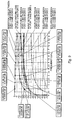
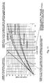
- FIGS. 7-11 The performance of the couplers of the present invention using the design methodology described above are set forth in FIGS. 7-11, wherein Figure 7 is a simulation results example for the basic directional coupler parameters over frequency optimized for wideband operation as shown in FIG. 1, wherein the impedance of all ports is 50 Ohms, Figure 8 is a simulation results example for the simplified directional coupler parameters over frequency optimized for wideband operation as shown in FIG. 2, wherein the impedance of all ports is 50 Ohms, Figure 9 is a simulation results example for the quad-band GSM directional coupler parameters over frequency optimized for GSM, DCS and PCS band operation as shown in FIG.
Landscapes
- Physics & Mathematics (AREA)
- General Physics & Mathematics (AREA)
- Amplifiers (AREA)
- Transmitters (AREA)
Abstract
Description
- The present invention relates to directional couplers used in RF applications.
- Directional couplers are used in many different RF applications such as power detection and control, test and measurement, mobile phones, and many others.
- Numerous types of couplers are known in the art. Micro-strip, strip-line, Lange-couplers and other directional couplers require a large size to obtain a reasonable coupling coefficient and low insertion loss over a wide frequency range. Consequently, these type of couplers increase total size and cost of, for example, mobile devices. L-C couplers used in current power detection applications (GSM, CDMA, WLAN, Bluetooth, etc.) are not "true" directional couplers and the coupling coefficient depends on a standing wave at the output (load VSWR dependent) resulting in incorrect power measurement and control. On-die implementation of micro-strip and other types of directional couplers is limited by high-frequency applications (microwave and millimeter-wave). The geometry of the coupler is directly proportional to the wavelength of the signal to be detected.
- What is desired, therefore, is a true directional coupler for RF applications that can be manufactured with a small geometry and at low cost.
- According to the present invention, a very small size "true" directional coupler has a coupling coefficient that is independent on load VSWR. The coupler uses coupled inductors with a compensation circuit including a resistor and a capacitor, or just a capacitor. The coupler can be made more than ten times smaller than the coupler area used in existing couplers. Wideband operation is suitable for many portable applications such as power detection and control for GSM, DCS-PCS, CDMA/WCDMA, Bluetooth, WLAN systems, and the like. The directional coupler of the present invention is easy and inexpensive to fabricate and can be manufactured using integrated circuits, printed circuit boards, low temperature co-fired ceramic implementations, or micro electro-mechanical systems ("MEMS"). A wide range of coupling coefficients can be realized by adjustment of the coupled inductance and the compensation circuit parameters. The coupler of the present invention has low insertion loss, and the coupling coefficient and insertion loss are tolerant to process and geometry variations. A small ballast resistor does not require large power dissipation over load VSWR variation. Optimal (minimum coupling between the load port and the coupling port) compensation capacitance is linearly dependent (positive slope) on the inductance coupling coefficient at a fixed inductance value and resistive loss. Optimal compensation capacitance is linearly dependent (negative slope) on inductance resistive loss at a fixed inductance value and coupling coefficient. Optimal compensation capacitance is linearly dependent (positive slope) on coupled inductance at fixed inductance resistive loss value and coupling coefficient.
- A first embodiment of the RF coupler according to the present invention includes an input port, a coupling port, a load port, a ballast resistor port, a compensation circuit coupled between the input port and the coupling port, and a coupled inductor having a first terminal coupled to the input port, a second terminal coupled to the coupling port, a third terminal coupled to the load port, and a fourth terminal coupled to the ballast resistor port.
- A second embodiment of the RF coupler according to the present invention includes a GSM input port, a power detector port, a DCS-PCS input port, a GSM output port, a ballast resistance port, a DCS-PCS output port, a first compensation circuit coupled between the GSM input port and the power detector port, a second compensation circuit coupled between the power detector port and the DCS-PCS input port, and a coupled inductor having a first terminal coupled to the GSM input port, a second terminal coupled to the power detector port, a third terminal coupled to the DCS-PCS input port, a fourth terminal coupled to the GSM output port, a fifth terminal coupled to the ballast resistance port, and a sixth terminal coupled to the DCS-PCS output port.
- A third embodiment of the RF coupler comprising includes an input port, a power detector port, an output port, a ballast resistor port, a compensation circuit coupled between the input port and the power detector port, a coupled inductor having a first terminal coupled to the input port, a second terminal coupled to the power detector port, a third terminal, and a fourth terminal coupled to the ballast resistor port, a shunt resistor coupled between the third terminal of the coupled inductor and ground, and a series resistor coupled between the third terminal of the coupled inductor and the output port.
- The aforementioned and other features and objects of the present invention and the manner of attaining them will become more apparent and the invention itself will be best understood by reference to the following description of a preferred embodiment taken in conjunction with the accompanying drawings, wherein:
- Figure 1 is schematic diagram of a true directional coupler circuit according to the present invention;
- Figure 2 is a schematic diagram of a simplified true directional coupler circuit according to the present invention;
- Figure 3 is a schematic diagram of a quad-band GSM directional coupler circuit according to the present invention;
- Figure 4 is a schematic diagram of a directional coupler circuit having an enhanced load VSWR tolerant capability according to the present invention;
- Figure 5 is a schematic diagram of a GSM power amplifier architecture with power control and enhanced load VSWR tolerance according to the present invention;
- Figure 6 is a schematic diagram of a quad-band GSM directional coupler circuit having an enhanced load VSWR tolerant capability according to the present invention;
- Figure 7 is a simulation results example for the basic directional coupler parameters over frequency optimized for wideband operation as shown in FIG. 1, wherein the impedance of all ports is 50 Ohms;
- Figure 8 is a simulation results example for the simplified directional coupler parameters over frequency optimized for wideband operation as shown in FIG. 2, wherein the impedance of all ports is 50 Ohms;
- Figure 9 is a simulation results example for the quad-band GSM directional coupler parameters over frequency optimized for GSM, DCS and PCS band operation as shown in FIG. 3, wherein the impedance of all ports is 50 Ohms;
- Figure 10 is a simulation results example for the GSM directional coupler with enhanced load VSWR tolerant capability parameters over frequency optimized for GSM, DCS and PCS band as shown in FIG. 4, wherein the impedance of all ports is 50 Ohms;
- Figure 11 is a simulation results example of coupler VSWR tolerance over load VSWR variation for the coupler of FIG. 4, wherein the impedance of
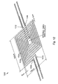
port 2 is varied; - Figure 12 is a layout diagram of an example of a single-layer coupled inductor according to the present invention;
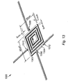
- Figure 13 is a layout diagram of an example of a dual-layer coupled inductor according to the present invention; and
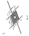
- Figure 14 is a layout diagram of an example of a triple-layer coupled inductor according to the present invention.
- Referring now to FIG. 1, an
RF coupler circuit 100 includes aninput port 102, acoupling port 106, aload port 104, aballast resistor port 108, acompensation circuit inductor 114 having a first terminal coupled to theinput port 102, a second terminal coupled to thecoupling port 106, a third terminal coupled to theload port 104, and a fourth terminal coupled to theballast resistor port 108. The coupledinductor 114 includes first andsecond inductors - In a typical example optimized for wideband (0.8-6 GHz) operation, the inductance of the first and
second inductors inductors coupler 100 includes aresistor 112 in series with acapacitor 110. The resistance ofresistor 112 is 21.4 ohms. The capacitance ofcapacitor 110 is 0.164 pF. - A simplified true
directional coupler 200 is shown in FIG. 2. Note that the compensation circuit includes onlycapacitor 110, whose value is 0.164 pF in a typical example. - A quad-band GSM directional coupler is shown in FIG. 3 including a
GSM input port 302, apower detector port 306, a DCS-PCS input port 310, aGSM output port 304, aballast resistance port 308, a DCS-PCS output port 312, afirst compensation circuit GSM input port 302 and thepower detector port 306, asecond compensation circuit power detector port 306 and the DCS-PCS input port 310, a coupledinductor 322 having a first terminal coupled to theGSM input port 302, a second terminal coupled to thepower detector port 306, a third terminal coupled to the DCS-PCS input port 310, a fourth terminal coupled to theGSM output port 304, a fifth terminal coupled to theballast resistance port 308, and a sixth terminal coupled to the DCS-PCS output port 312. The coupledinductor 322 includes first, second, andthird inductors - In a typical example optimized for GSM, DCS and PCS (0.8-1.9 Ghz) operation, the inductance of the first, second, and
third inductors coupler 300 includes aresistor 314 in series with acapacitor 316. The resistance ofresistor 314 is 21.5 ohms. The capacitance ofcapacitor 316 is 0.325 pF. The second compensation circuit forcoupler 300 includes aresistor 320 in series with acapacitor 318. The resistance ofresistor 320 is 21.5 ohms. The capacitance ofcapacitor 318 is 0.325 pF. If desired, the compensation circuits can include only a single capacitor. - Referring now to FIG. 4, an
RF coupler 400 having enhanced load VSWR tolerant capability includes aninput port 102; apower detector port 106, anoutput port 104, aballast resistor port 108, acompensation circuit 110 coupled between theinput port 102 and thepower detector port 106, a coupledinductor 114 having a first terminal coupled to theinput port 102, a second terminal coupled to thepower detector port 106, a third terminal, and a fourth terminal coupled to theballast resistor port 108, ashunt resistor 120 coupled between the third terminal of the coupledinductor 114 and ground, and a series resistor coupled between the third terminal of the coupledinductor 114 and theoutput port 104. The coupledinductor 114 includes first andsecond inductors - In a typical example optimized for GSM, DCS, and PCS (0.8-1.9 GHz) operation, the inductance of the first and
second inductors second inductors coupler 400 includes acapacitor 110 whose value is 0.33 pF. The value of the shunt resistor is 500 ohms, and the value of the series resistor is 3 ohms. - Referring now to FIG. 5, a GSM
power amplifier architecture 500 is shown using the directional RF coupler of the present invention.Power amplifier architecture 500 includes a main GSM power amplifier block 508 having an output coupled to anRF coupler 400 as is previously described.RF coupler 400 is also coupled to theRF output port 504. A power detector and control block 510 is coupled to thecontrol port 506, to the GSM power amplifier block 508, and to theRF coupler 400. Power detector and control block 510 includes anerror amplifier 512,parallel capacitor 514 andresistor 516,diode 518, and anattenuator 520. - Referring now to FIG. 6, a quad-band GSM directional coupler is shown as previously described with respect to FIG. 3. In addition to the previously described circuit components,
coupler 600 includes ashunt resistor 330 and aseries resistor 332 associated withGSM output port 312. If desired, these resistors can also be associated with DCS-PCS output port 304, or with both ports. - The following description refers to a detailed methodology for selecting the component values for the couplers of FIGS. 1-6 according to the present invention. Following a description of the methodology, the performance of the couplers of the present invention is set forth in FIGS. 7-11.
- After an appropriate technology is chosen, the design procedure uses high-frequency EM (electro-magnetic) and circuit simulation software - examples of which are AWR Microwave Office, Agilent ADS, and the like. As an initial matter the metal trace width and thickness of the coupled inductors should be chosen, which is dependent on RF power handling capability of the main signal path (input port to output port). This information can be found out in appropriate design rules of the particular technology chosen. As a rule, the wider and thicker the metal trace, the lower the insertion loss. The longer the metal trace is, the higher the insertion loss is. The inductor value is also dependent on proximity to other metal planes (such as ground) and other traces. All of these influences are fairly well developed by existing simulation software tools.
- Next, the inductance of the coupled inductors should be chosen. This inductance directly defines the final coupling coefficient between input port and coupled port of a coupler. As a rule of thumb, the higher the inductance value, the lower (in dB) the coupling coefficient. Coupling between the input port and the coupled port is also dependent on the coupling coefficient between coupled inductors. A higher coupling coefficient between the inductors results in a lower (in dB) coupling between input port and coupled port. The coupling coefficient between inductors is dependent on the distance between the two coils and as a rule the longer the distance, the lower the coupling. Particular implementation of a coupled inductors' technology defines coupling and can be found out by existing EM and circuit simulation software. For instance, simulating by EM software a particular coupled inductors' structure and then comparing with circuit simulation can give the correct value of coupling between the coils.
- Next, the compensation capacitor value should be chosen. The compensation capacitor value can be tuned in a circuit simulation until the minimum coupling between the output port and the coupled port is achieved (all ports should be loaded by 50 Ohms). Verify if the coupling coefficient between the input port and the coupled port has the desired value. If not, change the inductor value and repeat the simulation. When the desired coupling coefficient is achieved, add a compensation resistor in the circuit and tune this resistance value in the circuit simulator until the minimum coupling between the output port and the coupled port is achieved. The adding of the compensation resistor almost always does not change the coupling between the input port and the coupled port.
- The difference between the basic coupler with the compensation capacitor and the compensation resistor and the simplified coupler with just the compensation capacitor is in the minimum coupling value between the output port and the coupled port. The basic coupler has an advantage in this coupling (see appropriate simulation results below) although the simplified coupler has an advantage in implementation (compensation resistor is not necessary) and size.
- The placement and positioning of coupled inductors along with compensation capacitors and resistors is very flexible and it can be chosen as appropriate for a particular design. Referring to FIGS. 1-3, compensation circuits comprising a capacitor and resistor or just a capacitor can be inserted between the output port and the ballast resistor port instead of as shown in the originally proposed circuits. If desired, the compensation circuits can be inserted at the input and the output simultaneously. In both cases mentioned above a simulation should be done for best results in a particular implementation. Filtering components can be implemented at the input and output if desired as well as between the input and the output.
- Referring to FIG. 3, different compensation circuits can be connected to the GSM and the DCS-PCS ports. A simulation should be re-done if using different compensation circuits to assure the best performance for a particular implementation.
- Referring to FIGS. 1-3, the coupling port and ballast port resistors power handling capability can be facilitated so that the power dissipation therein is much less than in the main signal path between the input port and the output port. This results in a lower footprint comprising those components.
- Referring to FIG. 4, the compensation resistor along with capacitor can be added (as per the basic coupler structure). Series and shunt resistor values can be adjusted if required and they can be placed between input port and inductor as well. It is important to note that the insertion loss between the input port and the output port is higher when the series resistor is higher and the shunt resistor is lower. It should also be noted that the series resistor resistance adds to the series resistance of a coupled inductor, which should be taken into account during simulation. The coupled inductors' parameters can be adjusted, if required. An advantage of this circuit is that when the output port impedance is widely varied coupling between the input port and the coupling port remains essentially the same and at the same time the impedance variation at the input port is much less than at the output port. The power handling capability of the series resistor should be chosen for maximum RF power transfer between the input port and the output port when the output port is shorted to ground. The power handling capability of the shunt resistor should be chosen for maximum RF power transfer between the input port and the output port when the output port is open (disconnected).
- Referring to FIG. 5 the directional coupler block can have different component values from those described above, as is true as well for all of the couplers described herein as will be readily apparent to those skilled in the art. The power detector and control block can have a different architecture as per industry well known solutions.
- Referring to FIG. 6 all of the components and compensation circuitry can be adjusted as described above to suit the requirements of a particular implementation.
- The performance of the couplers of the present invention using the design methodology described above are set forth in FIGS. 7-11, wherein Figure 7 is a simulation results example for the basic directional coupler parameters over frequency optimized for wideband operation as shown in FIG. 1, wherein the impedance of all ports is 50 Ohms, Figure 8 is a simulation results example for the simplified directional coupler parameters over frequency optimized for wideband operation as shown in FIG. 2, wherein the impedance of all ports is 50 Ohms, Figure 9 is a simulation results example for the quad-band GSM directional coupler parameters over frequency optimized for GSM, DCS and PCS band operation as shown in FIG. 3, wherein the impedance of all ports is 50 Ohms, Figure 10 is a simulation results example for the GSM directional coupler with enhanced load VSWR tolerant capability parameters over frequency optimized for GSM, DCS and PCS band as shown in FIG. 4, wherein the impedance of all ports is 50 Ohms, and Figure 11 is a simulation results example of coupler VSWR tolerance over load VSWR variation for the coupler of FIG. 4, wherein the impedance of
port 2 is varied. - Referring generally to FIGS. 12-14, several examples of coupled inductors are shown that are appropriate for achieving the desirably small size for the couplers of the present invention. In general, the small size is possible because the values of the inductance of the coupled inductor, the compensation resistance, and the compensation capacitance are all correspondingly small. Suitable materials for the coupled inductors can include copper, gold, aluminum, and other conductors depending upon the fabrication technology chosen. As described above, the coupled inductors can be fabricated in an integrated circuit, on a printed circuit board, or in low temperature co-fired ceramic implementations, as well as MEMS.
- Referring now to FIG. 12 a single-layer coupled inductors layout example is shown as per the GSM coupler of FIG. 4. Coupled
inductor 1200 includes first andsecond inductors ports inductor - Referring now to FIG. 13 a dual-layer coupled inductor layout example is shown as per the wide-band coupler shown in FIGS. 1 and 2. Coupled
inductor 1300 includes first 1302 and second 1304 inductors having fourports inductor - Referring now to Fig. 14, where a triple-layer coupled inductors layout example is shown as per the quad-band GSM coupler shown in FIG. 3. Coupled
inductor 1400 includes first 1402, second 1404 and third 1406 inductors having sixports inductor -
- IC - Integrated Circuit.
- GSM - Global System for Mobile Communications.
- CDMA - Code Division Multiple Access.
- WCDMA - Wideband CDMA.
- WLAN - Wireless Local Area Networks.
- VSWR - Voltage Standing Wave Ratio.
- DCS - Digital Cellular System.
- PCS - Personal Communications Service.
- Bluetooth - Wireless personal area network standard.
- MEMS - Micro Electro-Mechanical System.
- Although the present invention has been described with reference to a preferred embodiment thereof, it will be understood that the invention is not limited to the details thereof. Various substitutions and modifications have been suggested in the foregoing description, and other will occur to those of ordinary skill in the art. Therefore, all such substitutions and modifications are intended to be embraced within the scope of the invention as defined in the appended claims.
Claims (16)
- An RF coupler comprising:an input port;a coupling port;a load port;a ballast resistor port;a compensation circuit coupled between the input port and the coupling port; anda coupled inductor having a first terminal coupled to the input port, a second terminal coupled to the coupling port, a third terminal coupled to the load port, and a fourth terminal coupled to the ballast resistor port.
- An RF coupler comprising:a GSM input port;a power detector port;a DCS-PCS input port;a GSM output port;a ballast resistance port;a DCS-PCS output port;a first compensation circuit coupled between the GSM input port and the power detector port;a second compensation circuit coupled between the power detector port and the DCS-PCS input port; anda coupled inductor having a first terminal coupled to the GSM input port, a second terminal coupled to the power detector port, a third terminal coupled to the DCS-PCS input port, a fourth terminal coupled to the GSM output port, a fifth terminal coupled to the ballast resistance port, and a sixth terminal coupled to the DCS-PCS output port.
- An RF coupler comprising:an input port;a power detector port;an output port;a ballast resistor port;a compensation circuit coupled between the input port and the power detector port;a coupled inductor having a first terminal coupled to the input port, a second terminal coupled to the power detector port, a third terminal, and a fourth terminal coupled to the ballast resistor port;a shunt resistor coupled between the third terminal of the coupled inductor and ground;a series resistor coupled between the third terminal of the coupled inductor and the output port.
- The RF coupler of any preceding claim wherein the coupled inductor comprises first and second inductors, and optionally a third inductor.
- The RF coupler of claim 4 wherein the coupled inductor comprises a single-layered coupled spiral of the first and second inductors.
- The RF coupler of claim 4 wherein the coupled inductor comprises a triple-layered coupled spiral of the first, second, and third inductors.
- The RF coupler of claim 4, 5 or 6 wherein the inductance of the inductors is 0.6 nH or 1.2 nH.
- The RF coupler of any preceding claim wherein the size of the coupled inductor is less than 0.1 mm x 0.2 mm.
- The RF coupler of any preceding claim wherein the or each compensation circuit comprises a resistor in series with a capacitor.
- The RF coupler of claim 9 wherein the resistance of the resistor is 21.4 or 21.5 ohms.
- The RF coupler of any preceding claim wherein the compensation circuit comprises a capacitor.
- The RF coupler of claim 9, 10 or 11 wherein the capacitance of the capacitor is 0.164 pF, 0.325 pF or 0.33 pF.
- The RF coupler of claim 2 or any claim appended thereto, further comprising a shunt and series resistor coupled to the GSM output port.
- The RF coupler of claim 2 or any claim appended thereto, further comprising a shunt and series resistor coupled to the DCS-PCS output port.
- The RF coupler of claim 3 or any claim appended thereto, or claim 13 or 14 wherein the resistance of the shunt resistor is 500 ohms.
- The RF coupler of claim 3 or any appended thereto, or claim 13 or 14 wherein the resistance of the series resistor is three ohms.
Applications Claiming Priority (1)
| Application Number | Priority Date | Filing Date | Title |
|---|---|---|---|
| US11/530,220 US7446626B2 (en) | 2006-09-08 | 2006-09-08 | Directional couplers for RF power detection |
Publications (3)
| Publication Number | Publication Date |
|---|---|
| EP1898224A2 true EP1898224A2 (en) | 2008-03-12 |
| EP1898224A3 EP1898224A3 (en) | 2012-01-11 |
| EP1898224B1 EP1898224B1 (en) | 2013-03-13 |
Family
ID=38962772
Family Applications (1)
| Application Number | Title | Priority Date | Filing Date |
|---|---|---|---|
| EP07253248A Active EP1898224B1 (en) | 2006-09-08 | 2007-08-17 | Directional couplers for RF power detection |
Country Status (3)
| Country | Link |
|---|---|
| US (2) | US7446626B2 (en) |
| EP (1) | EP1898224B1 (en) |
| CN (1) | CN101141137B (en) |
Cited By (1)
| Publication number | Priority date | Publication date | Assignee | Title |
|---|---|---|---|---|
| CN105826643A (en) * | 2016-04-26 | 2016-08-03 | 南京邮电大学 | Half-mode substrate integrated waveguide-based compact six-port circuit |
Families Citing this family (45)
| Publication number | Priority date | Publication date | Assignee | Title |
|---|---|---|---|---|
| US7612390B2 (en) * | 2004-02-05 | 2009-11-03 | Cree, Inc. | Heterojunction transistors including energy barriers |
| GB0800936D0 (en) | 2008-01-19 | 2008-02-27 | Fianium Ltd | A source of optical supercontinuum generation having a selectable pulse repetition frequency |
| US8442581B2 (en) * | 2009-06-05 | 2013-05-14 | Mediatek Inc. | System for the coexistence between a plurality of wireless communication modules |
| US9025583B2 (en) * | 2009-07-09 | 2015-05-05 | Mediatek Inc. | System for the coexistence between a plurality of wireless communication module sharing single antenna |
| US9504092B2 (en) | 2009-07-09 | 2016-11-22 | Mediatek Inc. | System for the coexistence between a plurality of wireless communications modules sharing single antenna |
| US8774722B2 (en) * | 2009-07-09 | 2014-07-08 | Mediatek Inc. | Systems and methods for reducing interference between a plurality of wireless communications modules |
| US9236896B2 (en) * | 2009-07-09 | 2016-01-12 | Mediatek Inc. | Systems and methods for coexistence of a plurality of wireless communications modules |
| CN102577104B (en) * | 2009-10-23 | 2015-01-14 | 日本碍子株式会社 | Synthesizer for Doherty Amplifier |
| KR101119910B1 (en) * | 2010-05-03 | 2012-02-29 | 한국과학기술원 | Mobile RFID Reader Transceiver System |
| CN101908881B (en) * | 2010-07-28 | 2012-11-07 | 锐迪科创微电子(北京)有限公司 | Directional coupler and radio-frequency power amplifier containing same |
| CN102243268B (en) * | 2010-07-29 | 2013-10-16 | 东南大学 | Micro-electro-mechanical directional coupling microwave power sensor and preparation method thereof |
| US8928428B2 (en) * | 2010-12-22 | 2015-01-06 | Rfaxis, Inc. | On-die radio frequency directional coupler |
| CN102208916B (en) * | 2011-03-15 | 2014-03-12 | 安徽白鹭电子科技有限公司 | Automatic compensation method for realizing power measurement based on capacitive reactance and inductive reactance of radio frequency circuit |
| US8699975B1 (en) | 2012-02-01 | 2014-04-15 | Triquint Semiconductor, Inc. | Directional coupler architecture for radio frequency power amplifier |
| US8606198B1 (en) | 2012-07-20 | 2013-12-10 | Triquint Semiconductor, Inc. | Directional coupler architecture for radio frequency power amplifier with complex load |
| US9356330B1 (en) | 2012-09-14 | 2016-05-31 | Anadigics, Inc. | Radio frequency (RF) couplers |
| CN106410358B (en) * | 2012-12-21 | 2019-08-23 | 上海联影医疗科技有限公司 | 3dB electric bridge power splitter |
| CN103066364B (en) * | 2012-12-28 | 2015-04-15 | 成都泰格微电子研究所有限责任公司 | Surface mounting microwave component feed point coupling circuit and standing wave and isolating control method thereof |
| CN103346373B (en) * | 2013-06-06 | 2016-05-25 | 中国科学院上海微系统与信息技术研究所 | Coupler is spent in a kind of broadband 180 of lumped parameter |
| US9535140B2 (en) | 2013-06-28 | 2017-01-03 | Infineon Technologies Ag | System and method for a transformer and a phase-shift network |
| CN103414002B (en) * | 2013-07-18 | 2015-09-16 | 南京邮电大学 | The interdigital coupling six-port network of a kind of co-planar waveguide |
| US8907702B1 (en) | 2013-08-26 | 2014-12-09 | Infineon Technologies Ag | System and method for a phase detector |
| US9319006B2 (en) | 2013-10-01 | 2016-04-19 | Infineon Technologies Ag | System and method for a radio frequency coupler |
| CN103529421B (en) * | 2013-10-29 | 2015-11-04 | 北京无线电计量测试研究所 | A kind of coupling mechanism calibration steps |
| JP2015115434A (en) * | 2013-12-11 | 2015-06-22 | 株式会社豊田中央研究所 | Magnetically coupled inductors and multiport converters |
| US9322858B2 (en) | 2014-02-04 | 2016-04-26 | Infineon Technologies Austria Ag | System and method for a phase detector |
| US10438735B2 (en) | 2014-07-22 | 2019-10-08 | Skyworks Solutions, Inc. | Ultra-high coupling factor monolithic transformers for integrated differential radio frequency amplifiers in system-on-chip devices |
| US9905902B2 (en) | 2014-07-24 | 2018-02-27 | Skyworks Solutions, Inc. | Zero insertion loss directional coupler for wireless transceivers with integrated power amplifiers |
| US9450639B2 (en) | 2014-07-28 | 2016-09-20 | Skyworks Solutions, Inc. | Complementary metal oxide semiconductor differential antenna transmit-receive switches with power combining circuitry for orthogonal frequency-division multiplexing systems |
| KR102579654B1 (en) * | 2015-01-09 | 2023-09-18 | 주식회사 제넥신 | Anemia treatment method using long-acting EPO preparations |
| CN107710503A (en) | 2015-04-28 | 2018-02-16 | 伯德技术集团股份有限公司 | Direct circuit directive overrurrent relay sensor with microstrip coupler |
| RU2601233C1 (en) * | 2015-08-04 | 2016-10-27 | Акционерное общество "Федеральный научно-производственный центр "Нижегородский научно-исследовательский институт радиотехники" | Method of designing microstrip directional couplers |
| RU2623666C1 (en) * | 2016-10-21 | 2017-06-28 | Федеральное государственное бюджетное учреждение науки Институт радиотехники и электроники им. В.А. Котельникова Российской академии наук | Three-channel directed coupler of microwave signal on magnetostatic waves |
| US10374280B2 (en) * | 2017-06-13 | 2019-08-06 | Raytheon Company | Quadrature coupler |
| US10587028B1 (en) | 2018-01-09 | 2020-03-10 | Berex Corporation | Radio frequency couplers with high directivity |
| WO2020129788A1 (en) * | 2018-12-17 | 2020-06-25 | 株式会社村田製作所 | Directional coupler and high frequency module |
| RU2717386C1 (en) * | 2019-05-27 | 2020-03-23 | Акционерное общество "Микроволновые системы" | Spiral ultra-wideband microstrip quadrature directional coupler |
| CN110600839B (en) * | 2019-09-18 | 2021-09-21 | 京东方科技集团股份有限公司 | Control substrate, liquid crystal phase shifter and manufacturing method of control substrate |
| US11674984B2 (en) | 2020-03-30 | 2023-06-13 | Keysight Technologies, Inc. | Directional power detector with low loss coupling network |
| CN111755792B (en) * | 2020-06-05 | 2022-03-04 | 唯捷创芯(天津)电子技术股份有限公司 | 3dB quadrature hybrid coupler, radio frequency front-end module and communication terminal |
| US11437992B2 (en) * | 2020-07-30 | 2022-09-06 | Mobix Labs, Inc. | Low-loss mm-wave CMOS resonant switch |
| DE112021006156T5 (en) * | 2020-11-24 | 2023-10-12 | KYOCERA AVX Components Corporation | Compact surface mount thin film coupler |
| CN112904079B (en) * | 2021-01-22 | 2024-04-16 | 新郦璞科技(上海)有限公司 | Bidirectional radio frequency power detector, working method and system |
| TW202243192A (en) * | 2021-03-08 | 2022-11-01 | 美商莫比克斯實驗公司 | Small-size millimeter wave on-chip 90-degree 3db couplers based on solenoid structures |
| CN114935686B (en) * | 2022-05-28 | 2024-06-18 | 上海柯渡医学科技股份有限公司 | Power detection tool and power detection method of magnetic resonance radio frequency system |
Citations (4)
| Publication number | Priority date | Publication date | Assignee | Title |
|---|---|---|---|---|
| US4216446A (en) | 1978-08-28 | 1980-08-05 | Motorola, Inc. | Quarter wave microstrip directional coupler having improved directivity |
| US4482873A (en) | 1982-09-16 | 1984-11-13 | Rockwell International Corporation | Printed hybrid quadrature 3 dB signal coupler apparatus |
| EP0641037A1 (en) | 1993-08-31 | 1995-03-01 | Hitachi Ferrite Ltd. | Strip line-type high-frequency element |
| US20030214365A1 (en) | 2002-05-20 | 2003-11-20 | Aharon Adar | High directivity multi-band coupled-line coupler for RF power amplifier |
Family Cites Families (14)
| Publication number | Priority date | Publication date | Assignee | Title |
|---|---|---|---|---|
| US4042887A (en) * | 1974-11-18 | 1977-08-16 | Q-Bit Corporation | Broad band amplifier |
| US6064872A (en) * | 1991-03-12 | 2000-05-16 | Watkins-Johnson Company | Totem pole mixer having grounded serially connected stacked FET pair |
| US5530922A (en) * | 1993-11-09 | 1996-06-25 | Motorola, Inc. | Power detector with matching impedance for radio frequency signal amplifiers |
| US6342681B1 (en) * | 1997-10-15 | 2002-01-29 | Avx Corporation | Surface mount coupler device |
| US6239668B1 (en) * | 1999-04-14 | 2001-05-29 | General Instrument Corporation | RF balun and transformer with shunt compensation transmission line |
| US6496708B1 (en) * | 1999-09-15 | 2002-12-17 | Motorola, Inc. | Radio frequency coupler apparatus suitable for use in a multi-band wireless communication device |
| US20030078037A1 (en) * | 2001-08-17 | 2003-04-24 | Auckland David T. | Methodology for portable wireless devices allowing autonomous roaming across multiple cellular air interface standards and frequencies |
| US7084832B2 (en) * | 2001-10-09 | 2006-08-01 | Plasma Control Systems, Llc | Plasma production device and method and RF driver circuit with adjustable duty cycle |
| US7405382B2 (en) * | 2002-04-08 | 2008-07-29 | Wayne Openlander | System for microwave enhanced chemistry |
| US6686812B2 (en) * | 2002-05-22 | 2004-02-03 | Honeywell International Inc. | Miniature directional coupler |
| US6825738B2 (en) * | 2002-12-18 | 2004-11-30 | Analog Devices, Inc. | Reduced size microwave directional coupler |
| DE10342611A1 (en) * | 2003-09-12 | 2005-04-14 | Hüttinger Elektronik Gmbh + Co. Kg | 90 ° hybrid for splitting or merging high-frequency power |
| US7245192B2 (en) * | 2003-12-08 | 2007-07-17 | Werlatone, Inc. | Coupler with edge and broadside coupled sections |
| US6972639B2 (en) * | 2003-12-08 | 2005-12-06 | Werlatone, Inc. | Bi-level coupler |
-
2006
- 2006-09-08 US US11/530,220 patent/US7446626B2/en active Active
-
2007
- 2007-08-17 EP EP07253248A patent/EP1898224B1/en active Active
- 2007-09-07 CN CN2007101544563A patent/CN101141137B/en active Active
-
2008
- 2008-09-11 US US12/208,960 patent/US7576626B2/en active Active
Patent Citations (4)
| Publication number | Priority date | Publication date | Assignee | Title |
|---|---|---|---|---|
| US4216446A (en) | 1978-08-28 | 1980-08-05 | Motorola, Inc. | Quarter wave microstrip directional coupler having improved directivity |
| US4482873A (en) | 1982-09-16 | 1984-11-13 | Rockwell International Corporation | Printed hybrid quadrature 3 dB signal coupler apparatus |
| EP0641037A1 (en) | 1993-08-31 | 1995-03-01 | Hitachi Ferrite Ltd. | Strip line-type high-frequency element |
| US20030214365A1 (en) | 2002-05-20 | 2003-11-20 | Aharon Adar | High directivity multi-band coupled-line coupler for RF power amplifier |
Cited By (2)
| Publication number | Priority date | Publication date | Assignee | Title |
|---|---|---|---|---|
| CN105826643A (en) * | 2016-04-26 | 2016-08-03 | 南京邮电大学 | Half-mode substrate integrated waveguide-based compact six-port circuit |
| CN105826643B (en) * | 2016-04-26 | 2018-05-18 | 南京邮电大学 | Compact six-port circuit based on half module substrate integrated wave guide |
Also Published As
| Publication number | Publication date |
|---|---|
| CN101141137A (en) | 2008-03-12 |
| US20080061903A1 (en) | 2008-03-13 |
| EP1898224B1 (en) | 2013-03-13 |
| US20090009260A1 (en) | 2009-01-08 |
| US7576626B2 (en) | 2009-08-18 |
| CN101141137B (en) | 2012-08-15 |
| US7446626B2 (en) | 2008-11-04 |
| EP1898224A3 (en) | 2012-01-11 |
Similar Documents
| Publication | Publication Date | Title |
|---|---|---|
| EP1898224B1 (en) | Directional couplers for RF power detection | |
| US8314663B2 (en) | Directional coupler | |
| US8928428B2 (en) | On-die radio frequency directional coupler | |
| JP6280985B2 (en) | Compact wireless directional coupler for cellular applications | |
| US20100194489A1 (en) | Directional coupler including impedance matching and impedance transforming attenuator | |
| US8330551B2 (en) | Dual band high frequency amplifier using composite right/left handed transmission line | |
| US9281797B2 (en) | High-frequency device and directional coupler | |
| WO2004062026A1 (en) | Reduced size microwave directional coupler | |
| US10714806B2 (en) | Bi-directional coupler | |
| Liu et al. | A novel patterned ground structure with shunt and series lumped elements for synthesizing absorption common-mode filters | |
| US7821352B1 (en) | Ultra-wideband, directional coupler and method of implementation | |
| US10438732B2 (en) | Monolithic wideband trifilar transformer | |
| US10587028B1 (en) | Radio frequency couplers with high directivity | |
| US7746193B2 (en) | Miniature 180 degree hybrid coupler | |
| Liang et al. | Design and modeling of compact on-chip transformer/balun using multi-level metal windings for RF integrated circuits | |
| Hausman | Microwave power amplifier design with MMIC modules | |
| Liu et al. | Small form-factor integrated balun with complex impedance matching | |
| Kapur et al. | Synthesis of optimal on-chip baluns | |
| Heuermann | Passive RF Components Made from Concentrated Components | |
| CN114188687B (en) | Power divider, power divider chip and electronic equipment | |
| US20250062737A1 (en) | Systems and methods for frequency equalization and temperature compensation in radio frequency devices | |
| Shibata et al. | Characterization of Multi-Layer Ceramic Chip Capacitors up to mm-Wave Frequencies for High-Speed Digital Signal Coupling | |
| Campbell et al. | Monolithic GaAs passive low pass 3 dB in-phase splitter/combiner | |
| CN118523742A (en) | Coupling device based on RLC network | |
| Chi-kit | Design Study of Multilayer Lumped Element Balanced LNA Using LTCC Technology |
Legal Events
| Date | Code | Title | Description |
|---|---|---|---|
| PUAI | Public reference made under article 153(3) epc to a published international application that has entered the european phase |
Free format text: ORIGINAL CODE: 0009012 |
|
| AK | Designated contracting states |
Kind code of ref document: A2 Designated state(s): AT BE BG CH CY CZ DE DK EE ES FI FR GB GR HU IE IS IT LI LT LU LV MC MT NL PL PT RO SE SI SK TR |
|
| AX | Request for extension of the european patent |
Extension state: AL BA HR MK YU |
|
| PUAL | Search report despatched |
Free format text: ORIGINAL CODE: 0009013 |
|
| AK | Designated contracting states |
Kind code of ref document: A3 Designated state(s): AT BE BG CH CY CZ DE DK EE ES FI FR GB GR HU IE IS IT LI LT LU LV MC MT NL PL PT RO SE SI SK TR |
|
| AX | Request for extension of the european patent |
Extension state: AL BA HR MK RS |
|
| RIC1 | Information provided on ipc code assigned before grant |
Ipc: H01P 5/18 20060101AFI20111205BHEP Ipc: H03H 7/48 20060101ALI20111205BHEP Ipc: G01R 27/06 20060101ALI20111205BHEP |
|
| 17P | Request for examination filed |
Effective date: 20120711 |
|
| REG | Reference to a national code |
Ref country code: DE Ref legal event code: R079 Ref document number: 602007029014 Country of ref document: DE Free format text: PREVIOUS MAIN CLASS: G01R0027060000 Ipc: H01P0005180000 |
|
| AKX | Designation fees paid |
Designated state(s): DE FR GB IT |
|
| GRAP | Despatch of communication of intention to grant a patent |
Free format text: ORIGINAL CODE: EPIDOSNIGR1 |
|
| RIC1 | Information provided on ipc code assigned before grant |
Ipc: H01P 5/18 20060101AFI20120907BHEP Ipc: G01R 27/06 20060101ALI20120907BHEP Ipc: H03H 7/48 20060101ALI20120907BHEP |
|
| GRAS | Grant fee paid |
Free format text: ORIGINAL CODE: EPIDOSNIGR3 |
|
| GRAA | (expected) grant |
Free format text: ORIGINAL CODE: 0009210 |
|
| AK | Designated contracting states |
Kind code of ref document: B1 Designated state(s): DE FR GB IT |
|
| REG | Reference to a national code |
Ref country code: GB Ref legal event code: FG4D |
|
| REG | Reference to a national code |
Ref country code: DE Ref legal event code: R096 Ref document number: 602007029014 Country of ref document: DE Effective date: 20130502 |
|
| PLBE | No opposition filed within time limit |
Free format text: ORIGINAL CODE: 0009261 |
|
| STAA | Information on the status of an ep patent application or granted ep patent |
Free format text: STATUS: NO OPPOSITION FILED WITHIN TIME LIMIT |
|
| 26N | No opposition filed |
Effective date: 20131216 |
|
| PG25 | Lapsed in a contracting state [announced via postgrant information from national office to epo] |
Ref country code: IT Free format text: LAPSE BECAUSE OF FAILURE TO SUBMIT A TRANSLATION OF THE DESCRIPTION OR TO PAY THE FEE WITHIN THE PRESCRIBED TIME-LIMIT Effective date: 20130313 |
|
| REG | Reference to a national code |
Ref country code: DE Ref legal event code: R097 Ref document number: 602007029014 Country of ref document: DE Effective date: 20131216 |
|
| GBPC | Gb: european patent ceased through non-payment of renewal fee |
Effective date: 20130817 |
|
| PG25 | Lapsed in a contracting state [announced via postgrant information from national office to epo] |
Ref country code: GB Free format text: LAPSE BECAUSE OF NON-PAYMENT OF DUE FEES Effective date: 20130817 |
|
| REG | Reference to a national code |
Ref country code: FR Ref legal event code: PLFP Year of fee payment: 10 |
|
| REG | Reference to a national code |
Ref country code: FR Ref legal event code: PLFP Year of fee payment: 11 |
|
| REG | Reference to a national code |
Ref country code: FR Ref legal event code: PLFP Year of fee payment: 12 |
|
| REG | Reference to a national code |
Ref country code: DE Ref legal event code: R082 Ref document number: 602007029014 Country of ref document: DE Representative=s name: PAGE, WHITE & FARRER GERMANY LLP, DE |
|
| PGFP | Annual fee paid to national office [announced via postgrant information from national office to epo] |
Ref country code: FR Payment date: 20200721 Year of fee payment: 14 |
|
| PG25 | Lapsed in a contracting state [announced via postgrant information from national office to epo] |
Ref country code: FR Free format text: LAPSE BECAUSE OF NON-PAYMENT OF DUE FEES Effective date: 20210831 |
|
| REG | Reference to a national code |
Ref country code: DE Ref legal event code: R081 Ref document number: 602007029014 Country of ref document: DE Owner name: STMICROELECTRONICS INTERNATIONAL N.V., CH Free format text: FORMER OWNER: STMICROELECTRONICS LTD. (HONG KONG), HONG KONG, HK |
|
| PGFP | Annual fee paid to national office [announced via postgrant information from national office to epo] |
Ref country code: DE Payment date: 20250724 Year of fee payment: 19 |
|
| REG | Reference to a national code |
Ref country code: DE Ref legal event code: R082 Ref document number: 602007029014 Country of ref document: DE Representative=s name: WESTPHAL, MUSSGNUG & PARTNER PATENTANWAELTE MI, DE |