EP1898196A2 - Method for fabricating capacitive pressure sensor and capacitive pressure sensor fabricated thereby - Google Patents
Method for fabricating capacitive pressure sensor and capacitive pressure sensor fabricated thereby Download PDFInfo
- Publication number
- EP1898196A2 EP1898196A2 EP07002840A EP07002840A EP1898196A2 EP 1898196 A2 EP1898196 A2 EP 1898196A2 EP 07002840 A EP07002840 A EP 07002840A EP 07002840 A EP07002840 A EP 07002840A EP 1898196 A2 EP1898196 A2 EP 1898196A2
- Authority
- EP
- European Patent Office
- Prior art keywords
- etching
- capacitor
- silicon substrate
- pressure sensor
- depositing
- Prior art date
- Legal status (The legal status is an assumption and is not a legal conclusion. Google has not performed a legal analysis and makes no representation as to the accuracy of the status listed.)
- Withdrawn
Links
Images


Classifications
-
- G—PHYSICS
- G01—MEASURING; TESTING
- G01L—MEASURING FORCE, STRESS, TORQUE, WORK, MECHANICAL POWER, MECHANICAL EFFICIENCY, OR FLUID PRESSURE
- G01L9/00—Measuring steady of quasi-steady pressure of fluid or fluent solid material by electric or magnetic pressure-sensitive elements; Transmitting or indicating the displacement of mechanical pressure-sensitive elements, used to measure the steady or quasi-steady pressure of a fluid or fluent solid material, by electric or magnetic means
- G01L9/0041—Transmitting or indicating the displacement of flexible diaphragms
- G01L9/0072—Transmitting or indicating the displacement of flexible diaphragms using variations in capacitance
- G01L9/0073—Transmitting or indicating the displacement of flexible diaphragms using variations in capacitance using a semiconductive diaphragm
-
- G—PHYSICS
- G01—MEASURING; TESTING
- G01L—MEASURING FORCE, STRESS, TORQUE, WORK, MECHANICAL POWER, MECHANICAL EFFICIENCY, OR FLUID PRESSURE
- G01L1/00—Measuring force or stress, in general
- G01L1/14—Measuring force or stress, in general by measuring variations in capacitance or inductance of electrical elements, e.g. by measuring variations of frequency of electrical oscillators
-
- Y—GENERAL TAGGING OF NEW TECHNOLOGICAL DEVELOPMENTS; GENERAL TAGGING OF CROSS-SECTIONAL TECHNOLOGIES SPANNING OVER SEVERAL SECTIONS OF THE IPC; TECHNICAL SUBJECTS COVERED BY FORMER USPC CROSS-REFERENCE ART COLLECTIONS [XRACs] AND DIGESTS
- Y10—TECHNICAL SUBJECTS COVERED BY FORMER USPC
- Y10T—TECHNICAL SUBJECTS COVERED BY FORMER US CLASSIFICATION
- Y10T29/00—Metal working
- Y10T29/43—Electric condenser making
Definitions
- the present invention relates to a capacitive pressure sensor, and more particularly to a method for fabricating a capacitive pressure sensor, which has an area changed according to a variation of external pressure so that output is linearly changed according to input, and uses hafnium oxide having excellent insulating properties and a high dielectric constant as an insulating material of a capacitor so as to have high sensitivity, and a capacitive pressure sensor fabricated thereby.
- Pressure sensors are elements for measuring an absolute pressure or a relative pressure, and are divided into strain gauge-type metal pressure sensors, piezoresistive pressure sensors, piezoelectric pressure sensors, MOSFET pressure sensors, piezojunction pressure sensors, optical fiber pressures sensors, and capacitive pressure sensors, according to sensing principles.
- the above pressure sensors, except for the metal pressure sensors using metal, are fabricated by the micromachining technique using a semiconductor substance, i.e., silicon.
- Capacitive pressure sensors use a principle in which the capacitance of a parallel plate capacitor between a silicon thin film diaphragm (membrane) and a support is changed according to a variation of an interval between two electrodes due to the deflection of the silicon thin film diaphragm (i.e., the deformation of the membrane) according to a variation of pressure supplied from the outside.
- An absolute pressure sensor is a capacitive pressure sensor, which is fabricated under the condition that a diaphragm is closed, and thus senses an external pressure on the basis of a designated pressure in a reference pressure chamber.
- the absolute pressure sensor is completely isolated from the outside, thus being not influenced by surrounding substances.
- air in the reference pressure chamber is compressed to generate nonlinearity, and is expanded according to an increase in temperature to generate offset and temperature drift.
- a relative pressure sensor is a capacitive pressure sensor, which has a reference pressure chamber opened by perforating a glass portion, and thus senses relative pressures of two portions, i.e., a difference of pressures between upper and lower portions of a diaphragm.
- the relative pressure sensor is opened to the outside, thus being easily influenced by surrounding substances.
- the reference pressure chamber is not closed, the relative pressure sensor is not influenced by the compression or expansion of the air in the reference pressure chamber.
- the capacitive pressure sensors which detect a capacitance between two electrodes using the deflection of a diaphragm (the deformation of a membrane), has a value of sensitivity several hundred times as high as piezoresistive pressure sensors (higher sensitivity), and has higher stability (lower temperature coefficient and stronger structure) and smaller power consumption (lower power consumption rate) than piezoresistive pressure sensors.
- FIGS. 1A to 1F illustrate a process for fabricating a conventional capacitive pressure sensor. Since a variation in capacitance according to a variation in pressure is in the range of picofarad, in order to remove a parasitic capacitance between two electrodes, a lower electrode 14 is formed on a glass substrate 13, an upper electrode 12 is formed on a silicon substrate 11, and the two substrates 13 and 11 are hybrid-bonded using an electric (anodic) bonding method.
- FIG. 1A illustrates the silicon substrate 11 used as an upper substrate.
- the front surface of the silicon substrate 11 is etched to a designated depth by dry etching, and the upper electrode 12 of a capacitor, which is made of a metal, is formed on the etched region.
- FIG. 1C illustrates the glass substrate 13 used as a lower substrate. As shown in FIG. 3D, the lower electrode 14 is formed on the glass substrate 13.
- the two electrodes 11 and 13 provided with the upper and lower electrodes 12 and 14 are hybrid-bonded using the electric (anodic) bonding method.
- the rear surface of the silicon substrate 11 is etched by anisotropic chemical etching, thus forming a membrane. Thereby, the fabrication of a capacitive pressure sensor is completed.
- the above capacitive pressure sensor electrically reads change of a distance between two electrodes of the capacitor through the movement of the membrane according to a variation of pressure.
- the above conventional capacitive pressure sensor has excellent sensitivity and temperature characteristics (i.e., has higher sensitivity and is less sensitive to a variation of temperature), compared to a piezoresistive pressure sensor, thus being applied to many fields.
- the capacitance is in inverse proportion to the distance between two electrodes, and the membrane does not downwardly move horizontally but is bent when external pressure is applied thereto, a variation of capacitance according to a variation of pressure cannot exhibit linearity. That is, the linearity of output according to input is poor, and thus, it is difficult to achieve sensor compensation.
- the usable pressure range is narrow, the substantial use of the conventional capacitive pressure sensor is restricted.
- Korean Patent Publication No. 96-006113 discloses a semiconductor capacitive pressure sensor, in which a capacitor electrode of a silicon diaphragm is deformed into a cross shape to improve nonlinear response characteristics.
- Korean Patent Registration No. 10-0404904 discloses a differential capacitive pressure sensor and a method for fabricating the same, in which two sensing capacitors are disposed at both sides and a single-layered sacrificial layer is used to improve nonlinear characteristics of the pressure sensor and the intervals between upper and lower electrodes of the two sensing capacitors become equal using the single-layered sacrificial layer to simplify a fabricating process, and variations of capacitance of the sensing capacitors due to displacement become equal to increase the linearity of the pressure sensor.
- Satoshi Yamamoto et al. disclose a capacitive pressure sensor having high linearity, in which a distance between two electrodes of a capacitor is changed according to a variation of pressure.
- Such a capacitive pressure sensor has a principle in that when pressure with a designated value or more is applied to the capacitive pressure sensor, the capacitive pressure sensor is operated under the condition that the upper electrode, i.e. the membrane, contacts an insulating material deposited on the lower electrode.
- the present invention has been made in view of the above problems, and it is an object of the present invention to provide a method for fabricating a capacitive pressure sensor, in which a distance between two electrodes of a capacitor is not changed but an area of the pressure sensor is changed, according to a variation of pressure so that output is linearly changed according to input, and hafnium oxide having excellent insulating properties and a high dielectric constant is used as an insulating material of the capacitor to increase the capacitance and thus to increase the sensitivity, and a capacitive pressure sensor fabricated thereby.
- a method for fabricating a capacitive pressure sensor comprising etching the front surface of a silicon substrate to a designated depth; depositing an etching stopper, for stopping etching of the rear surface of the silicon substrate, on the surface of the silicon substrate; depositing an upper electrode of a capacitor on the surface of the etching stopper; depositing an insulating surface of the capacitor on the surface of the upper electrode; depositing a lower electrode of the capacitor on the surface of the insulating surface to form the capacitor; forming a metal pad electrode on the front surface of a glass substrate; hybrid-bonding the lower electrode of the capacitor of the silicon substrate and the metal pad electrode of the glass substrate using an electric (anodic) bonding method; etching the rear surface of the silicon substrate bonded to the glass substrate to selectively expose the etching stopper and thus to form a membrane; and removing the exposed region of the etching stopper by wet etching.
- anisotropic chemical etching using potassium hydroxide (KOH) or ethylene diamine pyrocatechol (EDP) may be performed and silicon nitride (Si x N y ), silicon dioxide (SiO 2 ) or a metal, selected from the group consisting of gold (Au) and chrome (Cr), may be used as a mask material.
- dry etching may be performed and photoresist or a metal, selected from the group consisting of gold (Au), chrome (Cr) and aluminum (A1), may be used as a mask material.
- the etching stopper for stopping the etching of the rear surface of the silicon substrate by anisotropic chemical etching using potassium hydroxide (KOH) or ethylene diamine pyrocatechol (EDP), may be made of silicon dioxide (SiO 2 ), in the depositing of the etching stopper.
- KOH potassium hydroxide
- EDP ethylene diamine pyrocatechol
- the upper electrode may be made of doped polysilicon, in the depositing of the upper electrode of the capacitor.
- the insulating layer may be made of hafnium oxide, in the depositing of the insulating layer of the capacitor.
- the lower electrode may be made of doped polysilicon, in the depositing of the lower electrode.
- the rear surface of the silicon substrate may be etched by anisotropic chemical etching, in the etching of the rear surface of the silicon substrate, and thus the capacitor may be formed in the shape of the membrane having a three-layer structure moving according to a variation of pressure, in the removing of the exposed region of the etching stopper.
- the above capacitive pressure sensor of the present invention is characterized in that the capacitor is formed in the shape of the membrane having a three-layer structure, the area of the capacitor is changed according to a variation of external pressure, and hafnium oxide having excellent insulating properties and a high dielectric constant is used as the insulating layer.
- FIGS. 2A to 2K a method for fabricating a capacitive pressure sensor having high linearity in accordance with the present invention will be described with reference to FIGS. 2A to 2K.
- a silicon substrate 20 is used to form a membrane 30, and a glass substrate 25 is used to form a bonding metal pad electrode 26.
- the silicon substrate 20 is prepared.
- the front surface of the silicon substrate 20 is etched to a designated depth in a first step (S1).
- Si x N y silicon nitride
- SiO 2 silicon dioxide
- metal such as gold (Au) or chrome (Cr)
- photoresist, or metal such as gold (Au), chrome (Cr), or aluminum (A1), is used as a mask material.
- silicon dioxide SiO 2
- SiO 2 silicon dioxide
- etching stopper 21 for stopping anisotropic chemical etching using potassium hydroxide (KOH) or ethylene diamine pyrocatechol (EDP), which will be later described in an eighth step (S8), in a second step (2).
- doped polysilicon is deposited on the surface of the etching stopper 21, thus forming an upper electrode 22 of a capacitor, in a third step (S3).
- hafnium oxide having excellent insulating properties and a high dielectric constant is deposited on the surface of the upper electrode 22, thus forming an insulating layer 23, in a fourth step (S4). Since the hafnium oxide has excellent insulating properties, the use of the insulating layer 23 with a small thickness increases the capacitance of the capacitor 29.
- doped polysilicon is deposited on the insulating layer 23, thus forming a lower electrode 24 of the capacitor 29, in a fifth step (S5). Thereby, the formation of the capacitor 29 is completed.
- a metal pad electrode 26 is formed on the front surface of the glass substrate 25 in a sixth step (S6). Thereafter, as shown in FIG. 2H, the lower electrode 24 of the capacitor 29 of the silicon substrate 20 and the metal pad electrode 26 of the glass substrate 25 are hybrid-bonded using an electric (anodic) bonding method in a seventh step (S7).
- the rear surface of the silicon substrate 20 is etched by anisotropic chemical etching using potassium hydroxide (KOH) or ethylene diamine pyrocatechol (EDP), thus selectively exposing the etching stopper 21, in the eighth step (S8).
- KOH potassium hydroxide
- EDP ethylene diamine pyrocatechol
- Si x N y silicon dioxide
- SiO 2 silicon dioxide
- metal such as gold (Au) or chrome (Cr)
- silicon dioxide (SiO 2 ) is used as the etching stopper 21.
- the membrane 30 having the above three-layer structure includes the upper electrode 22, the insulating layer 23, and the lower electrode 24.
- FIGS. 3A and 3B are schematic sectional views illustrating the operation of the capacitive pressure sensor of the present invention, which is fabricated by the above method.
- the membrane 30 When external pressure is not applied to the membrane 30, the membrane 30 maintains its level state, as shown in FIG. 3A, and when external pressure is applied to the membrane 30, the membrane 30 is concavely bent into an arched state and thus has an increased area, as shown in FIG. 3B. Since the area of the membrane 30 means the area of the capacitor, the capacitance of the capacitor is changed.
- the capacitance is in proportion to the area of the membrane 30, and when external pressure is applied to the membrane 30, the membrane 30 is concavely bent from the level state into the arched state. Accordingly, a variation of capacitance according to a variation of pressure exhibits linearity.
- the present invention provides a method for fabricating a capacitive pressure sensor, which has an area changed according to a variation of external pressure so that output is linearly changed according to input, and uses hafnium oxide having a high dielectric constant as an insulating material to increase the capacitance and thus to increase the sensitivity, and a capacitive pressure sensor fabricated thereby, thus allowing the capacitive pressure sensor to have high linearity and sensitivity.
Landscapes
- Physics & Mathematics (AREA)
- General Physics & Mathematics (AREA)
- Measuring Fluid Pressure (AREA)
- Pressure Sensors (AREA)
Abstract
Disclosed is a method for fabricating a capacitive pressure sensor and a capacitive pressure sensor fabricated thereby. The method includes etching the front surface of a silicon substrate to a designated depth; depositing an etching stopper, for stopping etching of the rear surface of the silicon substrate, on the surface of the silicon substrate; depositing an upper electrode of a capacitor on the surface of the etching stopper; depositing an insulating surface of the capacitor on the surface of the upper electrode; depositing a lower electrode of the capacitor on the surface of the insulating surface to form the capacitor; forming a metal pad electrode on the front surface of a glass substrate; hybrid-bonding the lower electrode of the capacitor of the silicon substrate and the metal pad electrode of the glass substrate using an electric (anodic) bonding method; etching the rear surface of the silicon substrate bonded to the glass substrate to selectively expose the etching stopper and thus to form a membrane; and removing the exposed region of the etching stopper by wet etching. The capacitive pressure sensor has an area changed according to a variation of external pressure so that output is linearly changed according to input, and uses hafnium oxide having a high dielectric constant as an insulating material to have high capacitance, thus being improved in sensitivity.





Description
- The present invention relates to a capacitive pressure sensor, and more particularly to a method for fabricating a capacitive pressure sensor, which has an area changed according to a variation of external pressure so that output is linearly changed according to input, and uses hafnium oxide having excellent insulating properties and a high dielectric constant as an insulating material of a capacitor so as to have high sensitivity, and a capacitive pressure sensor fabricated thereby.
- Researches in semiconductor pressure sensors using a micromachining technique employing a semiconductor fabricating process have been going on now. Semiconductor pressure sensors obtained by the micromachining technique are widely applied to vehicle system, industrial control, environmental monitoring, and bio-medical diagnosis fields.
- Pressure sensors are elements for measuring an absolute pressure or a relative pressure, and are divided into strain gauge-type metal pressure sensors, piezoresistive pressure sensors, piezoelectric pressure sensors, MOSFET pressure sensors, piezojunction pressure sensors, optical fiber pressures sensors, and capacitive pressure sensors, according to sensing principles. The above pressure sensors, except for the metal pressure sensors using metal, are fabricated by the micromachining technique using a semiconductor substance, i.e., silicon.
- Capacitive pressure sensors use a principle in which the capacitance of a parallel plate capacitor between a silicon thin film diaphragm (membrane) and a support is changed according to a variation of an interval between two electrodes due to the deflection of the silicon thin film diaphragm (i.e., the deformation of the membrane) according to a variation of pressure supplied from the outside.
- The above capacitive pressure sensors are classified into absolute pressure sensors and relative pressure sensors. An absolute pressure sensor is a capacitive pressure sensor, which is fabricated under the condition that a diaphragm is closed, and thus senses an external pressure on the basis of a designated pressure in a reference pressure chamber. The absolute pressure sensor is completely isolated from the outside, thus being not influenced by surrounding substances. However, air in the reference pressure chamber is compressed to generate nonlinearity, and is expanded according to an increase in temperature to generate offset and temperature drift. A relative pressure sensor is a capacitive pressure sensor, which has a reference pressure chamber opened by perforating a glass portion, and thus senses relative pressures of two portions, i.e., a difference of pressures between upper and lower portions of a diaphragm. The relative pressure sensor is opened to the outside, thus being easily influenced by surrounding substances. However, since the reference pressure chamber is not closed, the relative pressure sensor is not influenced by the compression or expansion of the air in the reference pressure chamber.
- The capacitive pressure sensors, which detect a capacitance between two electrodes using the deflection of a diaphragm (the deformation of a membrane), has a value of sensitivity several hundred times as high as piezoresistive pressure sensors (higher sensitivity), and has higher stability (lower temperature coefficient and stronger structure) and smaller power consumption (lower power consumption rate) than piezoresistive pressure sensors.
- FIGS. 1A to 1F illustrate a process for fabricating a conventional capacitive pressure sensor. Since a variation in capacitance according to a variation in pressure is in the range of picofarad, in order to remove a parasitic capacitance between two electrodes, a
lower electrode 14 is formed on aglass substrate 13, anupper electrode 12 is formed on asilicon substrate 11, and the twosubstrates - First, FIG. 1A illustrates the
silicon substrate 11 used as an upper substrate. As shown in FIG. 1B, the front surface of thesilicon substrate 11 is etched to a designated depth by dry etching, and theupper electrode 12 of a capacitor, which is made of a metal, is formed on the etched region. - FIG. 1C illustrates the
glass substrate 13 used as a lower substrate. As shown in FIG. 3D, thelower electrode 14 is formed on theglass substrate 13. - As shown in FIG. 1E, the two
electrodes lower electrodes - Finally, as shown in FIG. 1F, the rear surface of the
silicon substrate 11 is etched by anisotropic chemical etching, thus forming a membrane. Thereby, the fabrication of a capacitive pressure sensor is completed. - The above capacitive pressure sensor electrically reads change of a distance between two electrodes of the capacitor through the movement of the membrane according to a variation of pressure.
- The above conventional capacitive pressure sensor has excellent sensitivity and temperature characteristics (i.e., has higher sensitivity and is less sensitive to a variation of temperature), compared to a piezoresistive pressure sensor, thus being applied to many fields. However, since the capacitance is in inverse proportion to the distance between two electrodes, and the membrane does not downwardly move horizontally but is bent when external pressure is applied thereto, a variation of capacitance according to a variation of pressure cannot exhibit linearity. That is, the linearity of output according to input is poor, and thus, it is difficult to achieve sensor compensation. Thereby, since the usable pressure range is narrow, the substantial use of the conventional capacitive pressure sensor is restricted.
- Accordingly, in order to improve the nonlinearity of the capacitive pressure sensor, various researches in the structural deformation of the capacitive pressure sensor have been carried out.
- Various attempts for deforming the structure of the capacitive pressure sensor are taken, as follows.
-
Korean Patent Publication No. 96-006113 - See Aziz Ettouhami et al. (2004). A novel capacitive pressure sensor structure with high sensitivity and quasi-linear response. Morocco. Comptes rendus. Mecanique. pp. 141-162.
- In a general capacitive pressure sensor, when a membrane has a small thickness in order to increase the sensitivity of the capacitive pressure sensor, the linearity of the capacitive pressure sensor is deteriorated. However, Aziz Ettouhami et al. solve the above nonlinearity problem using a series capacitor, thus improving the sensitivity and the linearity of a capacitive pressure sensor.
- Further, see Satoshi Yamamoto et al. (2003). Touch mode capacitive pressure sensor for passive tire monitoring system. Japan. IEEJ transactions on sensors and micromachines. pp. 9-15.
- Satoshi Yamamoto et al. disclose a capacitive pressure sensor having high linearity, in which a distance between two electrodes of a capacitor is changed according to a variation of pressure. Such a capacitive pressure sensor has a principle in that when pressure with a designated value or more is applied to the capacitive pressure sensor, the capacitive pressure sensor is operated under the condition that the upper electrode, i.e. the membrane, contacts an insulating material deposited on the lower electrode.
- Therefore, the present invention has been made in view of the above problems, and it is an object of the present invention to provide a method for fabricating a capacitive pressure sensor, in which a distance between two electrodes of a capacitor is not changed but an area of the pressure sensor is changed, according to a variation of pressure so that output is linearly changed according to input, and hafnium oxide having excellent insulating properties and a high dielectric constant is used as an insulating material of the capacitor to increase the capacitance and thus to increase the sensitivity, and a capacitive pressure sensor fabricated thereby.
- In accordance with one aspect of the present invention, the above and other objects can be accomplished by the provision of a method for fabricating a capacitive pressure sensor comprising etching the front surface of a silicon substrate to a designated depth; depositing an etching stopper, for stopping etching of the rear surface of the silicon substrate, on the surface of the silicon substrate; depositing an upper electrode of a capacitor on the surface of the etching stopper; depositing an insulating surface of the capacitor on the surface of the upper electrode; depositing a lower electrode of the capacitor on the surface of the insulating surface to form the capacitor; forming a metal pad electrode on the front surface of a glass substrate; hybrid-bonding the lower electrode of the capacitor of the silicon substrate and the metal pad electrode of the glass substrate using an electric (anodic) bonding method; etching the rear surface of the silicon substrate bonded to the glass substrate to selectively expose the etching stopper and thus to form a membrane; and removing the exposed region of the etching stopper by wet etching.
- In the etching of the front surface of the silicon substrate, anisotropic chemical etching using potassium hydroxide (KOH) or ethylene diamine pyrocatechol (EDP) may be performed and silicon nitride (SixNy), silicon dioxide (SiO2) or a metal, selected from the group consisting of gold (Au) and chrome (Cr), may be used as a mask material.
- Alternatively, in the etching of the front surface of the silicon substrate, dry etching may be performed and photoresist or a metal, selected from the group consisting of gold (Au), chrome (Cr) and aluminum (A1), may be used as a mask material.
- The etching stopper, for stopping the etching of the rear surface of the silicon substrate by anisotropic chemical etching using potassium hydroxide (KOH) or ethylene diamine pyrocatechol (EDP), may be made of silicon dioxide (SiO2), in the depositing of the etching stopper.
- The upper electrode may be made of doped polysilicon, in the depositing of the upper electrode of the capacitor.
- The insulating layer may be made of hafnium oxide, in the depositing of the insulating layer of the capacitor.
- The lower electrode may be made of doped polysilicon, in the depositing of the lower electrode.
- The rear surface of the silicon substrate may be etched by anisotropic chemical etching, in the etching of the rear surface of the silicon substrate, and thus the capacitor may be formed in the shape of the membrane having a three-layer structure moving according to a variation of pressure, in the removing of the exposed region of the etching stopper.
- In accordance with another aspect of the present invention, there is provided a capacitive pressure sensor fabricated by the above method.
- The above capacitive pressure sensor of the present invention is characterized in that the capacitor is formed in the shape of the membrane having a three-layer structure, the area of the capacitor is changed according to a variation of external pressure, and hafnium oxide having excellent insulating properties and a high dielectric constant is used as the insulating layer.
- The above and other objects, features and other advantages of the present invention will be more clearly understood from the following detailed description taken in conjunction with the accompanying drawings, in which:
- FIGS. 1A to 1F are sectional views illustrating a process for fabricating a conventional capacitive pressure sensor;
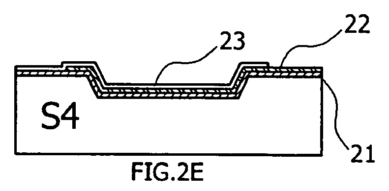
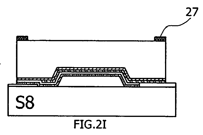
- FIGS. 2A to 2K are sectional views illustrating a process for fabricating a capacitive pressure sensor in accordance with the present invention; and
- FIGS. 3A and 3B are schematic sectional views illustrating the operation of the capacitive pressure sensor in accordance with the present invention.
- Now, a preferred embodiment of the present invention will be described in detail with reference to the annexed drawings.
- Hereinafter, a method for fabricating a capacitive pressure sensor having high linearity in accordance with the present invention will be described with reference to FIGS. 2A to 2K.
- First, as shown in FIGS. 2A to 2K, a
silicon substrate 20 is used to form amembrane 30, and aglass substrate 25 is used to form a bondingmetal pad electrode 26. - As shown in FIG. 2A, the
silicon substrate 20 is prepared. As shown in FIG. 2B, the front surface of thesilicon substrate 20 is etched to a designated depth in a first step (S1). Here, when anisotropic chemical etching using potassium hydroxide (KOH) or ethylene diamine pyrocatechol (EDP) is performed, silicon nitride (SixNy), silicon dioxide (SiO2), or metal, such as gold (Au) or chrome (Cr), is used as a mask material, or when dry etching is performed, photoresist, or metal, such as gold (Au), chrome (Cr), or aluminum (A1), is used as a mask material. - As shown in FIG. 2C, silicon dioxide (SiO2) is deposited on the etched surface of the
silicon substrate 20, thus forming anetching stopper 21 for stopping anisotropic chemical etching using potassium hydroxide (KOH) or ethylene diamine pyrocatechol (EDP), which will be later described in an eighth step (S8), in a second step (2). - As shown in FIG. 2D, doped polysilicon is deposited on the surface of the
etching stopper 21, thus forming anupper electrode 22 of a capacitor, in a third step (S3). Thereafter, as shown in FIG. 2E, in order to increase the sensitivity of the pressure sensor, hafnium oxide having excellent insulating properties and a high dielectric constant is deposited on the surface of theupper electrode 22, thus forming an insulatinglayer 23, in a fourth step (S4). Since the hafnium oxide has excellent insulating properties, the use of the insulatinglayer 23 with a small thickness increases the capacitance of thecapacitor 29. - As shown in FIG. 2F, doped polysilicon is deposited on the insulating
layer 23, thus forming alower electrode 24 of thecapacitor 29, in a fifth step (S5). Thereby, the formation of thecapacitor 29 is completed. - As shown in FIG. 2G, a
metal pad electrode 26 is formed on the front surface of theglass substrate 25 in a sixth step (S6). Thereafter, as shown in FIG. 2H, thelower electrode 24 of thecapacitor 29 of thesilicon substrate 20 and themetal pad electrode 26 of theglass substrate 25 are hybrid-bonded using an electric (anodic) bonding method in a seventh step (S7). - As shown in FIGS. 2I and 2J, in order to form the
capacitor 29, of thesilicon substrate 20 bonded to theglass substrate 25, in the shape of themembrane 30, the rear surface of thesilicon substrate 20 is etched by anisotropic chemical etching using potassium hydroxide (KOH) or ethylene diamine pyrocatechol (EDP), thus selectively exposing theetching stopper 21, in the eighth step (S8). Here, silicon nitride (SixNy), silicon dioxide (SiO2), or metal, such as gold (Au) or chrome (Cr), is used as a mask material, and silicon dioxide (SiO2) is used as theetching stopper 21. - Finally, as shown in FIG. 2K, the portion of the
etching stopper 21, which is exposed from the surface of thecapacitor 29 by the anisotropic chemical etching in the eighth step (S8), is removed by wet etching, and forming themembrane 30 having a three-layer structure, which moves according to a variation of pressure, in a ninth step (S9). Through the above steps, the fabrication of the capacitive pressure sensor of the present invention is completed. - The
membrane 30 having the above three-layer structure includes theupper electrode 22, the insulatinglayer 23, and thelower electrode 24. - FIGS. 3A and 3B are schematic sectional views illustrating the operation of the capacitive pressure sensor of the present invention, which is fabricated by the above method.
- When external pressure is not applied to the
membrane 30, themembrane 30 maintains its level state, as shown in FIG. 3A, and when external pressure is applied to themembrane 30, themembrane 30 is concavely bent into an arched state and thus has an increased area, as shown in FIG. 3B. Since the area of themembrane 30 means the area of the capacitor, the capacitance of the capacitor is changed. - The capacitance is in proportion to the area of the
membrane 30, and when external pressure is applied to themembrane 30, themembrane 30 is concavely bent from the level state into the arched state. Accordingly, a variation of capacitance according to a variation of pressure exhibits linearity. - As apparent from the above description, the present invention provides a method for fabricating a capacitive pressure sensor, which has an area changed according to a variation of external pressure so that output is linearly changed according to input, and uses hafnium oxide having a high dielectric constant as an insulating material to increase the capacitance and thus to increase the sensitivity, and a capacitive pressure sensor fabricated thereby, thus allowing the capacitive pressure sensor to have high linearity and sensitivity.
- Although the preferred embodiment of the present invention has been disclosed for illustrative purposes, those skilled in the art will appreciate that various modifications, additions and substitutions are possible, without departing from the scope and spirit of the invention as disclosed in the accompanying claims.
Claims (9)
- A method for fabricating a capacitive pressure sensor comprising:etching the front surface of a silicon substrate to a designated depth;depositing an etching stopper, for stopping etching of the rear surface of the silicon substrate, on the surface of the silicon substrate;depositing an upper electrode of a capacitor on the surface of the etching stopper;depositing an insulating surface of the capacitor on the surface of the upper electrode;depositing a lower electrode of the capacitor on the surface of the insulating surface to form the capacitor;forming a metal pad electrode on the front surface of a glass substrate;hybrid-bonding the lower electrode of the capacitor of the silicon substrate and the metal pad electrode of the glass substrate using an electric (anodic) bonding method;etching the rear surface of the silicon substrate bonded to the glass substrate to selectively expose the etching stopper and thus to form a membrane; andremoving the exposed region of the etching stopper by wet etching.
- The method according to claim 1, wherein, in the etching of the front surface of the silicon substrate, anisotropic chemical etching using potassium hydroxide (KOH) or ethylene diamine pyrocatechol (EDP) is performed and silicon nitride (SixNy), silicon dioxide (SiO2) or a metal, selected from the group consisting of gold (Au) and chrome (Cr), is used as a mask material.
- The method according to claim 1, wherein, in the etching of the front surface of the silicon substrate, dry etching is performed and photoresist or a metal, selected from the group consisting of gold (Au), chrome (Cr) and aluminum (A1), is used as a mask material.
- The method according to claim 1, wherein the etching stopper, for stopping the etching of the rear surface of the silicon substrate by anisotropic chemical etching using potassium hydroxide (KOH) or ethylene diamine pyrocatechol (EDP), is made of silicon dioxide (SiO2), in the depositing of the etching stopper.
- The method according to claim 1, wherein the upper electrode is made of doped polysilicon, in the depositing of the upper electrode of the capacitor.
- The method according to claim 1, wherein the insulating layer is made of hafnium oxide, in the depositing of the insulating layer of the capacitor.
- The method according to claim 1, wherein the lower electrode is made of doped polysilicon, in the depositing of the lower electrode.
- The method according to claim 1, wherein the rear surface of the silicon substrate is etched by anisotropic chemical etching, in the etching of the rear surface of the silicon substrate, and thus the capacitor is formed in the shape of the membrane having a three-layer structure moving according to a variation of pressure, in the removing of the exposed region of the etching stopper.
- A capacitive pressure sensor fabricated by the method according to any one of claims 1 to 8.
Applications Claiming Priority (1)
| Application Number | Priority Date | Filing Date | Title |
|---|---|---|---|
| KR1020060086897A KR100807193B1 (en) | 2006-09-08 | 2006-09-08 | Method of manufacturing capacitive pressure sensor and capacitive pressure sensor manufactured thereby |
Publications (1)
| Publication Number | Publication Date |
|---|---|
| EP1898196A2 true EP1898196A2 (en) | 2008-03-12 |
Family
ID=38800840
Family Applications (1)
| Application Number | Title | Priority Date | Filing Date |
|---|---|---|---|
| EP07002840A Withdrawn EP1898196A2 (en) | 2006-09-08 | 2007-02-09 | Method for fabricating capacitive pressure sensor and capacitive pressure sensor fabricated thereby |
Country Status (4)
| Country | Link |
|---|---|
| US (1) | US7571651B2 (en) |
| EP (1) | EP1898196A2 (en) |
| JP (1) | JP2008064734A (en) |
| KR (1) | KR100807193B1 (en) |
Cited By (1)
| Publication number | Priority date | Publication date | Assignee | Title |
|---|---|---|---|---|
| US10612991B1 (en) * | 2017-08-25 | 2020-04-07 | Fluke Corporation | High dynamic range capacitive pressure sensor |
Families Citing this family (14)
| Publication number | Priority date | Publication date | Assignee | Title |
|---|---|---|---|---|
| US8297125B2 (en) * | 2008-05-23 | 2012-10-30 | Honeywell International Inc. | Media isolated differential pressure sensor with cap |
| US8230745B2 (en) * | 2008-11-19 | 2012-07-31 | Honeywell International Inc. | Wet/wet differential pressure sensor based on microelectronic packaging process |
| US8322225B2 (en) * | 2009-07-10 | 2012-12-04 | Honeywell International Inc. | Sensor package assembly having an unconstrained sense die |
| JP5696045B2 (en) | 2009-07-24 | 2015-04-08 | ローム株式会社 | Semiconductor pressure sensor |
| KR101044914B1 (en) * | 2009-10-30 | 2011-06-28 | (주) 유니크코리아엔아이 | Capacitive pressure sensor with diffusion barrier |
| US8230743B2 (en) | 2010-08-23 | 2012-07-31 | Honeywell International Inc. | Pressure sensor |
| KR101248185B1 (en) * | 2011-02-23 | 2013-03-27 | 서강대학교산학협력단 | Pressure sensor having wireless charging module and method for manufacturing the same |
| US9596988B2 (en) | 2011-10-12 | 2017-03-21 | Purdue Research Foundation | Pressure sensors for small-scale applications and related methods |
| JP6008393B2 (en) | 2012-07-28 | 2016-10-19 | 株式会社ワコム | Electromagnetic induction type position indicator and electronic ink cartridge |
| JP6012069B2 (en) * | 2012-09-13 | 2016-10-25 | 株式会社ワコム | Electromagnetic induction type position indicator and electronic ink cartridge |
| CN108375446B (en) * | 2018-04-17 | 2023-04-28 | 南京信息工程大学 | A sounding giant piezoresistive air pressure sensor array device and measurement method |
| CN117268624B (en) * | 2023-09-22 | 2026-04-17 | 深圳安培龙科技股份有限公司 | A silicon piezoresistive pressure sensor chip and its fabrication method |
| KR102781001B1 (en) | 2023-11-21 | 2025-03-19 | 어보브반도체 주식회사 | Device And Method For Detecting Pressure Touch With Improved Structure |
| CN117923411B (en) * | 2024-03-25 | 2024-07-12 | 成都凯天电子股份有限公司 | A method for preparing a silicon carbide capacitive pressure sensor |
Family Cites Families (5)
| Publication number | Priority date | Publication date | Assignee | Title |
|---|---|---|---|---|
| US4998179A (en) * | 1989-02-28 | 1991-03-05 | United Technologies Corporation | Capacitive semiconductive sensor with hinged diaphragm for planar movement |
| JPH07243929A (en) * | 1994-03-07 | 1995-09-19 | Hokuriku Electric Ind Co Ltd | Electrostatic capacity type pressure sensor |
| KR19980078153A (en) * | 1997-04-25 | 1998-11-16 | 김영환 | Silicon Capacitive Pressure Sensor |
| JP2005032991A (en) * | 2003-07-14 | 2005-02-03 | Renesas Technology Corp | Semiconductor device |
| JP2007036126A (en) * | 2005-07-29 | 2007-02-08 | Fujitsu Ltd | Semiconductor device and manufacturing method thereof |
-
2006
- 2006-09-08 KR KR1020060086897A patent/KR100807193B1/en not_active Expired - Fee Related
-
2007
- 2007-02-03 US US11/702,149 patent/US7571651B2/en not_active Expired - Fee Related
- 2007-02-09 EP EP07002840A patent/EP1898196A2/en not_active Withdrawn
- 2007-02-15 JP JP2007034290A patent/JP2008064734A/en active Pending
Cited By (2)
| Publication number | Priority date | Publication date | Assignee | Title |
|---|---|---|---|---|
| US10612991B1 (en) * | 2017-08-25 | 2020-04-07 | Fluke Corporation | High dynamic range capacitive pressure sensor |
| US11248975B2 (en) | 2017-08-25 | 2022-02-15 | Fluke Corporation | High dynamic range capacitive pressure sensor |
Also Published As
| Publication number | Publication date |
|---|---|
| JP2008064734A (en) | 2008-03-21 |
| KR100807193B1 (en) | 2008-02-28 |
| US20080061799A1 (en) | 2008-03-13 |
| US7571651B2 (en) | 2009-08-11 |
Similar Documents
| Publication | Publication Date | Title |
|---|---|---|
| US7571651B2 (en) | Capacitive pressure sensor and method for fabricating the same | |
| US7563692B2 (en) | Microelectromechanical system pressure sensor and method for making and using | |
| KR100404904B1 (en) | A capacitive differential pressure sensor and method for manufacturing thereof | |
| US7114397B2 (en) | Microelectromechanical system pressure sensor and method for making and using | |
| JPH10135487A (en) | Integrated piezoresistive pressure sensor and method of manufacturing the same | |
| CN206164826U (en) | Sensitive membrane and MEMS microphone | |
| US8754453B2 (en) | Capacitive pressure sensor and method for manufacturing same | |
| IE20110548A1 (en) | A method for fabricating a sensor | |
| CN111811726B (en) | Micromechanical components for capacitive sensors or switching devices | |
| CN101661012A (en) | Microfilm capacitive type surface stress sensor used for biochemical detection and manufacture method thereof | |
| CN104502003A (en) | Silica glass mosaic structure micromachine differential capacitance type pressure gauge | |
| CN104062044A (en) | Micro mechanical differential capacitive pressure gauge | |
| CN110482475A (en) | A kind of capacitance pressure transducer, based on MEMS | |
| CN113758613A (en) | SOI-based resistance center placed piezoresistive pressure sensor | |
| CN113670485A (en) | High-performance MEMS pressure sensor and manufacturing method thereof | |
| CN112683348B (en) | MEMS capacitive flow sensor and preparation method thereof | |
| CN115452207A (en) | Differential capacitance type MEMS pressure sensor and manufacturing method thereof | |
| CN114671399A (en) | Capacitive pressure sensor and preparation method thereof | |
| US12623899B2 (en) | Absolute pressure sensing MEMS microphone, microphone unit and electronic device | |
| CN103180705A (en) | Microelectromechanical sensor for measuring force and corresponding method | |
| CN217520622U (en) | Capacitive sensitive chip structure with vertically arranged polar plates | |
| JP2012063363A (en) | Pressure sensor | |
| Park et al. | A capacitive absolute-pressure sensor with external pick-off electrodes | |
| JPH1183658A (en) | Capacitive sensor | |
| Ferrari et al. | Printed thick-film capacitive sensors |
Legal Events
| Date | Code | Title | Description |
|---|---|---|---|
| PUAI | Public reference made under article 153(3) epc to a published international application that has entered the european phase |
Free format text: ORIGINAL CODE: 0009012 |
|
| AK | Designated contracting states |
Kind code of ref document: A2 Designated state(s): AT BE BG CH CY CZ DE DK EE ES FI FR GB GR HU IE IS IT LI LT LU LV MC NL PL PT RO SE SI SK TR |
|
| AX | Request for extension of the european patent |
Extension state: AL BA HR MK YU |
|
| STAA | Information on the status of an ep patent application or granted ep patent |
Free format text: STATUS: THE APPLICATION HAS BEEN WITHDRAWN |
|
| 18W | Application withdrawn |
Effective date: 20100329 |