EP1895572A2 - Bonded wafer and method for producing bonded wafer - Google Patents
Bonded wafer and method for producing bonded wafer Download PDFInfo
- Publication number
- EP1895572A2 EP1895572A2 EP07016998A EP07016998A EP1895572A2 EP 1895572 A2 EP1895572 A2 EP 1895572A2 EP 07016998 A EP07016998 A EP 07016998A EP 07016998 A EP07016998 A EP 07016998A EP 1895572 A2 EP1895572 A2 EP 1895572A2
- Authority
- EP
- European Patent Office
- Prior art keywords
- silicon wafer
- active layer
- wafer
- bonded
- support substrate
- Prior art date
- Legal status (The legal status is an assumption and is not a legal conclusion. Google has not performed a legal analysis and makes no representation as to the accuracy of the status listed.)
- Granted
Links
Images

Classifications
-
- H—ELECTRICITY
- H10—SEMICONDUCTOR DEVICES; ELECTRIC SOLID-STATE DEVICES NOT OTHERWISE PROVIDED FOR
- H10P—GENERIC PROCESSES OR APPARATUS FOR THE MANUFACTURE OR TREATMENT OF DEVICES COVERED BY CLASS H10
- H10P95/00—Generic processes or apparatus for manufacture or treatments not covered by the other groups of this subclass
-
- H—ELECTRICITY
- H10—SEMICONDUCTOR DEVICES; ELECTRIC SOLID-STATE DEVICES NOT OTHERWISE PROVIDED FOR
- H10P—GENERIC PROCESSES OR APPARATUS FOR THE MANUFACTURE OR TREATMENT OF DEVICES COVERED BY CLASS H10
- H10P10/00—Bonding of wafers, substrates or parts of devices
- H10P10/12—Bonding of semiconductor wafers or semiconductor substrates to semiconductor wafers or semiconductor substrates
- H10P10/128—Bonding of semiconductor wafers or semiconductor substrates to semiconductor wafers or semiconductor substrates by direct semiconductor to semiconductor bonding
-
- H—ELECTRICITY
- H10—SEMICONDUCTOR DEVICES; ELECTRIC SOLID-STATE DEVICES NOT OTHERWISE PROVIDED FOR
- H10D—INORGANIC ELECTRIC SEMICONDUCTOR DEVICES
- H10D86/00—Integrated devices formed in or on insulating or conducting substrates, e.g. formed in silicon-on-insulator [SOI] substrates or on stainless steel or glass substrates
-
- H—ELECTRICITY
- H10—SEMICONDUCTOR DEVICES; ELECTRIC SOLID-STATE DEVICES NOT OTHERWISE PROVIDED FOR
- H10P—GENERIC PROCESSES OR APPARATUS FOR THE MANUFACTURE OR TREATMENT OF DEVICES COVERED BY CLASS H10
- H10P52/00—Grinding, lapping or polishing of wafers, substrates or parts of devices
Definitions
- This invention relates to a bonded wafer and a method for producing a bonded wafer, and more particularly it is to suppress residual oxide in a bonded face as far as possible.
- a method wherein two silicon wafers are bonded through an insulating film such as an oxide film or the like or directly bonded without the insulating film and then a wafer for active layer is grinded and polished to form an active layer (grind-polishing method), and a method wherein ions of hydrogen or the like are implanted into a surface layer portion of a silicon wafer for active layer to form an ion-implanted layer and bonded to a silicon wafer for support substrate and then subjected to a heat treatment to exfoliate the wafer at the ion-implanted layer to thereby form an active layer (ion implanting separation method) or so-called smart cut method (registered trade mark) (see JP-A-H11-67701 and JP-AH05-211128 ).
- an object of the invention to advantageously solve the above problems and to provide a method for producing a bonded wafer wherein the retaining of the oxide in the interface can be effectively removed when the two silicon wafers are directly bonded without the insulating film as well as a
- the inventors have made various studies in order to solve the above problems and obtained the following knowledge. That is, when wafers to be bonded are cut out from an ingot, it is common that the cutting angle is not more than 1° in both of X-axis and Y-axis. However, it has been found that the retaining of the step-like oxide in the bonded interface can be effectively removed by strictly controlling the cutting angle from the ingot to a range of 0-0.1° (compound angle) with respect to a predetermined crystal face, and as a result the invention has been accomplished.
- a method for producing a bonded wafer by directly bonding a silicon wafer for active layer and a silicon wafer for support substrate without an insulating film and thinning the silicon wafer for active layer to a given thickness characterized in that a silicon wafer cut out from an ingot at a cutting angle of 0-0.1 (compound angle) with respect to a predetermined crystal face is used in each of the said silicon wafer for active layer and silicon wafer for support substrate.
- a bonded wafer obtained by directly bonding a silicon wafer for active layer and a silicon wafer for support substrate without an insulating film and thinning the silicon wafer for active layer to a given thickness characterized in that a silicon wafer cut out from an ingot at a cutting angle of 0-0.1° (compound angle) with respect to a predetermined crystal face is used in each of the said silicon wafer for active layer and silicon wafer for support substrate.
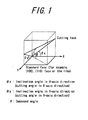
- FIG. 1 is a schematic illustration of cutting angle and compound angle.
- FIG. 2 is TEM photographs (a) and (b) of bonded interfaces of Example 1 and Comparative Example 1, respectively.
- the cutting angle is controlled to a range of 0-0.1° (compound angle) with respect to a predetermined crystal face (which is also called as a standard face).
- a predetermined crystal face which is also called as a standard face.
- cutting angle means an angle of the cut face with respect to X-axis or Y-axis of the standard face as shown in FIG. 1, while the compound angle ⁇ compounding an inclination angle ⁇ x of the standard face in X-axis direction (cutting angle in X-axis direction) and an inclination angle ⁇ y of the standard face in Y-axis direction (cutting angle in Y-axis direction).
- the compound angle of each of the two silicon wafers to be bonded is 0-0.1° because the remnant of the oxide
- the remnant of step-like oxide in the bonded interface can be largely reduced by controlling the cutting angle of each of the two silicon wafers from the ingot to a range of 0-0.1° (compound angle) according to the invention, the inventors have guessed as follows. In the bonded interface, it seems that oxides are formed on the face of the wafer to be bonded and aggregated in the bonded interface and finally retain as step-like oxide. Therefore, it is considered that the remnant of the step-like oxide in the bonded interface can be suppressed by bonding silicon wafers each having a cut face substantially parallel to the standard face of the crystal.
- the surface of the wafer is rendered into a hydrophobic face by cleaning the wafer surface to remove native oxide film or the like before the bonding of the wafers.
- hydrophobic face used herein means a clean face having no oxide film and the like.
- the cleaning method is not particularly limited, and can utilize the conventionally well-known method of cleaning in HF solution and the like.
- the invention is effective to the direct bonding of silicon wafers having different crystal orientations, for example, the direct bonding of (110) crystal and (100) crystal.
- an ion implantation-separation process with hydrogen gas or the like can be utilized as a method of thinning the wafer for active layer.
- This ion implantation-separation process is a method wherein a rare gas such as hydrogen gas or the like is implanted into the silicon wafer for active layer from its bonding face to form an ion implanted layer before the bonding and then the silicon wafer for active layer is bonded to the silicon wafer for support substrate and subjected to a heat treatment at about 500°C to exfoliate a part of the wafer for active layer bounding the ion implanted layer.
- a silicon wafer for active layer is cut at a compound angle of 0.07° with respect to (100) face as a standard face, and a silicon wafer for support substrate is cut at a compound angle of 0.07°.
- the thus obtained two silicon wafers are immersed in a HF cleaning solution to completely remove a native oxide film and directly bonded to each other and subjected to a heat treatment at 1100°C for 120 minutes for further improving the bonding strength.
- the wafer for active layer is ground and polished so as to render the thickness of the active layer into 100 nm.
- An oxide existing in an interface of the thus obtained bonded wafer is observed by a plane TEM (transmission electron microscopy). The measured result is shown in Table 1 and FIG. 2(a).
- a silicon wafer for active layer is cut at a compound angle of 0.07° with respect to (100) face as a standard face, and a silicon wafer for support substrate is cut at a compound angle of 0.07°.
- hydrogen ions are implanted into the voltage: 50 keV and a dose: 1x10 17 atoms/cm 2 to form a hydrogen ion implanted layer at a depth position of about 500 nm from the surface of the wafer for active layer.
- the silicon wafers for active layer and for support substrate are immersed in HF cleaning solution to completely remove a native oxide film and directly bonded to each other and subjected to a heat treatment at 500°C to exfoliate a part of the bonded wafer bounding the hydrogen ion implanted layer.
- the bonded wafer is subjected to a heat treatment at 1100°C for 120 minutes for further improving the bonding strength and further to an oxidation treatment to thin the thickness of the active layer to 100 nm.
- An oxide existing in an interface of the thus obtained bonded wafer is observed by the plane TEM. The measured result is shown in Table 1.
- Example 1 the step-like oxide can not be observed likewise Example 1.
- a bonded wafer is prepared in the same manner as in Example 1 except that the compound angle of the silicon wafer for active layer is 0.12° and the compound angle of the silicon wafer for support substrate is 0.12°.
- An oxide existing in an interface of the thus obtained bonded wafer is observed by the plane TEM to obtain a result as shown in Table 1 and FIG. 2(b).
- a bonded wafer is prepared in the same manner as in Example 2 except that the compound angle of the silicon wafer for active layer is 0.12° and the compound angle of the silicon wafer for support substrate is 0.12°.
- An oxide existing in an interface of the thus obtained bonded wafer is observed by the plane TEM to obtain a result as shown in Table 1.
Landscapes
- Crystals, And After-Treatments Of Crystals (AREA)
- Mechanical Treatment Of Semiconductor (AREA)
- Element Separation (AREA)
- Recrystallisation Techniques (AREA)
Abstract
Description
- This invention relates to a bonded wafer and a method for producing a bonded wafer, and more particularly it is to suppress residual oxide in a bonded face as far as possible.
- As a typical production method of a bonded wafer, there are known a method wherein two silicon wafers are bonded through an insulating film such as an oxide film or the like or directly bonded without the insulating film and then a wafer for active layer is grinded and polished to form an active layer (grind-polishing method), and a method wherein ions of hydrogen or the like are implanted into a surface layer portion of a silicon wafer for active layer to form an ion-implanted layer and bonded to a silicon wafer for support substrate and then subjected to a heat treatment to exfoliate the wafer at the ion-implanted layer to thereby form an active layer (ion implanting separation method) or so-called smart cut method (registered trade mark) (see
JP-A-H11-67701 JP-AH05-211128 - However, when the two silicon wafers are directly bonded after the removal of a native oxide by immersing in a HF solution, or particularly when two silicon wafers having different crystal orientations (for example, (110) face and (100) face) are directly bonded without using an insulating film such as an oxide film or the like, an oxide trapped in an interface therebetween may locally concentrate and retain in the interface as a step-like oxide in the production step of the bonded wafer (heat treatment step). As a result, there is a problem that such a residual oxide deteriorates the device characteristics but also forms a nucleus of defect in the preparation step of the device.
- It is, therefore, an object of the invention to advantageously solve the above problems and to provide a method for producing a bonded wafer wherein the retaining of the oxide in the interface can be effectively removed when the two silicon wafers are directly bonded without the insulating film as well as a
- There will be described the development of the invention below. That is, when two silicon wafers are directly bonded without an insulating film, it is considered that an oxide retaining in a bonded interface is formed by condensing the oxide trapped in the bonded interface. In order to prevent the retaining of such an oxide, therefore, the bonding is usually conducted after the wafers are cleaned with a HF solution to remove a native oxide from the surface of the wafer.
Even when the surface of the wafer is cleaned with the HF solution or the like prior to the bonding, however, the step-like oxide may be retained in the bonded interface. - The inventors have made various studies in order to solve the above problems and obtained the following knowledge.
That is, when wafers to be bonded are cut out from an ingot, it is common that the cutting angle is not more than 1° in both of X-axis and Y-axis. However, it has been found that the retaining of the step-like oxide in the bonded interface can be effectively removed by strictly controlling the cutting angle from the ingot to a range of 0-0.1° (compound angle) with respect to a predetermined crystal face, and as a result the invention has been accomplished. - That is, the summary and construction of the invention are as follows.
1. A method for producing a bonded wafer by directly bonding a silicon wafer for active layer and a silicon wafer for support substrate without an insulating film and thinning the silicon wafer for active layer to a given thickness, characterized in that a silicon wafer cut out from an ingot at a cutting angle of 0-0.1 (compound angle) with respect to a predetermined crystal face is used in each of the said silicon wafer for active layer and silicon wafer for support substrate. - 2. A method for producing a bonded wafer according to item 1, wherein the silicon wafers for active layer and for support substrate are bonded at a state of hydrophobic face.
- 3. A method for producing a bonded wafer according to item 1, wherein wafers having different crystal orientations are used as the silicon wafers for active layer and for support substrate.
wherein the thinning of the silicon wafer for active layer is carried out by an ion implantation-separation process. - 5. A bonded wafer obtained by directly bonding a silicon wafer for active layer and a silicon wafer for support substrate without an insulating film and thinning the silicon wafer for active layer to a given thickness, characterized in that a silicon wafer cut out from an ingot at a cutting angle of 0-0.1° (compound angle) with respect to a predetermined crystal face is used in each of the said silicon wafer for active layer and silicon wafer for support substrate.
- According to the invention, there cane be largely reduced the remnant of step-like oxide, which has been feared when the two silicon wafers are directly bonded without the insulating film.
- FIG. 1 is a schematic illustration of cutting angle and compound angle.
FIG. 2 is TEM photographs (a) and (b) of bonded interfaces of Example 1 and Comparative Example 1, respectively. - The invention will be described in detail with reference to the accompanying drawings below.
- In the invention, it is important that when a silicon wafer is cut out from an ingot, the cutting angle is controlled to a range of 0-0.1° (compound angle) with respect to a predetermined crystal face (which is also called as a standard face). When the cutting angle (compound angle) exceeds 0.1°, the step-like oxide retains in the bonded interface, which badly affects the preparation step of the device and properties thereof.
- The term "cutting angle" used herein means an angle of the cut face with respect to X-axis or Y-axis of the standard face as shown in FIG. 1, while the compound angle θ compounding an inclination angle θx of the standard face in X-axis direction (cutting angle in X-axis direction) and an inclination angle θy of the standard face in Y-axis direction (cutting angle in Y-axis direction).
- In the invention, it is also important that the compound angle of each of the two silicon wafers to be bonded is 0-0.1° because the remnant of the oxide
- Although it is not yet clearly elucidated that the remnant of step-like oxide in the bonded interface can be largely reduced by controlling the cutting angle of each of the two silicon wafers from the ingot to a range of 0-0.1° (compound angle) according to the invention, the inventors have guessed as follows.
In the bonded interface, it seems that oxides are formed on the face of the wafer to be bonded and aggregated in the bonded interface and finally retain as step-like oxide. Therefore, it is considered that the remnant of the step-like oxide in the bonded interface can be suppressed by bonding silicon wafers each having a cut face substantially parallel to the standard face of the crystal. - In the bonding of the two silicon wafers, it is required to clean the surface of the wafer as far as possible. In the invention, it is advantageous that the surface of the wafer is rendered into a hydrophobic face by cleaning the wafer surface to remove native oxide film or the like before the bonding of the wafers. The term "hydrophobic face" used herein means a clean face having no oxide film and the like. Also, the cleaning method is not particularly limited, and can utilize the conventionally well-known method of cleaning in HF solution and the like.
- Moreover, the invention is effective to the direct bonding of silicon wafers having different crystal orientations, for example, the direct bonding of (110) crystal and (100) crystal.
- In the invention, an ion implantation-separation process with hydrogen gas or the like can be utilized as a method of thinning the wafer for active layer. This ion implantation-separation process is a method wherein a rare gas such as hydrogen gas or the like is implanted into the silicon wafer for active layer from its bonding face to form an ion implanted layer before the bonding and then the silicon wafer for active layer is bonded to the silicon wafer for support substrate and subjected to a heat treatment at about 500°C to exfoliate a part of the wafer for active layer bounding the ion implanted layer. By using the ion implantation-separation process can be uniformly thinned the active layer without using a grinding, a polishing or an etching.
- When a silicon wafer is cut out from a silicon ingot grown by CZ method, a silicon wafer for active layer is cut at a compound angle of 0.07° with respect to (100) face as a standard face, and a silicon wafer for support substrate is cut at a compound angle of 0.07°. The thus obtained two silicon wafers are immersed in a HF cleaning solution to completely remove a native oxide film and directly bonded to each other and subjected to a heat treatment at 1100°C for 120 minutes for further improving the bonding strength. Then, the wafer for active layer is ground and polished so as to render the thickness of the active layer into 100 nm.
An oxide existing in an interface of the thus obtained bonded wafer is observed by a plane TEM (transmission electron microscopy).
The measured result is shown in Table 1 and FIG. 2(a). -
Table 1 Compound angle of wafer for active layer (°) Compound angle of wafer for support substrate (°) Step-like oxide Example 1 0.07 0.07 none Example 2 0.07 0.07 none Comparative Example 1 0.12 0.12 presence Comparative Example 2 0.12 0.12 presence - As seen from Table 1 and FIG. 2(a), in case of using the silicon wafers cut out from the ingot according to the invention, the remnant of the step-like oxide is not observed.
- When a silicon wafer is cut out from a silicon ingot grown by CZ method, a silicon wafer for active layer is cut at a compound angle of 0.07° with respect to (100) face as a standard face, and a silicon wafer for support substrate is cut at a compound angle of 0.07°. Then, hydrogen ions are implanted into the voltage: 50 keV and a dose: 1x10¹⁷ atoms/cm2 to form a hydrogen ion implanted layer at a depth position of about 500 nm from the surface of the wafer for active layer.
Then, the silicon wafers for active layer and for support substrate are immersed in HF cleaning solution to completely remove a native oxide film and directly bonded to each other and subjected to a heat treatment at 500°C to exfoliate a part of the bonded wafer bounding the hydrogen ion implanted layer.
Next, the bonded wafer is subjected to a heat treatment at 1100°C for 120 minutes for further improving the bonding strength and further to an oxidation treatment to thin the thickness of the active layer to 100 nm.
An oxide existing in an interface of the thus obtained bonded wafer is observed by the plane TEM.
The measured result is shown in Table 1. - In this case, the step-like oxide can not be observed likewise Example 1.
- A bonded wafer is prepared in the same manner as in Example 1 except that the compound angle of the silicon wafer for active layer is 0.12° and the compound angle of the silicon wafer for support substrate is 0.12°.
An oxide existing in an interface of the thus obtained bonded wafer is observed by the plane TEM to obtain a result as shown in Table 1 and FIG. 2(b). - As seen from Table 1 and FIG. 2(b), when the cutting angle of the silicon wafer is outside the acceptable range of the invention, the remnant of the step-like oxide is observed at the bonded interface.
- A bonded wafer is prepared in the same manner as in Example 2 except that the compound angle of the silicon wafer for active layer is 0.12° and the compound angle of the silicon wafer for support substrate is 0.12°.
An oxide existing in an interface of the thus obtained bonded wafer is observed by the plane TEM to obtain a result as shown in Table 1. - As seen from Table, the remnant of the step-like oxide is also observed likewise Comparative Example 1.
Claims (5)
- A method for producing a bonded wafer by directly bonding a silicon wafer for active layer and a silicon wafer for support substrate without an insulating film and thinning the silicon wafer for active layer to a given thickness, characterized in that a silicon wafer cut out from an ingot at a cutting angle of 0-0.1°(compound angle) with respect to a predetermined crystal face is used in each of the said silicon wafer for active layer and silicon wafer for support substrate.
- A method for producing a bonded wafer according to claim 1, wherein the silicon wafers for active layer and for support substrate are bonded at a state of hydrophobic face.
- A method for producing a bonded wafer according to claim 1 or 2, wherein wafers having different crystal orientations are used as the silicon wafers for active layer and for support substrate.
- A method for producing a bonded wafer according to any one of claims 1-3, wherein the thinning of the silicon wafer for active layer is carried out by an ion implantation-separation process.
- A bonded wafer obtained by directly bonding a silicon wafer for active layer and a silicon wafer for support substrate without an insulating film and thinning the silicon wafer for active layer to a given thickness, characterized in that a silicon wafer cut out from an ingot at a cutting angle of 0-0.1° (compound angle) with respect to a predetermined crystal face is used in each of the said silicon wafer for active layer and silicon wafer for support substrate.
Applications Claiming Priority (1)
| Application Number | Priority Date | Filing Date | Title |
|---|---|---|---|
| JP2006235919A JP2008060355A (en) | 2006-08-31 | 2006-08-31 | Bonded wafer manufacturing method and bonded wafer |
Publications (3)
| Publication Number | Publication Date |
|---|---|
| EP1895572A2 true EP1895572A2 (en) | 2008-03-05 |
| EP1895572A3 EP1895572A3 (en) | 2009-04-15 |
| EP1895572B1 EP1895572B1 (en) | 2011-02-09 |
Family
ID=38566821
Family Applications (1)
| Application Number | Title | Priority Date | Filing Date |
|---|---|---|---|
| EP07016998A Ceased EP1895572B1 (en) | 2006-08-31 | 2007-08-30 | Method for producing bonded wafer |
Country Status (6)
| Country | Link |
|---|---|
| US (1) | US8048767B2 (en) |
| EP (1) | EP1895572B1 (en) |
| JP (1) | JP2008060355A (en) |
| KR (1) | KR100898534B1 (en) |
| CN (1) | CN101188194B (en) |
| SG (1) | SG140581A1 (en) |
Families Citing this family (2)
| Publication number | Priority date | Publication date | Assignee | Title |
|---|---|---|---|---|
| JP5555995B2 (en) * | 2008-09-12 | 2014-07-23 | 株式会社Sumco | Method for manufacturing bonded silicon wafer |
| CN115148850B (en) * | 2022-06-27 | 2023-06-02 | 晶科能源股份有限公司 | Silicon wafer, preparation method thereof and passivation treatment solution |
Citations (2)
| Publication number | Priority date | Publication date | Assignee | Title |
|---|---|---|---|---|
| JPH05211128A (en) | 1991-09-18 | 1993-08-20 | Commiss Energ Atom | Method for manufacturing thin semiconductor material film |
| JPH11167701A (en) | 1997-12-03 | 1999-06-22 | Toshiba Corp | Disk apparatus and data recording order control method applied to the apparatus |
Family Cites Families (17)
| Publication number | Priority date | Publication date | Assignee | Title |
|---|---|---|---|---|
| JPH0691147B2 (en) * | 1988-10-14 | 1994-11-14 | 信越半導体株式会社 | Bonding wafer inspection method |
| US5451547A (en) * | 1991-08-26 | 1995-09-19 | Nippondenso Co., Ltd. | Method of manufacturing semiconductor substrate |
| JP3175323B2 (en) * | 1991-08-26 | 2001-06-11 | 株式会社デンソー | Semiconductor substrate manufacturing method |
| US5152842A (en) * | 1991-12-05 | 1992-10-06 | Rohm Co., Ltd. | Reactor for epitaxial growth |
| DE19611043B4 (en) * | 1995-03-20 | 2006-02-16 | Toshiba Ceramics Co., Ltd. | A method of producing a silicon wafer, a method of forming a silicon wafer, and a method of manufacturing a semiconductor device |
| FR2766620B1 (en) * | 1997-07-22 | 2000-12-01 | Commissariat Energie Atomique | PRODUCTION OF MICROSTRUCTURES OR NANOSTRUCTURES ON A SUPPORT |
| JP3216583B2 (en) * | 1997-08-22 | 2001-10-09 | 住友金属工業株式会社 | Manufacturing method of bonded SOI substrate |
| JP3223873B2 (en) * | 1997-12-24 | 2001-10-29 | 住友金属工業株式会社 | Silicon wafer and method for manufacturing the same |
| JP4603677B2 (en) * | 2000-11-09 | 2010-12-22 | 信越半導体株式会社 | Annealed wafer manufacturing method and annealed wafer |
| FR2819099B1 (en) * | 2000-12-28 | 2003-09-26 | Commissariat Energie Atomique | METHOD FOR PRODUCING A STACKED STRUCTURE |
| US7153757B2 (en) * | 2002-08-29 | 2006-12-26 | Analog Devices, Inc. | Method for direct bonding two silicon wafers for minimising interfacial oxide and stresses at the bond interface, and an SOI structure |
| JP4190906B2 (en) * | 2003-02-07 | 2008-12-03 | 信越半導体株式会社 | Silicon semiconductor substrate and manufacturing method thereof |
| US20050217560A1 (en) * | 2004-03-31 | 2005-10-06 | Tolchinsky Peter G | Semiconductor wafers with non-standard crystal orientations and methods of manufacturing the same |
| JP4830290B2 (en) * | 2004-11-30 | 2011-12-07 | 信越半導体株式会社 | Manufacturing method of directly bonded wafer |
| US8138061B2 (en) * | 2005-01-07 | 2012-03-20 | International Business Machines Corporation | Quasi-hydrophobic Si-Si wafer bonding using hydrophilic Si surfaces and dissolution of interfacial bonding oxide |
| US20070215984A1 (en) * | 2006-03-15 | 2007-09-20 | Shaheen Mohamad A | Formation of a multiple crystal orientation substrate |
| US20080164572A1 (en) * | 2006-12-21 | 2008-07-10 | Covalent Materials Corporation | Semiconductor substrate and manufacturing method thereof |
-
2006
- 2006-08-31 JP JP2006235919A patent/JP2008060355A/en active Pending
-
2007
- 2007-08-30 EP EP07016998A patent/EP1895572B1/en not_active Ceased
- 2007-08-31 KR KR1020070088143A patent/KR100898534B1/en not_active Expired - Fee Related
- 2007-08-31 US US11/849,058 patent/US8048767B2/en active Active
- 2007-08-31 SG SG200706415-7A patent/SG140581A1/en unknown
- 2007-08-31 CN CN2007101821320A patent/CN101188194B/en not_active Expired - Fee Related
Patent Citations (2)
| Publication number | Priority date | Publication date | Assignee | Title |
|---|---|---|---|---|
| JPH05211128A (en) | 1991-09-18 | 1993-08-20 | Commiss Energ Atom | Method for manufacturing thin semiconductor material film |
| JPH11167701A (en) | 1997-12-03 | 1999-06-22 | Toshiba Corp | Disk apparatus and data recording order control method applied to the apparatus |
Also Published As
| Publication number | Publication date |
|---|---|
| JP2008060355A (en) | 2008-03-13 |
| CN101188194A (en) | 2008-05-28 |
| KR100898534B1 (en) | 2009-05-20 |
| US8048767B2 (en) | 2011-11-01 |
| EP1895572A3 (en) | 2009-04-15 |
| SG140581A1 (en) | 2008-03-28 |
| KR20080020578A (en) | 2008-03-05 |
| US20080057676A1 (en) | 2008-03-06 |
| EP1895572B1 (en) | 2011-02-09 |
| CN101188194B (en) | 2010-06-23 |
Similar Documents
| Publication | Publication Date | Title |
|---|---|---|
| US7867877B2 (en) | Method for manufacturing SOI wafer | |
| EP1453096B1 (en) | Method for producing a bonded wafer | |
| US7855129B2 (en) | Method for manufacturing direct bonded SOI wafer and direct bonded SOI wafer manufactured by the method | |
| US7767549B2 (en) | Method of manufacturing bonded wafer | |
| EP3358600B1 (en) | Method for producing bonded soi wafer | |
| EP2151851B1 (en) | Method for forming silicon oxide film of soi wafer | |
| KR101142138B1 (en) | Multilayer Substrate Cleaning Method, Substrate Bonding Method, And Bonded Wafer Manufacturing Method | |
| KR100947815B1 (en) | Manufacturing Method of SOI Wafer and SOI Wafer | |
| EP2402983B1 (en) | Method for manufacturing soi wafer | |
| JP2002305292A (en) | SOI wafer and manufacturing method thereof | |
| US7855132B2 (en) | Method of manufacturing bonded wafer | |
| EP2924736B1 (en) | Method for manufacturing soi wafer | |
| US20080061452A1 (en) | Bonded wafer and method of manufacturing the same | |
| EP1791175A2 (en) | Method of manufacturing bonded wafer | |
| EP1895572B1 (en) | Method for producing bonded wafer | |
| EP3007204B1 (en) | Method for manufacturing bonded wafer | |
| TW200300575A (en) | Manufacturing method of bonding wafer | |
| JP5541136B2 (en) | Method for manufacturing bonded SOI wafer | |
| EP1624488B1 (en) | An soi wafer and a method of producing the same | |
| US7902043B2 (en) | Method of producing bonded wafer | |
| US20110065258A1 (en) | Method of producing bonded substrate | |
| EP1939927B1 (en) | Method of manufacturing a bonded wafer | |
| US7510949B2 (en) | Methods for producing a multilayer semiconductor structure | |
| JP5555995B2 (en) | Method for manufacturing bonded silicon wafer |
Legal Events
| Date | Code | Title | Description |
|---|---|---|---|
| PUAI | Public reference made under article 153(3) epc to a published international application that has entered the european phase |
Free format text: ORIGINAL CODE: 0009012 |
|
| 17P | Request for examination filed |
Effective date: 20070830 |
|
| AK | Designated contracting states |
Kind code of ref document: A2 Designated state(s): AT BE BG CH CY CZ DE DK EE ES FI FR GB GR HU IE IS IT LI LT LU LV MC MT NL PL PT RO SE SI SK TR |
|
| AX | Request for extension of the european patent |
Extension state: AL BA HR MK YU |
|
| PUAL | Search report despatched |
Free format text: ORIGINAL CODE: 0009013 |
|
| AK | Designated contracting states |
Kind code of ref document: A3 Designated state(s): AT BE BG CH CY CZ DE DK EE ES FI FR GB GR HU IE IS IT LI LT LU LV MC MT NL PL PT RO SE SI SK TR |
|
| AX | Request for extension of the european patent |
Extension state: AL BA HR MK RS |
|
| 17Q | First examination report despatched |
Effective date: 20090803 |
|
| AKX | Designation fees paid |
Designated state(s): FR |
|
| REG | Reference to a national code |
Ref country code: DE Ref legal event code: 8566 |
|
| GRAP | Despatch of communication of intention to grant a patent |
Free format text: ORIGINAL CODE: EPIDOSNIGR1 |
|
| RTI1 | Title (correction) |
Free format text: METHOD FOR PRODUCING BONDED WAFER |
|
| GRAS | Grant fee paid |
Free format text: ORIGINAL CODE: EPIDOSNIGR3 |
|
| GRAA | (expected) grant |
Free format text: ORIGINAL CODE: 0009210 |
|
| AK | Designated contracting states |
Kind code of ref document: B1 Designated state(s): FR |
|
| PLBE | No opposition filed within time limit |
Free format text: ORIGINAL CODE: 0009261 |
|
| STAA | Information on the status of an ep patent application or granted ep patent |
Free format text: STATUS: NO OPPOSITION FILED WITHIN TIME LIMIT |
|
| 26N | No opposition filed |
Effective date: 20111110 |
|
| REG | Reference to a national code |
Ref country code: FR Ref legal event code: PLFP Year of fee payment: 10 |
|
| REG | Reference to a national code |
Ref country code: FR Ref legal event code: PLFP Year of fee payment: 11 |
|
| REG | Reference to a national code |
Ref country code: FR Ref legal event code: PLFP Year of fee payment: 12 |
|
| PGFP | Annual fee paid to national office [announced via postgrant information from national office to epo] |
Ref country code: FR Payment date: 20230823 Year of fee payment: 17 |
|
| PG25 | Lapsed in a contracting state [announced via postgrant information from national office to epo] |
Ref country code: FR Free format text: LAPSE BECAUSE OF NON-PAYMENT OF DUE FEES Effective date: 20240831 |