EP1895419A2 - Information processing system, information processing board, and method of updating cache tag and snoop tag - Google Patents
Information processing system, information processing board, and method of updating cache tag and snoop tag Download PDFInfo
- Publication number
- EP1895419A2 EP1895419A2 EP07106976A EP07106976A EP1895419A2 EP 1895419 A2 EP1895419 A2 EP 1895419A2 EP 07106976 A EP07106976 A EP 07106976A EP 07106976 A EP07106976 A EP 07106976A EP 1895419 A2 EP1895419 A2 EP 1895419A2
- Authority
- EP
- European Patent Office
- Prior art keywords
- tag
- cache
- processor
- way
- ways
- Prior art date
- Legal status (The legal status is an assumption and is not a legal conclusion. Google has not performed a legal analysis and makes no representation as to the accuracy of the status listed.)
- Granted
Links
Images





Classifications
-
- G—PHYSICS
- G06—COMPUTING OR CALCULATING; COUNTING
- G06F—ELECTRIC DIGITAL DATA PROCESSING
- G06F12/00—Accessing, addressing or allocating within memory systems or architectures
- G06F12/02—Addressing or allocation; Relocation
- G06F12/08—Addressing or allocation; Relocation in hierarchically structured memory systems, e.g. virtual memory systems
- G06F12/0802—Addressing of a memory level in which the access to the desired data or data block requires associative addressing means, e.g. caches
- G06F12/0806—Multiuser, multiprocessor or multiprocessing cache systems
- G06F12/0815—Cache consistency protocols
- G06F12/0817—Cache consistency protocols using directory methods
- G06F12/0822—Copy directories
-
- G—PHYSICS
- G06—COMPUTING OR CALCULATING; COUNTING
- G06F—ELECTRIC DIGITAL DATA PROCESSING
- G06F9/00—Arrangements for program control, e.g. control units
- G06F9/06—Arrangements for program control, e.g. control units using stored programs, i.e. using an internal store of processing equipment to receive or retain programs
- G06F9/46—Multiprogramming arrangements
-
- G—PHYSICS
- G06—COMPUTING OR CALCULATING; COUNTING
- G06F—ELECTRIC DIGITAL DATA PROCESSING
- G06F12/00—Accessing, addressing or allocating within memory systems or architectures
-
- G—PHYSICS
- G06—COMPUTING OR CALCULATING; COUNTING
- G06F—ELECTRIC DIGITAL DATA PROCESSING
- G06F12/00—Accessing, addressing or allocating within memory systems or architectures
- G06F12/02—Addressing or allocation; Relocation
- G06F12/08—Addressing or allocation; Relocation in hierarchically structured memory systems, e.g. virtual memory systems
- G06F12/0802—Addressing of a memory level in which the access to the desired data or data block requires associative addressing means, e.g. caches
- G06F12/0806—Multiuser, multiprocessor or multiprocessing cache systems
- G06F12/0815—Cache consistency protocols
- G06F12/0831—Cache consistency protocols using a bus scheme, e.g. with bus monitoring or watching means
Definitions
- the present invention relates to a tag configuration of a system in which a processor bus has a plurality of CPU cores and a system controller has a snoop tag as a copy of cache in a CPU.
- cache memory is used as means for improving the throughput in accessing main storage slower than a CPU.
- the cache memory is normally located between the CPU and the main storage, and is normally provided in the CPU.
- the cache memory When the cache memory is compared with a storage device (external memory) used in the main storage, the cache memory is higher in access speed, but has a smaller capacity. Therefore, the data stored in the cache memory is a part of all data held in the external memory.
- the cache memory stores data to be read, the data can be read at a high speed. However, unless there is data to be read in the cache memory, the data to be read is read by accessing the main storage, and the data is read at a lower speed.
- the cache memory is configured by cache (data area, or cache data) storing a part of data stored in the main storage and tag memory (tag area, or cache tag) staring a part (tag) of the address of the data stored in the cache.
- the processor is informed whether or not data required for execution is stored in the cache by comparing the address of the data with the tag in the tag memory. Unless necessary data is stored in the cache, the data is loaded into the cache from the main memory, and a part of the address of the data is loaded as a new tag into the tag memory. To load the new tag into the tag memory, it is necessary to expel the tag which is not required or is considered unnecessary.
- the tag memory is formed by a plurality of ways (WAYs). To determine the tags to be expelled (to update the tags) before loading a new tag, the tag is assigned LRU (least recently used) information in advance.
- WAYs ways
- an LRU information generation circuit when a tag is written, an LRU information generation circuit generates the LRU information indicating the tag to be next replaced, and the information is written corresponding to the tag to the tag memory. Therefore, a line as a unit of a read/write to the tag memory stores a tag and its LRU information.
- a supplemented WAY information generation circuit determines which tag is to be supplemented to which way using the LRU information added to each tag.
- a match determination circuit compares (a part of) the address of the data required by the processor with a predetermined tag stored in the tag memory, and determines whether or not the data is stored in the cache.
- the tag rewriting cycle is executed after the determination because it cannot be stated that the LRU information is correct LRU information reflecting the result of the determination unless the LRU information about the line of the tag is rewritten to the tag memory. Then, based on the result of the hit/mishit of the line, the LRU information generation circuit generates new LRU information and stores it in the tag memory. Thus, the LRU control of writing a new tag using the LRU information is performed.
- FIG. 1 shows the entire information processing system (chip set) provided with a common multiprocessor configuration.
- the information processing system mainly includes a system board 10, an input/output control unit 15, a data cross bar 17, and an address cross bar 16.
- the system board 10 includes a system controller 1, a firmware hub 11, a CPU 2, a memory controller 12, memory 13, a CPU bus 6, and a firmware hub bus 7.
- the CPU bus 6 connects the system controller 1 to the CPU 2.
- the firmware hub bus 7 connects the system controller 1 to the firmware hub bus 7.
- the data cross bar 17 is a bus for transmitting data to or receiving data from the system board 10.
- the address cross bar 16 is a bus for transmitting an address to or receiving an address from the system board 10.
- the system controller 1 is a device for controlling transmission/reception of data between the CPU 2 and the memory 13.
- the firmware hub 11 stores firmware.
- the memory controller 12 controls the operation of the memory 13.
- FIG. 2 shows the tag in the information processing system.
- the system controller 1 is connected to the CPUs 2a, 2b, 2c, and 2d via the CPU buses 6a, 6b, 6c, and 6d.
- Each CPU 2 (2a, 2b, 2c, and 2d) is provided with cache memory.
- the cache memory of each CPU 2 is configured by a cache tag 3 (3a, 3b, 3c, and 3d) and cache data 4 (4a, 4b, 4c, and 4d).
- the system controller 1 is provided with a snoop tag 5 (5a, 5b, 5c, and 5d) corresponding to each cache tag 3 (3a, 3b, 3c, and 3d).
- the system controller 1 confirms whether or not the data as a target of a read request is held by other snoop tags snoop tags 5b, 5c, and 5d, for example, if the CPU 2a issues the read request when a cache miss occurs.
- the system controller 1 acquires replacement information corresponding to the replace request from the snoop tag 5 holding the tag and passes it to the CPU 2a.
- the system controller 1 acquires the replacement information corresponding to the read request from the main storage, and passes it to the CPU 2a.
- FIG. 3 shows an example of the configuration of a conventional tag. Mainly the CPU2a shown in FIG. 3 is explained below.
- the cache tag 3a in the CPU 2a is formed by, for example, four WAYs (3a-0, 3a-1, 3a-2, and 3a-3).
- the snoop tag 5a of the system controller 1 corresponding to the cache tag 3a is also formed by four WAYs (5a-0, 5a-1, 5a-2, and 5a-3).
- the cache tag 3 of the CPU 2 has the same number of WAYs as the snoop tag 5 of the system controller 1. In this case, the following event can occur.
- the cache tag 3 is full (that is, all WAYs forming the cache tag are in the write state) when a read request is issued (6a-Aa) after a cache miss from the CPU 2 to the system controller 1, then the CPU 2 expels the address from any of the WAY forming cache tag 3, and replaces it with the address of data as a target of a read request (replacement information).
- the system controller 1 uniquely determines a snoop tag to be replaced.
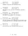
- FIGS. 4A and 4B show an update example of a tag when a cache miss occurs in the previously-proposed technology.
- Each of the four WAYs (3a-0, 3a-1, 3a-2, and 3a-3) forming the cache tag 3a in the CPU 2a stores an address (0, 1, 2, and 3) (the cache tag 3a in the CPU 2a is in the full state).
- a read request is issued in the CPU 2a after a cache miss.
- a read request for an address 5 is issued (step 101.
- a “step” is referred to as "S").
- the CPU 2a determines, for example, the WAY[3a-0] of the cache tag 3a to be replaced, and deletes the address information (address 0) stored in the WAY [3a-0] (S102).
- the CPU 2a issues to the system controller 1 a read request for the address information (address 5) generated in S101 (S103).
- the system controller 1 determines, for example, the WAY [5a-2] to be replaced, and deletes the address information (address 2) stored in the WAY [5a-2].
- the address stored in the WAY [5a-2] to be replaced is also a target to be replaced in the cache tag 3a in the CPU 2a. Therefore, the system controller 1 requests (eviction request) the CPU 2a to delete the address (address 2) to be replaced (S104).
- the CPU 2a Upon receipt of the eviction request, the CPU 2a analyzes the command, and deletes the address information (address 2) about the WAY [3a-2] of the cache tag 3a (S105).
- the system controller 1 updates the WAY [5a-2] of the snoop tag 5a (the address 5 is stored in the WAY [5a-2]). Then, the system controller 1 transmits the data corresponding to the address information to the CPU 2a (S106).
- the CPU 2a receives the data from the system controller 1, writes the data to the cache data 4a, and updates the WAY [3a-0] of the cache tag 3a by the address corresponding to the data (S107).
- a read request is issued after a cache miss in the CPU 2a again. For example, a read request for an address 6 is issued (S108). At this time, since there is available space in the cache tag 3 (WAY 3a-2]), the deleting process described in S102 is not performed, but the CPU 2a issues a read request for the address 6 to the system controller 1 (S109).
- the system controller 1 deletes the address information (address 1) stored in the WAY [5a-1] when, for example, the WAY [5a-1] is determined as a replacement target.
- the address stored in the WAY [5a-1] to be replaced is also a replacement target in the cache tag 3a. Therefore, the system controller 1 requests the CPU 2a to delete the address (address 1) to be replaced (eviction request) (S110).
- the CPU 2a Upon receipt of the eviction request, the CPU 2a analyzes the command, and deletes the address information (address 1) stored in the WAY [3a-1] of the cache tag 3a (S111).
- the system controller 1 updates the WAY [5a-1] of the snoop tag 5a (the address 6 is stored in the WAY [5a-1]). Then, the system controller 1 transmits the data corresponding to the address to the CPU 2a (S112).
- the CPU 2a receives the data from the system controller 1, writes it to the cache data 4a, and updates the WAY [3a-0] of the cache tag 3a by the address corresponding to the data (S113).
- the replacement target of the CPU 2 does not always match that of the system controller 1. Accordingly, the CPU 2 allows excess replacement. As a result, there can be a plurality of available WAYs, thereby possibly raising a cache miss rate.
- the documents relating to the related art in this technical field can be the Japanese Published Patent Application No. H5-204869 , the Japanese Published Patent Application No. H7-311711 , the Japanese Published Patent Application No. H10-214222 , and the Japanese Published Patent Application No. H5-265970 .
- An information processing system embodying the present invention includes:
- a method of updating a cache tag and a snoop tag of an information processing system having one or more processors including cache memory of a plurality of ways formed by a cache tag and a cache data area and executing an instruction and processing data, and a processor control device for transmitting information to the processors at a request from the processors, and having the number of ways of the snoop tag as tag information corresponding to the cache tag of each processor larger than the number of ways of the cache tag of the processors, wherein the processor control device transmits the data corresponding to the address information to the processors by updating available ways according to the address information as a target of a read request if the processors issue the read request when a cache miss occurs and there are the available ways of the snoop tag.
- An information processing board embodying the present invention includes:
- An information processing system embodying the present invention includes: one or more processors having cache memory including a cache tag having a plurality of ways and a cache data area, executing an externally received instruction, and processing data; and a processor control device transmitting a reply to the processors at a read request from the processors, having a snoop tag as tag information corresponding to the cache tag of the processor, and having the number of ways of the snoop tag larger than the number of ways of the cache tag of the processor.
- the cache miss rate can be reduced.
- the information processing system transmits data corresponding to address information to the processors by the processor control device updating available ways according to the address information as a target of a read request if the processors issue the read request when a cache miss occurs and there are available ways of the snoop tag.
- the replacement of a snoop tag can be reduced, thereby decreasing the cache miss rate.
- the processor control device deletes any of the address information stored in the way of the snoop tag, and notifies the processor of the information that the address information is deleted.
- the information that the address information stored in any way of the cache tag is expelled is not transmitted from the processor to the processor control device.
- An embodiment of the present invention provides an information processing system having the number of WAYs stored in the snoop tag in the system controller larger than the number of WAYs in the CPU cache. Thus, excess replacement of the tags in the CPU can be suppressed.
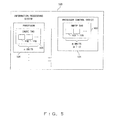
- FIG. 5 shows the concept of the configuration of the information processing system according to a mode for embodying the present invention.
- the mode for embodying the present invention is an information processing system having a chip set loaded with a CPU having cache, and a system controller having a copy of the tag of the cache (hereinafter referred to as a snoop tag), and is based on the information processing system having the CPU that issues no replacement information about a cache tag.
- An information processing system 100 is provided with one or more processors 104 and a processor control device 101.
- the processor 104 has cache memory which includes a cache tag 105 including a plurality of ways 106 and cache data, executes externally received information, and processes data.
- the processor control device 101 transmits a reply to the processor 104 on the basis of a read request from the processor 104.
- the processor control device 101 has a snoop tag 102 as tag information corresponding to the cache tag 105 of each processor 104.
- the number of ways 103 (m: any integer) of the snoop tag 102 is larger than the number of the ways 106 (n: any integer) of the cache tag 105 (m > n).
- the processor control device 101 If there is a read request from the processor 104 when a cache miss occurs, the processor control device 101, and if there is available way 103 of the snoop tag 102, then it updates the available way according to the address information about the data as a target of the read request, and can transmit data corresponding to the address information to the processor 104.
- the cache miss rate can be decreased.
- unnecessary deletion of the WAY of the cache tag on the CPU side can be suppressed.
- the processor control device 101 deletes any of the address information stored in the way 103 of the snoop tag 102, and notifies the processor 104 of the information (eviction request) that the address information is to be deleted.
- a snoop tag stores the same contents as the cache tag. Howerer, since the number of WAYs of the snoop tag is larger than the number of the WAYs of the cache tag, an address not stored in the cache is stored. Therefore, there is the possibility that when the snoop tag is full, the optionally selected WAY is the address not stored on the cache side. Accordingly, when an eviction request is issued from the system controller, there is a lower possibility that the address specified by the eviction request is stored on the cache side, and there is a lower possibility that the process of deleting the address of the WAY of the cache tag is performed. As a result, there is a lower possibility that there is an available WAY of a cache tag, thereby decreasing the cache miss rate.
- FIG. 6 shows the configuration of the tag of the information processing system according to a mode for embodying the present invention.
- the number of WAYs of the snoop tags 5a and 5b in the system controller 1 is larger by one than the number of WAYs of the cache tags 3a and 3b in the CPUs 2a and 2b. That is, in the present mode for embodying the present invention, the number of WAYs of the cache tags 3a and 3b in the CPUs 2a and 2b is 4 while the number of WAYs of the snoop tags 5a and 5b in the system controller 1 is 5.
- 6a-Aa, 6a-Ab indicates a cache read request from the CPUs 2a and 2b.
- 6a-Ba, 6a-Bb indicates an eviction request from the system controller 1.
- 6c-Ca, 6a-Cb indicates the cache data transmitted from the CPUs 2a and 2b.
- FIGS. 7A-7C show the packet formats of a cache read request, an eviction request, and cache data.
- FIG. 7A shows the packet format of the cache read request 6a-Aa, 6a-Ab from the CPU.
- the cache read request is configured by an [ID] field, an [OPC] field, and an [address] field.
- the [ID] field stores the information identifying from which CPU the read request has been issued.
- the [OPC] field stores a read instruction.
- the [address] field stores the address of the main memory storing the data as a target of the read request.
- FIG. 7B shows the packet format of the eviction request 6a-Ba, 6a-Bb from the system controller.
- the eviction request is configured by an [OPC] field and an [address] field.
- the [OPC] field stores an eviction instruction.
- the [address] field stores the same address as the WAY of the snoop tag to be replaced.
- FIG. 7C shows the packet format of the cache data 6c-Ca, 6a-Cb transmitted from the system controller to the CPU.
- the cache data is configured by an [ID] field and a [data] field.
- the [data] field stores data.
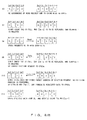
- FIGS. 8A and 8B show examples of updating the tag when a cache miss occurs according to the present mode for embodying the present invention. Described below are mainly the cache tag 3a and the snoop tag 5a corresponding to the cache tag 3a for convenience in explanation.
- the cache tag 3a in the CPU 2a is configured by 4 WAYs.
- Each WAY (3a-0, 3a-1, 3a-2, and 3a-3) stores an address (0,1,2, and 3) (the cache tag 3a in the CPU 2 is in the full state).
- the snoop tag 5a is configured by 5 WAYs, 4 WAYs (5a-0, 5a-1, 5a-2, and 5a-3) of which respectively store addresses (0. 1, 2, and 3).
- the WAY [5a-4] of the snoop tag 5a is available.
- a read request is issued when a cache miss occurs. For example, a read request for the data corresponding to the address 5 is issued (S1).
- the CPU 2a determines, for example, the WAY [3a-0] of the cache tag 3a as a replacement target, and deletes the address information (address 0) stored in the WAY [3a-0] (S2).
- the CPU 2a issues to the system controller 1 a read request for the address information (address 5) generated in S1 (S3).
- the system according to the present mode for embodying the present invention is a system not issuing a replace request from the CPU 2a.
- the system controller if the snoop tag 5a is full, it is necessary for the system controller to delete the address information about any WAY in the snoop tag.
- the WAY [5a-4] of the snoop tag 5a is available in the status in S3, it is not necessary to perform the process of deleting the information about the WAY of the snoop tag 5a. Accordingly, an eviction request to the CPU 2a relating to the deleting process is not issued.
- the system controller 1 updates the WAY [5a-4] of the snoop tag 5a, and the address 5 is stored in the WAY [5a-4]. Furthermore, the system controller 1 transmits the target data of the read request corresponding to the address to the CPU 2a (S4).
- the CPU 2a receives the data from the system controller 1, writes the data to the cache data 4a, and updates the WAY [3a-0] of the cache tag 3a according to the address (address 5) corresponding to the data (S5).
- the CPU 2a issues a read request after a cache miss. For example, a read request for the address 6 is issued (S6) .
- the CPU 2a determines the WAY [3a-1] of the cache tag 3a as a replacement target, and deletes the address information (address 1) stored in the WAY [3a-1] (S7).
- the CPU 2a issues to the system controller 1 a read request for data corresponding to the address 6 (S8).
- the system controller 1 determines, for example, the WAY [5a-1] as a replacement target, and deletes the address information (address 1) stored in the WAY [5a-1].
- the address information stored in the WAY (5a-1] as a replacement target is also to be replaced in the cache tag 3a. Therefore, the system controller 1 issues to the CPU 2a a request to delete the address (address 1) to be replaced (eviction request) (S9).
- the CPU 2a receives the eviction request. However, since the CPU 2a does not hold the target address of the eviction request, no eviction process is performed. Then, the system controller 1 updates the WAY [5a-1] of the snoop tag 5a, and the address 6 is stored in the WAY [5a-1] of the snoop tag 5a. Furthermore, the system controller 1 transmits the target data of the read request corresponding to the address to the CPU 2a (S10).
- the CPU 2a receives the data from the system controller 1, writes the data to the cache data 4a, updates the WAY [3a-0] of the cache tag 3a according to the address corresponding to the data, and the address 6 is stored in the WAY [3a-2] of the cache tag 3a (S11).
- FIG. 9 is a flowchart of updating a tag when a cache miss occurs according to the present mode for embodying the present invention.
- CPU 2 a read request due to a cache miss is issued (S21). Then, the CPU 2 determine whether or not the cache tag 3 is full (S22).
- a WAY can be deleted in, for example, the LRU (least recently used) system and other well-known systems.
- the CPU 2 issues a read request to the system controller 1 (S24).
- the system controller 1 determines whether or not the snoop tag 5 corresponding to the CPU 2 which has issued the read request is full (S25).
- the system controller 1 updates the available WAY, and the address as a target of the read request is stored in the available MAY (S29) .
- the system controller 1 selects a WAY in the snoop tag 5 at random, and deletes the address stored in the selected WAY. Furthermore, the system controller 1 issues an eviction request to the CPU 2 that has issued the read request (S26).
- the CPU 2 determines whether or not the address as a target of the eviction request is stored in the cache tag 3 (S27).
- control is passed to S30.
- the CPU 2 deletes the address of the WAY of the cache tag 3 storing the address as a target of the eviction request (S28) Then, the system controller 1 updates the WAY of the snoop tag 5 deleted in S26 (S29).
- the system controller 1 transmits the data specified in the read request to the CPU 2 that has issued the read request (S30), and updates the WAY of the cache tag 3 according to the address corresponding to the transmitted data (S31).
- the number of WAYs of the snoop tag 5 in the system controller 1 is one larger than the number of WAYs of the cache tag 3 in the CPU 2, but the relationship between the numbers of WAYs is not limited to this application. That is, it is accepted if the number of WAYs of the snoop tag 5 is larger than the number of WAYs of the cache tag 3.
- the snoop tag can store those addresses not stored in the cache because the number of WAYs of the snoop tag 5 is larger than the number of WAYs of the cache tag 3. Therefore, if the snoop tag is full, there is the possibility that an optionally selected WAY can be an address not stored on the cache side. Therefore, when an eviction request is issued from the system controller, there is a lower possibility that the address specified in the eviction request is stored on the cache side. As a result, there is a lower possibility that the process of deleting an address of a WAY of a cache tag is deleted. Accordingly, there is a lower possibility that there is an available WAY of a cache tag, thereby reducing the cache miss rate.
- the present invention is not limited to the above-mentioned mode for embodying the present invention, but can be realized with various configurations or aspects within the scope of the gist of the present invention.
- the replacement of the snoop tag 5 in the system controller 1 can be reduced.
- excess replacement performed when the cache tag 3 in the CPU 2 is full can be reduced.
- a cache miss rate can be decreased.
Landscapes
- Engineering & Computer Science (AREA)
- Theoretical Computer Science (AREA)
- Physics & Mathematics (AREA)
- General Engineering & Computer Science (AREA)
- General Physics & Mathematics (AREA)
- Software Systems (AREA)
- Memory System Of A Hierarchy Structure (AREA)
Abstract
Description
- The present invention relates to a tag configuration of a system in which a processor bus has a plurality of CPU cores and a system controller has a snoop tag as a copy of cache in a CPU.
- Generally, cache memory is used as means for improving the throughput in accessing main storage slower than a CPU. The cache memory is normally located between the CPU and the main storage, and is normally provided in the CPU.
- When the cache memory is compared with a storage device (external memory) used in the main storage, the cache memory is higher in access speed, but has a smaller capacity. Therefore, the data stored in the cache memory is a part of all data held in the external memory.
- If the cache memory stores data to be read, the data can be read at a high speed. However, unless there is data to be read in the cache memory, the data to be read is read by accessing the main storage, and the data is read at a lower speed.
- The cache memory is configured by cache (data area, or cache data) storing a part of data stored in the main storage and tag memory (tag area, or cache tag) staring a part (tag) of the address of the data stored in the cache.
- The processor is informed whether or not data required for execution is stored in the cache by comparing the address of the data with the tag in the tag memory. Unless necessary data is stored in the cache, the data is loaded into the cache from the main memory, and a part of the address of the data is loaded as a new tag into the tag memory. To load the new tag into the tag memory, it is necessary to expel the tag which is not required or is considered unnecessary.
- The tag memory is formed by a plurality of ways (WAYs). To determine the tags to be expelled (to update the tags) before loading a new tag, the tag is assigned LRU (least recently used) information in advance.
- For example, when a tag is written, an LRU information generation circuit generates the LRU information indicating the tag to be next replaced, and the information is written corresponding to the tag to the tag memory. Therefore, a line as a unit of a read/write to the tag memory stores a tag and its LRU information. When a new tag is loaded into the tag memory, a supplemented WAY information generation circuit determines which tag is to be supplemented to which way using the LRU information added to each tag.
- A match determination circuit compares (a part of) the address of the data required by the processor with a predetermined tag stored in the tag memory, and determines whether or not the data is stored in the cache.
- After the determination, (the line of) the tag read from the tag memory is written again to the tag memory. That is, the tag rewriting cycle is executed after the determination because it cannot be stated that the LRU information is correct LRU information reflecting the result of the determination unless the LRU information about the line of the tag is rewritten to the tag memory. Then, based on the result of the hit/mishit of the line, the LRU information generation circuit generates new LRU information and stores it in the tag memory. Thus, the LRU control of writing a new tag using the LRU information is performed.
- FIG. 1 shows the entire information processing system (chip set) provided with a common multiprocessor configuration. In FIG. 3, the information processing system mainly includes a
system board 10, an input/output control unit 15, adata cross bar 17, and anaddress cross bar 16. Thesystem board 10 includes asystem controller 1, afirmware hub 11, aCPU 2, amemory controller 12,memory 13, aCPU bus 6, and afirmware hub bus 7. - The
CPU bus 6 connects thesystem controller 1 to theCPU 2. Thefirmware hub bus 7 connects thesystem controller 1 to thefirmware hub bus 7. Thedata cross bar 17 is a bus for transmitting data to or receiving data from thesystem board 10. Theaddress cross bar 16 is a bus for transmitting an address to or receiving an address from thesystem board 10. - The
system controller 1 is a device for controlling transmission/reception of data between theCPU 2 and thememory 13. Thefirmware hub 11 stores firmware. Thememory controller 12 controls the operation of thememory 13. - FIG. 2 shows the tag in the information processing system. In FIG. 2, the
system controller 1 is connected to theCPUs CPU buses CPU 2 is configured by a cache tag 3 (3a, 3b, 3c, and 3d) and cache data 4 (4a, 4b, 4c, and 4d). - The
system controller 1 is provided with a snoop tag 5 (5a, 5b, 5c, and 5d) corresponding to each cache tag 3 (3a, 3b, 3c, and 3d). - The
system controller 1 confirms whether or not the data as a target of a read request is held by other snooptags snoop tags CPU 2a issues the read request when a cache miss occurs. When the data as a target of the read request is held by other snooptags snoop tags system controller 1 acquires replacement information corresponding to the replace request from thesnoop tag 5 holding the tag and passes it to theCPU 2a. However, if nosnoop tag 5 holds the data as a target of the read request, thesystem controller 1 acquires the replacement information corresponding to the read request from the main storage, and passes it to theCPU 2a. - FIG. 3 shows an example of the configuration of a conventional tag. Mainly the CPU2a shown in FIG. 3 is explained below. The
cache tag 3a in theCPU 2a is formed by, for example, four WAYs (3a-0, 3a-1, 3a-2, and 3a-3). - On the other hand, the
snoop tag 5a of thesystem controller 1 corresponding to thecache tag 3a is also formed by four WAYs (5a-0, 5a-1, 5a-2, and 5a-3). Thus, in the conventional configuration, thecache tag 3 of theCPU 2 has the same number of WAYs as thesnoop tag 5 of thesystem controller 1. In this case, the following event can occur. - First, if the
cache tag 3 is full (that is, all WAYs forming the cache tag are in the write state) when a read request is issued (6a-Aa) after a cache miss from theCPU 2 to thesystem controller 1, then theCPU 2 expels the address from any of the WAY formingcache tag 3, and replaces it with the address of data as a target of a read request (replacement information). - In the above-mentioned system, there is no means for notifying the
system controller 1 from theCPU 2 of the replacement information about the address of which WAY is expelled, or the replacement information is not always notified even granting that there is the means. - Therefore, in the system having no means of notifying the
system controller 1 from theCPU 2 of the replacement information or having the system provided with a protocol in which delete information is not always given without fail although there is such means, thesystem controller 1 uniquely determines a snoop tag to be replaced. - FIGS. 4A and 4B show an update example of a tag when a cache miss occurs in the previously-proposed technology. Each of the four WAYs (3a-0, 3a-1, 3a-2, and 3a-3) forming the
cache tag 3a in theCPU 2a stores an address (0, 1, 2, and 3) (thecache tag 3a in theCPU 2a is in the full state). - First, a read request is issued in the
CPU 2a after a cache miss. For example, a read request for anaddress 5 is issued (step 101. Hereinafter, a "step" is referred to as "S"). - Then, the
CPU 2a determines, for example, the WAY[3a-0] of thecache tag 3a to be replaced, and deletes the address information (address 0) stored in the WAY [3a-0] (S102). - The
CPU 2a issues to the system controller 1 a read request for the address information (address 5) generated in S101 (S103). - In this example, since addresses are written to all WAYs of the
snoop tag 5a (full state), it is necessary to delete any WAY as a target to be replaced. - However, in the system receiving no replace request from the
CPU 2a, it is necessary for thesystem controller 1 to forcibly determine the address of which WAY of the snoop tag is to be replaced. - Then, the
system controller 1 determines, for example, the WAY [5a-2] to be replaced, and deletes the address information (address 2) stored in the WAY [5a-2]. - The address stored in the WAY [5a-2] to be replaced is also a target to be replaced in the
cache tag 3a in theCPU 2a. Therefore, thesystem controller 1 requests (eviction request) theCPU 2a to delete the address (address 2) to be replaced (S104). - Upon receipt of the eviction request, the
CPU 2a analyzes the command, and deletes the address information (address 2) about the WAY [3a-2] of thecache tag 3a (S105). - The
system controller 1 updates the WAY [5a-2] of thesnoop tag 5a (theaddress 5 is stored in the WAY [5a-2]). Then, thesystem controller 1 transmits the data corresponding to the address information to theCPU 2a (S106). - The
CPU 2a receives the data from thesystem controller 1, writes the data to thecache data 4a, and updates the WAY [3a-0] of thecache tag 3a by the address corresponding to the data (S107). - A read request is issued after a cache miss in the
CPU 2a again. For example, a read request for anaddress 6 is issued (S108). At this time, since there is available space in the cache tag 3 (WAY 3a-2]), the deleting process described in S102 is not performed, but theCPU 2a issues a read request for theaddress 6 to the system controller 1 (S109). - Then, since the snoop
tag 5a is full, thesystem controller 1 deletes the address information (address 1) stored in the WAY [5a-1] when, for example, the WAY [5a-1] is determined as a replacement target. - The address stored in the WAY [5a-1] to be replaced is also a replacement target in the
cache tag 3a. Therefore, thesystem controller 1 requests theCPU 2a to delete the address (address 1) to be replaced (eviction request) (S110). - Upon receipt of the eviction request, the
CPU 2a analyzes the command, and deletes the address information (address 1) stored in the WAY [3a-1] of thecache tag 3a (S111). - The
system controller 1 updates the WAY [5a-1] of the snooptag 5a (theaddress 6 is stored in the WAY [5a-1]). Then, thesystem controller 1 transmits the data corresponding to the address to theCPU 2a (S112). - The
CPU 2a receives the data from thesystem controller 1, writes it to thecache data 4a, and updates the WAY [3a-0] of thecache tag 3a by the address corresponding to the data (S113). - Thus, with the previously-proposed configuration, the replacement target of the
CPU 2 does not always match that of thesystem controller 1. Accordingly, theCPU 2 allows excess replacement. As a result, there can be a plurality of available WAYs, thereby possibly raising a cache miss rate. - Meanwhile, the documents relating to the related art in this technical field can be the
Japanese Published Patent Application No. H5-204869 Japanese Published Patent Application No. H7-311711 Japanese Published Patent Application No. H10-214222 Japanese Published Patent Application No. H5-265970 - Accordingly, it is desirable to reduce the cache miss rate and suppress the degradation of the performance by preventing excess replacement of a cache tag in the CPU in the information processing system in which the information stored in which WAY is expelled is not notified from the CPU to the system controller.
- An information processing system embodying the present invention includes:
- one or more processors having cache memory including a cache tag having a plurality of ways and a cache data area, executing an externally received instruction, and processing data; and
- a processor control device transmitting a reply to the processors at a read request from the processors, having a snoop tag as tag information corresponding to the cache tag of the processor, and having the number of ways of the snoop tag larger than the number of ways of the cache tag of the processor.
- According to an embodiment of the present invention there is provided a method of updating a cache tag and a snoop tag of an information processing system having one or more processors including cache memory of a plurality of ways formed by a cache tag and a cache data area and executing an instruction and processing data, and a processor control device for transmitting information to the processors at a request from the processors, and having the number of ways of the snoop tag as tag information corresponding to the cache tag of each processor larger than the number of ways of the cache tag of the processors, wherein the processor control device transmits the data corresponding to the address information to the processors by updating available ways according to the address information as a target of a read request if the processors issue the read request when a cache miss occurs and there are the available ways of the snoop tag.
- An information processing board embodying the present invention includes:
- one or more processors having cache memory including a cache tag having a plurality of ways and a cache data area, executing an externally received instruction, and processing data; and
- a processor control device transmitting a reply to the processors at a read request from the processors, having a snoop tag as tag information corresponding to the cache tag of the processor, and having the number of ways of the snoop tag larger than the number of ways of the cache tag of the processor.
-
- FIG. 1 shows the entire information processing system (chip set) having a common multiprocessor configuration;
- FIG. 2 shows a tag in the information processing system;
- FIG. 3 shows an example of the previously-proposed configuration of the tag;
- FIG. 4A shows an example (1) of updating a tag when a cache miss occurs in the previously-proposed technology;
- FIG. 4B shows an example (2) of updating a tag when a cache miss occurs in the previously-proposed technology;
- FIG. 5 shows the concept of the configuration of the information processing system according to a mode for embodying the present invention;
- FIG. 6 shows the configuration of the tag in the information processing system according to a mode for embodying the present invention;
- FIG. 7A shows the format of a packet of a cache read request;
- FIG. 7B shows the format of a packet of a eviction request;
- FIG. 7C shows the format of a packet of a cache data;
- FIG. 8A shows an example (1) of updating a tag when a cache miss occurs according to a mode for embodying the present invention;
- FIG. 8B shows an example (2) of updating a tag when a cache miss occurs according to a mode for embodying the present invention; and
- FIG. 9 is a flowchart of updating a tag when a cache miss occurs according to a mode for embodying the present invention.
- An information processing system embodying the present invention includes: one or more processors having cache memory including a cache tag having a plurality of ways and a cache data area, executing an externally received instruction, and processing data; and a processor control device transmitting a reply to the processors at a read request from the processors, having a snoop tag as tag information corresponding to the cache tag of the processor, and having the number of ways of the snoop tag larger than the number of ways of the cache tag of the processor.
- With the above-mentioned configuration, the cache miss rate can be reduced.
- The information processing system transmits data corresponding to address information to the processors by the processor control device updating available ways according to the address information as a target of a read request if the processors issue the read request when a cache miss occurs and there are available ways of the snoop tag.
- With the above-mentioned configuration, the replacement of a snoop tag can be reduced, thereby decreasing the cache miss rate.
- In the information processing system, during the update of available ways, no request to delete arbitrarily address information from a way storing the arbitrarily address information is not issued from the processor control device to the processor.
- With the above-mentioned configuration, no eviction request is transmitted to the CPU. Therefore, unnecessary deletion of WAYs of a cache tag on the CPU side can be suppressed.
- In the information processing system, when the processor issues a read request when a cache miss occurs, and if there is no available way of the snoop tag, the processor control device deletes any of the address information stored in the way of the snoop tag, and notifies the processor of the information that the address information is deleted.
- With the configuration, since the number of WAYs of the snoop tag is larger than the number of WAYs of the cache tag. Therefore, as the snoop tag is updated, the stored contents of the snoop tag and the cache tag are conspicuously different, and the possibility that the same addresses exist in the both tags as compared with the conventional technology.
- In the information processing system, the information that the address information stored in any way of the cache tag is expelled is not transmitted from the processor to the processor control device.
- With the configuration, an event that an excess available WAY occurs in this system can be suppressed.
- An embodiment of the present invention provides an information processing system having the number of WAYs stored in the snoop tag in the system controller larger than the number of WAYs in the CPU cache. Thus, excess replacement of the tags in the CPU can be suppressed.
- Described below are the details of the mode for embodying the present invention.
- FIG. 5 shows the concept of the configuration of the information processing system according to a mode for embodying the present invention. The mode for embodying the present invention is an information processing system having a chip set loaded with a CPU having cache, and a system controller having a copy of the tag of the cache (hereinafter referred to as a snoop tag), and is based on the information processing system having the CPU that issues no replacement information about a cache tag.
- An
information processing system 100 according to a mode for embodying the present invention is provided with one ormore processors 104 and aprocessor control device 101. - The
processor 104 has cache memory which includes acache tag 105 including a plurality ofways 106 and cache data, executes externally received information, and processes data. - The
processor control device 101 transmits a reply to theprocessor 104 on the basis of a read request from theprocessor 104. Theprocessor control device 101 has a snooptag 102 as tag information corresponding to thecache tag 105 of eachprocessor 104. The number of ways 103 (m: any integer) of the snooptag 102 is larger than the number of the ways 106 (n: any integer) of the cache tag 105 (m > n). - If there is a read request from the
processor 104 when a cache miss occurs, theprocessor control device 101, and if there isavailable way 103 of the snooptag 102, then it updates the available way according to the address information about the data as a target of the read request, and can transmit data corresponding to the address information to theprocessor 104. - When the available way is updated, a request to delete the address information from the way storing predetermined address information in the
ways 106 of thecache tag 105 is not issued from theprocessor control device 101 to theprocessor 104. - Thus, since the replacement of the snoop
tag 102 can be reduced, the cache miss rate can be decreased. In addition, since an eviction request is not reported to the CPU, unnecessary deletion of the WAY of the cache tag on the CPU side can be suppressed. - If there is a read request from the
processor 104 when a cache miss occurs, and there is noavailable way 103 of the snooptag 102, then theprocessor control device 101 deletes any of the address information stored in theway 103 of the snooptag 102, and notifies theprocessor 104 of the information (eviction request) that the address information is to be deleted. - In an embodiment of the present invention, a snoop tag stores the same contents as the cache tag. Howerer, since the number of WAYs of the snoop tag is larger than the number of the WAYs of the cache tag, an address not stored in the cache is stored. Therefore, there is the possibility that when the snoop tag is full, the optionally selected WAY is the address not stored on the cache side. Accordingly, when an eviction request is issued from the system controller, there is a lower possibility that the address specified by the eviction request is stored on the cache side, and there is a lower possibility that the process of deleting the address of the WAY of the cache tag is performed. As a result, there is a lower possibility that there is an available WAY of a cache tag, thereby decreasing the cache miss rate.
- Described below is a mode for embodying the present invention.
- FIG. 6 shows the configuration of the tag of the information processing system according to a mode for embodying the present invention. As compared with FIG. 3, the number of WAYs of the snoop tags 5a and 5b in the
system controller 1 is larger by one than the number of WAYs of the cache tags 3a and 3b in theCPUs CPUs system controller 1 is 5. - In FIG. 6, 6a-Aa, 6a-Ab indicates a cache read request from the
CPUs system controller 1. 6c-Ca, 6a-Cb indicates the cache data transmitted from theCPUs - FIGS. 7A-7C show the packet formats of a cache read request, an eviction request, and cache data. FIG. 7A shows the packet format of the cache read
request 6a-Aa, 6a-Ab from the CPU. The cache read request is configured by an [ID] field, an [OPC] field, and an [address] field. The [ID] field stores the information identifying from which CPU the read request has been issued. The [OPC] field stores a read instruction. The [address] field stores the address of the main memory storing the data as a target of the read request. - FIG. 7B shows the packet format of the
eviction request 6a-Ba, 6a-Bb from the system controller. The eviction request is configured by an [OPC] field and an [address] field. The [OPC] field stores an eviction instruction. The [address] field stores the same address as the WAY of the snoop tag to be replaced. - FIG. 7C shows the packet format of the
cache data 6c-Ca, 6a-Cb transmitted from the system controller to the CPU. The cache data is configured by an [ID] field and a [data] field. The [data] field stores data. - FIGS. 8A and 8B show examples of updating the tag when a cache miss occurs according to the present mode for embodying the present invention. Described below are mainly the
cache tag 3a and the snooptag 5a corresponding to thecache tag 3a for convenience in explanation. - First, the
cache tag 3a in theCPU 2a is configured by 4 WAYs. Each WAY (3a-0, 3a-1, 3a-2, and 3a-3) stores an address (0,1,2, and 3) (thecache tag 3a in theCPU 2 is in the full state). - On the other hand, the snoop
tag 5a is configured by 5 WAYs, 4 WAYs (5a-0, 5a-1, 5a-2, and 5a-3) of which respectively store addresses (0. 1, 2, and 3). The WAY [5a-4] of the snooptag 5a is available. - First, in the
CPU 2a, a read request is issued when a cache miss occurs. For example, a read request for the data corresponding to theaddress 5 is issued (S1). - Then, the
CPU 2a determines, for example, the WAY [3a-0] of thecache tag 3a as a replacement target, and deletes the address information (address 0) stored in the WAY [3a-0] (S2). - The
CPU 2a issues to the system controller 1 a read request for the address information (address 5) generated in S1 (S3). - Assume that the system according to the present mode for embodying the present invention is a system not issuing a replace request from the
CPU 2a. In this case, if the snooptag 5a is full, it is necessary for the system controller to delete the address information about any WAY in the snoop tag. However, since the WAY [5a-4] of the snooptag 5a is available in the status in S3, it is not necessary to perform the process of deleting the information about the WAY of the snooptag 5a. Accordingly, an eviction request to theCPU 2a relating to the deleting process is not issued. - In this case, the
system controller 1 updates the WAY [5a-4] of the snooptag 5a, and theaddress 5 is stored in the WAY [5a-4]. Furthermore, thesystem controller 1 transmits the target data of the read request corresponding to the address to theCPU 2a (S4). - The
CPU 2a receives the data from thesystem controller 1, writes the data to thecache data 4a, and updates the WAY [3a-0] of thecache tag 3a according to the address (address 5) corresponding to the data (S5). - Again, the
CPU 2a issues a read request after a cache miss. For example, a read request for theaddress 6 is issued (S6) . At this time, since thecache tag 3a is full, theCPU 2a , for example, determines the WAY [3a-1] of thecache tag 3a as a replacement target, and deletes the address information (address 1) stored in the WAY [3a-1] (S7). - Then, the
CPU 2a issues to the system controller 1 a read request for data corresponding to the address 6 (S8). - Since the snoop
tag 5a is full in the state in S8, thesystem controller 1 determines, for example, the WAY [5a-1] as a replacement target, and deletes the address information (address 1) stored in the WAY [5a-1]. - The address information stored in the WAY (5a-1] as a replacement target is also to be replaced in the
cache tag 3a. Therefore, thesystem controller 1 issues to theCPU 2a a request to delete the address (address 1) to be replaced (eviction request) (S9). - Then, the
CPU 2a receives the eviction request. However, since theCPU 2a does not hold the target address of the eviction request, no eviction process is performed. Then, thesystem controller 1 updates the WAY [5a-1] of the snooptag 5a, and theaddress 6 is stored in the WAY [5a-1] of the snooptag 5a. Furthermore, thesystem controller 1 transmits the target data of the read request corresponding to the address to theCPU 2a (S10). - The
CPU 2a receives the data from thesystem controller 1, writes the data to thecache data 4a, updates the WAY [3a-0] of thecache tag 3a according to the address corresponding to the data, and theaddress 6 is stored in the WAY [3a-2] of thecache tag 3a (S11). - Thus, if a cache miss occurs when the
cache tag 3a is full, then the replacement of thecache tag 3a is performed only immediately after a read request is issued due to a cache miss. That is, there is only one available WAY in thecache tag 3a when the tag is updated, and two or more available WAYs are not detected, thereby excess replacement is not performed. The explanation given by referring to FIGS. 8A and 8B is given in detail by referring to FIG. 9. - FIG. 9 is a flowchart of updating a tag when a cache miss occurs according to the present mode for embodying the present invention. First, in
CPU 2, a read request due to a cache miss is issued (S21). Then, theCPU 2 determine whether or not thecache tag 3 is full (S22). - Unless the
cache tag 3 is full, that is, if there is an available WAY in the cache tag 3 ("NO" in S22), then control is passed to S24. - If the
cache tag 3 is full, that is, if there is no available WAY in the cache tag 3 ("YES" in S22), and an optional WAY is deleted from the cache tag 3 (S23). At this time, a WAY can be deleted in, for example, the LRU (least recently used) system and other well-known systems. - Next, the
CPU 2 issues a read request to the system controller 1 (S24). Thesystem controller 1 determines whether or not the snooptag 5 corresponding to theCPU 2 which has issued the read request is full (S25). - Unless the snoop
tag 5 is full, that is, if there is an available WAY in the snoop tag 5 ("NO" in S25), thesystem controller 1 updates the available WAY, and the address as a target of the read request is stored in the available MAY (S29) . - When the snoop
tag 5 is full, that is, when there is no available WAY ("YES" in S25), thesystem controller 1 selects a WAY in the snooptag 5 at random, and deletes the address stored in the selected WAY. Furthermore, thesystem controller 1 issues an eviction request to theCPU 2 that has issued the read request (S26). - Thus, the
CPU 2 determines whether or not the address as a target of the eviction request is stored in the cache tag 3 (S27). - Unless the address as a target of the eviction request is stored in the cache tag 3 ("NO" in S27), control is passed to S30.
- If the address as a target of the eviction request is stored in the cache tag 3 ("YES" in S27), the
CPU 2 deletes the address of the WAY of thecache tag 3 storing the address as a target of the eviction request (S28) Then, thesystem controller 1 updates the WAY of the snooptag 5 deleted in S26 (S29). - Then, the
system controller 1 transmits the data specified in the read request to theCPU 2 that has issued the read request (S30), and updates the WAY of thecache tag 3 according to the address corresponding to the transmitted data (S31). - In the present mode for embodying the present invention, the number of WAYs of the snoop
tag 5 in thesystem controller 1 is one larger than the number of WAYs of thecache tag 3 in theCPU 2, but the relationship between the numbers of WAYs is not limited to this application. That is, it is accepted if the number of WAYs of the snooptag 5 is larger than the number of WAYs of thecache tag 3. - Furthermore, although the same contents are stored in the snoop tag and the cache tag, the snoop tag can store those addresses not stored in the cache because the number of WAYs of the snoop
tag 5 is larger than the number of WAYs of thecache tag 3. Therefore, if the snoop tag is full, there is the possibility that an optionally selected WAY can be an address not stored on the cache side. Therefore, when an eviction request is issued from the system controller, there is a lower possibility that the address specified in the eviction request is stored on the cache side. As a result, there is a lower possibility that the process of deleting an address of a WAY of a cache tag is deleted. Accordingly, there is a lower possibility that there is an available WAY of a cache tag, thereby reducing the cache miss rate. - The present invention is not limited to the above-mentioned mode for embodying the present invention, but can be realized with various configurations or aspects within the scope of the gist of the present invention.
- According to an embodiment of the present invention, the replacement of the snoop
tag 5 in thesystem controller 1 can be reduced. As a result, excess replacement performed when thecache tag 3 in theCPU 2 is full can be reduced. Thus, a cache miss rate can be decreased.
Claims (14)
- An information processing system, comprising:one or more processors (104, 2a, 2b) having cache memory including a cache tag (105, 3a, 3b) having a plurality of ways (106, 3a-0 - 3a-3, 3b-0 - 3b-3 and a cache data area, executing an externally received instruction, and processing data; anda processor control device (101, 1) transmitting a reply to the processors at a read request from the processors, having a snoop tag (102, 5a, 5b) as tag information corresponding to the cache tag of the processor, and having a number of ways (103, 5a-0 - 5a-4, 5b-0 - 5b-4 of the snoop tag larger than a number of ways (106, 3a-0 - 3a-3, 3b-0 - 3b-3 of the cache tag of the processor.
- The system according to claim 1, wherein
if a cache miss occurs in the processors (104, 2a, 2b), if there is a data read request from the processor to the processor control device (101, 1), and if there is an available way of the snoop tag, then the processor control device updates the available way according to address information as a target of the read request, and transmits the data corresponding to the address information to the processors. - The system according to claim 2, wherein
when the available way is updated, the processor control device (101, 1) does not issue to the processor (104, 2a, 2b) a request to delete arbitrarily address information from a way storing the arbitrarily address information in the ways of the cache tag. - The system according to claim 1, wherein
if there is no available way of the snoop tag when the processor (104, 2a, 2b) issues a read request when a cache miss occurs, then the processor control device (101, 1) deletes any of the address information stored in the way of the snoop tag, and notifies the processor of the information that the address information is to be deleted. - The system according to claim 1, wherein
the information processing system adopts a system of not transmitting information, from the processor (104, 2a, 2b) to the processor control device (101, 1), that address information stored in any way of the cache tag is expelled when a cache miss occurs. - A method of updating a cache tag and a snoop tag of an information processing system having one or more processors (104, 2a, 2b) including cache memory of a plurality of ways (106, 3a-0 - 3a-3, 3b-0 - 3b-3) formed by a cache tag (105, 3a, 3b) and a cache data area and executing an instruction and processing data, and a processor control device (101, 1) for transmitting information to the processors at a request from the processors, and having a number of ways (103, 5a-0 - 5a-4, 5b-0 - 5b-4) of the snoop tag (102, 5a, 5b) as tag information corresponding to the cache tag of each processor larger than a number of ways (106, 3a-0 - 3a-3, 3b-0 - 3b-3) of the cache tag of the processors, wherein
the processor control device transmits data corresponding to the address information to the processors by updating available ways according to the address information as a target of a read request if the processors issue the read request when a cache miss occurs and there are the available ways of the snoop tag. - The method according to claim 6, wherein
when the available way is updated, the processor control device (101, 1) does not issue to the processor (104, 2a, 2b) a request to delete arbitrarily address information from a way storing the arbitrarily address information in the ways of the cache tag. - The method according to claim 6, wherein
if there is no available way of the snoop tag when the processor (104, 2a, 2b) issues an information read request when a cache miss occurs, then the processor control device (101, 1) deletes any of the address information stored in the way of the snoop tag, and notifies the processor of the information that the address information is to be deleted. - The method according to claim 6, wherein
the information processing system adopts a system of not transmitting information to the processor control device (101, 1) that address information stored in any way of the cache tag is expelled when a cache miss occurs. - An information processing board, comprising:one or more processors (104, 2a, 2b) having cache memory including a cache tag (105, 3a, 3b) having a plurality of ways (106, 3a-0 -3a-3, 3b-0 - 3b-3) and a cache data area, executing an externally received instruction, and processing data; anda processor control device (101, 1) transmitting a reply to the processors at a read request from the processors, having a snoop tag as tag information corresponding to the cache tag of the processor, and having a number of ways (103, 5a-0 - 5a-4, 5b-0 - 5b-4) of the snoop tag (102, 5a, 5b) larger than a number of ways (106, 3a-0 - 3a-3, 3b-0 - 3b-3) of the cache tag of the processor.
- The board according to claim 10, wherein
when there is a read request from the processor (104, 2a, 2b) when a cache miss occurs, and if there is an available way of the snoop tag, then the processor control device (101, 1) updates the available way according to address information as a target of the read request, and transmits data corresponding to the address information to the processor. - The board according to claim 11, wherein
when the available way is updated, the processor control device (101, 1) does not issue to the processor (104, 2a, 2b) a request to delete arbitrarily address information from a way storing the arbitrarily address information in the ways of the cache tag - The board according to claim 10, wherein
if there is no available way of the snoop tag when the processor (104, 2a, 2b) issues a read request when a cache miss occurs, then the processor control device (101, 1) deletes any of the address information stored in the way of the snoop tag, and notifies the processor of the information that the address information is to be deleted. - The board according to claim 10, wherein
the information processing system adopts a system of not transmitting information, from the processor (104, 2a, 2b) to the processor control device (101, 1), that address information stored in any way of the cache tag is expelled when a cache miss occurs.
Applications Claiming Priority (1)
| Application Number | Priority Date | Filing Date | Title |
|---|---|---|---|
| JP2006222439A JP2008046902A (en) | 2006-08-17 | 2006-08-17 | Information processing system, information processing board, and cache tag and snoop tag update method |
Publications (3)
| Publication Number | Publication Date |
|---|---|
| EP1895419A2 true EP1895419A2 (en) | 2008-03-05 |
| EP1895419A3 EP1895419A3 (en) | 2008-03-26 |
| EP1895419B1 EP1895419B1 (en) | 2013-01-23 |
Family
ID=38691934
Family Applications (1)
| Application Number | Title | Priority Date | Filing Date |
|---|---|---|---|
| EP07106976A Ceased EP1895419B1 (en) | 2006-08-17 | 2007-04-26 | Information processing system, information processing board, and method of updating cache tag and snoop tag |
Country Status (5)
| Country | Link |
|---|---|
| US (1) | US7805576B2 (en) |
| EP (1) | EP1895419B1 (en) |
| JP (1) | JP2008046902A (en) |
| KR (1) | KR100900012B1 (en) |
| CN (1) | CN101127011B (en) |
Families Citing this family (2)
| Publication number | Priority date | Publication date | Assignee | Title |
|---|---|---|---|---|
| JP5011885B2 (en) * | 2006-08-18 | 2012-08-29 | 富士通株式会社 | Snoop tag control device |
| JP5790532B2 (en) * | 2012-02-13 | 2015-10-07 | セイコーエプソン株式会社 | Electronic device and memory control method |
Family Cites Families (15)
| Publication number | Priority date | Publication date | Assignee | Title |
|---|---|---|---|---|
| JPS5373927A (en) * | 1976-11-10 | 1978-06-30 | Fujitsu Ltd | Replacing system of intermediate buffer memory |
| JPH02188847A (en) * | 1989-01-18 | 1990-07-24 | Agency Of Ind Science & Technol | Data exchange system for hierarchical cache memory |
| JP2862424B2 (en) | 1992-01-30 | 1999-03-03 | 株式会社日立製作所 | Information processing device |
| JPH05216765A (en) * | 1992-02-06 | 1993-08-27 | Hitachi Ltd | Hierarchical buffer storage device |
| JPH05265970A (en) | 1992-03-19 | 1993-10-15 | Toshiba Corp | Multi-processor system |
| US5590310A (en) | 1993-01-14 | 1996-12-31 | Integrated Device Technology, Inc. | Method and structure for data integrity in a multiple level cache system |
| JPH0713864A (en) * | 1993-06-25 | 1995-01-17 | Mitsubishi Electric Corp | Data processing device |
| TW243509B (en) | 1994-01-31 | 1995-03-21 | Ibm | Data processor with memory cache and method of operation |
| US5860109A (en) | 1996-07-01 | 1999-01-12 | Sun Microsystems, Inc. | Methods and apparatus for a coherence transformer for connecting computer system coherence domains |
| JPH1173370A (en) * | 1997-08-29 | 1999-03-16 | Fujitsu Ltd | Information processing device |
| JP3525050B2 (en) * | 1998-04-23 | 2004-05-10 | 富士通株式会社 | Main memory controller |
| JP2002007371A (en) * | 2000-06-23 | 2002-01-11 | Hitachi Ltd | L1 cache false share mitigation control method |
| JP2002055880A (en) * | 2000-08-08 | 2002-02-20 | Hitachi Ltd | Cache configuration method and processor system |
| JP3989312B2 (en) | 2002-07-05 | 2007-10-10 | 富士通株式会社 | Cache memory device and memory allocation method |
| US7143246B2 (en) * | 2004-01-16 | 2006-11-28 | International Business Machines Corporation | Method for supporting improved burst transfers on a coherent bus |
-
2006
- 2006-08-17 JP JP2006222439A patent/JP2008046902A/en active Pending
-
2007
- 2007-04-26 EP EP07106976A patent/EP1895419B1/en not_active Ceased
- 2007-04-27 US US11/740,984 patent/US7805576B2/en not_active Expired - Fee Related
- 2007-05-10 KR KR1020070045444A patent/KR100900012B1/en not_active Expired - Fee Related
- 2007-05-17 CN CN200710103962XA patent/CN101127011B/en not_active Expired - Fee Related
Also Published As
| Publication number | Publication date |
|---|---|
| US20080046662A1 (en) | 2008-02-21 |
| CN101127011B (en) | 2010-06-02 |
| KR100900012B1 (en) | 2009-05-29 |
| CN101127011A (en) | 2008-02-20 |
| EP1895419A3 (en) | 2008-03-26 |
| EP1895419B1 (en) | 2013-01-23 |
| KR20080016429A (en) | 2008-02-21 |
| JP2008046902A (en) | 2008-02-28 |
| US7805576B2 (en) | 2010-09-28 |
Similar Documents
| Publication | Publication Date | Title |
|---|---|---|
| EP4158486B1 (en) | Computer memory expansion device and method of operation | |
| KR101639672B1 (en) | Unbounded transactional memory system and method for operating thereof | |
| US8095732B2 (en) | Apparatus, processor, cache memory and method of processing vector data | |
| JP4474570B2 (en) | Cache coherency control method | |
| US8176261B2 (en) | Information processing apparatus and data transfer method | |
| EP2105838B1 (en) | Cache control apparatus, information processing apparatus, and cache control method | |
| KR101472967B1 (en) | Cache memory and method capable of write-back operation, and system having the same | |
| US6345320B1 (en) | DMA address buffer and cache-memory control system | |
| US20070005906A1 (en) | Information processing apparatus and cache memory control method | |
| EP1895419B1 (en) | Information processing system, information processing board, and method of updating cache tag and snoop tag | |
| US10775870B2 (en) | System and method for maintaining cache coherency | |
| JP5040121B2 (en) | Information processing apparatus, cache control method, and program | |
| CN109308167B (en) | Apparatus and system for tracking write requests, and method of controller | |
| JP4335298B2 (en) | Snoop control method and information processing apparatus | |
| US20090013130A1 (en) | Multiprocessor system and operating method of multiprocessor system | |
| JP7764605B2 (en) | Cache, cache management method, and electronic device | |
| JP5011885B2 (en) | Snoop tag control device | |
| JP2006185044A (en) | Multiprocessor system | |
| JP2004171469A (en) | Cache memory system and cache memory control method | |
| WO2007110914A1 (en) | Multiprocessor system and multiprocessor system operating method | |
| JP2017117203A (en) | Information processing device, arithmetic processing device, and method for controlling information processing device |
Legal Events
| Date | Code | Title | Description |
|---|---|---|---|
| PUAI | Public reference made under article 153(3) epc to a published international application that has entered the european phase |
Free format text: ORIGINAL CODE: 0009012 |
|
| PUAL | Search report despatched |
Free format text: ORIGINAL CODE: 0009013 |
|
| AK | Designated contracting states |
Kind code of ref document: A2 Designated state(s): AT BE BG CH CY CZ DE DK EE ES FI FR GB GR HU IE IS IT LI LT LU LV MC MT NL PL PT RO SE SI SK TR |
|
| AX | Request for extension of the european patent |
Extension state: AL BA HR MK YU |
|
| AK | Designated contracting states |
Kind code of ref document: A3 Designated state(s): AT BE BG CH CY CZ DE DK EE ES FI FR GB GR HU IE IS IT LI LT LU LV MC MT NL PL PT RO SE SI SK TR |
|
| AX | Request for extension of the european patent |
Extension state: AL BA HR MK YU |
|
| 17P | Request for examination filed |
Effective date: 20080922 |
|
| AKX | Designation fees paid |
Designated state(s): DE FR GB |
|
| 17Q | First examination report despatched |
Effective date: 20090918 |
|
| GRAP | Despatch of communication of intention to grant a patent |
Free format text: ORIGINAL CODE: EPIDOSNIGR1 |
|
| GRAS | Grant fee paid |
Free format text: ORIGINAL CODE: EPIDOSNIGR3 |
|
| GRAA | (expected) grant |
Free format text: ORIGINAL CODE: 0009210 |
|
| AK | Designated contracting states |
Kind code of ref document: B1 Designated state(s): DE FR GB |
|
| REG | Reference to a national code |
Ref country code: GB Ref legal event code: FG4D |
|
| REG | Reference to a national code |
Ref country code: DE Ref legal event code: R096 Ref document number: 602007028182 Country of ref document: DE Effective date: 20130321 |
|
| PLBE | No opposition filed within time limit |
Free format text: ORIGINAL CODE: 0009261 |
|
| STAA | Information on the status of an ep patent application or granted ep patent |
Free format text: STATUS: NO OPPOSITION FILED WITHIN TIME LIMIT |
|
| 26N | No opposition filed |
Effective date: 20131024 |
|
| REG | Reference to a national code |
Ref country code: DE Ref legal event code: R097 Ref document number: 602007028182 Country of ref document: DE Effective date: 20131024 |
|
| REG | Reference to a national code |
Ref country code: FR Ref legal event code: PLFP Year of fee payment: 10 |
|
| REG | Reference to a national code |
Ref country code: FR Ref legal event code: PLFP Year of fee payment: 11 |
|
| PGFP | Annual fee paid to national office [announced via postgrant information from national office to epo] |
Ref country code: FR Payment date: 20170313 Year of fee payment: 11 |
|
| PGFP | Annual fee paid to national office [announced via postgrant information from national office to epo] |
Ref country code: DE Payment date: 20170420 Year of fee payment: 11 Ref country code: GB Payment date: 20170426 Year of fee payment: 11 |
|
| REG | Reference to a national code |
Ref country code: DE Ref legal event code: R119 Ref document number: 602007028182 Country of ref document: DE |
|
| GBPC | Gb: european patent ceased through non-payment of renewal fee |
Effective date: 20180426 |
|
| PG25 | Lapsed in a contracting state [announced via postgrant information from national office to epo] |
Ref country code: DE Free format text: LAPSE BECAUSE OF NON-PAYMENT OF DUE FEES Effective date: 20181101 |
|
| PG25 | Lapsed in a contracting state [announced via postgrant information from national office to epo] |
Ref country code: GB Free format text: LAPSE BECAUSE OF NON-PAYMENT OF DUE FEES Effective date: 20180426 |
|
| PG25 | Lapsed in a contracting state [announced via postgrant information from national office to epo] |
Ref country code: FR Free format text: LAPSE BECAUSE OF NON-PAYMENT OF DUE FEES Effective date: 20180430 |