EP1894028B1 - Procede d'identification des fautes des composants d'un circuit analogue de traitement de signaux pour un transducteur de mesure - Google Patents
Procede d'identification des fautes des composants d'un circuit analogue de traitement de signaux pour un transducteur de mesure Download PDFInfo
- Publication number
- EP1894028B1 EP1894028B1 EP06763573A EP06763573A EP1894028B1 EP 1894028 B1 EP1894028 B1 EP 1894028B1 EP 06763573 A EP06763573 A EP 06763573A EP 06763573 A EP06763573 A EP 06763573A EP 1894028 B1 EP1894028 B1 EP 1894028B1
- Authority
- EP
- European Patent Office
- Prior art keywords
- signal
- processing circuit
- signal processing
- test
- svs
- Prior art date
- Legal status (The legal status is an assumption and is not a legal conclusion. Google has not performed a legal analysis and makes no representation as to the accuracy of the status listed.)
- Not-in-force
Links
Images

Classifications
-
- G—PHYSICS
- G01—MEASURING; TESTING
- G01R—MEASURING ELECTRIC VARIABLES; MEASURING MAGNETIC VARIABLES
- G01R31/00—Arrangements for testing electric properties; Arrangements for locating electric faults; Arrangements for electrical testing characterised by what is being tested not provided for elsewhere
- G01R31/28—Testing of electronic circuits, e.g. by signal tracer
- G01R31/2832—Specific tests of electronic circuits not provided for elsewhere
- G01R31/2836—Fault-finding or characterising
- G01R31/2839—Fault-finding or characterising using signal generators, power supplies or circuit analysers
-
- G—PHYSICS
- G01—MEASURING; TESTING
- G01R—MEASURING ELECTRIC VARIABLES; MEASURING MAGNETIC VARIABLES
- G01R27/00—Arrangements for measuring resistance, reactance, impedance, or electric characteristics derived therefrom
- G01R27/28—Measuring attenuation, gain, phase shift or derived characteristics of electric four pole networks, i.e. two-port networks; Measuring transient response
-
- G—PHYSICS
- G01—MEASURING; TESTING
- G01R—MEASURING ELECTRIC VARIABLES; MEASURING MAGNETIC VARIABLES
- G01R31/00—Arrangements for testing electric properties; Arrangements for locating electric faults; Arrangements for electrical testing characterised by what is being tested not provided for elsewhere
- G01R31/28—Testing of electronic circuits, e.g. by signal tracer
- G01R31/282—Testing of electronic circuits specially adapted for particular applications not provided for elsewhere
- G01R31/2829—Testing of circuits in sensor or actuator systems
-
- G—PHYSICS
- G01—MEASURING; TESTING
- G01R—MEASURING ELECTRIC VARIABLES; MEASURING MAGNETIC VARIABLES
- G01R31/00—Arrangements for testing electric properties; Arrangements for locating electric faults; Arrangements for electrical testing characterised by what is being tested not provided for elsewhere
- G01R31/28—Testing of electronic circuits, e.g. by signal tracer
- G01R31/2801—Testing of printed circuits, backplanes, motherboards, hybrid circuits or carriers for multichip packages [MCP]
- G01R31/2818—Testing of printed circuits, backplanes, motherboards, hybrid circuits or carriers for multichip packages [MCP] using test structures on, or modifications of, the card under test, made for the purpose of testing, e.g. additional components or connectors
-
- G—PHYSICS
- G05—CONTROLLING; REGULATING
- G05B—CONTROL OR REGULATING SYSTEMS IN GENERAL; FUNCTIONAL ELEMENTS OF SUCH SYSTEMS; MONITORING OR TESTING ARRANGEMENTS FOR SUCH SYSTEMS OR ELEMENTS
- G05B2219/00—Program-control systems
- G05B2219/30—Nc systems
- G05B2219/33—Director till display
- G05B2219/33331—Test, diagnostic of field device for correct device, correct parameters
Definitions
- the invention relates to a method for detecting component errors of an analog signal processing circuit, in particular for a transmitter.
- sensors are often used to detect different quantities.
- the signals from the sensors are fed to transmitters, where they are suitably prepared and displayed or forwarded to a higher-level unit via a fieldbus.
- transmitters include pressure and temperature transmitters, pH redox potential transmitters, conductivity transmitters, etc. for the corresponding measured values pressure, temperature, pH or conductivity value.
- the task of a sensor is to convert the physical / chemical measurand into an electrical signal.
- a first processing of the analog electrical signal takes place.
- it is converted into a digital signal and fed to a microcontroller in which the actual signal processing takes place.
- the circuit required for analog signal conditioning usually consists of a printed circuit board with a large number of analog components.
- test z. B. to perform an ICT (in circuit test).
- ICT in circuit test
- an analog signature analysis can be carried out.
- impedance signature By applying defined alternating voltage signals and tapping the resulting signals at individual test points, an analog signature analysis (ASA) can be carried out.
- impedance signature With known impedance of the components or the component group can be concluded from the current-voltage characteristic, which is also referred to as impedance signature, faulty components.
- test points are often no longer available. Ie. such ladder cards are not suitable for ICT tests.
- test circuit for an ICT test can be connected to an external test device with one or more test circuits and a signal processor.
- a transmitter which has a sensor for converting a detected measured variable into a sensor signal, which is processed in a signal conditioning device to a measurement signal.
- the transmitter has a controllable test signal generator for generating a test signal, which is added to the sensor signal additive.
- the test signal is a voltage signal, which is why the test signal generator is connected in series with the sensor to the signal conditioning device.
- a computing device checks on the basis of contained in the measurement signal portions of the test signal, the functionality of the transmitter.
- the object of the invention is a method for detecting component defects specify an analog signal processing circuit, in particular for a transmitter, which does not have the disadvantages mentioned above genarmiten which is particularly simple and inexpensive to carry out
- the essential idea of the invention is that at a first test point of the signal processing circuit, a test signal is generated, which is tapped at the signal output of the signal processing circuit and is evaluated in the digital unit of the transmitter.
- Elaborate testing equipment can also be omitted.
- the evaluation takes place in the already existing digital unit.
- the simplicity of the method is also characterized in that the response signal is evaluated only at a few selected times.
- the aim of the method is not to locate faulty components on the Signalvonatetungsscnies exactly but it should allow a simple decision whether in principle Banmaschineconcentr vodiegen. The exact localization can then be done in a further step or it is omitted in mass production for economic reasons entirely. The faulty Signalveratbeitongsschattung is then simply disposed of as defective.
- the test signal is trapezoidal, since with the defined rising and falling edges of such a signal differentiating properties of the signal processing circuit to be examined can be easily checked.
- the constant signal range of the signal allows the checking of integrating or amplifying circuit parts.
- a specific example in which the method according to the invention can be easily applied is a low-pass filter.
- the method can also be carried out in measuring operation of the sensor.
- the proportions of the measurement signal are simply taken into account in the evaluation.
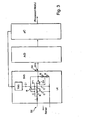
- FIG. 1 a block diagram of a typical transmitter MU for process automation technology is shown.
- a sensor S which is connected to a sensor module SM in the transmitter MU, detects z. As the temperature of a process medium.
- the analog sensor signal is processed with a subsequent digitization and evaluation in a microcontroller.
- the sensor module SM is connected to a processor module CPU.
- the processor module is essentially used for the calculation of the sensor signal with other process-relevant parameters, the preparation of the display for a display and the forwarding of the process values.
- the processor module CPU is connected to a display / operating unit AB, consisting of a display and a keyboard. Furthermore, the processor module CPU is connected to a communication module COM, which allows a connection of the transmitter MU to various communication systems. Examples of this are field buses such. As Profibus, Foundation Fieldbus, HART, etc. The corresponding signals are transmitted via a signal line SL. As a rule, transmitters are connected to a higher-level unit L.
- the higher-level unit L can be a controller (PLC) or a control system in a control room.
- the sensor module SM of the transmitter MU is shown as a block diagram.
- the sensor module SM consists essentially of a signal processing circuit SVS, an analog / digital converter AD and a microcontroller ⁇ C.
- the analog measurement signal of the sensor S is supplied to the signal processing circuit SVS.
- the signal processing circuit SVS is in Fig. 3 as part of the sensor module SM shown in more detail. It has as analog components a plurality of resistors R, a plurality of capacitors C, a coil L and an operational amplifier OA, which are arranged on a printed circuit board LK on. In addition, there is still a test signal generator TSG on the PCB LK.
- the signal processing circuit SVS is used for the analog preparation of the measurement signal MS.
- the signal processing circuit SVS is a filter circuit, the details of which should not be discussed. Transmitters use different signal processing circuits depending on the sensor type.
- the processed measurement signal is fed via a signal output SA from the signal processing circuit SVS to an analog / digital converter AD. After digitizing the conditioned measurement signal, the digitized measurement signal is further processed in a microcontroller .mu.C and then forwarded to the processor module CPU.
- a test signal TS can be capacitively coupled via a capacitor C1 to a test point TP1 of the signal processing circuit SVS.
- test signal TS associated with the response signal AS is supplied via the signal output SA, which serves as a second test point TP2, the A / D converter and then the microcontroller ⁇ C for evaluation.
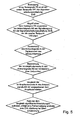
- test signal TS generated in the test signal generator TSG is coupled into the signal processing circuit SVS (method step a).
- test point TP1 is not directly connected to the signal input SE.
- the response signal AS associated with the test signal TS is detected at the signal output SA, the test point TP2 (method step b).
- the response signal AS is evaluated after its digitization in the microcontroller .mu.C as a digital unit (method step c).
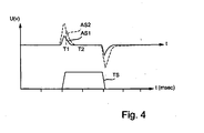
- the amplitudes of the response signal AS are determined at at least two specific times T1 and T2.
- the actual amplitude values AI1 and AI2 at the times T1 and T2 are compared with desired amplitude values AS and AS2 for the respective times T1 T2.
- the corresponding setpoints must be stored in the microcontroller .mu.C. If there is a significant deviation, an error message will be generated and / or an O.K message will be generated (step e).
- Fig. 4 are shown as a special test signal, a trapezoidal test signal TS and two different response signals AS. Plotted are the voltage U as a function of time t. These signals could, if the corresponding test points are accessible, be recorded with an oscilloscope.
- the response signal AS 1 shows the expected response signal with intact and correctly populated signal processing circuit SVS. Is z. As the marked with an asterisk resistor R incorrectly equipped z. B. instead of 680 k ⁇ only 86 k ⁇ and so on If the signal AS2 shown in dashed lines is obtained as a response signal. The difference in the signals AS1, AS2 can clearly be seen. If the desired amplitude values of the response signal AS are stored in the microcontroller .mu.C, then it can be determined simply by comparisons of the actual amplitude values AI with the desired amplitude values AS, if components of the signal processing circuit SVS were incorrectly populated.
- a corresponding error message is generated and / or an O.K message is sent if it matches.
- test signal TS and the test point TP1 must each be adapted to the signal processing circuit SVS. There are test points where the coupling of the test signal TS makes more sense or less sense.
- test signal can also be generated and evaluated during operation of the transmitter.
- the test signal can also be generated and evaluated during operation of the transmitter.
- only the corresponding portion of the measurement signal must be taken into account in the response signal become.
- the invention also includes an electronic assembly comprising a Device for carrying out the method contains.
Landscapes
- Physics & Mathematics (AREA)
- General Physics & Mathematics (AREA)
- Engineering & Computer Science (AREA)
- General Engineering & Computer Science (AREA)
- Electromagnetism (AREA)
- Arrangements For Transmission Of Measured Signals (AREA)
- Testing Or Calibration Of Command Recording Devices (AREA)
- Investigating Or Analyzing Materials By The Use Of Ultrasonic Waves (AREA)
- Measurement Of Mechanical Vibrations Or Ultrasonic Waves (AREA)
- Radar Systems Or Details Thereof (AREA)
Claims (4)
- Procédé destiné à l'identification d'erreurs des composants d'un circuit de traitement de signaux analogiques (SVS) pour un transmetteur, qui sert au traitement d'un signal analogique, lequel est acheminé, après son traitement, à une unité numérique aval pour traitement ultérieur
le circuit de traitement de signaux analogiques (SVS) étant constitué d'une carte de circuit imprimé (LK) comportant un grand nombre de composants analogiques, caractérisé par les étapes de procédé suivantes :Génération d'un signal de test (TS) sur un premier point test (TP1) du circuit de traitement de signaux analogiques (SVS) au moyen d'un générateur de signaux de test (TSG) disposé sur la carte de circuit imprimé (LK),Prélèvement d'un signal de réponse (AS) attribué au signal de test (TS) sur la sortie signal (SA) du circuit de traitement de signaux analogiques (SVS), laquelle sert de deuxième point test (TP2),Interprétation du signal de réponse (AS) dans l'unité numérique du transmetteur,Détermination des valeurs d'amplitude réelles (AI) du signal de réponse (AS) pour au moins deux instants,Comparaison des valeurs d'amplitude réelles (AI) du signal de réponse (AS) avec les valeurs d'amplitudes théoriques prédéfinies,Un message d'erreur étant émis au cas où des écarts significatifs apparaîtraient lors de la comparaison, et/ou un message OK étant émis en cas de concordance. - Procédé selon l'une des revendications précédentes, caractérisé en ce que le signal de test (TS) est de forme trapézoïdale.
- Procédé selon l'une des revendications précédentes, caractérisé en ce que le circuit de traitement de signaux analogiques (SVS) est un filtre passe-bas.
- Procédé selon l'une des revendications précédentes, caractérisé en ce que le procédé est exécuté pendant le fonctionnement du circuit de traitement de signaux analogiques (SVS).
Applications Claiming Priority (2)
| Application Number | Priority Date | Filing Date | Title |
|---|---|---|---|
| DE102005029615A DE102005029615A1 (de) | 2005-06-23 | 2005-06-23 | Verfahren zur Erkennung von Bauteilefehlern einer analogen Signalverarbeitungsschaltung insbesondere für einen Messumformer |
| PCT/EP2006/062992 WO2006136497A1 (fr) | 2005-06-23 | 2006-06-08 | Procede d'identification d'erreurs dans des composants d'un circuit de traitement de signaux, notamment pour un transducteur de mesure |
Publications (2)
| Publication Number | Publication Date |
|---|---|
| EP1894028A1 EP1894028A1 (fr) | 2008-03-05 |
| EP1894028B1 true EP1894028B1 (fr) | 2011-04-06 |
Family
ID=36933518
Family Applications (1)
| Application Number | Title | Priority Date | Filing Date |
|---|---|---|---|
| EP06763573A Not-in-force EP1894028B1 (fr) | 2005-06-23 | 2006-06-08 | Procede d'identification des fautes des composants d'un circuit analogue de traitement de signaux pour un transducteur de mesure |
Country Status (5)
| Country | Link |
|---|---|
| US (1) | US8049524B2 (fr) |
| EP (1) | EP1894028B1 (fr) |
| AT (1) | ATE504845T1 (fr) |
| DE (2) | DE102005029615A1 (fr) |
| WO (1) | WO2006136497A1 (fr) |
Families Citing this family (3)
| Publication number | Priority date | Publication date | Assignee | Title |
|---|---|---|---|---|
| WO2009136329A1 (fr) * | 2008-05-06 | 2009-11-12 | Nxp B.V. | Etalonnage de réponse indicielle de système linéaire invariable dans le temps |
| DE102012002013B4 (de) | 2012-02-03 | 2015-09-10 | Krohne Messtechnik Gmbh | Prüfung einer Messgerätanordnung, entsprechende Messgerätanordnung und Prüfanordnung |
| DE102014111758A1 (de) * | 2014-08-18 | 2016-02-18 | Endress + Hauser Gmbh + Co. Kg | Verfahren zum Überprüfen eines Feldgerätes |
Family Cites Families (13)
| Publication number | Priority date | Publication date | Assignee | Title |
|---|---|---|---|---|
| US3111622A (en) | 1960-02-19 | 1963-11-19 | Philco Corp | Time constant measuring circuit |
| US3643156A (en) * | 1969-06-05 | 1972-02-15 | Rca Corp | Pulse-type circuit element-testing method |
| US4458196A (en) | 1981-08-05 | 1984-07-03 | John Fluke Mfg. Co., Inc. | Method and apparatus for high speed resistance, inductance and capacitance measurement |
| JPS647400A (en) * | 1987-06-29 | 1989-01-11 | Hitachi Ltd | Ic tester |
| FR2672686B1 (fr) | 1991-02-13 | 1993-04-16 | Alcatel Cable | Systeme d'evaluation des performances d'un filtre electrique. |
| US5491632A (en) * | 1994-05-26 | 1996-02-13 | General Motors Corporation | Rotary encoder with neutral position |
| CH691237A5 (fr) * | 1997-07-15 | 2001-05-31 | Em Microelectronic Marin Sa | Photocapteur intégré. |
| US6232834B1 (en) * | 2000-02-09 | 2001-05-15 | Marvell International Ltd. | Calibrated compensation for an operational amplifier |
| US7042228B2 (en) | 2001-04-27 | 2006-05-09 | Oceana Sensor Technologies, Inc. | Transducer in-situ testing apparatus and method |
| DE10231180A1 (de) | 2002-07-10 | 2003-10-30 | Siemens Ag | Messumformer |
| US6798213B2 (en) * | 2002-07-30 | 2004-09-28 | Oes, Inc. | Circuit analyzer with component testing capability |
| US7154275B2 (en) * | 2002-12-10 | 2006-12-26 | Bae Systems Information And Electronic Systems Integration Inc. | Method and apparatus for detecting individuals using electrical field sensors |
| DE10313264A1 (de) | 2003-03-24 | 2004-10-28 | Scorpion Technologies Ag | Verfahren zum Testen von Bauelementen einer Schaltungsplatine |
-
2005
- 2005-06-23 DE DE102005029615A patent/DE102005029615A1/de not_active Withdrawn
-
2006
- 2006-06-08 DE DE502006009258T patent/DE502006009258D1/de active Active
- 2006-06-08 EP EP06763573A patent/EP1894028B1/fr not_active Not-in-force
- 2006-06-08 WO PCT/EP2006/062992 patent/WO2006136497A1/fr active Application Filing
- 2006-06-08 AT AT06763573T patent/ATE504845T1/de active
- 2006-06-08 US US11/922,457 patent/US8049524B2/en not_active Expired - Fee Related
Also Published As
| Publication number | Publication date |
|---|---|
| DE102005029615A1 (de) | 2007-01-04 |
| US20110109334A1 (en) | 2011-05-12 |
| WO2006136497A1 (fr) | 2006-12-28 |
| EP1894028A1 (fr) | 2008-03-05 |
| ATE504845T1 (de) | 2011-04-15 |
| DE502006009258D1 (de) | 2011-05-19 |
| US8049524B2 (en) | 2011-11-01 |
Similar Documents
| Publication | Publication Date | Title |
|---|---|---|
| EP1697803B1 (fr) | Appareil de mesure de processus a reconnaissance d'erreurs de materiel etendue | |
| EP3265754B1 (fr) | Dispositif de pont de mesure avec détection d'erreur améliorée | |
| DE102009061036B4 (de) | Vorrichtung und Verfahren zur Residuengenerierung zur Erkennung von fehlerhaften Transienten, Drift oder Oszillationen im Systemverhalten eines Systems eines Flugzeugs, und Flugzeug | |
| WO2009138315A1 (fr) | Appareil de mesure comportant une électronique de mesure et d'exploitation pour le contrôle d'un signal de mesure | |
| DE102007054672A1 (de) | Feldgerät zur Bestimmung oder Überwachung einer Prozessgröße in der Prozessautomatisierung | |
| WO2009074681A2 (fr) | Dispositif de champ pour l'instrumentation d'un processus | |
| WO2019007878A1 (fr) | Dispositif et procédé permettant de vérifier une aptitude à fonctionner d'une résistance d'un système de batterie | |
| EP0736775B1 (fr) | Circuit pour tester la connexion d'un dispositif de reproduction sonore aux sources de reproduction sonore | |
| EP1894028B1 (fr) | Procede d'identification des fautes des composants d'un circuit analogue de traitement de signaux pour un transducteur de mesure | |
| EP3559761A1 (fr) | Circuit électronique conçu pour un appareil de terrain de technique d'automation | |
| DE102006024742A1 (de) | Messumformer | |
| WO2019064059A1 (fr) | Circuit de vérification d'un circuit d'entrée analogique d'un convertisseur analogique-numérique | |
| EP1431768A1 (fr) | Procédé et dispositif de mesure de la résistivité d'un élément de résistance sensible à la température | |
| DE102020212329B4 (de) | Verfahren zum Testen eines Sensors und elektronische Schaltung | |
| DE102007011817B4 (de) | Verfahren und Vorrichtung zum Lokalisieren von Fehlern auf elektronischen Leiterplatten mit kapazitivem Sensor | |
| WO2022033824A1 (fr) | Interface de courant pour générer un courant de sortie analogique de 4 à 20 ma, et procédé de fonctionnement d'une telle interface de courant | |
| EP3255797B1 (fr) | Circuit | |
| DE102007029126B4 (de) | Sensor zum Lokalisieren von Fehlern auf elektronischen Leiterplatten mit nur einer Signalleitung | |
| WO2005088412A1 (fr) | Detecteur pour mesurer des grandeurs physiques et pour transmettre les donnees physiques, circuit comprenant un detecteur de ce type, et procede pour faire fonctionner le detecteur et le circuit | |
| EP4423518A1 (fr) | Circuit à commutateur de décharge d'éléments capacitifs, branché à une entrée numérique associée à la sécurité | |
| DE102020000168A1 (de) | System | |
| EP3019828A1 (fr) | Convertisseur de mesure servant à convertir un signal électrique d'entrée analogique en un signal électrique de sortie analogique | |
| WO2019243188A1 (fr) | Procédé et dispositif de vérification électrique d'un module électrique | |
| DE102018105872A1 (de) | Verfahren zur Analyse einer Kommunikationsqualität | |
| DE102009045904A1 (de) | Magnetisch-induktive Durchflussmesseinrichtung und Verfahren zum Betreiben derselben |
Legal Events
| Date | Code | Title | Description |
|---|---|---|---|
| PUAI | Public reference made under article 153(3) epc to a published international application that has entered the european phase |
Free format text: ORIGINAL CODE: 0009012 |
|
| 17P | Request for examination filed |
Effective date: 20071217 |
|
| AK | Designated contracting states |
Kind code of ref document: A1 Designated state(s): AT BE BG CH CY CZ DE DK EE ES FI FR GB GR HU IE IS IT LI LT LU LV MC NL PL PT RO SE SI SK TR |
|
| DAX | Request for extension of the european patent (deleted) | ||
| 17Q | First examination report despatched |
Effective date: 20080415 |
|
| DAX | Request for extension of the european patent (deleted) | ||
| GRAP | Despatch of communication of intention to grant a patent |
Free format text: ORIGINAL CODE: EPIDOSNIGR1 |
|
| RTI1 | Title (correction) |
Free format text: METHOD FOR DETECTING COMPONENT FAULTS IN AN ANALOG SIGNAL PROCESSING CIRCUIT FOR A MEASURING TRANSDUCER |
|
| GRAS | Grant fee paid |
Free format text: ORIGINAL CODE: EPIDOSNIGR3 |
|
| GRAA | (expected) grant |
Free format text: ORIGINAL CODE: 0009210 |
|
| AK | Designated contracting states |
Kind code of ref document: B1 Designated state(s): AT BE BG CH CY CZ DE DK EE ES FI FR GB GR HU IE IS IT LI LT LU LV MC NL PL PT RO SE SI SK TR |
|
| REG | Reference to a national code |
Ref country code: GB Ref legal event code: FG4D Free format text: NOT ENGLISH |
|
| REG | Reference to a national code |
Ref country code: CH Ref legal event code: EP |
|
| REG | Reference to a national code |
Ref country code: IE Ref legal event code: FG4D |
|
| REF | Corresponds to: |
Ref document number: 502006009258 Country of ref document: DE Date of ref document: 20110519 Kind code of ref document: P |
|
| REG | Reference to a national code |
Ref country code: DE Ref legal event code: R096 Ref document number: 502006009258 Country of ref document: DE Effective date: 20110519 |
|
| REG | Reference to a national code |
Ref country code: NL Ref legal event code: VDEP Effective date: 20110406 |
|
| PG25 | Lapsed in a contracting state [announced via postgrant information from national office to epo] |
Ref country code: SI Free format text: LAPSE BECAUSE OF FAILURE TO SUBMIT A TRANSLATION OF THE DESCRIPTION OR TO PAY THE FEE WITHIN THE PRESCRIBED TIME-LIMIT Effective date: 20110406 |
|
| LTIE | Lt: invalidation of european patent or patent extension |
Effective date: 20110406 |
|
| REG | Reference to a national code |
Ref country code: IE Ref legal event code: FD4D |
|
| PG25 | Lapsed in a contracting state [announced via postgrant information from national office to epo] |
Ref country code: SE Free format text: LAPSE BECAUSE OF FAILURE TO SUBMIT A TRANSLATION OF THE DESCRIPTION OR TO PAY THE FEE WITHIN THE PRESCRIBED TIME-LIMIT Effective date: 20110406 Ref country code: LT Free format text: LAPSE BECAUSE OF FAILURE TO SUBMIT A TRANSLATION OF THE DESCRIPTION OR TO PAY THE FEE WITHIN THE PRESCRIBED TIME-LIMIT Effective date: 20110406 Ref country code: PT Free format text: LAPSE BECAUSE OF FAILURE TO SUBMIT A TRANSLATION OF THE DESCRIPTION OR TO PAY THE FEE WITHIN THE PRESCRIBED TIME-LIMIT Effective date: 20110808 |
|
| PG25 | Lapsed in a contracting state [announced via postgrant information from national office to epo] |
Ref country code: CY Free format text: LAPSE BECAUSE OF FAILURE TO SUBMIT A TRANSLATION OF THE DESCRIPTION OR TO PAY THE FEE WITHIN THE PRESCRIBED TIME-LIMIT Effective date: 20110406 Ref country code: LV Free format text: LAPSE BECAUSE OF FAILURE TO SUBMIT A TRANSLATION OF THE DESCRIPTION OR TO PAY THE FEE WITHIN THE PRESCRIBED TIME-LIMIT Effective date: 20110406 Ref country code: IS Free format text: LAPSE BECAUSE OF FAILURE TO SUBMIT A TRANSLATION OF THE DESCRIPTION OR TO PAY THE FEE WITHIN THE PRESCRIBED TIME-LIMIT Effective date: 20110806 Ref country code: FI Free format text: LAPSE BECAUSE OF FAILURE TO SUBMIT A TRANSLATION OF THE DESCRIPTION OR TO PAY THE FEE WITHIN THE PRESCRIBED TIME-LIMIT Effective date: 20110406 Ref country code: GR Free format text: LAPSE BECAUSE OF FAILURE TO SUBMIT A TRANSLATION OF THE DESCRIPTION OR TO PAY THE FEE WITHIN THE PRESCRIBED TIME-LIMIT Effective date: 20110707 Ref country code: ES Free format text: LAPSE BECAUSE OF FAILURE TO SUBMIT A TRANSLATION OF THE DESCRIPTION OR TO PAY THE FEE WITHIN THE PRESCRIBED TIME-LIMIT Effective date: 20110717 |
|
| PG25 | Lapsed in a contracting state [announced via postgrant information from national office to epo] |
Ref country code: NL Free format text: LAPSE BECAUSE OF FAILURE TO SUBMIT A TRANSLATION OF THE DESCRIPTION OR TO PAY THE FEE WITHIN THE PRESCRIBED TIME-LIMIT Effective date: 20110406 |
|
| BERE | Be: lapsed |
Owner name: ENDRESS+HAUSER CONDUCTA G.- FUR MESS- UND REGELTE Effective date: 20110630 |
|
| PG25 | Lapsed in a contracting state [announced via postgrant information from national office to epo] |
Ref country code: IE Free format text: LAPSE BECAUSE OF FAILURE TO SUBMIT A TRANSLATION OF THE DESCRIPTION OR TO PAY THE FEE WITHIN THE PRESCRIBED TIME-LIMIT Effective date: 20110406 Ref country code: EE Free format text: LAPSE BECAUSE OF FAILURE TO SUBMIT A TRANSLATION OF THE DESCRIPTION OR TO PAY THE FEE WITHIN THE PRESCRIBED TIME-LIMIT Effective date: 20110406 Ref country code: CZ Free format text: LAPSE BECAUSE OF FAILURE TO SUBMIT A TRANSLATION OF THE DESCRIPTION OR TO PAY THE FEE WITHIN THE PRESCRIBED TIME-LIMIT Effective date: 20110406 |
|
| PLBE | No opposition filed within time limit |
Free format text: ORIGINAL CODE: 0009261 |
|
| STAA | Information on the status of an ep patent application or granted ep patent |
Free format text: STATUS: NO OPPOSITION FILED WITHIN TIME LIMIT |
|
| PG25 | Lapsed in a contracting state [announced via postgrant information from national office to epo] |
Ref country code: RO Free format text: LAPSE BECAUSE OF FAILURE TO SUBMIT A TRANSLATION OF THE DESCRIPTION OR TO PAY THE FEE WITHIN THE PRESCRIBED TIME-LIMIT Effective date: 20110406 Ref country code: PL Free format text: LAPSE BECAUSE OF FAILURE TO SUBMIT A TRANSLATION OF THE DESCRIPTION OR TO PAY THE FEE WITHIN THE PRESCRIBED TIME-LIMIT Effective date: 20110406 Ref country code: SK Free format text: LAPSE BECAUSE OF FAILURE TO SUBMIT A TRANSLATION OF THE DESCRIPTION OR TO PAY THE FEE WITHIN THE PRESCRIBED TIME-LIMIT Effective date: 20110406 Ref country code: DK Free format text: LAPSE BECAUSE OF FAILURE TO SUBMIT A TRANSLATION OF THE DESCRIPTION OR TO PAY THE FEE WITHIN THE PRESCRIBED TIME-LIMIT Effective date: 20110406 |
|
| 26N | No opposition filed |
Effective date: 20120110 |
|
| REG | Reference to a national code |
Ref country code: FR Ref legal event code: ST Effective date: 20120229 |
|
| GBPC | Gb: european patent ceased through non-payment of renewal fee |
Effective date: 20110706 |
|
| PG25 | Lapsed in a contracting state [announced via postgrant information from national office to epo] |
Ref country code: BE Free format text: LAPSE BECAUSE OF NON-PAYMENT OF DUE FEES Effective date: 20110630 |
|
| PG25 | Lapsed in a contracting state [announced via postgrant information from national office to epo] |
Ref country code: FR Free format text: LAPSE BECAUSE OF NON-PAYMENT OF DUE FEES Effective date: 20110630 |
|
| REG | Reference to a national code |
Ref country code: DE Ref legal event code: R097 Ref document number: 502006009258 Country of ref document: DE Effective date: 20120110 |
|
| PG25 | Lapsed in a contracting state [announced via postgrant information from national office to epo] |
Ref country code: GB Free format text: LAPSE BECAUSE OF NON-PAYMENT OF DUE FEES Effective date: 20110706 |
|
| REG | Reference to a national code |
Ref country code: AT Ref legal event code: MM01 Ref document number: 504845 Country of ref document: AT Kind code of ref document: T Effective date: 20110608 |
|
| PG25 | Lapsed in a contracting state [announced via postgrant information from national office to epo] |
Ref country code: AT Free format text: LAPSE BECAUSE OF NON-PAYMENT OF DUE FEES Effective date: 20110608 |
|
| PG25 | Lapsed in a contracting state [announced via postgrant information from national office to epo] |
Ref country code: MC Free format text: LAPSE BECAUSE OF NON-PAYMENT OF DUE FEES Effective date: 20110630 |
|
| PG25 | Lapsed in a contracting state [announced via postgrant information from national office to epo] |
Ref country code: LU Free format text: LAPSE BECAUSE OF NON-PAYMENT OF DUE FEES Effective date: 20110608 |
|
| PG25 | Lapsed in a contracting state [announced via postgrant information from national office to epo] |
Ref country code: BG Free format text: LAPSE BECAUSE OF FAILURE TO SUBMIT A TRANSLATION OF THE DESCRIPTION OR TO PAY THE FEE WITHIN THE PRESCRIBED TIME-LIMIT Effective date: 20110706 |
|
| PG25 | Lapsed in a contracting state [announced via postgrant information from national office to epo] |
Ref country code: TR Free format text: LAPSE BECAUSE OF FAILURE TO SUBMIT A TRANSLATION OF THE DESCRIPTION OR TO PAY THE FEE WITHIN THE PRESCRIBED TIME-LIMIT Effective date: 20110406 |
|
| PG25 | Lapsed in a contracting state [announced via postgrant information from national office to epo] |
Ref country code: HU Free format text: LAPSE BECAUSE OF FAILURE TO SUBMIT A TRANSLATION OF THE DESCRIPTION OR TO PAY THE FEE WITHIN THE PRESCRIBED TIME-LIMIT Effective date: 20110406 |
|
| PG25 | Lapsed in a contracting state [announced via postgrant information from national office to epo] |
Ref country code: IT Free format text: LAPSE BECAUSE OF FAILURE TO SUBMIT A TRANSLATION OF THE DESCRIPTION OR TO PAY THE FEE WITHIN THE PRESCRIBED TIME-LIMIT Effective date: 20110406 |
|
| PGFP | Annual fee paid to national office [announced via postgrant information from national office to epo] |
Ref country code: DE Payment date: 20160621 Year of fee payment: 11 Ref country code: CH Payment date: 20160620 Year of fee payment: 11 |
|
| REG | Reference to a national code |
Ref country code: DE Ref legal event code: R081 Ref document number: 502006009258 Country of ref document: DE Owner name: ENDRESS+HAUSER CONDUCTA GMBH+CO. KG, DE Free format text: FORMER OWNER: ENDRESS + HAUSER CONDUCTA GESELLSCHAFT FUER MESS- UND REGELTECHNIK MBH + CO. KG, 70839 GERLINGEN, DE |
|
| REG | Reference to a national code |
Ref country code: DE Ref legal event code: R119 Ref document number: 502006009258 Country of ref document: DE |
|
| REG | Reference to a national code |
Ref country code: CH Ref legal event code: PL |
|
| PG25 | Lapsed in a contracting state [announced via postgrant information from national office to epo] |
Ref country code: DE Free format text: LAPSE BECAUSE OF NON-PAYMENT OF DUE FEES Effective date: 20180103 Ref country code: LI Free format text: LAPSE BECAUSE OF NON-PAYMENT OF DUE FEES Effective date: 20170630 Ref country code: CH Free format text: LAPSE BECAUSE OF NON-PAYMENT OF DUE FEES Effective date: 20170630 |