EP1892600A1 - Voltage regulator for non-volatile memories implemented with low-voltage transistors - Google Patents
Voltage regulator for non-volatile memories implemented with low-voltage transistors Download PDFInfo
- Publication number
- EP1892600A1 EP1892600A1 EP06119456A EP06119456A EP1892600A1 EP 1892600 A1 EP1892600 A1 EP 1892600A1 EP 06119456 A EP06119456 A EP 06119456A EP 06119456 A EP06119456 A EP 06119456A EP 1892600 A1 EP1892600 A1 EP 1892600A1
- Authority
- EP
- European Patent Office
- Prior art keywords
- voltage
- terminal
- regulator
- transistor
- regulated
- Prior art date
- Legal status (The legal status is an assumption and is not a legal conclusion. Google has not performed a legal analysis and makes no representation as to the accuracy of the status listed.)
- Granted
Links
Images






Classifications
-
- G—PHYSICS
- G11—INFORMATION STORAGE
- G11C—STATIC STORES
- G11C5/00—Details of stores covered by group G11C11/00
- G11C5/14—Power supply arrangements, e.g. power down, chip selection or deselection, layout of wirings or power grids, or multiple supply levels
- G11C5/147—Voltage reference generators, voltage or current regulators; Internally lowered supply levels; Compensation for voltage drops
-
- G—PHYSICS
- G05—CONTROLLING; REGULATING
- G05F—SYSTEMS FOR REGULATING ELECTRIC OR MAGNETIC VARIABLES
- G05F1/00—Automatic systems in which deviations of an electric quantity from one or more predetermined values are detected at the output of the system and fed back to a device within the system to restore the detected quantity to its predetermined value or values, i.e. retroactive systems
- G05F1/10—Regulating voltage or current
- G05F1/46—Regulating voltage or current wherein the variable actually regulated by the final control device is DC
- G05F1/56—Regulating voltage or current wherein the variable actually regulated by the final control device is DC using semiconductor devices in series with the load as final control devices
- G05F1/565—Regulating voltage or current wherein the variable actually regulated by the final control device is DC using semiconductor devices in series with the load as final control devices sensing a condition of the system or its load in addition to means responsive to deviations in the output of the system, e.g. current, voltage, power factor
-
- G—PHYSICS
- G11—INFORMATION STORAGE
- G11C—STATIC STORES
- G11C16/00—Erasable programmable read-only memories
- G11C16/02—Erasable programmable read-only memories electrically programmable
- G11C16/06—Auxiliary circuits, e.g. for writing into memory
- G11C16/30—Power supply circuits
Definitions
- the present invention relates to the field of semiconductor Integrated Circuits (ICs); more particularly, the invention relates to voltage regulators integrated in chips of semiconductor material.
- ICs semiconductor Integrated Circuits
- ICs can be classified in two broad categories, depending on the entity of the voltage differences that occur across the terminals of the electronic components included therein.
- ICs belonging to a first category from now on called “low-voltage ICs"
- all the electronic components can only sustain (without malfunctioning or breaking thereof) voltage differences between their terminals that are up-limited by a relatively low value - typically equal to the IC power supply voltage (such as 1.8V-3V).
- those electronic components are low-voltage MOSFETs, which may be subjected to gate oxide breaking or undesired junction's breakdown when voltages exceeding the supply voltage are applied to their terminals (for example, between their gate terminal and any other terminal thereof).
- the ICs belonging to a second category instead include electronic components that guarantee the capability of sustaining, at least between a pair of their terminals, higher voltage differences (such as up to 12-14V).
- those components may be high-voltage MOSFETs, which are designed in such a way to avoid the occurrence of gate oxide breaking or undesired junction's breakdown even when high voltages exceeding the supply voltage are applied to their terminals.
- high-voltage ICs are common in the field of memory devices, and especially in non-volatile memories; indeed, in this case high-voltages are generally used to modify the stored data (e.g., to program and/or erase selected memory cells), so that the corresponding circuitry must be implemented with high-voltage components.
- the high voltages needed by the non-volatile memories may be provided from the outside, or - more advantageously - they are generated directly on chip.
- the generation of the high voltages is accomplished by dedicated boosting circuits, like charge pumps, which are capable of generating voltages higher than the IC supply voltage - starting from it.
- boosting circuits are coupled to a voltage regulator, which is used to stabilize the high voltage thus obtained (so as to reduce any possible variation of its value from the desired one).
- the voltage regulator is generally able to modulate the (stabilized) high voltage that is output so making available different values thereof (at most equal to the high voltage received from the boosting circuit). Since the voltage regulator manages the above-mentioned high voltages, it must be implemented with high-voltage components (such as high-voltage MOSFETs).
- the high-voltage MOSFETs have a gate oxide layer thicker than that used for the low-voltage MOSFETs. Indeed, the thicker the gate oxide layer the higher the voltage sustained at the terminals of the MOSFETs (without any undesired breaking). Since the high-voltage MOSFETs occupy more silicon area than the low-voltage MOSFETs, the voltage regulator wastes a significant area of a chip wherein the non-volatile memory is integrated.
- non-volatile memory manages low-voltages as well (for example, in its control circuits). For this reason, both low-voltage MOSFETs and high-voltage MOSFETs must be provided.
- the present invention is based on the idea of providing a regulator for high voltages that may be implemented with low-voltage components.
- the present invention provides a solution as set out in the independent claims.
- Advantageous embodiments of the invention are provided in the dependent claims.
- an aspect of the present invention proposes a voltage regulator that is integrated in a chip of semiconductor material.
- the regulator has a first input terminal for receiving a first voltage, and an output terminal for providing a regulated voltage (which is obtained from the first voltage).
- the regulator includes a differential amplifier.
- the differential amplifier is adapted to receive a comparison voltage and a feedback signal (being a function of the regulated voltage), and to provide a regulation signal (according to a comparison between the comparison voltage and the feedback signal); the differential amplifier has a first supply terminal (which is coupled with a reference terminal for receiving a reference voltage) and a second supply terminal.
- the regulator further includes a regulation transistor.
- the regulation transistor has a control terminal for receiving the regulation signal; moreover, it has a conduction first terminal and a conduction second terminal, which are coupled - through loading means - between the reference terminal and the first input terminal of the regulator.
- the second terminal of the regulation transistor is coupled with the output terminal of the regulator.
- the second supply terminal of the comparison amplifier is coupled with a second input terminal of the regulator, for receiving a second voltage that is lower than the first voltage in absolute value.
- the regulator further includes a set of auxiliary transistors, which are connected in series between the second terminal of the regulation transistor and the output terminal of the regulator. Control means is also provided for controlling the auxiliary transistors according to the regulated voltage.
- an output transistor with similar auxiliary transistors (connected in series thereto and controlled according to the first voltage) is also provided.
- the differential amplifier and all the transistors may be implemented with low-voltage components.
- the transistors are (low-voltage) MOSFETs.
- An embodiment of the invention also proposes a specific sequence of operations to be performed for controlling the voltage regulator.
- the above-mentioned operations preferably involve the execution of a loop, with the regulated voltage that is increased by a predefined delta value at each iteration thereof.
- the delta value is substantially equal to the second voltage minus a threshold voltage of the transistors.
- a start-up condition of the voltage regulator is enforced at the beginning.
- Another aspect of the invention proposes a non-volatile memory device including the voltage regulator.
- the first voltage is a supply voltage of the memory device and the second voltage is a boosted voltage being obtained from the supply voltage.
- a further aspect of the invention proposes a method for operating the voltage regulator.
- a still further aspect of the invention proposes a software program for performing the method.
- the memory device 100 includes one or more sectors 105 (only one shown in the Figure).
- the sector 105 includes a plurality of memory cells MC, each one consisting of a floating gate MOS transistor.
- the memory device 100 is of the flash type, wherein the memory cells MC of the sector 105 must be erased at the same time.
- the memory cells MC are arranged in rows and columns.
- the memory cells MC of each column have the drain terminals connected to a respective bit line BL, while the memory cells MC of each row have the gate terminals connected to a respective word line WL.
- the source terminals of all the memory cells MC are maintained at a reference voltage GND (or ground).
- the memory device 100 receives an addressing code ADD for accessing the memory cells MC .
- a portion of the addressing code ADD is supplied to a column decoder 125, which selects a set of desired bit lines BL (such as 8).
- Another portion of the addressing code ADD is supplied to a row decoder 130, which selects one desired word line WL.
- the column decoder 125 couples the selected bit lines BL to a read-write circuit 135.
- the read/write circuit 135 includes all the components (e.g ., sense amplifiers, comparators, reference current/voltage generators, pulse generators, program loads, and the like), which are normally required for writing desired logical values into the selected memory cells MC and for reading the logical values currently stored therein.
- the read/write circuit 135 is coupled with externally accessible terminals of the memory device 100 (not shown in figure) for receiving/delivering data.
- the memory device 100 further includes a Power Management Unit 140.
- the PMU 140 provides the biasing voltages that are used for performing the conventional operations (such as read, program, erase and verify) on the memory device 100.
- the PMU 140 includes a boosting circuit - typically implemented by a charge pump 145 - which receives a supply voltage Vdd of the memory device 100 (such as 1.8-3V) from the outside and outputs different operative voltages Vhv; the operative voltages Vhv are generally higher in absolute value than the supply voltage Vdd (for example, ranging from -9V to 18V).
- the charge pump 145 is coupled with a voltage regulator 150, which outputs regulated voltages Vreg (being obtained by stabilizing the operative voltages Vhv ).
- Operation of the flash memory 100 is managed by a micro-controller 155.
- the micro-controller 155 includes a control unit 160 providing control signals (referred to as a whole with Sc ), which are used for driving the various components of the memory device 100.
- the control unit 160 uses a RAM 165 as a working memory. Operation of the control unit 160 is controlled by a low-level software program (or firmware), which is stored in a ROM 170.
- the voltage regulator 150 includes a differential amplifier 205, which is supplied between the ground voltage GND and the operative voltage Vhv.
- the differential amplifier 205 has a negative input terminal that receives a comparison reference voltage Vref (such as, 1V) from a reference generator 215, and a positive input terminal that receives a feedback signal Vfb (as described in the following).
- An output terminal of the differential amplifier 205 generates a regulation signal Vr, which is applied to a control terminal of a regulation p-channel MOSFET Mp.
- the MOSFET Mp has a source terminal that is connected to an input terminal of the voltage regulator 150 (receiving the operative voltage Vhv ), and a drain terminal that is connected to a reference terminal (providing the ground voltage GND ) through a load resistor 210.
- a capacitor Cm is connected between the control terminal and the drain terminal of the MOSFET Mp, in order to reduce any fluctuations of the voltage at its drain terminal.
- the drain terminal of the MOSFET Mp provides an intermediate voltage Vi substantially at the desired value.
- the intermediate voltage Vi is applied to a control terminal of an output n-channel MOSFET Mn.
- the MOSFET Mn has a drain terminal that receives the operative voltage Vhv and a source terminal that is connected to a voltage divider.
- the source terminal of the MOSFET Mn is connected to a first terminal of a resistor R1 ; a second terminal of the resistor R1 is connected to a first terminal of a potentiometer Rp, which has a second terminal connected to the reference terminal.
- the central tap of the voltage divider i.e., between the resistor R1 and the potentiometer Rp ) provides the feedback signal Vfb, which is returned to the differential amplifier 205.
- the source terminal of the MOSFET Mn defines an output terminal of the voltage regulator 150, which provides the regulated voltage Vreg; particularly, the MOSFET Mn is connected in a voltage follower configuration so as to transfer the intermediate voltage Vi with reduced output impedance (thereby allowing driving high capacitive loads, not shown in the figure).
- Vreg Vref ⁇ R ⁇ 1 / Rp + 1
- the regulated voltage Vreg is stabilized with respect to any ripples of the operative voltage Vhv (for example, due to thermal phenomena). Indeed, if the operative voltage Vhv increases, the regulated voltage Vreg and the feedback signal Vfb increase accordingly. As a result, the regulation signal Vr increases; therefore, the voltage at the drain terminal of the MOSFET Mp decreases and brings back the regulated voltage Vreg to the desired value (by means of the MOSFET Mn ). Similar considerations apply if the operative voltage Vhv decreases.
- the differential amplifier 205 is supplied by the operative voltage Vhv. Moreover, when the regulated voltage Vreg reaches low values (for example, 1-2V) the MOSFETs Mp and Mn receive high-voltages at their terminals. Therefore, in order to guarantee the correct operation of the voltage regulator 150, its components must be implemented by high-voltage MOSFETs.
- FIG 3 an implementation of the voltage regulator according to an embodiment of the present invention (denoted with 1501 ) is schematically shown (wherein elements identical or similar to those shown in Figure 2 are denoted by the same reference numerals).
- the differential amplifier is replaced with an equivalent circuit (denoted with 2051 ), which is supplied between the supply voltage Vdd and the ground voltage GND (so that is can be implemented by means of low-voltage components only).
- the regulation MOSFET Mp and the output MOSFET Mn are replaced by a regulation circuital block 305 and by an output circuital block 310, respectively.
- the voltage regulator 1501 further includes a (low-voltage) P-channel MOSFET Mforce that has a source terminal receiving the supply voltage Vdd, a drain terminal connected to the central tap of the voltage divider R1 , Rp and a control terminal receiving a starting signal START_N.
- a (low-voltage) n-channel MOSFET Mb is interposed between the potentiometer Rp and the reference terminal (with its drain terminal and source terminal connected to the potentiometer Rp and to the reference terminal, respectively); the MOSFET Mb has a control terminal that receives an activation signal BUF_N.
- the regulation circuital block 305 includes an n-channel MOSFET MS that has a source terminal connected to the reference terminal, and a control terminal connected to the output terminal of the differential amplifier 2051 (thus receiving the regulation signal Vr ).
- the use of the MOSFET MS of the n-type avoids any breaking thereof even with the low value of the regulation signal Vr (now up-limited by the supply voltage Vdd ).
- One or more (auxiliary) n-type MOSFETs MSi are connected in series to the drain terminal of the MOSFET MS.
- each MOSFET MSi has a source terminal (referred to as node Si ) connected to the drain terminal of a preceding MOSFET MSi-1, with the exception of the source terminal of the first MOSFET MS1 that is connected to the drain terminal of the MOSFET MS.
- the drain terminal of the last MOSFET MS5 is coupled with an input terminal of the voltage regulator 1501 (receiving the operative voltage Vhv ) through a load resistor Rpup ; the drain terminal of the MOSFET MS5 provides the intermediate voltage Vi.
- Each MOSFET MSi has a control terminal receiving a corresponding control signal VHSi .
- the MOSFETs MSi are controlled so as to avoid their breaking for any value of the intermediate voltage Vi (and then of the regulated voltage Vreg ).
- the output circuital block 310 includes an n-channel MOSFET MF that has a control terminal receiving the intermediate voltage Vi, and a source terminal connected to the output terminal of the voltage regulator 1501 (providing the regulated voltage Vreg ).
- each MOSFET MFj has a source terminal (referred to as node Fj ), which is connected to the drain terminal of a preceding MOSFET MFj-1, with the exception of the source terminal of the first MOSFET MF1 that is connected to the drain terminal of the MOSFET MF.
- each MOSFET MFj has a control terminal receiving a corresponding control signal VHFj .
- the MOSFETs MFj are controlled so as to avoid their breaking for any value of the operative voltage Vhv.
- the control signals VHS1 - VHS5 and VHF1 - VHF4 are generate by properly partitioning (through a voltage divider 335 ) the operative voltage Vhv so as to obtain lower voltages V1 - V5 .
- the voltages V1 - V5 are then feed to two sets 340 of voltage switches that are adapted to generate (according to the state of corresponding signals ENABLE1 and ENABLE2 ), the control signals VHS1 - VHS5 and VHF1 - VHF4, respectively.
- the voltage switches of each set 340 are implemented by means of low-voltage MOSFETs only, as described in the co-pending Patent Application No. EP06111477.3 filed on 21/March /2006 (the entire disclosure of which is herein incorporated by reference).
- the regulated voltage Vreg may take different values, for example ranging from a minimum predetermined value Vmin (in the example at issue, 1V) to a maximum predetermined value Vmax (in the example at issue, 11V).
- This feature ensures that during the increase of the regulated voltage Vreg (including any transient periods) each MOSFET is properly biased so as to sustain at its terminals at most the supply voltage Vdd.
- the arrangement of the MOSFETs MF, MF1 - MF4 ensures that the voltages sustained by each MOSFET MF, MF1 - MF4 (at its terminals) are at most equal to the supply voltage Vdd (meaning that the output circuital block 310 only includes low-voltage MOSFETs MF, MF1 - MF4 ).
- the minimum number M of the MOSFETs MFi (connected in series to the MOSFET MF ) depends substantially on the operative voltage Vhv (disregarding the minimum value Vmin of the regulated voltage Vreg ) and the maximum voltage that may be sustained at the terminals of the MOSFETs MF , MF1 - MF4 (that is, the supply voltage Vdd ).
- the arrangement of the MOSFETs MS, MS1 - MS5 ensures that the voltages sustained by each MOSFET MS, MS1 - MS5 (at its terminals) are at most equal to the supply voltage Vdd (meaning that the regulation circuital block 305 only includes low-voltage MOSFETs MS, MS1 - MS5 ).
- the capacitor Cm may be obtained by means of a minimum number J of series-connected low-voltage capacitors (implemented by means of corresponding low-voltage MOSFETs).
- the number J depends on the maximum value Vmax of the regulated voltage Vreg and the maximum voltage which may be sustained at the terminals of these low-voltage MOSFETs (i.e., the supply voltage Vdd ).
- Vmax ⁇ J * Vdd the number J of the low-voltage MOSFETs used to implement the capacitor Cm is given by: J ⁇ Vmax / Vdd
- we have J > 14/3 5.
- the method 400 starts at the block 405 and then moves to the block 410.
- the starting signal START_N and the activation signal BUF_N are at the ground voltage GND; moreover, each control signal VHSi is at the supply voltage Vdd and each control signal VHFj is at a value equal to j*Vdd (in the example at issue, the control signals VHF1 - VHF4 are 3V, 6V, 9V and 12V, respectively).
- the MOSFET Mforce is on.
- the voltage at the positive input terminal of the differential amplifier 2051 reaches the supply voltage Vdd (i.e., 3V).
- the differential amplifier 2051 has the negative input terminal that receives the reference voltage Vref equal to 1V.
- the regulation voltage Vr reaches the supply voltage Vdd (since the voltage at the positive input terminal of the differential amplifier 2051 is significantly higher than the voltage of the negative input terminal thereof).
- the MOSFET MS turns on, and then the MOSFETs MS1-MS5 turn on as well.
- the nodes S1 - S5 are brought to the ground voltage GND, with the intermediate voltage Vi that is equal to the ground voltage GND as well.
- the MOSFET Mb is off. Therefore, no current flows through the potentiometer Rp and the resistor R1 so that the regulated voltage Vreg reaches the supply voltage Vdd.
- the MOSFETs MF, MF1 - MF4 are not conductive (since they are series-connected to the resistor R1 ). In this condition, each node Fj reaches a voltage at least equal to the control signal VHFj minus the threshold voltage of the MOSFET MFj. In the example at issue, the nodes F1 - F4 reach the voltages 2V, 5V, 8V and 11V, respectively. This ensures that the operation of the voltage regulator 1501 starts from a well-defined condition for its correct functioning.
- the block 410 is followed by the block 415, wherein the starting signal START_N is brought to the supply voltage Vdd.
- the MOSFET Mforce turns off.
- the negative feedback so established forces the feedback signal Vfb to the same value of the reference voltage Vref (i.e., 1V). Since no current flows through the potentiometer Rp and the resistor R1 (being the MOSFET Mb off) the regulated voltage Vreg reaches the reference voltage Vref as well.
- the MOSFETs MF, MF1 - MF4 are again not conductive (since they are series-connected to the resistor R1 ), with the nodes Fj that remain at the same voltages of 2V, 5V, 8V and 11V, respectively.
- the control terminal of the MOSFET MF i.e., the intermediate voltage Vi
- the source terminal of each transistor MSi i.e., the nodes S1 - S5
- the source terminal of each transistor MSi are brought to the same voltage of 2V.
- the block 415 is followed by the block 420, wherein two parameters K and Vf are initialized.
- the parameter K is set to 2 and the parameter Vf is set to the value of the supply voltage Vdd.
- the method 400 moves to the block 425, wherein the activation signal BUF_N is brought to the supply voltage Vdd.
- the method 400 moves to the block 435 wherein an index x (used as a counter) is initialized to 1.
- the control signal VHFx is set to the parameter Vf at the block 445, and the flow of activity descends into block 450; the same point is also reached from block 440 directly otherwise.
- the method returns to the block 440 for reiterating the above described operations (in the example at issue, verifying the values of the control signals VHF2 - VHF4 ).
- the loop ends when the verification of the block 450 has a negative result (meaning that every MOSFET MFj receives a corresponding control signal VHFj that is at least equal to the value of the parameter Vf ).
- a test is performed for determining whether the value of the index y is lower than or equal to the number N.
- the method 400 moves at the block 495 wherein the index y is incremented by one. Then the method 400 returns to the block 485 for reiterating the above described operations.
- the method 400 moves from the block 490 to the block 496, wherein the parameter K is incremented by one. Then, the method 400 moves to the block 497. The same point is also reached from block 465 directly when the parameter K is higher than the number N. The method 400 then moves to the block 497, wherein it verifies whether the regulated voltage Vreg has reached (or exceeded) the maximum value Vmax. In case of positive result, the method 400 ends at the block 498; vice versa the method 400 returns to the block 430 for reiterating the above described operations.
- the current from the voltage divider R1, Rp flows through the MOSFETs MF, MF1 - MF4 that are then conductive. In such condition, each node Fj reaches a voltage at most equal to the control signal VHFj minus the threshold voltage of the MOSFET MFj. In the example at issue, the nodes F1 - F4 reach the voltages 4V, 5V, 8V, 11V, respectively.
- a corresponding current flows through the load resistor Rpup, and then trough the MOSFETs MS, MS1 - MS5 (which are again conductive).
- each node Si reaches a voltage at most equal to the control signal VHSi minus the threshold voltage of the MOSFETs Msi.
- the nodes S1 - S5 reach the voltages 2V, 4V, 4V, 4V, 4V, respectively.
- the nodes S1 - S5 then reach the voltages 2V, 4V, 6V, 8V, 8V, respectively.
- the node S1 - S5 then reach the voltages 2V, 4V, 6V, 8V, 10V, respectively.
- the regulated voltage Vreg may be brought to any desired value (from the minimum value Vmin to the maximum value Vmax), by simply interrupting the above-described iterations of the loop at will.
- the numerical examples described above are merely illustrative and must not be interpreted in a limitative manner. Moreover, similar considerations apply if the voltage regulator has a different structure or includes equivalent components. In any case, the proposed technique may also be applied to negative voltages (by means of a dual structure).
- the voltage divider may be replaced with any equivalent structure; as above, a different number of auxiliary transistors for the output transistor may be used (down to a single one). In any case, a simplified implementation of the voltage regulator without the above-described output stage is contemplated.
- the concepts of the present invention are also applicable to MOSFETs capable of sustaining between each pair of their terminals a voltage difference (slightly) higher than the supply voltage.
- the concepts of the present invention are also applicable to other memory devices (such as multilevel flash memories, EEPROMs or phase-change memories); in any case, the voltage regulator according to the present invention lends itself to be exploited in any other electronic device.
- the same voltage regulator may be used for regulating whatever voltage.
- the proposed solution lends itself to be implemented with an equivalent method (by using similar steps, removing some steps being not essential, or adding further optional steps - even in a different order). For example, at the beginning the minimum value for the regulated voltage may be set to a different value (up to the supply voltage) or the control signals may be initialized in a different way; moreover, it is possible to update the control signals with an equivalent algorithm at each iteration of the loop.
- the software program (which may be used to implement each embodiment of the invention) causes the micro-controller to perform equivalent operations.
- the program may take any form suitable to be used by or in connection with any logic controller.
- the medium can be any element suitable to contain, store, communicate, propagate, or transfer the program.
- the medium may be of the electronic, magnetic, optical, electromagnetic, infrared, or semiconductor type.
- the solution according to the present invention lends itself to be implemented with a hardware structure, or with a combination of software and hardware.
- the proposed voltage regulator may be part of the design of an integrated circuit.
- the design may also be created in a programming language; moreover, if the designer does not fabricate chips or masks, the design may be transmitted by physical means to others.
- the resulting integrated circuit may be distributed by its manufacturer in raw wafer form, as a bare die, or in packages form.
- the device may be integrated with other circuits in the same chip, or it may be mounted in intermediate products (such as mother boards).
- the integrated circuit is suitable to be used in complex systems (such as computers).
Landscapes
- Engineering & Computer Science (AREA)
- Power Engineering (AREA)
- Physics & Mathematics (AREA)
- Electromagnetism (AREA)
- General Physics & Mathematics (AREA)
- Radar, Positioning & Navigation (AREA)
- Automation & Control Theory (AREA)
- Continuous-Control Power Sources That Use Transistors (AREA)
Abstract
Description
- The present invention relates to the field of semiconductor Integrated Circuits (ICs); more particularly, the invention relates to voltage regulators integrated in chips of semiconductor material.
- ICs can be classified in two broad categories, depending on the entity of the voltage differences that occur across the terminals of the electronic components included therein.
- More specifically, in ICs belonging to a first category, from now on called "low-voltage ICs", all the electronic components can only sustain (without malfunctioning or breaking thereof) voltage differences between their terminals that are up-limited by a relatively low value - typically equal to the IC power supply voltage (such as 1.8V-3V). For example, those electronic components are low-voltage MOSFETs, which may be subjected to gate oxide breaking or undesired junction's breakdown when voltages exceeding the supply voltage are applied to their terminals (for example, between their gate terminal and any other terminal thereof).
- The ICs belonging to a second category, from now on called "high-voltage ICs", instead include electronic components that guarantee the capability of sustaining, at least between a pair of their terminals, higher voltage differences (such as up to 12-14V). For example, those components may be high-voltage MOSFETs, which are designed in such a way to avoid the occurrence of gate oxide breaking or undesired junction's breakdown even when high voltages exceeding the supply voltage are applied to their terminals.
- For example, high-voltage ICs are common in the field of memory devices, and especially in non-volatile memories; indeed, in this case high-voltages are generally used to modify the stored data (e.g., to program and/or erase selected memory cells), so that the corresponding circuitry must be implemented with high-voltage components.
- The high voltages needed by the non-volatile memories may be provided from the outside, or - more advantageously - they are generated directly on chip. In the latter case, the generation of the high voltages is accomplished by dedicated boosting circuits, like charge pumps, which are capable of generating voltages higher than the IC supply voltage - starting from it. Typically, such boosting circuits are coupled to a voltage regulator, which is used to stabilize the high voltage thus obtained (so as to reduce any possible variation of its value from the desired one). Moreover, the voltage regulator is generally able to modulate the (stabilized) high voltage that is output so making available different values thereof (at most equal to the high voltage received from the boosting circuit). Since the voltage regulator manages the above-mentioned high voltages, it must be implemented with high-voltage components (such as high-voltage MOSFETs).
- Generally, the high-voltage MOSFETs have a gate oxide layer thicker than that used for the low-voltage MOSFETs. Indeed, the thicker the gate oxide layer the higher the voltage sustained at the terminals of the MOSFETs (without any undesired breaking). Since the high-voltage MOSFETs occupy more silicon area than the low-voltage MOSFETs, the voltage regulator wastes a significant area of a chip wherein the non-volatile memory is integrated.
- Moreover, the non-volatile memory manages low-voltages as well (for example, in its control circuits). For this reason, both low-voltage MOSFETs and high-voltage MOSFETs must be provided.
- Such requirement increases the number of processing steps and masks (for example, for differentiating the oxide thickness of the low-voltage and high-voltage MOSFETs); this has a detrimental impact on the manufacturing process of the non-volatile memory.
- In its general terms, the present invention is based on the idea of providing a regulator for high voltages that may be implemented with low-voltage components.
- Particularly, the present invention provides a solution as set out in the independent claims. Advantageous embodiments of the invention are provided in the dependent claims.
- In detail, an aspect of the present invention proposes a voltage regulator that is integrated in a chip of semiconductor material. The regulator has a first input terminal for receiving a first voltage, and an output terminal for providing a regulated voltage (which is obtained from the first voltage). The regulator includes a differential amplifier. The differential amplifier is adapted to receive a comparison voltage and a feedback signal (being a function of the regulated voltage), and to provide a regulation signal (according to a comparison between the comparison voltage and the feedback signal); the differential amplifier has a first supply terminal (which is coupled with a reference terminal for receiving a reference voltage) and a second supply terminal. The regulator further includes a regulation transistor. The regulation transistor has a control terminal for receiving the regulation signal; moreover, it has a conduction first terminal and a conduction second terminal, which are coupled - through loading means - between the reference terminal and the first input terminal of the regulator. The second terminal of the regulation transistor is coupled with the output terminal of the regulator. The second supply terminal of the comparison amplifier is coupled with a second input terminal of the regulator, for receiving a second voltage that is lower than the first voltage in absolute value. The regulator further includes a set of auxiliary transistors, which are connected in series between the second terminal of the regulation transistor and the output terminal of the regulator. Control means is also provided for controlling the auxiliary transistors according to the regulated voltage.
- In an embodiment of the invention, an output transistor with similar auxiliary transistors (connected in series thereto and controlled according to the first voltage) is also provided.
- In this way, the differential amplifier and all the transistors may be implemented with low-voltage components.
- For example, the transistors are (low-voltage) MOSFETs.
- An embodiment of the invention also proposes a specific sequence of operations to be performed for controlling the voltage regulator.
- The above-mentioned operations preferably involve the execution of a loop, with the regulated voltage that is increased by a predefined delta value at each iteration thereof.
- Typically, the delta value is substantially equal to the second voltage minus a threshold voltage of the transistors.
- As a further improvement, a start-up condition of the voltage regulator is enforced at the beginning.
- Another aspect of the invention proposes a non-volatile memory device including the voltage regulator.
- Preferably, the first voltage is a supply voltage of the memory device and the second voltage is a boosted voltage being obtained from the supply voltage.
- A further aspect of the invention proposes a method for operating the voltage regulator.
- A still further aspect of the invention proposes a software program for performing the method.
-
- Figure 1 is a schematic block diagram of a memory device in which the solution according to an embodiment of the invention can be used;
- Figure 2 schematically shows a conventional voltage regulator;
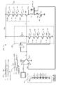
- Figure 3 schematically shows a voltage regulator according to an embodiment of the present invention;
- Figure 4 shows a flow-chart describing the operation of the voltage regulator according to an embodiment of the present invention; and
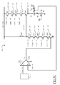
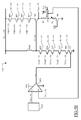
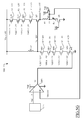
- Figures 5A-5G schematically show the voltage regulator of Figure 3 during the operation thereof according to an embodiment of the present invention.
- With reference in particular to Figure 1, a
non-volatile memory device 100 is schematically represented. Thememory device 100 includes one or more sectors 105 (only one shown in the Figure). Thesector 105 includes a plurality of memory cells MC, each one consisting of a floating gate MOS transistor. In particular, thememory device 100 is of the flash type, wherein the memory cells MC of thesector 105 must be erased at the same time. - The memory cells MC are arranged in rows and columns. The memory cells MC of each column have the drain terminals connected to a respective bit line BL, while the memory cells MC of each row have the gate terminals connected to a respective word line WL. The source terminals of all the memory cells MC are maintained at a reference voltage GND (or ground).
- The
memory device 100 receives an addressing code ADD for accessing the memory cells MC. A portion of the addressing code ADD is supplied to acolumn decoder 125, which selects a set of desired bit lines BL (such as 8). Another portion of the addressing code ADD is supplied to arow decoder 130, which selects one desired word line WL. - The
column decoder 125 couples the selected bit lines BL to a read-write circuit 135. The read/write circuit 135 includes all the components (e.g., sense amplifiers, comparators, reference current/voltage generators, pulse generators, program loads, and the like), which are normally required for writing desired logical values into the selected memory cells MC and for reading the logical values currently stored therein. The read/write circuit 135 is coupled with externally accessible terminals of the memory device 100 (not shown in figure) for receiving/delivering data. - The
memory device 100 further includes aPower Management Unit 140. ThePMU 140 provides the biasing voltages that are used for performing the conventional operations (such as read, program, erase and verify) on thememory device 100. For this purpose, thePMU 140 includes a boosting circuit - typically implemented by a charge pump 145 - which receives a supply voltage Vdd of the memory device 100 (such as 1.8-3V) from the outside and outputs different operative voltages Vhv; the operative voltages Vhv are generally higher in absolute value than the supply voltage Vdd (for example, ranging from -9V to 18V). Thecharge pump 145 is coupled with avoltage regulator 150, which outputs regulated voltages Vreg (being obtained by stabilizing the operative voltages Vhv). - Operation of the
flash memory 100 is managed by amicro-controller 155. Particularly, themicro-controller 155 includes acontrol unit 160 providing control signals (referred to as a whole with Sc), which are used for driving the various components of thememory device 100. Thecontrol unit 160 uses aRAM 165 as a working memory. Operation of thecontrol unit 160 is controlled by a low-level software program (or firmware), which is stored in aROM 170. - Referring to Figure 2, a conventional implementation of the
voltage regulator 150 is schematically represented. Thevoltage regulator 150 includes adifferential amplifier 205, which is supplied between the ground voltage GND and the operative voltage Vhv. Thedifferential amplifier 205 has a negative input terminal that receives a comparison reference voltage Vref (such as, 1V) from areference generator 215, and a positive input terminal that receives a feedback signal Vfb (as described in the following). An output terminal of thedifferential amplifier 205 generates a regulation signal Vr, which is applied to a control terminal of a regulation p-channel MOSFET Mp. The MOSFET Mp has a source terminal that is connected to an input terminal of the voltage regulator 150 (receiving the operative voltage Vhv), and a drain terminal that is connected to a reference terminal (providing the ground voltage GND) through aload resistor 210. A capacitor Cm is connected between the control terminal and the drain terminal of the MOSFET Mp, in order to reduce any fluctuations of the voltage at its drain terminal. The drain terminal of the MOSFET Mp provides an intermediate voltage Vi substantially at the desired value. The intermediate voltage Vi is applied to a control terminal of an output n-channel MOSFET Mn. The MOSFET Mn has a drain terminal that receives the operative voltage Vhv and a source terminal that is connected to a voltage divider. Particularly, the source terminal of the MOSFET Mn is connected to a first terminal of a resistor R1; a second terminal of the resistor R1 is connected to a first terminal of a potentiometer Rp, which has a second terminal connected to the reference terminal. The central tap of the voltage divider (i.e., between the resistor R1 and the potentiometer Rp) provides the feedback signal Vfb, which is returned to thedifferential amplifier 205. The source terminal of the MOSFET Mn defines an output terminal of thevoltage regulator 150, which provides the regulated voltage Vreg; particularly, the MOSFET Mn is connected in a voltage follower configuration so as to transfer the intermediate voltage Vi with reduced output impedance (thereby allowing driving high capacitive loads, not shown in the figure). - During the operation of the
voltage regulator 150, a negative feedback is established so that the feedback signal Vfb reaches a value substantially equal to the reference voltage Vref. In such condition, a current I flows through the potentiometer Rp, which current I has a value equal to the ratio between the reference voltage Vref and the resistance of the potentiometer Rp. Such current I also flows through the resistor R1 (since ideally no current flows in the positive input terminal of the differential amplifier 205) and through the MOSFET Mn. As a result, the regulated voltage Vreg is given by the following relation (hereinafter, the electrical quantities will be denoted with the same symbols used for the corresponding circuital elements):
- In such a way, by varying the resistance of the potentiometer Rp, it is possible to set the regulated voltage Vreg to any desired value below the operative voltage Vhv (for example ranging from 1V to 11V). The regulated voltage Vreg is stabilized with respect to any ripples of the operative voltage Vhv (for example, due to thermal phenomena). Indeed, if the operative voltage Vhv increases, the regulated voltage Vreg and the feedback signal Vfb increase accordingly. As a result, the regulation signal Vr increases; therefore, the voltage at the drain terminal of the MOSFET Mp decreases and brings back the regulated voltage Vreg to the desired value (by means of the MOSFET Mn). Similar considerations apply if the operative voltage Vhv decreases.
- As it can be noted, the
differential amplifier 205 is supplied by the operative voltage Vhv. Moreover, when the regulated voltage Vreg reaches low values (for example, 1-2V) the MOSFETs Mp and Mn receive high-voltages at their terminals. Therefore, in order to guarantee the correct operation of thevoltage regulator 150, its components must be implemented by high-voltage MOSFETs. - Referring now to Figure 3, an implementation of the voltage regulator according to an embodiment of the present invention (denoted with 1501) is schematically shown (wherein elements identical or similar to those shown in Figure 2 are denoted by the same reference numerals).
- In this case, the differential amplifier is replaced with an equivalent circuit (denoted with 2051), which is supplied between the supply voltage Vdd and the ground voltage GND (so that is can be implemented by means of low-voltage components only). Moreover, the regulation MOSFET Mp and the output MOSFET Mn are replaced by a regulation
circuital block 305 and by anoutput circuital block 310, respectively. - In addition, the
voltage regulator 1501 further includes a (low-voltage) P-channel MOSFET Mforce that has a source terminal receiving the supply voltage Vdd, a drain terminal connected to the central tap of the voltage divider R1, Rp and a control terminal receiving a starting signal START_N. Moreover, a (low-voltage) n-channel MOSFET Mb is interposed between the potentiometer Rp and the reference terminal (with its drain terminal and source terminal connected to the potentiometer Rp and to the reference terminal, respectively); the MOSFET Mb has a control terminal that receives an activation signal BUF_N. - In detail, the regulation
circuital block 305 includes an n-channel MOSFET MS that has a source terminal connected to the reference terminal, and a control terminal connected to the output terminal of the differential amplifier 2051 (thus receiving the regulation signal Vr). The use of the MOSFET MS of the n-type (instead of one of the p-type as in the above described prior art) avoids any breaking thereof even with the low value of the regulation signal Vr (now up-limited by the supply voltage Vdd). - One or more (auxiliary) n-type MOSFETs MSi (with i = 1..5 in the example at issue) are connected in series to the drain terminal of the MOSFET MS. Particularly, each MOSFET MSi has a source terminal (referred to as node Si) connected to the drain terminal of a preceding MOSFET MSi-1, with the exception of the source terminal of the first MOSFET MS1 that is connected to the drain terminal of the MOSFET MS. The drain terminal of the last MOSFET MS5 is coupled with an input terminal of the voltage regulator 1501 (receiving the operative voltage Vhv) through a load resistor Rpup; the drain terminal of the MOSFET MS5 provides the intermediate voltage Vi. Each MOSFET MSi has a control terminal receiving a corresponding control signal VHSi. As it will be apparent in the following, the MOSFETs MSi are controlled so as to avoid their breaking for any value of the intermediate voltage Vi (and then of the regulated voltage Vreg).
- Likewise, the
output circuital block 310 includes an n-channel MOSFET MF that has a control terminal receiving the intermediate voltage Vi, and a source terminal connected to the output terminal of the voltage regulator 1501 (providing the regulated voltage Vreg). One or more (auxiliary) n-type MOSFETs MFj (with j = 1..4 in the example at issue) are connected in series to a drain terminal of the MOSFET MF. Particularly, each MOSFET MFj has a source terminal (referred to as node Fj), which is connected to the drain terminal of a preceding MOSFET MFj-1, with the exception of the source terminal of the first MOSFET MF1 that is connected to the drain terminal of the MOSFET MF. The drain terminal of the last MOSFET MF4 directly receives the operative voltage Vhv. Moreover, each MOSFET MFj has a control terminal receiving a corresponding control signal VHFj. As it will be apparent in the following, the MOSFETs MFj are controlled so as to avoid their breaking for any value of the operative voltage Vhv. - The control signals VHS1 - VHS5 and VHF1 - VHF4 are generate by properly partitioning (through a voltage divider 335) the operative voltage Vhv so as to obtain lower voltages V1 - V5. The voltages V1 - V5 are then feed to two
sets 340 of voltage switches that are adapted to generate (according to the state of corresponding signals ENABLE1 and ENABLE2), the control signals VHS1 - VHS5 and VHF1 - VHF4, respectively. Preferably, the voltage switches of each set 340 are implemented by means of low-voltage MOSFETs only, as described in the co-pending Patent Application No.EP06111477.3 - As better described in the following, during the operation of the
voltage regulator 1501, the regulated voltage Vreg may take different values, for example ranging from a minimum predetermined value Vmin (in the example at issue, 1V) to a maximum predetermined value Vmax (in the example at issue, 11V). For this purpose, the regulated voltage Vreg is increased from the minimum predetermined value Vmin to the maximum predetermined value Vmax in succession by a delta value ΔV equal to the supply voltage Vdd minus a threshold voltage Vgs of the MOSFETs (in the example at issue, ΔV = 3-1 = 2V). This feature ensures that during the increase of the regulated voltage Vreg (including any transient periods) each MOSFET is properly biased so as to sustain at its terminals at most the supply voltage Vdd. - When the regulated voltage Vreg reaches low values (down to the minimum value Vmin = 1V) the arrangement of the MOSFETs MF, MF1 - MF4 ensures that the voltages sustained by each MOSFET MF, MF1 - MF4 (at its terminals) are at most equal to the supply voltage Vdd (meaning that the
output circuital block 310 only includes low-voltage MOSFETs MF, MF1 - MF4). - In particular, the minimum number M of the MOSFETs MFi (connected in series to the MOSFET MF) depends substantially on the operative voltage Vhv (disregarding the minimum value Vmin of the regulated voltage Vreg) and the maximum voltage that may be sustained at the terminals of the MOSFETs MF, MF1 - MF4 (that is, the supply voltage Vdd). In particular, in order to avoid any breaking of the MOSFETs MF, MFj the following condition must be met:

Therefore, the number M of the MOSFETs MFj is given by:
In the example at issue (wherein Vhv=11V and Vdd=3V), we have M ≥ 14/3 -1 = 4. - Vice-versa, when the regulated voltage Vreg reaches high values (up to the maximum value Vmax = 11V) the arrangement of the MOSFETs MS, MS1 - MS5 ensures that the voltages sustained by each MOSFET MS, MS1 - MS5 (at its terminals) are at most equal to the supply voltage Vdd (meaning that the regulation circuital block 305 only includes low-voltage MOSFETs MS, MS1 - MS5).
- In particular, the minimum number N of the MOSFETs MSi (connected in series to the MOSFET MS) depends on the maximum value Vmax of the regulated voltage Vreg and the delta value ΔV = Vdd - Vgs (since a MOSFET MSi is required for each increase of the intermediate voltage Vi - and then of the regulated voltage Vreg - by the delta value ΔV). In particular, the following condition must be met:

Therefore, the number N of the MOSFETs MSi is given by:
In the example at issue, we then have N ≥ 11/(3 -1) -1 = 5. - Likewise, the capacitor Cm may be obtained by means of a minimum number J of series-connected low-voltage capacitors (implemented by means of corresponding low-voltage MOSFETs). In this case as well, the number J depends on the maximum value Vmax of the regulated voltage Vreg and the maximum voltage which may be sustained at the terminals of these low-voltage MOSFETs (i.e., the supply voltage Vdd). In particular, the following condition must be met:

Therefore, the number J of the low-voltage MOSFETs used to implement the capacitor Cm is given by:
In the example at issue, we have J > 14/3 = 5. - With reference now to Figure 4, there is shown a
method 400 disclosing the operation of the above-described voltage regulator according to an embodiment of the present invention. Themethod 400 starts at theblock 405 and then moves to theblock 410. At the beginning, the starting signal START_N and the activation signal BUF_N are at the ground voltage GND; moreover, each control signal VHSi is at the supply voltage Vdd and each control signal VHFj is at a value equal to j*Vdd (in the example at issue, the control signals VHF1 - VHF4 are 3V, 6V, 9V and 12V, respectively). - In this condition, as shown in Figure 5A, the MOSFET Mforce is on. Thus, the voltage at the positive input terminal of the
differential amplifier 2051 reaches the supply voltage Vdd (i.e., 3V). On the other hand, thedifferential amplifier 2051 has the negative input terminal that receives the reference voltage Vref equal to 1V. In such a way, the regulation voltage Vr reaches the supply voltage Vdd (since the voltage at the positive input terminal of thedifferential amplifier 2051 is significantly higher than the voltage of the negative input terminal thereof). In such biasing condition, the MOSFET MS turns on, and then the MOSFETs MS1-MS5 turn on as well. In such a way, the nodes S1 - S5 are brought to the ground voltage GND, with the intermediate voltage Vi that is equal to the ground voltage GND as well. At the same time, the MOSFET Mb is off. Therefore, no current flows through the potentiometer Rp and the resistor R1 so that the regulated voltage Vreg reaches the supply voltage Vdd. The MOSFETs MF, MF1 - MF4 are not conductive (since they are series-connected to the resistor R1). In this condition, each node Fj reaches a voltage at least equal to the control signal VHFj minus the threshold voltage of the MOSFET MFj. In the example at issue, the nodes F1 - F4 reach thevoltages voltage regulator 1501 starts from a well-defined condition for its correct functioning. - Returning to Figure 4, the
block 410 is followed by theblock 415, wherein the starting signal START_N is brought to the supply voltage Vdd. - In this condition, as shown in Figure 5B, the MOSFET Mforce turns off. The negative feedback so established forces the feedback signal Vfb to the same value of the reference voltage Vref (i.e., 1V). Since no current flows through the potentiometer Rp and the resistor R1 (being the MOSFET Mb off) the regulated voltage Vreg reaches the reference voltage Vref as well. The MOSFETs MF, MF1 - MF4 are again not conductive (since they are series-connected to the resistor R1), with the nodes Fj that remain at the same voltages of 2V, 5V, 8V and 11V, respectively. In this condition, the control terminal of the MOSFET MF (i.e., the intermediate voltage Vi) reaches at most the regulated voltage Vreg plus the threshold voltage of the MOSFET MF (in the example at issue, 1+1=2V). Therefore, the source terminal of each transistor MSi (i.e., the nodes S1- S5) are brought to the same voltage of 2V.
- Returning to Figure 4, the
block 415 is followed by theblock 420, wherein two parameters K and Vf are initialized. In particular, the parameter K is set to 2 and the parameter Vf is set to the value of the supply voltage Vdd. Then, themethod 400 moves to theblock 425, wherein the activation signal BUF_N is brought to the supply voltage Vdd. Themethod 400 then enters a loop that starts at theblock 430, wherein the parameter Vf is increased by the delta value ΔV (in the example at issue, ΔV=2V), that is Vf = 3+2 = 5V. Then, themethod 400 moves to theblock 435 wherein an index x (used as a counter) is initialized to 1. Thus, themethod 400 verifies at theblock 440 whether the control signal VHFx (starting from x = 1) is lower than the parameter Vf. In the positive case, the control signal VHFx is set to the parameter Vf at theblock 445, and the flow of activity descends intoblock 450; the same point is also reached fromblock 440 directly otherwise. In any case, a test is performed at theblock 450 for determining whether the value of the parameter x is lower than the number M (in the example at issue, M = 4). If such condition is verified, the activity flow moves to theblock 455, wherein the parameter x is incremented by one. Then, the method returns to theblock 440 for reiterating the above described operations (in the example at issue, verifying the values of the control signals VHF2 - VHF4). The loop ends when the verification of theblock 450 has a negative result (meaning that every MOSFET MFj receives a corresponding control signal VHFj that is at least equal to the value of the parameter Vf). In such case, the method continues to theblock 460, wherein the regulated voltage Vreg (starting from 1V) is increased by an amount equal to the delta value ΔV=2V, that is Vreg = 1V+2V=3V. - Then, the
method 400 moves to theblock 465 wherein a test is performed for determining whether the value of the parameter K is higher than the number N (in the example at issue, N=5). If such condition is not verified, the activity flow moves to theblock 470, wherein another index y (used as a counter) is initialized to the value of the parameter K (i.e., y=2). Themethod 400 then passes to theblock 485, wherein the control signal VHSy (starting from y = K) is increased by the delta value ΔV = 2V. A test is performed at theblock 490 for determining whether the value of the index y is lower than or equal to the number N. If such condition is not verified, themethod 400 moves at theblock 495 wherein the index y is incremented by one. Then themethod 400 returns to theblock 485 for reiterating the above described operations. In case of positive result, themethod 400 moves from theblock 490 to theblock 496, wherein the parameter K is incremented by one. Then, themethod 400 moves to theblock 497. The same point is also reached fromblock 465 directly when the parameter K is higher than the number N. Themethod 400 then moves to theblock 497, wherein it verifies whether the regulated voltage Vreg has reached (or exceeded) the maximum value Vmax. In case of positive result, themethod 400 ends at theblock 498; vice versa themethod 400 returns to theblock 430 for reiterating the above described operations. - The condition after the first iteration of the loop 430 - 497 is shown in Figure 5C. Particularly, the MOSFET Mforce turns off - so as not to affect the feedback loop any longer - and the MOSFET Mb turns on - so that a current now flows through the MOSFET Mb and the potentiometer Rp. At the same time, the control signal VHF1 (being the only one lower than the parameter Vf=5V) is brought to the same voltage of 5V. As above, the negative feedback so established forces the feedback signal Vfb to the same value of the reference voltage Vref (i.e., 1V). The current flowing through the potentiometer Rp also flows through the resistor R1 (no current flows through the MOSFET Mforce because it is off); therefore, by varying the value of the resistance of the potentiometer Rp it is possible to bring the regulated voltage Vreg to the desired value of 1+2=3V. The current from the voltage divider R1, Rp flows through the MOSFETs MF, MF1 - MF4 that are then conductive. In such condition, each node Fj reaches a voltage at most equal to the control signal VHFj minus the threshold voltage of the MOSFET MFj. In the example at issue, the nodes F1 - F4 reach the
voltages - Thereafter, the control signals VHS2 - VHS5 (being the parameter K=2) are increased by 2V, so as to be brought to 3+2=5V. A corresponding current flows through the load resistor Rpup, and then trough the MOSFETs MS, MS1 - MS5 (which are again conductive). As a result, each node Si reaches a voltage at most equal to the control signal VHSi minus the threshold voltage of the MOSFETs Msi. In the example at issue, the nodes S1 - S5 reach the
voltages - The condition after the second iteration of the loop is shown in Figure 5D. As above, the parameter Vf is increased to 5+2=7V, and then the control signals VHF1 - VHF2 are brought to the same voltage of 7V. The regulated voltage Vreg is now brought to 3+2=5V. The nodes F1 - F4 then reach the
voltages voltages - Likewise, at the third iteration of the loop (as shown in Figure 5E), the parameter Vf is increased to 7+2=9V, and then the control signals VHF1 - VHF2 are brought to the same voltage of 9V. The regulated voltage Vreg is now brought to 5+2=7V. The nodes F1 - F4 then reach the
voltages voltages - Continuing to Figure 5F, at the fourth iteration of the loop the parameter Vf is increased to 9+2=11V, and then the control signals VHF1 - VHF3 are brought to the same voltage of 11V. The regulated voltage Vreg is now brought to 7+2=9V. The nodes F1 - F4 then reach the
voltages voltages - At the end, at the fifth and last iteration of the loop (as shown in Figure 5G), the parameter Vf is increased to 11+2=13V, and then all the control signals VHF1 - VHF4 are brought to the same voltage of 13V. The regulated voltage Vreg is now brought to 9+2=11V (i.e., it reaches the maximum value Vmax defining the exit condition of the loop). All the nodes F1 - F4 and the intermediate voltage Vi then reach the same voltage of 12V. The parameter K is increased to 5+1=6, and then no further operation is required for the control signals VHSi - since the condition for dropping the corresponding blocks (i.e., y<N) is satisfied.
- In this way, the regulated voltage Vreg may be brought to any desired value (from the minimum value Vmin to the maximum value Vmax), by simply interrupting the above-described iterations of the loop at will. In any case (as in the example at issue, wherein the regulated voltage Vreg is to be brought to the maximum value Vmax), the regulated voltage Vreg is increased in succession by the delta value ΔV=2V at each iteration of the loop. In this way, as clearly shown in the Figures 5A-5G, in every condition all the MOSFETs of the proposed voltage regulator are subjected to voltage differences (between any pair of their terminals) that are at most equal to the supply voltage Vdd (i.e., 3 V); consequently, the whole voltage regulator may be implemented using low voltage MOSFETs only.
- Therefore, it is possible to reduce the area of the chip wherein the memory device is integrated.
- Moreover, it is now possible to use a single process (based on the processing steps and masks for the low-voltage MOSFETs) for manufacturing the memory device including this voltage regulator; this has a beneficial impact on the manufacturing process of the whole memory device.
- Naturally, in order to satisfy local and specific requirements, a person skilled in the art may apply to the solution described above many modifications and alterations. Particularly, although the present invention has been described with a certain degree of particularity with reference to preferred embodiment(s) thereof, it should be understood that various omissions, substitutions and changes in the form and details as well as other embodiments are possible; moreover, it is expressly intended that specific elements and/or method steps described in connection with any disclosed embodiment of the invention may be incorporated in any other embodiment as a general matter of design choice.
- Particularly, the numerical examples described above are merely illustrative and must not be interpreted in a limitative manner. Moreover, similar considerations apply if the voltage regulator has a different structure or includes equivalent components. In any case, the proposed technique may also be applied to negative voltages (by means of a dual structure).
- It should be noted that the same result may also be achieved with a different number of auxiliary transistors for the regulator transistor (down to a single one).
- Likewise, the voltage divider may be replaced with any equivalent structure; as above, a different number of auxiliary transistors for the output transistor may be used (down to a single one). In any case, a simplified implementation of the voltage regulator without the above-described output stage is contemplated.
- The concepts of the present invention are also applicable to MOSFETs capable of sustaining between each pair of their terminals a voltage difference (slightly) higher than the supply voltage.
- Alternatively, it is possible to exchange the p-type and n-type MOSFETs, to replace the MOSFETs with other types of transistors (such as bipolar transistors), or with equivalent electronic components.
- Similar considerations apply if the positions of the resistor and of the potentiometer are exchanged in the voltage divider; in any case, a simplified implementation wherein the regulated voltage can take a predefined value only is not excluded.
- Although reference has been made to a specific non-volatile memory device, the concepts of the present invention are also applicable to other memory devices (such as multilevel flash memories, EEPROMs or phase-change memories); in any case, the voltage regulator according to the present invention lends itself to be exploited in any other electronic device.
- Likewise, the same voltage regulator may be used for regulating whatever voltage.
- Moreover, the proposed solution lends itself to be implemented with an equivalent method (by using similar steps, removing some steps being not essential, or adding further optional steps - even in a different order). For example, at the beginning the minimum value for the regulated voltage may be set to a different value (up to the supply voltage) or the control signals may be initialized in a different way; moreover, it is possible to update the control signals with an equivalent algorithm at each iteration of the loop.
- In any case, nothing prevents incrementing the regulated voltage at each iteration of the loop by another value (up to the supply voltage).
- Alternatively, it is possible to enforce an equivalent start-up condition of the voltage regulator; however, this feature is not strictly necessary, and it may be omitted in a simplified implementation of the invention.
- Similar considerations apply if the software program (which may be used to implement each embodiment of the invention) causes the micro-controller to perform equivalent operations. In any case, the program may take any form suitable to be used by or in connection with any logic controller. Moreover, it is possible to provide the program on any micro-controller usable medium; the medium can be any element suitable to contain, store, communicate, propagate, or transfer the program. For example, the medium may be of the electronic, magnetic, optical, electromagnetic, infrared, or semiconductor type. In any case, the solution according to the present invention lends itself to be implemented with a hardware structure, or with a combination of software and hardware.
- It should be readily apparent that the proposed voltage regulator may be part of the design of an integrated circuit. The design may also be created in a programming language; moreover, if the designer does not fabricate chips or masks, the design may be transmitted by physical means to others. In any case, the resulting integrated circuit may be distributed by its manufacturer in raw wafer form, as a bare die, or in packages form. Moreover, the device may be integrated with other circuits in the same chip, or it may be mounted in intermediate products (such as mother boards). In any case, the integrated circuit is suitable to be used in complex systems (such as computers).
Claims (13)
- A voltage regulator (1501) integrated in a chip of semiconductor material having a first input terminal for receiving a first voltage (Vhv) and an output terminal for providing a regulated voltage (Vreg) being obtained from the first voltage, the regulator including:a differential amplifier (2051) for receiving a comparison voltage (Vref) and a feedback signal (Vfb) being a function of the regulated voltage, and for proving a regulation signal (Vr) according to a comparison between the comparison voltage and the feedback signal, the differential amplifier having a first supply terminal being coupled with a reference terminal for receiving a reference voltage and a second supply terminal,a regulation transistor (MS) having a control terminal for receiving the regulation signal, and a conduction first terminal and a conduction second terminal being coupled through loading means (Rpup) between the reference terminal and the first input terminal of the regulator, the second terminal of the regulation transistor being coupled with the output terminal of the regulator,characterized in that
the second supply terminal of the differential amplifier is coupled with a second input terminal of the regulator for receiving a second voltage (Vdd) being lower than the first voltage in absolute value, and wherein the regulator further includes a set of auxiliary transistors (MS1-MS5) being connected in series between the second terminal of the regulation transistor and the output terminal of the regulator, and control means (155) for controlling the auxiliary transistors according to the regulated voltage. - The regulator (1501) according to claim 1, further including an output transistor (MF) having a control terminal being coupled with the second terminal of the regulation transistor (MS) through the auxiliary transistors (MS1-MS5), a conduction first terminal being coupled with the reference terminal through a voltage divider (R1,Rp), the first terminal of the output transistor providing the regulated voltage (Vreg) and the voltage divider providing the feedback signal (Vfb), and a conduction second terminal being coupled with the first input terminal of the regulator through a set of further auxiliary transistors (MF1-MF4) being connected in series, the control means (155) being further adapted to control the further auxiliary transistors according to the first voltage.
- The regulator (1501) according to claim 1 or 2, wherein the differential amplifier (2051), the auxiliary transistors (MS1-MS5) and/or the further auxiliary transistors (MF1-MF4) are adapted to sustain at most the second voltage, the control means (155) controlling the auxiliary transistors and/or the further auxiliary transistors (MF1-MF4) further according to the second voltage (Vdd).
- The regulator (1501) according to any claim from 1 to 3, wherein each auxiliary transistor (MS1-MS5) and each further auxiliary transistor (MF1-MF4) consists of a MOSFET, the first terminal consisting of a source terminal and the second terminal consisting of a drain terminal.
- The regulator (1051) according to any claim from 2 to 4, wherein the voltage divider (R1,Rp) includes means (Rp) for selecting the regulated voltage, the control means (155) including means (165) for causing the means for selecting to set the regulated voltage to a minimum value at most equal to the second voltage and for setting a set of control signals (VHS1-VHS5) for the auxiliary transistors (MS1-MS5) to the second voltage and a set of further control signals (VHF1-VHF5) for the further auxiliary transistors (MF1-MF5) to values increasing from the second voltage by the second voltage moving away from the output transistor (MF), and means (165) for reiterating, until the regulated voltage (Vreg) reaches a chosen target value, the operations of causing the means for selecting to increase the regulated voltage by a delta value at most equal to the second voltage, of setting the further control signals lower than a parameter voltage equal to the regulated voltage plus the delta value to the parameter voltage, and of increasing the control signals by the delta value for the auxiliary transistors from a current one to a last one moving away from the regulation transistor (MS), the current auxiliary transistor being incremented by one at each iteration starting from the second one.
- The regulator (1051) according to claim 5, wherein the delta value is substantially equal to the second voltage (Vdd) minus a threshold voltage of each transistor.
- The regulator (1051) according to claim 5 or 6, wherein the control means (155) including means (165) for enforcing a start-up condition of the regulator by forcing the feedback signal (Vfb) to a value at most equal to the second voltage.
- A non-volatile memory device (100) including the voltage regulator (1501) of any claim from 1 to 7.
- The memory device (100) of claim 8, wherein the second voltage (Vdd) is a supply voltage of the memory device, the memory device further including boosting means (145) for generating the first voltage from the second voltage.
- A method (400) for operating the voltage regulator of any claim from 2 to 7, the method including the steps of:setting (415) the regulated voltage to a minimum value at most equal to the second voltage, and setting a set of control signals (VHS1-VHS5) for the auxiliary transistors (MS1-MS5) to the second voltage and a set of further control signals (VHF1-VHF5) for the further auxiliary transistors (MF1-MF5) to values increasing from the second voltage by the second voltage moving away from the output transistor, andreiterating, until the regulated voltage reaches a chosen target value (497), the operations of:increasing (460) the regulated voltage by a delta value at most equal to the second voltage,setting (430-455) the further control signals lower than a parameter voltage equal to the regulated voltage plus the delta value to the parameter voltage, andincreasing (465-496) the control signals by the delta value for the auxiliary transistors from a current one to a last one moving away from the regulation transistor, the current auxiliary transistor being incremented by one at each iteration starting from the second one.
- The method (400) according to claim 10, wherein the delta value is substantially equal to the second voltage (Vdd) minus a threshold voltage of each transistor.
- The method (400) according to claim 10 or 11, further including the step of:enforcing (410) a start-up condition of the regulator by forcing the feedback signal to a value at most equal to the second voltage.
- A software program (170) for performing the method (400) of any claim from 10 to 12 when the software program is executed on a logic controller (155).
Priority Applications (4)
| Application Number | Priority Date | Filing Date | Title |
|---|---|---|---|
| EP06119456.9A EP1892600B1 (en) | 2006-08-24 | 2006-08-24 | Voltage regulator for non-volatile memories implemented with low-voltage transistors |
| US11/605,209 US7499345B2 (en) | 2005-11-25 | 2006-11-27 | Non-volatile memory implemented with low-voltages transistors and related system and method |
| US11/605,193 US20070170979A1 (en) | 2005-11-25 | 2006-11-27 | Charge pump systems and methods |
| US11/844,470 US7777466B2 (en) | 2006-08-24 | 2007-08-24 | Voltage regulator or non-volatile memories implemented with low-voltage transistors |
Applications Claiming Priority (1)
| Application Number | Priority Date | Filing Date | Title |
|---|---|---|---|
| EP06119456.9A EP1892600B1 (en) | 2006-08-24 | 2006-08-24 | Voltage regulator for non-volatile memories implemented with low-voltage transistors |
Publications (2)
| Publication Number | Publication Date |
|---|---|
| EP1892600A1 true EP1892600A1 (en) | 2008-02-27 |
| EP1892600B1 EP1892600B1 (en) | 2016-07-27 |
Family
ID=37672247
Family Applications (1)
| Application Number | Title | Priority Date | Filing Date |
|---|---|---|---|
| EP06119456.9A Active EP1892600B1 (en) | 2005-11-25 | 2006-08-24 | Voltage regulator for non-volatile memories implemented with low-voltage transistors |
Country Status (2)
| Country | Link |
|---|---|
| US (1) | US7777466B2 (en) |
| EP (1) | EP1892600B1 (en) |
Cited By (2)
| Publication number | Priority date | Publication date | Assignee | Title |
|---|---|---|---|---|
| US7592849B2 (en) | 2006-03-17 | 2009-09-22 | Stmicroelectronics, S.R.L. | Level shifter for semiconductor memory device implemented with low-voltage transistors |
| EP2924878A1 (en) * | 2014-03-28 | 2015-09-30 | STMicroelectronics Srl | Amplifier stage |
Families Citing this family (9)
| Publication number | Priority date | Publication date | Assignee | Title |
|---|---|---|---|---|
| FR2879771B1 (en) * | 2004-12-16 | 2007-06-22 | Atmel Nantes Sa Sa | HIGH VOLTAGE REGULATING DEVICE COMPATIBLE WITH LOW VOLTAGE TECHNOLOGIES AND CORRESPONDING ELECTRONIC CIRCUIT |
| US8022770B1 (en) * | 2010-05-27 | 2011-09-20 | Skyworks Solutions, Inc. | System and method for preventing power amplifier supply voltage saturation |
| US8743626B2 (en) * | 2011-02-18 | 2014-06-03 | Synopsys, Inc. | Controlling a non-volatile memory |
| US8687302B2 (en) | 2012-02-07 | 2014-04-01 | Lsi Corporation | Reference voltage circuit for adaptive power supply |
| US8710901B2 (en) | 2012-07-23 | 2014-04-29 | Lsi Corporation | Reference circuit with curvature correction using additional complementary to temperature component |
| US8830618B2 (en) | 2012-12-31 | 2014-09-09 | Lsi Corporation | Fly height control for hard disk drives |
| CN105811905B (en) * | 2014-12-29 | 2019-05-03 | 意法半导体研发(深圳)有限公司 | Low dropout amplifier |
| US10424385B1 (en) * | 2018-08-28 | 2019-09-24 | Dell Products L. P. | Self-configuring integrated circuit device |
| KR102861394B1 (en) * | 2019-11-08 | 2025-09-18 | 프라운호퍼 게젤샤프트 쭈르 푀르데룽 데어 안겐반텐 포르슝 에. 베. | Control method of a driver circuit, driver circuit, system including driver circuit, and method for manufacturing an integrated circuit |
Citations (4)
| Publication number | Priority date | Publication date | Assignee | Title |
|---|---|---|---|---|
| EP0576774A1 (en) * | 1992-06-30 | 1994-01-05 | STMicroelectronics S.r.l. | Voltage regulator for memory devices |
| US5473277A (en) * | 1993-05-13 | 1995-12-05 | Fujitsu Limited | Output circuit for providing a finally adjustable voltage |
| WO1997005696A1 (en) | 1995-08-01 | 1997-02-13 | Information Storage Devices, Inc. | Fully differential output cmos power amplifier |
| US20030042971A1 (en) | 2001-09-04 | 2003-03-06 | Kohei Oikawa | Power supply circuit having value of output voltage adjusted |
Family Cites Families (2)
| Publication number | Priority date | Publication date | Assignee | Title |
|---|---|---|---|---|
| JP4029812B2 (en) * | 2003-09-08 | 2008-01-09 | ソニー株式会社 | Constant voltage power circuit |
| JP4805699B2 (en) * | 2006-03-14 | 2011-11-02 | 株式会社リコー | Semiconductor device |
-
2006
- 2006-08-24 EP EP06119456.9A patent/EP1892600B1/en active Active
-
2007
- 2007-08-24 US US11/844,470 patent/US7777466B2/en active Active
Patent Citations (4)
| Publication number | Priority date | Publication date | Assignee | Title |
|---|---|---|---|---|
| EP0576774A1 (en) * | 1992-06-30 | 1994-01-05 | STMicroelectronics S.r.l. | Voltage regulator for memory devices |
| US5473277A (en) * | 1993-05-13 | 1995-12-05 | Fujitsu Limited | Output circuit for providing a finally adjustable voltage |
| WO1997005696A1 (en) | 1995-08-01 | 1997-02-13 | Information Storage Devices, Inc. | Fully differential output cmos power amplifier |
| US20030042971A1 (en) | 2001-09-04 | 2003-03-06 | Kohei Oikawa | Power supply circuit having value of output voltage adjusted |
Cited By (3)
| Publication number | Priority date | Publication date | Assignee | Title |
|---|---|---|---|---|
| US7592849B2 (en) | 2006-03-17 | 2009-09-22 | Stmicroelectronics, S.R.L. | Level shifter for semiconductor memory device implemented with low-voltage transistors |
| EP2924878A1 (en) * | 2014-03-28 | 2015-09-30 | STMicroelectronics Srl | Amplifier stage |
| US9502115B2 (en) | 2014-03-28 | 2016-11-22 | Stmicroelectronics S.R.L. | Amplifier stage |
Also Published As
| Publication number | Publication date |
|---|---|
| US7777466B2 (en) | 2010-08-17 |
| EP1892600B1 (en) | 2016-07-27 |
| US20080054864A1 (en) | 2008-03-06 |
Similar Documents
| Publication | Publication Date | Title |
|---|---|---|
| US7777466B2 (en) | Voltage regulator or non-volatile memories implemented with low-voltage transistors | |
| US8130026B2 (en) | Booster circuit and voltage supply circuit | |
| CN1832034B (en) | Method and circuit for generating high voltage and semiconductor memory device having the same | |
| CN101364118B (en) | Regulator and high voltage generator | |
| US9753476B1 (en) | Voltage regulator with fast overshoot settling response | |
| CN108231099B (en) | Regulating circuit for partitioned memory block and operation method thereof | |
| EP1298673B1 (en) | Semiconductor memory which has reduced fluctuation of writing speed | |
| US8902678B2 (en) | Voltage regulator | |
| US20010012219A1 (en) | Voltage regulator circuit built in a semiconductor memory device | |
| KR100560822B1 (en) | Semiconductor Devices Generate Ripple-Free Internal Voltages | |
| US10726927B2 (en) | Semiconductor memory device | |
| US6292396B1 (en) | Method and device for the programming of an electrically programmable non-volatile memory for improved reliability | |
| KR100897286B1 (en) | Negative potential discharge circuit | |
| KR101618732B1 (en) | Multi-time programmable memory for power management ic | |
| US10930322B2 (en) | Regulator and memory device having the same | |
| US6937517B2 (en) | Clock regulation scheme for varying loads | |
| US7385852B2 (en) | Circuit for generating step-up voltage in non-volatile memory device | |
| KR100553715B1 (en) | Multi Level High Voltage Regulator | |
| CN114167929A (en) | Voltage generating circuit and electronic device | |
| KR100825021B1 (en) | Internal voltage generator | |
| US7348832B2 (en) | Dual-voltage generation system | |
| KR100449558B1 (en) | Charge pump circuit | |
| KR20090000379A (en) | High voltage generation circuit and flash memory device having same |
Legal Events
| Date | Code | Title | Description |
|---|---|---|---|
| PUAI | Public reference made under article 153(3) epc to a published international application that has entered the european phase |
Free format text: ORIGINAL CODE: 0009012 |
|
| AK | Designated contracting states |
Kind code of ref document: A1 Designated state(s): AT BE BG CH CY CZ DE DK EE ES FI FR GB GR HU IE IS IT LI LT LU LV MC NL PL PT RO SE SI SK TR |
|
| AX | Request for extension of the european patent |
Extension state: AL BA HR MK YU |
|
| 17P | Request for examination filed |
Effective date: 20080822 |
|
| AKX | Designation fees paid |
Designated state(s): DE |
|
| 17Q | First examination report despatched |
Effective date: 20081021 |
|
| RAP1 | Party data changed (applicant data changed or rights of an application transferred) |
Owner name: STMICROELECTRONICS SRL |
|
| RAP1 | Party data changed (applicant data changed or rights of an application transferred) |
Owner name: STMICROELECTRONICS SRL |
|
| REG | Reference to a national code |
Ref country code: DE Ref legal event code: R079 Ref document number: 602006049707 Country of ref document: DE Free format text: PREVIOUS MAIN CLASS: G05F0001560000 Ipc: G11C0005140000 |
|
| RIC1 | Information provided on ipc code assigned before grant |
Ipc: G11C 16/30 20060101ALI20151001BHEP Ipc: G05F 1/565 20060101ALI20151001BHEP Ipc: G11C 5/14 20060101AFI20151001BHEP |
|
| GRAP | Despatch of communication of intention to grant a patent |
Free format text: ORIGINAL CODE: EPIDOSNIGR1 |
|
| INTG | Intention to grant announced |
Effective date: 20151127 |
|
| GRAS | Grant fee paid |
Free format text: ORIGINAL CODE: EPIDOSNIGR3 |
|
| RAP1 | Party data changed (applicant data changed or rights of an application transferred) |
Owner name: STMICROELECTRONICS NV |
|
| RAP1 | Party data changed (applicant data changed or rights of an application transferred) |
Owner name: NUMONYX BV |
|
| RAP1 | Party data changed (applicant data changed or rights of an application transferred) |
Owner name: MICRON TECHNOLOGY, INC. |
|
| GRAA | (expected) grant |
Free format text: ORIGINAL CODE: 0009210 |
|
| AK | Designated contracting states |
Kind code of ref document: B1 Designated state(s): DE |
|
| REG | Reference to a national code |
Ref country code: DE Ref legal event code: R096 Ref document number: 602006049707 Country of ref document: DE |
|
| REG | Reference to a national code |
Ref country code: DE Ref legal event code: R097 Ref document number: 602006049707 Country of ref document: DE |
|
| PLBE | No opposition filed within time limit |
Free format text: ORIGINAL CODE: 0009261 |
|
| STAA | Information on the status of an ep patent application or granted ep patent |
Free format text: STATUS: NO OPPOSITION FILED WITHIN TIME LIMIT |
|
| 26N | No opposition filed |
Effective date: 20170502 |
|
| REG | Reference to a national code |
Ref country code: DE Ref legal event code: R082 Ref document number: 602006049707 Country of ref document: DE Representative=s name: HOEGER, STELLRECHT & PARTNER PATENTANWAELTE MB, DE |
|
| PGFP | Annual fee paid to national office [announced via postgrant information from national office to epo] |
Ref country code: DE Payment date: 20250827 Year of fee payment: 20 |