EP1892546A2 - A method of producing a slab type two-dimensional photonic crystal structure - Google Patents
A method of producing a slab type two-dimensional photonic crystal structure Download PDFInfo
- Publication number
- EP1892546A2 EP1892546A2 EP07253330A EP07253330A EP1892546A2 EP 1892546 A2 EP1892546 A2 EP 1892546A2 EP 07253330 A EP07253330 A EP 07253330A EP 07253330 A EP07253330 A EP 07253330A EP 1892546 A2 EP1892546 A2 EP 1892546A2
- Authority
- EP
- European Patent Office
- Prior art keywords
- substrate
- dielectric
- slab
- photonic crystal
- single crystal
- Prior art date
- Legal status (The legal status is an assumption and is not a legal conclusion. Google has not performed a legal analysis and makes no representation as to the accuracy of the status listed.)
- Withdrawn
Links
- 239000004038 photonic crystal Substances 0.000 title claims description 32
- 238000000034 method Methods 0.000 title claims description 25
- 239000000758 substrate Substances 0.000 claims abstract description 58
- 239000013078 crystal Substances 0.000 claims abstract description 35
- 238000005530 etching Methods 0.000 claims description 11
- 239000003989 dielectric material Substances 0.000 claims description 7
- 239000010408 film Substances 0.000 description 60
- 229910052751 metal Inorganic materials 0.000 description 17
- 239000002184 metal Substances 0.000 description 17
- 239000010410 layer Substances 0.000 description 14
- 230000003287 optical effect Effects 0.000 description 11
- VYPSYNLAJGMNEJ-UHFFFAOYSA-N silicon dioxide Inorganic materials O=[Si]=O VYPSYNLAJGMNEJ-UHFFFAOYSA-N 0.000 description 11
- ZOKXTWBITQBERF-UHFFFAOYSA-N Molybdenum Chemical compound [Mo] ZOKXTWBITQBERF-UHFFFAOYSA-N 0.000 description 10
- NBIIXXVUZAFLBC-UHFFFAOYSA-N Phosphoric acid Chemical compound OP(O)(O)=O NBIIXXVUZAFLBC-UHFFFAOYSA-N 0.000 description 10
- 229910052750 molybdenum Inorganic materials 0.000 description 10
- 239000011733 molybdenum Substances 0.000 description 10
- 238000005498 polishing Methods 0.000 description 10
- 239000010931 gold Substances 0.000 description 9
- 238000001039 wet etching Methods 0.000 description 9
- 239000003960 organic solvent Substances 0.000 description 8
- KRHYYFGTRYWZRS-UHFFFAOYSA-N Fluorane Chemical compound F KRHYYFGTRYWZRS-UHFFFAOYSA-N 0.000 description 7
- 239000000463 material Substances 0.000 description 7
- 238000004544 sputter deposition Methods 0.000 description 7
- 239000000853 adhesive Substances 0.000 description 6
- 230000001070 adhesive effect Effects 0.000 description 6
- 239000011651 chromium Substances 0.000 description 6
- 238000000206 photolithography Methods 0.000 description 6
- 239000012790 adhesive layer Substances 0.000 description 5
- 229910000147 aluminium phosphate Inorganic materials 0.000 description 5
- 229910052681 coesite Inorganic materials 0.000 description 5
- 229910052906 cristobalite Inorganic materials 0.000 description 5
- 229960002050 hydrofluoric acid Drugs 0.000 description 5
- 239000000377 silicon dioxide Substances 0.000 description 5
- 229910052682 stishovite Inorganic materials 0.000 description 5
- 229910052905 tridymite Inorganic materials 0.000 description 5
- 238000001312 dry etching Methods 0.000 description 4
- 230000000694 effects Effects 0.000 description 4
- 239000004744 fabric Substances 0.000 description 4
- 239000000203 mixture Substances 0.000 description 4
- VLTRZXGMWDSKGL-UHFFFAOYSA-N perchloric acid Chemical compound OCl(=O)(=O)=O VLTRZXGMWDSKGL-UHFFFAOYSA-N 0.000 description 4
- 239000000243 solution Substances 0.000 description 4
- WFKWXMTUELFFGS-UHFFFAOYSA-N tungsten Chemical compound [W] WFKWXMTUELFFGS-UHFFFAOYSA-N 0.000 description 4
- 229910052721 tungsten Inorganic materials 0.000 description 4
- 239000010937 tungsten Substances 0.000 description 4
- VYZAMTAEIAYCRO-UHFFFAOYSA-N Chromium Chemical compound [Cr] VYZAMTAEIAYCRO-UHFFFAOYSA-N 0.000 description 3
- GRYLNZFGIOXLOG-UHFFFAOYSA-N Nitric acid Chemical compound O[N+]([O-])=O GRYLNZFGIOXLOG-UHFFFAOYSA-N 0.000 description 3
- HEMHJVSKTPXQMS-UHFFFAOYSA-M Sodium hydroxide Chemical compound [OH-].[Na+] HEMHJVSKTPXQMS-UHFFFAOYSA-M 0.000 description 3
- 229910052782 aluminium Inorganic materials 0.000 description 3
- XAGFODPZIPBFFR-UHFFFAOYSA-N aluminium Chemical compound [Al] XAGFODPZIPBFFR-UHFFFAOYSA-N 0.000 description 3
- 239000007864 aqueous solution Substances 0.000 description 3
- LDDQLRUQCUTJBB-UHFFFAOYSA-O azanium;hydrofluoride Chemical compound [NH4+].F LDDQLRUQCUTJBB-UHFFFAOYSA-O 0.000 description 3
- 230000015572 biosynthetic process Effects 0.000 description 3
- 229910052804 chromium Inorganic materials 0.000 description 3
- PCHJSUWPFVWCPO-UHFFFAOYSA-N gold Chemical compound [Au] PCHJSUWPFVWCPO-UHFFFAOYSA-N 0.000 description 3
- 229910052737 gold Inorganic materials 0.000 description 3
- 229910017604 nitric acid Inorganic materials 0.000 description 3
- 238000000059 patterning Methods 0.000 description 3
- 229920002120 photoresistant polymer Polymers 0.000 description 3
- 238000007740 vapor deposition Methods 0.000 description 3
- VEXZGXHMUGYJMC-UHFFFAOYSA-N Hydrochloric acid Chemical compound Cl VEXZGXHMUGYJMC-UHFFFAOYSA-N 0.000 description 2
- HKVFISRIUUGTIB-UHFFFAOYSA-O azanium;cerium;nitrate Chemical compound [NH4+].[Ce].[O-][N+]([O-])=O HKVFISRIUUGTIB-UHFFFAOYSA-O 0.000 description 2
- 230000007547 defect Effects 0.000 description 2
- 239000010432 diamond Substances 0.000 description 2
- 229910003460 diamond Inorganic materials 0.000 description 2
- 239000007789 gas Substances 0.000 description 2
- GQYHUHYESMUTHG-UHFFFAOYSA-N lithium niobate Chemical compound [Li+].[O-][Nb](=O)=O GQYHUHYESMUTHG-UHFFFAOYSA-N 0.000 description 2
- 229920003986 novolac Polymers 0.000 description 2
- 229920005989 resin Polymers 0.000 description 2
- 239000011347 resin Substances 0.000 description 2
- VZGDMQKNWNREIO-UHFFFAOYSA-N tetrachloromethane Chemical compound ClC(Cl)(Cl)Cl VZGDMQKNWNREIO-UHFFFAOYSA-N 0.000 description 2
- 239000010409 thin film Substances 0.000 description 2
- DDFHBQSCUXNBSA-UHFFFAOYSA-N 5-(5-carboxythiophen-2-yl)thiophene-2-carboxylic acid Chemical compound S1C(C(=O)O)=CC=C1C1=CC=C(C(O)=O)S1 DDFHBQSCUXNBSA-UHFFFAOYSA-N 0.000 description 1
- WSMQKESQZFQMFW-UHFFFAOYSA-N 5-methyl-pyrazole-3-carboxylic acid Chemical compound CC1=CC(C(O)=O)=NN1 WSMQKESQZFQMFW-UHFFFAOYSA-N 0.000 description 1
- DKNPRRRKHAEUMW-UHFFFAOYSA-N Iodine aqueous Chemical compound [K+].I[I-]I DKNPRRRKHAEUMW-UHFFFAOYSA-N 0.000 description 1
- WHXSMMKQMYFTQS-UHFFFAOYSA-N Lithium Chemical compound [Li] WHXSMMKQMYFTQS-UHFFFAOYSA-N 0.000 description 1
- ISWSIDIOOBJBQZ-UHFFFAOYSA-N Phenol Chemical compound OC1=CC=CC=C1 ISWSIDIOOBJBQZ-UHFFFAOYSA-N 0.000 description 1
- 230000005697 Pockels effect Effects 0.000 description 1
- 239000002253 acid Substances 0.000 description 1
- 230000015556 catabolic process Effects 0.000 description 1
- 238000012668 chain scission Methods 0.000 description 1
- 238000006731 degradation reaction Methods 0.000 description 1
- 230000002542 deteriorative effect Effects 0.000 description 1
- 239000003822 epoxy resin Substances 0.000 description 1
- 229910000040 hydrogen fluoride Inorganic materials 0.000 description 1
- 238000002347 injection Methods 0.000 description 1
- 239000007924 injection Substances 0.000 description 1
- 239000012212 insulator Substances 0.000 description 1
- 229910052744 lithium Inorganic materials 0.000 description 1
- 230000000737 periodic effect Effects 0.000 description 1
- 238000007517 polishing process Methods 0.000 description 1
- 229920000647 polyepoxide Polymers 0.000 description 1
- 229920000642 polymer Polymers 0.000 description 1
- 239000010453 quartz Substances 0.000 description 1
- 239000004065 semiconductor Substances 0.000 description 1
- 239000007787 solid Substances 0.000 description 1
- 239000006104 solid solution Substances 0.000 description 1
- PBCFLUZVCVVTBY-UHFFFAOYSA-N tantalum pentoxide Inorganic materials O=[Ta](=O)O[Ta](=O)=O PBCFLUZVCVVTBY-UHFFFAOYSA-N 0.000 description 1
- RIUWBIIVUYSTCN-UHFFFAOYSA-N trilithium borate Chemical compound [Li+].[Li+].[Li+].[O-]B([O-])[O-] RIUWBIIVUYSTCN-UHFFFAOYSA-N 0.000 description 1
Images


Classifications
-
- G—PHYSICS
- G02—OPTICS
- G02B—OPTICAL ELEMENTS, SYSTEMS OR APPARATUS
- G02B6/00—Light guides; Structural details of arrangements comprising light guides and other optical elements, e.g. couplings
- G02B6/10—Light guides; Structural details of arrangements comprising light guides and other optical elements, e.g. couplings of the optical waveguide type
- G02B6/12—Light guides; Structural details of arrangements comprising light guides and other optical elements, e.g. couplings of the optical waveguide type of the integrated circuit kind
- G02B6/122—Basic optical elements, e.g. light-guiding paths
- G02B6/1225—Basic optical elements, e.g. light-guiding paths comprising photonic band-gap structures or photonic lattices
-
- B—PERFORMING OPERATIONS; TRANSPORTING
- B82—NANOTECHNOLOGY
- B82Y—SPECIFIC USES OR APPLICATIONS OF NANOSTRUCTURES; MEASUREMENT OR ANALYSIS OF NANOSTRUCTURES; MANUFACTURE OR TREATMENT OF NANOSTRUCTURES
- B82Y20/00—Nanooptics, e.g. quantum optics or photonic crystals
-
- G—PHYSICS
- G02—OPTICS
- G02B—OPTICAL ELEMENTS, SYSTEMS OR APPARATUS
- G02B6/00—Light guides; Structural details of arrangements comprising light guides and other optical elements, e.g. couplings
- G02B6/10—Light guides; Structural details of arrangements comprising light guides and other optical elements, e.g. couplings of the optical waveguide type
- G02B6/12—Light guides; Structural details of arrangements comprising light guides and other optical elements, e.g. couplings of the optical waveguide type of the integrated circuit kind
Definitions
- the present invention relates to a method of producing a slab type two-dimensional photonic crystal structure.
- An optical device utilizing a photonic crystal has a structure of repeating different kinds of dielectric materials having different dielectric constants. According to such devices, the internal multiple reflection phenomenon is utilized to provide various kinds of devices having superior functions and of very small sizes. Since the principle of function of the device is based on multiple reflection phenomenon, the device properties have a strong dependency on frequency (wavelength) in the vicinity of a specific frequency. The frequency is decided upon the material (refractive index N) of a substrate for a photonic crystal and a length d of period of repetition of the photonic crystal structure. The dependency of the device on frequency is characteristic to the device. However, in the case that the device is used in a wide range of wavelength, the characteristics would turn to be a defect.
- an optical waveguide structure fabricated in a two-dimensional and triangle lattice photonic crystal can be easily produced, so that its practical application has been extensively investigated. It is, however, difficult to from many spaces or through holes in regularly positioned manner, so that the productivity is low. Further, it is more difficult to form many fine through holes or spaces in a dielectric single crystal having a high hardness at a high precision. In the case that the precision is low, the slab-type and two-dimensional photonic crystal structure would not provide desired electro-optic effects.
- An object of the present invention is to provide a method of forming many through holes at a high precision in producing a slab-type two-dimensional photonic crystal structure having a slab of a dielectric single crystal and lattice columns composed of the through holes.
- the present invention provides a method of producing a slab type two-dimensional photonic crystal structure having a slab of a dielectric single crystal and a lattice column having through holes formed therein.
- the method has the steps of:
- the inventors have reached an idea of providing recesses on a first main face of a substrate of a dielectric single crystal by etching and of mechanically processing the substrate at its second main face so that the recesses are opened to the side of the second main face to form through holes. It is possible to carry out the technique of forming many recesses at a regular interval by etching in the substrate of dielectric single crystal, at a high precision and high productivity. After many recesses are formed in the substrate at a regular interval, the substrate is mechanically processed at the second main face so that the recesses pass through the substrate to form the through holes. The precision of the thus obtained through hole is substantially decided upon the precision of the corresponding recess. It is thus possible to form many through holes at a high precision and high productivity. The precision and productivity of the slab-type and two-dimensional crystal structure can be thereby improved and its practical applicability can be considerably improved. The present invention is thus useful in the industry.
- a photonic crystal is a multi-dimension and periodic structure having a periodicity comparable with a wavelength of light with a plurality of media having different refractive indices.
- the photonic crystal has a band structure of light similar to that of electron. Specific structure thus provides photonic band gap of light.
- the photonic crystal having the photonic band gap functions as an insulator of light.
- Linear defects can be introduced into a photonic crystal having photonic band-gap for deteriorating its periodicity. It is thereby possible to form waveguide mode in a frequency region of the band-gap and to provide an optical waveguide confining light.
- a slab-type two-dimensional photonic crystal 15 is defined as follows. That is, to a dielectric slab, low dielectric pillars are provided at an appropriate two-dimensional period. Each dielectric pillar has a refractive index lower than that of the dielectric slab and has a shape of a column or an equilateral polygon.
- the dielectric slab is provided between a upper clad and a lower clad to provide the photonic crystal.
- the upper and lower clads have a refractive index lower than that of the dielectric slab.
- the method of forming an optical waveguide in the crystal is not particularly limited.
- so-called oxide clad two-dimensional slab-type photonic crystal is preferable because it is possible to easily produce the crystal of a large area.
- the oxide clad two-dimensional type photonic crystal is produced as follows. A thin film of a semiconductor of a high refractive index (refractive index of about 3 to 3.5) is formed on a dielectric material (oxide or polymer) of a low refractive index, in which a two-dimensional photonic crystal structure is fabricated.
- the upper and lower clads of the photonic crystal are composed of air layers.
- the dielectric single crystal includes quartz, lithium niobate single crystal, lithium tantalate single crystal, single crystal of lithium niobate-lithium tantalate solid solution, lithium borate single crystal and langasite single crystal.
- the substrate of the dielectric single crystal may be either of a Z-plate, X-plate (Y-plate) or the off-set plate of Z-plate or X-plate (Y-plate).
- the through holes are arranged to form regular lattices.
- shape of the lattice is not particularly limited, triangular lattice and regular quadratic lattice are listed.
- air filled in the through holes is a kind of a dielectric material so that the through holes can function as the dielectric pillars.
- solid or gaseous dielectric material other than air may be filled into the through holes to form the dielectric pillars each filled with the material.
- a substrate 1 for example a wafer
- a metal film 2 is formed on the whole of a first main face 1a of the substrate 1.
- the kind of the metal film is not particularly limited as far as it has resistance against an etchant or a etching gas of the substrate, it may be listed multilayered films of underlying Cr layer and Au layer laminated thereon, multilayered films of underlying Ti layer and Au layer laminated thereon, tungsten film and molybdenum film.
- the method of film formation is not particularly limited, and sputtering and vapor deposition are listed.
- the method of etching the metal film 2 and the substrate 1 of dielectric single crystal is not particularly limited, and includes dry etching and wet etching Wet etching is preferred.
- aqueous solution of iodine and potassium iodide is preferred as an etchant for gold
- aqueous solution of ammonium cerium nitrate and perchloric acid is preferred as an etchant for chromium.
- aqueous solution of ammonium cerium nitrate, perchloric acid and hydrochloric acid is preferred.
- Cl 2 is preferred as an etchant for gold
- mixture of CCl 4 and O 2 is preferred as an etchant for chromium.
- the etchant includes solution of hydrogen fluoride, solution of ammonium hydrogen fluoride, buffered fluoric acid solution (mixture of ammonium hydrogen fluoride and ammonium fluoride), solution of sodium hydroxide and the like.
- the etching gas includes CF 4 , SF 6 and the like.
- a resist 3 is formed on the metal film 2 (Fig. 1 (b)).
- the method of forming the resist 3 is not limited, and includes photolithography using a stepper.
- the metal film 2 and dielectric single crystal 1 are then etched by dry etching or wet etching to form recesses 4 (Fig. 1 (c)).
- Unnecessary resist 3 is then removed with an organic solvent (Fig. 1 (d)).
- the metal film 2A is removed to obtain a substrate 1 of a dielectric single crystal 1 with the recesses 4 formed therein, as shown in Fig. 1 (e).
- molybdenum film can be removed with mixed acid of nitric acid and phosphoric acid.
- the patterning of the resist can be performed by conventional exposure process.
- a contact aligner may be used upon the exposure.
- the material of the resist is needed to be resistive against the etchant for the metal film.
- Such material includes novolak resin type positive resist, main-chain scission (degradation) type positive resist, cyclized polyisoprene-azide compound series negative resist, phenol resin-azide compound series negative resist, dissolution-inhibition type electron rays positive resist and cross-linked type negative resist.
- a metal film 6 is formed on a first main face 5a of the base body 5 for supporting the dielectric slab.
- the kind of the metal film on the base body is not particularly limited, and includes multilayered films of underlying Cr layer and Au layer laminated thereon, multilayered films of underlying Ti layer and Au layer laminated thereon, tungsten film and molybdenum film.
- the method of film formation is not particularly limited, and sputtering and vapor deposition are listed.
- a resist 7 is then formed on the metal film 6 (Fig. 2 (b)). Photolithography and wet etching are applied to perform the patterning of the metal film to form a guard film 6A (Fig. 2 (c)). Unnecessary resist 7 is then removed with an organic solvent.
- a temporary supporting film 8 is formed on the base body 5 and the guard film 6A.
- the supporting film 8 is to be removed at the subsequent step to make the thin film of the dielectric single crystal distant from the underlying base body.
- a second main face 5b of the base body is then fixed on a polishing jig for forming a face for adhesion with the substrate of the dielectric single crystal.
- the temporary supporting film is then ground until the supporting film on the guard film disappears (Fig. 5 (c)).
- the material of the supporting film is not particularly limited, SiO 2 Ta 2 O 5 and Ti are listed. Further, although the material of the guard film is not particularly limited as far as it has resistance against an etchant for the temporary supporting film, molybdenum and tungsten can be listed.
- the method of grinding the temporary supporting film and the guard film is not particularly limited, loose abrasive and polishing pad of unwoven cloth sheet may be listed.
- the substrate 1 of dielectric single crystal is then ground at the main face 1b so that the recesses are opened to both of the main faces. That is, as shown in Fig. 3 (a), the guard film 6A and the supporting film 8 of the base body 5 are opposed to the main face 1a of the substrate 1.
- An adhesive is then interposed between them and cured to form an adhesive layer 9.
- the kind of the adhesive is not particularly limited, and includes a ultraviolet curable adhesive and a thermal curable adhesive.
- the second main face 5b of the base body 5 is adhered to and fixed on a polishing jig.
- the second main face 1b of the substrate 1 is then ground using a grinder and fixed abrasive to reduce the thickness of the substrate 1.
- the ground main face of the substrate 1 is subsequently polished so that the substrate 1 is further thinned.
- the substrate is finished using loose abrasive and polishing pad of unwoven cloth sheet to form a slab 10 of dielectric single crystal. Many through holes 11 are regularly formed in the slab 10 (Fig. 3 (b)).
- the method of the mechanical processing may preferably be, but not limited to, the grinding and polishing described above.
- the kind of the polishing process may preferably be, but not limited to, polishing using diamond abrasive.
- the final thickness of the dielectric slab is not limited, and is decided depending on the specification of a target slab-type and two dimensional photonic crystal structure. However, as an example, the thickness of the dielectric slab may preferably be 0.1 to 1.0 ⁇ m.
- etchant is flown through the through holes 11 formed in the dielectric slab 10.
- etchant is not limited and includes hydrofluoric acid and ammonium hydrogen fluoride.
- the adhesive layer 9A is removed as shown in Fig. 3 (c) and the supporting film 8 is removed by this etching process to form a space 12 (Fig. 3 (d)).
- spaces are provided over and under the dielectric slab 11 , which functions as a device having the slab-type and two-dimensional photonic crystal structure.
- a metal film 14 is formed over the whole of the polished face, as shown in Fig. 4 (a).
- the metal film 14 is also formed direct under the through hole 11.
- the kind of the metal film 14 is not particularly limited, and includes multilayered films of underlying Cr layer and Au layer laminated thereon, multilayered films of underlying Ti layer and Au layer laminated thereon, aluminum film and tungsten film.
- the method of forming the metal film 14 is not particularly limited, and sputtering and vapor deposition are listed.
- the metal film is then patterned by conventional photolithography and subjected to wet etching to from the target electrode pattern 14A and to remove the electrode 14 on the substrate 5 (Fig. 4 (c)). Unnecessary resist 15 is then removed with an organic solvent to obtain a slab-type and two-dimensional photonic crystal structure 16A, as shown in Fig. 5.
- a dielectric material is filled in the through holes 11 to provide dielectric pillars 18 shown in Fig. 6.
- Such dielectric material includes novolak resin and epoxy resin.
- the number of the through holes 11 between the electrode 14A and optical waveguide region may be increased. This kind of design is not particularly limited and may be variously changed.
- the thickness of the slab may preferably be 5 ⁇ m or smaller and more preferably be 3 ⁇ m or smaller.
- the optical waveguide structure of the present invention may be applied to various kinds of functional devices. That is, in addition to conventional optical waveguide, the optical waveguide structure may be applied to a device utilizing Pockels effect, a device utilizing plasma effect caused by injection of current, a device utilizing EO effects due to quantum well structure, a device utilizing TO effects due to change of heater temperature, a directional coupler, Mach-Zehnder optical waveguide and an optical modulator.
- the structure of the present invention is effective for electromagnetic waves. It is thus possible to obtain similar results as those of light wave in other electromagnetic waves by adjusting the material of the substrate and the period length "d".
- electromagnetic waves include microwave and terahertz wave.
- the slab-type and two-dimensional photonic crystal structure 16A was produced according to the procedure described above referring Figs. 1 to 5.
- the recesses 4 were formed in the dielectric substrate 1, according to the procedure described above referring to Fig. 1. Specifically, it was prepared a circular wafer 1 made of lithium niobate single crystal having a thickness of 0.5 mm and a diameter of 3 inches. A molybdenum film 2 of a thickness of 0.1 ⁇ m was formed by sputtering as a mask over the whole of the first main face 1a of the dielectric substrate 1. The molybdenum film 2 was subjected to patterning by photolithography using a stepper and dry etching to produce a mask 2A.
- the dielectric substrate 1 was then etched by wet etching using buffered fluoric acid heated at 65 ° C to a thickness of 1 ⁇ m. Unnecessary resist 3 was removed with an organic solvent, and the mask 2A of molybdenum was removed with mixture of nitric acid and phosphoric acid, as shown in Fig. 1 (e)).
- a molybdenum film 6 was formed by sputtering to a thickness of 2 ⁇ m over the whole of the first main face 5a of the base body 5, for supporting the dielectric slab.
- the molybdenum film was then patterned by conventional photolithography and wet etching to form a guard film 6A. Mixture of nitric acid and phosphoric acid heated at 40 ° C was used for the wet etching.
- Unnecessary resist 7 was then removed with an organic solvent and SiO 2 film was formed by sputtering at a thickness of 2.5 ⁇ m. The SiO 2 film was removed with buffered phosphoric acid in the subsequent step so that a space is formed between the dielectric slab and the base body.
- the second face 5b of the base body 5 was then fixed on a polishing jig for forming a face for adhesion with the dielectric substrate.
- the laminated films of SiO 2 and molybdenum were then ground to a thickness of 1.5 ⁇ m using loose abrasive and polishing pad of unwoven cloth sheet (Fig. 2 (e)).
- An organic adhesive forming an adhesive layer was applied on the main face 5a of the base body 5, and the main face 5a was adhered to the main face 1a of the substrate 1 with the recesses formed thereon.
- a pressure was applied onto the base body 5 and the dielectric substrate 1 with a pressing machine so that the thickness of the adhesive layer was reduced to 0.4 ⁇ m.
- the body 5 and substrate 1 were held in atmosphere at 200 ° C for 1 hour to solidify the adhesive so that the base body and the dielectric substrate were adhered with each other.
- the second main face 5b of the base body was adhered to and fixed on a polishing jig.
- the second main face 1b of the dielectric substrate 1 was ground with a grinder having fixed abrasive so that the thickness of the dielectric substrate 1 was reduced to 50 ⁇ m. Further, the thus ground main face 1b of the dielectric substrate 1 was then polished with diamond abrasive to further reduce the thickness of the dielectric substrate 1 to 2 ⁇ m. Finally, the dielectric substrate 1 was finished with loose abrasive and polishing pad of unwoven cloth sheet to reduce the thickness to 0.5 ⁇ m so that the recesses were opened to both main faces to form the through holes 11 (Fig. 3 (b)).
- the thus integrated assembly was then immersed in buffered fluoric acid heated at 40 ° C to supply buffered fluoric acid through the through holes 11 formed by the grinding.
- the SiO 2 layer 8 on the base body 5 was thus removed (Fig. 3 (d)).
- the thus obtained slab-type and two-dimensional photonic crystal structure was proved to be available as a slab-type and two-dimensional photonic crystal device.
Landscapes
- Physics & Mathematics (AREA)
- Engineering & Computer Science (AREA)
- Optics & Photonics (AREA)
- Microelectronics & Electronic Packaging (AREA)
- General Physics & Mathematics (AREA)
- Chemical & Material Sciences (AREA)
- Nanotechnology (AREA)
- Life Sciences & Earth Sciences (AREA)
- Biophysics (AREA)
- Crystallography & Structural Chemistry (AREA)
- Optical Integrated Circuits (AREA)
- Optical Modulation, Optical Deflection, Nonlinear Optics, Optical Demodulation, Optical Logic Elements (AREA)
Abstract
Description
- The present invention relates to a method of producing a slab type two-dimensional photonic crystal structure.
- An optical device utilizing a photonic crystal has a structure of repeating different kinds of dielectric materials having different dielectric constants. According to such devices, the internal multiple reflection phenomenon is utilized to provide various kinds of devices having superior functions and of very small sizes. Since the principle of function of the device is based on multiple reflection phenomenon, the device properties have a strong dependency on frequency (wavelength) in the vicinity of a specific frequency. The frequency is decided upon the material (refractive index N) of a substrate for a photonic crystal and a length d of period of repetition of the photonic crystal structure. The dependency of the device on frequency is characteristic to the device. However, in the case that the device is used in a wide range of wavelength, the characteristics would turn to be a defect.
- An optical waveguide utilizing a slab-type and two-dimensional photonic crystal is described, for example, in the following documents.
Japanese patent publication No. 2005-172932A
Japanese patent publication No. 2003-156642A
Japanese patent publication No. 2005-70163A
Japanese patent publication No. 2002-350657A - For example, an optical waveguide structure fabricated in a two-dimensional and triangle lattice photonic crystal can be easily produced, so that its practical application has been extensively investigated. It is, however, difficult to from many spaces or through holes in regularly positioned manner, so that the productivity is low. Further, it is more difficult to form many fine through holes or spaces in a dielectric single crystal having a high hardness at a high precision. In the case that the precision is low, the slab-type and two-dimensional photonic crystal structure would not provide desired electro-optic effects.
- An object of the present invention is to provide a method of forming many through holes at a high precision in producing a slab-type two-dimensional photonic crystal structure having a slab of a dielectric single crystal and lattice columns composed of the through holes.
- The present invention provides a method of producing a slab type two-dimensional photonic crystal structure having a slab of a dielectric single crystal and a lattice column having through holes formed therein. The method has the steps of:
- forming recesses in a substrate of a dielectric single crystal by etching a first main face of the substrate of the dielectric single crystal; and
- forming a slab by mechanically processing a second main face of the substrate so that the recesses pass through the slab to form the through holes
- The inventors have reached an idea of providing recesses on a first main face of a substrate of a dielectric single crystal by etching and of mechanically processing the substrate at its second main face so that the recesses are opened to the side of the second main face to form through holes. It is possible to carry out the technique of forming many recesses at a regular interval by etching in the substrate of dielectric single crystal, at a high precision and high productivity. After many recesses are formed in the substrate at a regular interval, the substrate is mechanically processed at the second main face so that the recesses pass through the substrate to form the through holes. The precision of the thus obtained through hole is substantially decided upon the precision of the corresponding recess. It is thus possible to form many through holes at a high precision and high productivity. The precision and productivity of the slab-type and two-dimensional crystal structure can be thereby improved and its practical applicability can be considerably improved. The present invention is thus useful in the industry.
-
- Figs. 1(a), 1(b), 1(c), 1(d) and 1(e) are cross sectional views showing respective steps of forming
recesses 4 in a substrate 1 of a dielectric single crystal. - Fig. 2(a), 2(b), 2(c) 2(d) and 2(e) are cross sectional views showing respective steps of forming a
guard film 6A and atemporary supporting film 8 on abase substrate 5. - Fig. 3 (a), (b), (c) and (d) are cross sectional views showing the respective steps of forming through
holes 11 in the substrate of dielectric single crystal and of formingspaces 12 on the back side of the substrate 1. - Fig. 4(a), 4(b) and 4(c) are cross sectional views showing respective steps of forming an
electrode 14A on the substrate of dielectric single crystal of Fig. 3 (d). - Fig. 5 is a cross sectional view showing a slab-type and two-dimensional
photonic crystal structure 16A obtained according to the present invention. - Fig. 6 is a cross sectional view showing a slab-type and two-dimensional
photonic crystal structure 16B obtained according to the present invention. - Fig. 7 is a cross sectional view showing a slab-type and two-dimensional
photonic crystal structure 16C obtained according to the present invention. - A photonic crystal is a multi-dimension and periodic structure having a periodicity comparable with a wavelength of light with a plurality of media having different refractive indices. The photonic crystal has a band structure of light similar to that of electron. Specific structure thus provides photonic band gap of light. The photonic crystal having the photonic band gap functions as an insulator of light.
- Linear defects can be introduced into a photonic crystal having photonic band-gap for deteriorating its periodicity. It is thereby possible to form waveguide mode in a frequency region of the band-gap and to provide an optical waveguide confining light.
- A slab-type two-
dimensional photonic crystal 15 is defined as follows. That is, to a dielectric slab, low dielectric pillars are provided at an appropriate two-dimensional period. Each dielectric pillar has a refractive index lower than that of the dielectric slab and has a shape of a column or an equilateral polygon. The dielectric slab is provided between a upper clad and a lower clad to provide the photonic crystal. The upper and lower clads have a refractive index lower than that of the dielectric slab. - The method of forming an optical waveguide in the crystal is not particularly limited. For example, so-called oxide clad two-dimensional slab-type photonic crystal is preferable because it is possible to easily produce the crystal of a large area. The oxide clad two-dimensional type photonic crystal is produced as follows. A thin film of a semiconductor of a high refractive index (refractive index of about 3 to 3.5) is formed on a dielectric material (oxide or polymer) of a low refractive index, in which a two-dimensional photonic crystal structure is fabricated.
- Further, so-called air-bridge type two-dimensional slab photonic crystal may be applied. According to this type, the upper and lower clads of the photonic crystal are composed of air layers.
- The dielectric single crystal includes quartz, lithium niobate single crystal, lithium tantalate single crystal, single crystal of lithium niobate-lithium tantalate solid solution, lithium borate single crystal and langasite single crystal. The substrate of the dielectric single crystal may be either of a Z-plate, X-plate (Y-plate) or the off-set plate of Z-plate or X-plate (Y-plate).
- Further, it is necessary that the through holes are arranged to form regular lattices. Although the shape of the lattice is not particularly limited, triangular lattice and regular quadratic lattice are listed. Further, air filled in the through holes is a kind of a dielectric material so that the through holes can function as the dielectric pillars. Further, solid or gaseous dielectric material other than air may be filled into the through holes to form the dielectric pillars each filled with the material.
- The present invention will be described in detail, referring to the attached drawings.
First, as shown in Fig. 1(a), a substrate 1 (for example a wafer) of a dielectric single crystal is prepared. A metal film 2 is formed on the whole of a first main face 1a of the substrate 1. Although the kind of the metal film is not particularly limited as far as it has resistance against an etchant or a etching gas of the substrate, it may be listed multilayered films of underlying Cr layer and Au layer laminated thereon, multilayered films of underlying Ti layer and Au layer laminated thereon, tungsten film and molybdenum film. The method of film formation is not particularly limited, and sputtering and vapor deposition are listed. - The method of etching the metal film 2 and the substrate 1 of dielectric single crystal is not particularly limited, and includes dry etching and wet etching Wet etching is preferred.
- The method of etching the metal film itself is known. For example, aqueous solution of iodine and potassium iodide is preferred as an etchant for gold, and aqueous solution of ammonium cerium nitrate and perchloric acid is preferred as an etchant for chromium. Further, in the case that gold and chromium are etched at the same time, aqueous solution of ammonium cerium nitrate, perchloric acid and hydrochloric acid is preferred. In the case of dry etching, Cl2 is preferred as an etchant for gold and mixture of CCl4 and O2 is preferred as an etchant for chromium.
- The method itself of etching a dielectric single crystal is also known. For example, the etchant includes solution of hydrogen fluoride, solution of ammonium hydrogen fluoride, buffered fluoric acid solution (mixture of ammonium hydrogen fluoride and ammonium fluoride), solution of sodium hydroxide and the like. The etching gas includes CF4, SF6 and the like.
- Preferably, a resist 3 is formed on the metal film 2 (Fig. 1 (b)). The method of forming the resist 3 is not limited, and includes photolithography using a stepper. The metal film 2 and dielectric single crystal 1 are then etched by dry etching or wet etching to form recesses 4 (Fig. 1 (c)). Unnecessary resist 3 is then removed with an organic solvent (Fig. 1 (d)). The
metal film 2A is removed to obtain a substrate 1 of a dielectric single crystal 1 with therecesses 4 formed therein, as shown in Fig. 1 (e). For example, molybdenum film can be removed with mixed acid of nitric acid and phosphoric acid. - The patterning of the resist can be performed by conventional exposure process. A contact aligner may be used upon the exposure.
- The material of the resist is needed to be resistive against the etchant for the metal film. Such material includes novolak resin type positive resist, main-chain scission (degradation) type positive resist, cyclized polyisoprene-azide compound series negative resist, phenol resin-azide compound series negative resist, dissolution-inhibition type electron rays positive resist and cross-linked type negative resist.
- The method of processing the
base body 5 will be described.
As shown in Fig. 2 (a), ametal film 6 is formed on a firstmain face 5a of thebase body 5 for supporting the dielectric slab. The kind of the metal film on the base body is not particularly limited, and includes multilayered films of underlying Cr layer and Au layer laminated thereon, multilayered films of underlying Ti layer and Au layer laminated thereon, tungsten film and molybdenum film. The method of film formation is not particularly limited, and sputtering and vapor deposition are listed. - A resist 7 is then formed on the metal film 6 (Fig. 2 (b)). Photolithography and wet etching are applied to perform the patterning of the metal film to form a
guard film 6A (Fig. 2 (c)). Unnecessary resist 7 is then removed with an organic solvent. - A temporary supporting
film 8 is formed on thebase body 5 and theguard film 6A. The supportingfilm 8 is to be removed at the subsequent step to make the thin film of the dielectric single crystal distant from the underlying base body. A secondmain face 5b of the base body is then fixed on a polishing jig for forming a face for adhesion with the substrate of the dielectric single crystal. The temporary supporting film is then ground until the supporting film on the guard film disappears (Fig. 5 (c)). - Although the material of the supporting film is not particularly limited, SiO2 Ta2O5 and Ti are listed. Further, although the material of the guard film is not particularly limited as far as it has resistance against an etchant for the temporary supporting film, molybdenum and tungsten can be listed.
- Further, the method of grinding the temporary supporting film and the guard film is not particularly limited, loose abrasive and polishing pad of unwoven cloth sheet may be listed.
- The substrate 1 of dielectric single crystal is then ground at the main face 1b so that the recesses are opened to both of the main faces. That is, as shown in Fig. 3 (a), the
guard film 6A and the supportingfilm 8 of thebase body 5 are opposed to the main face 1a of the substrate 1. An adhesive is then interposed between them and cured to form anadhesive layer 9. The kind of the adhesive is not particularly limited, and includes a ultraviolet curable adhesive and a thermal curable adhesive. - After the
base body 5 is adhered with and fixed onto the substrate 1 of dielectric single crystal, the secondmain face 5b of thebase body 5 is adhered to and fixed on a polishing jig. The second main face 1b of the substrate 1 is then ground using a grinder and fixed abrasive to reduce the thickness of the substrate 1. The ground main face of the substrate 1 is subsequently polished so that the substrate 1 is further thinned. Finally, the substrate is finished using loose abrasive and polishing pad of unwoven cloth sheet to form aslab 10 of dielectric single crystal. Many throughholes 11 are regularly formed in the slab 10 (Fig. 3 (b)). - The method of the mechanical processing may preferably be, but not limited to, the grinding and polishing described above. Further, the kind of the polishing process may preferably be, but not limited to, polishing using diamond abrasive. Further, the final thickness of the dielectric slab is not limited, and is decided depending on the specification of a target slab-type and two dimensional photonic crystal structure. However, as an example, the thickness of the dielectric slab may preferably be 0.1 to 1.0 µm.
- From the state shown in Fig. 3 (b), the
adhesive layer 9 and temporary supportingfilm 8 under thedielectric slab 10 was removed by etching. That is, an etchant is flown through the throughholes 11 formed in thedielectric slab 10. Such etchant is not limited and includes hydrofluoric acid and ammonium hydrogen fluoride. - The
adhesive layer 9A is removed as shown in Fig. 3 (c) and the supportingfilm 8 is removed by this etching process to form a space 12 (Fig. 3 (d)). As a result, spaces are provided over and under thedielectric slab 11 , which functions as a device having the slab-type and two-dimensional photonic crystal structure. - After the polished face of the
dielectric slab 10 is washed with an organic solvent, ametal film 14 is formed over the whole of the polished face, as shown in Fig. 4 (a). Themetal film 14 is also formed direct under the throughhole 11. The kind of themetal film 14 is not particularly limited, and includes multilayered films of underlying Cr layer and Au layer laminated thereon, multilayered films of underlying Ti layer and Au layer laminated thereon, aluminum film and tungsten film. The method of forming themetal film 14 is not particularly limited, and sputtering and vapor deposition are listed. - The metal film is then patterned by conventional photolithography and subjected to wet etching to from the
target electrode pattern 14A and to remove theelectrode 14 on the substrate 5 (Fig. 4 (c)). Unnecessary resist 15 is then removed with an organic solvent to obtain a slab-type and two-dimensionalphotonic crystal structure 16A, as shown in Fig. 5. - Further, in the
device 16A shown in Fig. 5, a dielectric material is filled in the throughholes 11 to providedielectric pillars 18 shown in Fig. 6. Such dielectric material includes novolak resin and epoxy resin.
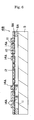
Further, as shown in adevice 16C of Fig. 7, the number of the throughholes 11 between theelectrode 14A and optical waveguide region may be increased. This kind of design is not particularly limited and may be variously changed. - Although the shape of the dielectric slab is not limited as far as a target electromagnetic wave can propagate in slab mode, the thickness of the slab may preferably be 5 µm or smaller and more preferably be 3 µm or smaller.
- The optical waveguide structure of the present invention may be applied to various kinds of functional devices.
That is, in addition to conventional optical waveguide, the optical waveguide structure may be applied to a device utilizing Pockels effect, a device utilizing plasma effect caused by injection of current, a device utilizing EO effects due to quantum well structure, a device utilizing TO effects due to change of heater temperature, a directional coupler, Mach-Zehnder optical waveguide and an optical modulator. - The structure of the present invention is effective for electromagnetic waves. It is thus possible to obtain similar results as those of light wave in other electromagnetic waves by adjusting the material of the substrate and the period length "d". Such electromagnetic waves include microwave and terahertz wave.
- The slab-type and two-dimensional
photonic crystal structure 16A was produced according to the procedure described above referring Figs. 1 to 5. - The
recesses 4 were formed in the dielectric substrate 1, according to the procedure described above referring to Fig. 1.
Specifically, it was prepared a circular wafer 1 made of lithium niobate single crystal having a thickness of 0.5 mm and a diameter of 3 inches. A molybdenum film 2 of a thickness of 0.1 µm was formed by sputtering as a mask over the whole of the first main face 1a of the dielectric substrate 1. The molybdenum film 2 was subjected to patterning by photolithography using a stepper and dry etching to produce amask 2A. - The dielectric substrate 1 was then etched by wet etching using buffered fluoric acid heated at 65 ° C to a thickness of 1 µm. Unnecessary resist 3 was removed with an organic solvent, and the
mask 2A of molybdenum was removed with mixture of nitric acid and phosphoric acid, as shown in Fig. 1 (e)). - A
molybdenum film 6 was formed by sputtering to a thickness of 2 µ m over the whole of the firstmain face 5a of thebase body 5, for supporting the dielectric slab. The molybdenum film was then patterned by conventional photolithography and wet etching to form aguard film 6A. Mixture of nitric acid and phosphoric acid heated at 40 ° C was used for the wet etching. Unnecessary resist 7 was then removed with an organic solvent and SiO2 film was formed by sputtering at a thickness of 2.5 µm. The SiO2 film was removed with buffered phosphoric acid in the subsequent step so that a space is formed between the dielectric slab and the base body. Further, Thesecond face 5b of thebase body 5 was then fixed on a polishing jig for forming a face for adhesion with the dielectric substrate. The laminated films of SiO2 and molybdenum were then ground to a thickness of 1.5 µm using loose abrasive and polishing pad of unwoven cloth sheet (Fig. 2 (e)). - An organic adhesive forming an adhesive layer was applied on the
main face 5a of thebase body 5, and themain face 5a was adhered to the main face 1a of the substrate 1 with the recesses formed thereon. A pressure was applied onto thebase body 5 and the dielectric substrate 1 with a pressing machine so that the thickness of the adhesive layer was reduced to 0.4 µm. Thebody 5 and substrate 1 were held in atmosphere at 200 ° C for 1 hour to solidify the adhesive so that the base body and the dielectric substrate were adhered with each other. - After the
base body 5 was adhered to and fixed on the dielectric substrate 1, the secondmain face 5b of the base body was adhered to and fixed on a polishing jig. The second main face 1b of the dielectric substrate 1 was ground with a grinder having fixed abrasive so that the thickness of the dielectric substrate 1 was reduced to 50 µm. Further, the thus ground main face 1b of the dielectric substrate 1 was then polished with diamond abrasive to further reduce the thickness of the dielectric substrate 1 to 2 µm. Finally, the dielectric substrate 1 was finished with loose abrasive and polishing pad of unwoven cloth sheet to reduce the thickness to 0.5 µm so that the recesses were opened to both main faces to form the through holes 11 (Fig. 3 (b)). - The thus integrated assembly was then immersed in buffered fluoric acid heated at 40 ° C to supply buffered fluoric acid through the through
holes 11 formed by the grinding. The SiO2 layer 8 on thebase body 5 was thus removed (Fig. 3 (d)). - After the thus polished face of the dielectric slab was washed with an organic solvent, aluminum film having a thickness of 0.02 µ m was formed over the whole of the polished face by sputtering (Fig. 4 (a)). The aluminum film was patterned by conventional photolithography and then subjected to wet etching using phosphoric acid etchant heated at 40 ° C to obtain target electrode pattern (Fig. 4 (b)). Unnecessary resist 15 was then removed with an organic solvent and the thus obtained assembly was cut into respective chips with a dicing saw. The photonic crystal device was thus obtained (Fig. 5).
- The thus obtained slab-type and two-dimensional photonic crystal structure was proved to be available as a slab-type and two-dimensional photonic crystal device.
Claims (3)
- A method of producing a slab type two-dimensional photonic crystal structure comprising a slab of a dielectric single crystal and a lattice column comprising through holes; said method comprising the steps of:forming recesses in a substrate of a dielectric single crystal by etching a first main face of said substrate of said dielectric single crystal; andforming a slab by mechanically processing a second main face of said substrate so that said recesses pass through said slab to form said through holes.
- The method of claim 1, further comprising the step of fixing said substrate on a base body at said first main face after said recesses are formed on said first main face of said substrate, wherein said mechanical processing is performed after said substrate is fixed onto said base body.
- The method of claim 1 or 2, further comprising the step of filling a dielectric material into said through holes to form dielectric pillars.
Applications Claiming Priority (1)
| Application Number | Priority Date | Filing Date | Title |
|---|---|---|---|
| JP2006229210A JP4785194B2 (en) | 2006-08-25 | 2006-08-25 | Method for manufacturing slab type two-dimensional photonic crystal structure |
Publications (2)
| Publication Number | Publication Date |
|---|---|
| EP1892546A2 true EP1892546A2 (en) | 2008-02-27 |
| EP1892546A3 EP1892546A3 (en) | 2008-03-12 |
Family
ID=38924411
Family Applications (1)
| Application Number | Title | Priority Date | Filing Date |
|---|---|---|---|
| EP07253330A Withdrawn EP1892546A3 (en) | 2006-08-25 | 2007-08-23 | A method of producing a slab type two-dimensional photonic crystal structure |
Country Status (3)
| Country | Link |
|---|---|
| US (1) | US8002998B2 (en) |
| EP (1) | EP1892546A3 (en) |
| JP (1) | JP4785194B2 (en) |
Cited By (1)
| Publication number | Priority date | Publication date | Assignee | Title |
|---|---|---|---|---|
| CN110045445A (en) * | 2018-01-15 | 2019-07-23 | 茂邦电子有限公司 | Have the optical plate and its manufacturing method of high-aspect-ratio light guide hole array |
Families Citing this family (9)
| Publication number | Priority date | Publication date | Assignee | Title |
|---|---|---|---|---|
| KR101175699B1 (en) * | 2011-03-16 | 2012-08-21 | 광주과학기술원 | Terahertz modulator based on hole injection and transport |
| JP6033196B2 (en) | 2013-10-08 | 2016-11-30 | 日本碍子株式会社 | Manufacturing method of optical components |
| JP2022553495A (en) * | 2019-10-18 | 2022-12-23 | カリフォルニア インスティチュート オブ テクノロジー | CMOS color image sensor with metamaterial color separation |
| DE112021001746T8 (en) * | 2020-05-28 | 2023-02-23 | Ngk Insulators, Ltd. | COMPOSITE SUBSTRATE FOR PHOTONIC CRYSTAL ELEMENTS AND PHOTONIC CRYSTAL ELEMENT |
| DE112021002832T5 (en) * | 2020-07-20 | 2023-03-02 | Ngk Insulators, Ltd. | Optical scanning element |
| DE112021003953T5 (en) * | 2020-07-27 | 2023-06-07 | Ngk Insulators, Ltd. | Photonic crystal element |
| WO2022162981A1 (en) * | 2021-02-01 | 2022-08-04 | 日本碍子株式会社 | Optical scanning element |
| DE112022000898T5 (en) * | 2021-03-29 | 2023-11-16 | Ngk Insulators, Ltd. | Waveguide element |
| DE112022002796T5 (en) * | 2021-08-10 | 2024-04-18 | Ngk Insulators, Ltd. | WAVEGUIDE ELEMENT |
Citations (1)
| Publication number | Priority date | Publication date | Assignee | Title |
|---|---|---|---|---|
| US20060034577A1 (en) | 2004-05-20 | 2006-02-16 | Matsushita Electric Industrial Co., Ltd. | Photonic crystal device |
Family Cites Families (14)
| Publication number | Priority date | Publication date | Assignee | Title |
|---|---|---|---|---|
| US5205902A (en) | 1989-08-18 | 1993-04-27 | Galileo Electro-Optics Corporation | Method of manufacturing microchannel electron multipliers |
| US6613241B1 (en) | 1999-10-29 | 2003-09-02 | California Insitute Of Technology | MEMS elements with integrated porous membranes and method of making the same |
| JP3800088B2 (en) | 2000-12-27 | 2006-07-19 | 日本電信電話株式会社 | Photonic crystal waveguide |
| DE60127730T2 (en) | 2000-12-27 | 2007-12-27 | Nippon Telegraph And Telephone Corp. | Photonic crystal waveguide |
| JP2003066858A (en) | 2001-08-23 | 2003-03-05 | Sony Corp | Method of manufacturing thin-film device substrate |
| JP3867848B2 (en) | 2001-09-07 | 2007-01-17 | 日本電信電話株式会社 | Optical waveguide |
| WO2004036265A2 (en) * | 2002-10-16 | 2004-04-29 | Lake Shore Cryotronics, Inc. | Spectral filter for green and longer wavelengths |
| DE10352590A1 (en) * | 2002-11-12 | 2004-05-27 | Toptica Photonics Ag | Method for manufacturing optical fibre with output point for stray light and measuring fibre optical power, with optical fibre contiguous core , and surrounding sleeve with second lower refraction index, while fibre section |
| US7215842B2 (en) * | 2003-04-18 | 2007-05-08 | Ricoh Company, Ltd. | Light control element and light control device |
| US7195715B2 (en) * | 2003-05-27 | 2007-03-27 | Citizen Watch Co., Ltd. | Method for manufacturing quartz oscillator |
| JP3876863B2 (en) | 2003-08-20 | 2007-02-07 | 日本電信電話株式会社 | Add-drop filter |
| US7333703B2 (en) | 2003-08-29 | 2008-02-19 | Kyoto University | Two-dimensional photonic crystal having air-bridge structure and method for manufacturing such a crystal |
| JP3886958B2 (en) | 2003-12-08 | 2007-02-28 | 国立大学法人京都大学 | Manufacturing method of two-dimensional photonic crystal with thin wire waveguide |
| JP4653393B2 (en) * | 2003-09-18 | 2011-03-16 | 株式会社リコー | Light control element |
-
2006
- 2006-08-25 JP JP2006229210A patent/JP4785194B2/en active Active
-
2007
- 2007-08-21 US US11/842,277 patent/US8002998B2/en not_active Expired - Fee Related
- 2007-08-23 EP EP07253330A patent/EP1892546A3/en not_active Withdrawn
Patent Citations (1)
| Publication number | Priority date | Publication date | Assignee | Title |
|---|---|---|---|---|
| US20060034577A1 (en) | 2004-05-20 | 2006-02-16 | Matsushita Electric Industrial Co., Ltd. | Photonic crystal device |
Cited By (2)
| Publication number | Priority date | Publication date | Assignee | Title |
|---|---|---|---|---|
| CN110045445A (en) * | 2018-01-15 | 2019-07-23 | 茂邦电子有限公司 | Have the optical plate and its manufacturing method of high-aspect-ratio light guide hole array |
| CN110045445B (en) * | 2018-01-15 | 2021-06-29 | 茂邦电子有限公司 | Light guide plate with high depth-width ratio light guide hole array and its making method |
Also Published As
| Publication number | Publication date |
|---|---|
| US20080047928A1 (en) | 2008-02-28 |
| JP4785194B2 (en) | 2011-10-05 |
| EP1892546A3 (en) | 2008-03-12 |
| JP2008052108A (en) | 2008-03-06 |
| US8002998B2 (en) | 2011-08-23 |
Similar Documents
| Publication | Publication Date | Title |
|---|---|---|
| US8002998B2 (en) | Method of producing a slab type two-dimensional photonic crystal structure | |
| JP4825847B2 (en) | Optical element and manufacturing method thereof | |
| EP2863545B1 (en) | Composite substrate | |
| JP5117126B2 (en) | Wafer scale method for manufacturing optical waveguide devices and waveguide devices manufactured thereby | |
| CN108710267B (en) | Preparation method of thin film micro-optical structure based on photoetching and chemical mechanical polishing | |
| WO2005114279A1 (en) | Photonic crystal device | |
| JP4174377B2 (en) | Optical element | |
| JP2002521711A (en) | Method for manufacturing an optical waveguide | |
| JPWO2006093056A1 (en) | Electromagnetic resonator, method of manufacturing the same, and electromagnetic resonance method | |
| JPH1010348A (en) | Production of optical waveguide device | |
| JP2003107545A (en) | Manufacturing method for ridge type optical waveguide element | |
| JP5234236B2 (en) | Quartz substrate and method for manufacturing quartz substrate | |
| JP4113478B2 (en) | Manufacturing method of two-dimensional photonic crystal optical device | |
| US20230188109A1 (en) | Method For Manufacturing Vibrator Element | |
| US20230179164A1 (en) | Method For Manufacturing Vibrator Element | |
| US9733546B2 (en) | Optical component | |
| JPH11352350A (en) | Production of optical waveguide element | |
| JP2001350050A (en) | Substrate and optical device using the same | |
| JP4333534B2 (en) | Optical waveguide manufacturing method | |
| WO2011024781A1 (en) | Wavelength conversion element and method for manufacturing same | |
| CN1620753A (en) | Surface acoustic wave element and method for fabricating semiconductor device | |
| JP2001036369A (en) | Production of high frequency piezoelectric vibration device | |
| JPH08194036A (en) | Probe for electric field measurement and manufacture | |
| JPH07154179A (en) | Manufacture of surface acoustic wave element | |
| JP2011048010A (en) | Method for manufacturing wavelength conversion element, and wavelength conversion element |
Legal Events
| Date | Code | Title | Description |
|---|---|---|---|
| PUAI | Public reference made under article 153(3) epc to a published international application that has entered the european phase |
Free format text: ORIGINAL CODE: 0009012 |
|
| PUAL | Search report despatched |
Free format text: ORIGINAL CODE: 0009013 |
|
| AK | Designated contracting states |
Kind code of ref document: A2 Designated state(s): AT BE BG CH CY CZ DE DK EE ES FI FR GB GR HU IE IS IT LI LT LU LV MC MT NL PL PT RO SE SI SK TR |
|
| AX | Request for extension of the european patent |
Extension state: AL BA HR MK YU |
|
| AK | Designated contracting states |
Kind code of ref document: A3 Designated state(s): AT BE BG CH CY CZ DE DK EE ES FI FR GB GR HU IE IS IT LI LT LU LV MC MT NL PL PT RO SE SI SK TR |
|
| AX | Request for extension of the european patent |
Extension state: AL BA HR MK YU |
|
| 17P | Request for examination filed |
Effective date: 20080904 |
|
| AKX | Designation fees paid |
Designated state(s): DE FR GB |
|
| 17Q | First examination report despatched |
Effective date: 20130626 |
|
| STAA | Information on the status of an ep patent application or granted ep patent |
Free format text: STATUS: THE APPLICATION IS DEEMED TO BE WITHDRAWN |
|
| 18D | Application deemed to be withdrawn |
Effective date: 20160402 |