EP1887728A2 - Organic light emitting display and driving method of inspection circuit of organic light emitting display - Google Patents
Organic light emitting display and driving method of inspection circuit of organic light emitting display Download PDFInfo
- Publication number
- EP1887728A2 EP1887728A2 EP20070252772 EP07252772A EP1887728A2 EP 1887728 A2 EP1887728 A2 EP 1887728A2 EP 20070252772 EP20070252772 EP 20070252772 EP 07252772 A EP07252772 A EP 07252772A EP 1887728 A2 EP1887728 A2 EP 1887728A2
- Authority
- EP
- European Patent Office
- Prior art keywords
- signal
- inspection
- scan
- transistor
- circuit
- Prior art date
- Legal status (The legal status is an assumption and is not a legal conclusion. Google has not performed a legal analysis and makes no representation as to the accuracy of the status listed.)
- Granted
Links
Images


Classifications
-
- G—PHYSICS
- G09—EDUCATION; CRYPTOGRAPHY; DISPLAY; ADVERTISING; SEALS
- G09G—ARRANGEMENTS OR CIRCUITS FOR CONTROL OF INDICATING DEVICES USING STATIC MEANS TO PRESENT VARIABLE INFORMATION
- G09G3/00—Control arrangements or circuits, of interest only in connection with visual indicators other than cathode-ray tubes
- G09G3/20—Control arrangements or circuits, of interest only in connection with visual indicators other than cathode-ray tubes for presentation of an assembly of a number of characters, e.g. a page, by composing the assembly by combination of individual elements arranged in a matrix no fixed position being assigned to or needed to be assigned to the individual characters or partial characters
- G09G3/22—Control arrangements or circuits, of interest only in connection with visual indicators other than cathode-ray tubes for presentation of an assembly of a number of characters, e.g. a page, by composing the assembly by combination of individual elements arranged in a matrix no fixed position being assigned to or needed to be assigned to the individual characters or partial characters using controlled light sources
- G09G3/30—Control arrangements or circuits, of interest only in connection with visual indicators other than cathode-ray tubes for presentation of an assembly of a number of characters, e.g. a page, by composing the assembly by combination of individual elements arranged in a matrix no fixed position being assigned to or needed to be assigned to the individual characters or partial characters using controlled light sources using electroluminescent panels
-
- G—PHYSICS
- G09—EDUCATION; CRYPTOGRAPHY; DISPLAY; ADVERTISING; SEALS
- G09G—ARRANGEMENTS OR CIRCUITS FOR CONTROL OF INDICATING DEVICES USING STATIC MEANS TO PRESENT VARIABLE INFORMATION
- G09G3/00—Control arrangements or circuits, of interest only in connection with visual indicators other than cathode-ray tubes
- G09G3/006—Electronic inspection or testing of displays and display drivers, e.g. of LED or LCD displays
-
- G—PHYSICS
- G01—MEASURING; TESTING
- G01R—MEASURING ELECTRIC VARIABLES; MEASURING MAGNETIC VARIABLES
- G01R19/00—Arrangements for measuring currents or voltages or for indicating presence or sign thereof
- G01R19/165—Indicating that current or voltage is either above or below a predetermined value or within or outside a predetermined range of values
-
- G—PHYSICS
- G09—EDUCATION; CRYPTOGRAPHY; DISPLAY; ADVERTISING; SEALS
- G09G—ARRANGEMENTS OR CIRCUITS FOR CONTROL OF INDICATING DEVICES USING STATIC MEANS TO PRESENT VARIABLE INFORMATION
- G09G3/00—Control arrangements or circuits, of interest only in connection with visual indicators other than cathode-ray tubes
- G09G3/20—Control arrangements or circuits, of interest only in connection with visual indicators other than cathode-ray tubes for presentation of an assembly of a number of characters, e.g. a page, by composing the assembly by combination of individual elements arranged in a matrix no fixed position being assigned to or needed to be assigned to the individual characters or partial characters
-
- G—PHYSICS
- G09—EDUCATION; CRYPTOGRAPHY; DISPLAY; ADVERTISING; SEALS
- G09G—ARRANGEMENTS OR CIRCUITS FOR CONTROL OF INDICATING DEVICES USING STATIC MEANS TO PRESENT VARIABLE INFORMATION
- G09G3/00—Control arrangements or circuits, of interest only in connection with visual indicators other than cathode-ray tubes
- G09G3/20—Control arrangements or circuits, of interest only in connection with visual indicators other than cathode-ray tubes for presentation of an assembly of a number of characters, e.g. a page, by composing the assembly by combination of individual elements arranged in a matrix no fixed position being assigned to or needed to be assigned to the individual characters or partial characters
- G09G3/22—Control arrangements or circuits, of interest only in connection with visual indicators other than cathode-ray tubes for presentation of an assembly of a number of characters, e.g. a page, by composing the assembly by combination of individual elements arranged in a matrix no fixed position being assigned to or needed to be assigned to the individual characters or partial characters using controlled light sources
- G09G3/30—Control arrangements or circuits, of interest only in connection with visual indicators other than cathode-ray tubes for presentation of an assembly of a number of characters, e.g. a page, by composing the assembly by combination of individual elements arranged in a matrix no fixed position being assigned to or needed to be assigned to the individual characters or partial characters using controlled light sources using electroluminescent panels
- G09G3/32—Control arrangements or circuits, of interest only in connection with visual indicators other than cathode-ray tubes for presentation of an assembly of a number of characters, e.g. a page, by composing the assembly by combination of individual elements arranged in a matrix no fixed position being assigned to or needed to be assigned to the individual characters or partial characters using controlled light sources using electroluminescent panels semiconductive, e.g. using light-emitting diodes [LED]
-
- G—PHYSICS
- G09—EDUCATION; CRYPTOGRAPHY; DISPLAY; ADVERTISING; SEALS
- G09G—ARRANGEMENTS OR CIRCUITS FOR CONTROL OF INDICATING DEVICES USING STATIC MEANS TO PRESENT VARIABLE INFORMATION
- G09G3/00—Control arrangements or circuits, of interest only in connection with visual indicators other than cathode-ray tubes
- G09G3/20—Control arrangements or circuits, of interest only in connection with visual indicators other than cathode-ray tubes for presentation of an assembly of a number of characters, e.g. a page, by composing the assembly by combination of individual elements arranged in a matrix no fixed position being assigned to or needed to be assigned to the individual characters or partial characters
- G09G3/22—Control arrangements or circuits, of interest only in connection with visual indicators other than cathode-ray tubes for presentation of an assembly of a number of characters, e.g. a page, by composing the assembly by combination of individual elements arranged in a matrix no fixed position being assigned to or needed to be assigned to the individual characters or partial characters using controlled light sources
- G09G3/30—Control arrangements or circuits, of interest only in connection with visual indicators other than cathode-ray tubes for presentation of an assembly of a number of characters, e.g. a page, by composing the assembly by combination of individual elements arranged in a matrix no fixed position being assigned to or needed to be assigned to the individual characters or partial characters using controlled light sources using electroluminescent panels
- G09G3/32—Control arrangements or circuits, of interest only in connection with visual indicators other than cathode-ray tubes for presentation of an assembly of a number of characters, e.g. a page, by composing the assembly by combination of individual elements arranged in a matrix no fixed position being assigned to or needed to be assigned to the individual characters or partial characters using controlled light sources using electroluminescent panels semiconductive, e.g. using light-emitting diodes [LED]
- G09G3/3208—Control arrangements or circuits, of interest only in connection with visual indicators other than cathode-ray tubes for presentation of an assembly of a number of characters, e.g. a page, by composing the assembly by combination of individual elements arranged in a matrix no fixed position being assigned to or needed to be assigned to the individual characters or partial characters using controlled light sources using electroluminescent panels semiconductive, e.g. using light-emitting diodes [LED] organic, e.g. using organic light-emitting diodes [OLED]
- G09G3/3225—Control arrangements or circuits, of interest only in connection with visual indicators other than cathode-ray tubes for presentation of an assembly of a number of characters, e.g. a page, by composing the assembly by combination of individual elements arranged in a matrix no fixed position being assigned to or needed to be assigned to the individual characters or partial characters using controlled light sources using electroluminescent panels semiconductive, e.g. using light-emitting diodes [LED] organic, e.g. using organic light-emitting diodes [OLED] using an active matrix
- G09G3/3233—Control arrangements or circuits, of interest only in connection with visual indicators other than cathode-ray tubes for presentation of an assembly of a number of characters, e.g. a page, by composing the assembly by combination of individual elements arranged in a matrix no fixed position being assigned to or needed to be assigned to the individual characters or partial characters using controlled light sources using electroluminescent panels semiconductive, e.g. using light-emitting diodes [LED] organic, e.g. using organic light-emitting diodes [OLED] using an active matrix with pixel circuitry controlling the current through the light-emitting element
-
- G—PHYSICS
- G09—EDUCATION; CRYPTOGRAPHY; DISPLAY; ADVERTISING; SEALS
- G09G—ARRANGEMENTS OR CIRCUITS FOR CONTROL OF INDICATING DEVICES USING STATIC MEANS TO PRESENT VARIABLE INFORMATION
- G09G2300/00—Aspects of the constitution of display devices
- G09G2300/08—Active matrix structure, i.e. with use of active elements, inclusive of non-linear two terminal elements, in the pixels together with light emitting or modulating elements
- G09G2300/0809—Several active elements per pixel in active matrix panels
- G09G2300/0819—Several active elements per pixel in active matrix panels used for counteracting undesired variations, e.g. feedback or autozeroing
-
- G—PHYSICS
- G09—EDUCATION; CRYPTOGRAPHY; DISPLAY; ADVERTISING; SEALS
- G09G—ARRANGEMENTS OR CIRCUITS FOR CONTROL OF INDICATING DEVICES USING STATIC MEANS TO PRESENT VARIABLE INFORMATION
- G09G2300/00—Aspects of the constitution of display devices
- G09G2300/08—Active matrix structure, i.e. with use of active elements, inclusive of non-linear two terminal elements, in the pixels together with light emitting or modulating elements
- G09G2300/0809—Several active elements per pixel in active matrix panels
- G09G2300/0842—Several active elements per pixel in active matrix panels forming a memory circuit, e.g. a dynamic memory with one capacitor
-
- G—PHYSICS
- G09—EDUCATION; CRYPTOGRAPHY; DISPLAY; ADVERTISING; SEALS
- G09G—ARRANGEMENTS OR CIRCUITS FOR CONTROL OF INDICATING DEVICES USING STATIC MEANS TO PRESENT VARIABLE INFORMATION
- G09G2300/00—Aspects of the constitution of display devices
- G09G2300/08—Active matrix structure, i.e. with use of active elements, inclusive of non-linear two terminal elements, in the pixels together with light emitting or modulating elements
- G09G2300/0809—Several active elements per pixel in active matrix panels
- G09G2300/0842—Several active elements per pixel in active matrix panels forming a memory circuit, e.g. a dynamic memory with one capacitor
- G09G2300/0861—Several active elements per pixel in active matrix panels forming a memory circuit, e.g. a dynamic memory with one capacitor with additional control of the display period without amending the charge stored in a pixel memory, e.g. by means of additional select electrodes
-
- G—PHYSICS
- G09—EDUCATION; CRYPTOGRAPHY; DISPLAY; ADVERTISING; SEALS
- G09G—ARRANGEMENTS OR CIRCUITS FOR CONTROL OF INDICATING DEVICES USING STATIC MEANS TO PRESENT VARIABLE INFORMATION
- G09G2320/00—Control of display operating conditions
- G09G2320/04—Maintaining the quality of display appearance
- G09G2320/043—Preventing or counteracting the effects of ageing
-
- G—PHYSICS
- G09—EDUCATION; CRYPTOGRAPHY; DISPLAY; ADVERTISING; SEALS
- G09G—ARRANGEMENTS OR CIRCUITS FOR CONTROL OF INDICATING DEVICES USING STATIC MEANS TO PRESENT VARIABLE INFORMATION
- G09G2330/00—Aspects of power supply; Aspects of display protection and defect management
- G09G2330/12—Test circuits or failure detection circuits included in a display system, as permanent part thereof
-
- Y—GENERAL TAGGING OF NEW TECHNOLOGICAL DEVELOPMENTS; GENERAL TAGGING OF CROSS-SECTIONAL TECHNOLOGIES SPANNING OVER SEVERAL SECTIONS OF THE IPC; TECHNICAL SUBJECTS COVERED BY FORMER USPC CROSS-REFERENCE ART COLLECTIONS [XRACs] AND DIGESTS
- Y10—TECHNICAL SUBJECTS COVERED BY FORMER USPC
- Y10S—TECHNICAL SUBJECTS COVERED BY FORMER USPC CROSS-REFERENCE ART COLLECTIONS [XRACs] AND DIGESTS
- Y10S345/00—Computer graphics processing and selective visual display systems
- Y10S345/904—Display with fail/safe testing feature
Definitions
- the present invention relates to an organic light emitting diode (OLED) display, an inspection circuit of an OLED display, and a driving method thereof.
- OLED organic light emitting diode
- OLED displays providing a large screen and low power consumption have been introduced to address these issues. Examples thereof include a liquid crystal display (LCD), a plasma display panel (PDP), and an organic light emitting diode (OLED) display. Particularly, OLED displays have been receiving attention as a flat panel display that can be made extremely thin, lightweight and as having superior color reproducibility.
- An OLED display may have various additional advantages, e.g., a faster response speed than an LCD, superior luminance due to its self emission, a simple structure, and an easy manufacturing process. Therefore, an OLED display can be used for various products, e.g., a backlight, a portable terminal, a GPS system, a,laptop computer, and a large screen TV.
- a first line extending in a first direction for receiving a scan signal and a light emission control signal may be disposed around an organic light emitting diode
- a second line extending in a second direction for applying a data signal may be disposed to cross the first line
- a pixel may be disposed at an intersection between the first and second lines. Since such an OLED display may be manufactured through a plurality of manufacturing processes, the manufacturing cost thereof may increase and the reliability may be degraded according to defects caused during the manufacturing processes.
- a conventional method of inspecting a sheet having a plurality of cells may generate a defect at a scan line as a result of interference between adjacent cells, and may induce malfunctions of turning on/off adjacent cells because of a voltage drop caused by leakage current.
- this method cannot measure the power consumption of a scan driver in a sheet unit before scribing.
- the present invention is therefore directed to an organic light emitting diode (OLED) display and a driving method of an inspection circuit of an OLED display, which substantially overcome one or more of the problems due to the limitations and disadvantages of the related art.
- OLED organic light emitting diode
- Another object of the present invention to provide an OLED display and a driving method of an inspection circuit of an OLED display for preventing or reducing a voltage drop generated during a sheet inspection.
- Yet another object of the present invention is to provide an OLED display and a driving method of an inspection circuit of an OLED display for measuring the power consumption of a scan driver.
- a first aspect of the present invention provides an organic light emitting diode (OLED) display, as set out in Claim 1.
- OLED organic light emitting diode
- Preferred features are set out in Claims 2 to 11.
- a second aspect of the present invention provides a driving method of an inspection circuit in an organic light emitting diode (OLED) display as set out in Claim 12. Preferred features are set out in Claims 13 to 20.
- an organic light emitting diode (OLED) display and a method for driving an inspection circuit of the OLED display according to embodiments of the present invention are provided, which may reduce or prevent interference between cells and/or a voltage drop while inspecting a sheet including the OLED display.
- first part When a first part is referred to as being "connected” to a second part, it could mean that the first part is directly connected to the second part, and it could also mean that the first part and the second part are “electrically connected” having a third element between them. Furthermore, when a part is referred to as "including” a constituent element, it does not mean that the part excludes other constituent elements, but it means that the part can further include other constituent elements, unless otherwise specified.
- FIG. 1 illustrates a schematic plan view of a cell of a circuit that is a subject of an inspecting method according to an embodiment of the present invention.
- a cell 1000 of an original circuit includes a scan driver 100, a data driver 200, a display unit 300, and an inspection circuit 400 of an OLED display.
- the cell 1000 is connected to a first power supply line supplying a power voltage VVDD, a second power supply line supplying a power voltage VVSS, first and second inspection signal supply lines that supply first and second inspection signals DS1 and DS2, a scan signal supply line that supplies an output signal OS corresponding to a scan signal scan[n], and a first control signal line SCTL and a second control signal line SCTLB that supplies a first control signal and a second control signal, respectively.
- the scan driver 100 receives a frame pulse FLM, a first shiftclock signal SFTCLK, a second shiftclock signal SFTCLKB, a first clock signal SCLK1, and a second clock signal SCLK2, and may generate a scan signal to be supplied to a respective scan line S1-Sn.
- the data driver 200 generates a data signal corresponding to an externally input image input signal, and may supply the data signal to a respective data line D1-Dm.
- the display unit 300 includes a plurality of pixel circuits 310.
- Each pixel circuit 310 includes an organic light emitting element, a switch, a capacitor, and a driving transistor.
- Each pixel circuit 310 is disposed at a region where the scans line S1-Sn and the data lines D1-Dm intersect each other.
- Each pixel circuit 310 is connected to respective ones of the scan lines S1-Sn and the data lines D1-Dm, and a current corresponding to the data signal input in response to a scan signal is generated. This current is supplied to the organic light emitting element, and the organic light emitting element emits light in response to the current.
- the inspection circuit 400 receives the first control signal SCTL, the second control signal SCTLB, and the first and the second inspection signals DS1 and DS2, and generates the frame pulse FLM, the first shiftclock signal SFTCLK, the second shiftclock signal SFTCLKB, the first clock signal SCLK1, and the second clock signal SCLK2 to be output to the scan driver 100.
- the first control signal SCTL and the second control signal SCTLB are signals having inverse phases with respect to each other.
- the inspection circuit 400 includes a first signal input section 410, a second signal input section 420, and a signal receiving unit 430.
- the first signal input section 410 generates the frame pulse FLM, the first shiftclock signal SFTCLK, and the second shiftclock signal SFTCLKB, and outputs them to the scan driver 100.
- the second signal input section 420 generates the first clock signal SCLK1 and the second clock signal SCLK2, and outputs them to the scan driver 100.
- the signal receiving unit 430 receives the scan signal output from at least one of the scan lines S1-Sn of the display unit 300, and generates and outputs the output signal OS corresponding to the received scan signal scan[n].
- a scan waveform may be measured using the signal output from the signal receiving unit 430, and a power consumption level of the scan driver 100 may be measured.
- the inspection circuit 400 illustrates only the first signal input section and the second signal input section in FIG. 1 consistent with the embodiment of the present invention
- the frame pulse FLM, the first shiftclock signal SFTCLK, the second shiftclock signal SFTCLKB, the first clock signal SCLK1, and the second clock signal SCLK2 may be generated in a separate signal input section.
- the frame pulse FLM, the first shiftclock signal SFTCLK, and the second shiftclock signal SFTCLKB may be generated in the first signal input section 410 having substantially the same structure, only one first signal input section 410 is illustrated for better understanding and ease of description.
- the first clock signal SCLK1 and the second clock signal SCLK2 may be generated in the second signal input section having substantially the same structure, only one second signal input section 420 is illustrated for better understanding and ease of description.
- a inspection signal generator 500 generates the first and second inspection signals DS1 and DS2, the first power voltage VVDD, the second power voltage VVSS, and the first and second control signals SCTL and SCTLB, and supplies the same to a sheet including the cell 1000.
- the inspection signal generator 500 receives the signal OS output from the cell 1000 that is subjected to the inspection.
- the power consumption level of the scan driver 100 is measured according to the received signal.
- FIG. 1 illustrates that the signal receiving unit 430 receives the scan signal output from the scan line Sn.
- the signal receiving unit 430 may receive two or more scan signals to measure waveforms of each scan signal, and the power consumption level of the scan driver 100 may be measured according to the measured waveforms of the scan signals.
- FIG. 2 illustrates a schematic diagram of the first signal input section 410 according to an embodiment of the present invention.
- the first signal input section 410 consistent with the embodiment of the present invention generates the frame pulse FLM, the first shiftclock signal SFTCLK, and the second shiftclock signal SFTCLKB, in accordance with the first power voltage VVDD and/or the second power voltage VVSS.
- the first signal input section includes a three-phase inverter 411, a first inverter 412, and a first transistor T1.
- a transistor consistent with the embodiment of the present invention includes a source electrode, a drain electrode, and a gate electrode as a first electrode, a second electrode, and a control electrode, respectively.
- CMOS complementary metal oxide semiconductor
- CMOS complementary metal oxide semiconductor
- the three-phase inverter 411 includes two PMOS transistors P1 and P2, and two NMOS transistors N1 and N2.
- the two PMOS transistors P1 and P2 form a first inverter sub-circuit unit of the three-phase inverter
- the two NMOS transistor N1 and N2 form a second inverter sub-circuit unit of the three-phase inverter.
- the PMOS transistor P2 and the NMOS transistor N2 form one CMOS inverter.
- a node where the first inverter sub-circuit unit and the second inverter sub-circuit unit meet serves as an output terminal of the three-phase inverter 411.
- the second control signal SCTLB is supplied to a gate electrode of the PMOS transistor P1, and the first control signal SCTL is supplied to a gate electrode of the NMOS transistor N1.
- the first and second control signals SCTL and SCTLB have a high level and a low level, respectively, the PMOS transistor P1 and the NMOS transistor N1 are turned on.
- an output may be determined according to the first inspection signal DS1, which is supplied to gate electrodes of the PMOS transistor P2 and the NMOS transistor N2. If the first inspection signal DS1 has a high level, then the NMOS transistor N2 is turned on.
- the first control signal SCTL has a high level
- the voltage of the second power supply VVSS is output to an output terminal of the three-phase inverter.
- the first inspection signal DS1 has a low level
- the PMOS transistor P2 is turned on.
- the second control signal SCTLB has a low level
- the first power voltage VVDD is output to an output terminal of the three-phase inverter.
- the second control signal SCTLB is supplied to a gate electrode of the first transistor T1.
- a drain electrode of the first transistor T1 is connected to the output terminal of the three-phase inverter 411, and a source electrode of the first transistor T1 is connected to the second power voltage VVSS.
- An input terminal of the first inverter 412 is connected to the output terminal of the three-phase inverter 411 and the drain electrode of the first transistor T1.
- An output terminal of the first inverter 412 is connected to the scan driver 100.
- the first transistor T1 is turned on when an output of the three-phase inverter 411 is determined by the first and second control signals SCTL and SCTLB regardless of the input signal, and supplies the voltage of the second power voltage VVSS to the first inverter 412. If the first and second control signals SCTL and SCTLB have a low level and a high level, respectively, then the PMOS transistor P1 and the NMOS transistor N1 are both turned off. Thus, an output may be determined regardless of the input signal. At this time, the first transistor T1 is turned on, and supplies the second power voltage VVSS to the input terminal of the first inverter 412.
- the first inverter 412 includes a CMOS transistor having a PMOS transistor P3 and an NMOS transistor N3. If an input voltage is the first power voltage VVDD, then the voltage of the second power supply WSS is output. If the input voltage is the second power voltage VVSS, then the first power voltage VVDD is output. Consistent with the embodiment of the present invention, the first power voltage VVDD may be a voltage of a high level, and the second power voltage WSS may be a voltage of a low level.
- FIG. 3 illustrates a schematic diagram of the second signal input section 420 according to an embodiment of the present invention.
- the second signal input section 420 generates the first clock signal SCLK1 and the second clock signal SCLK2, and may receive the first power voltage VVDD or the second power voltage VVSS.
- the second signal input section includes a three-phase inverter 421, a second inverter 422, and a second transistor T2.
- the three-phase inverter 421 includes two PMOS transistors P4 and P5, and two NMOS transistors N4 and N5.
- the two PMOS transistors P4 and P5 forms a third inverter sub-circuit unit of the three-phase inverter 421, and the two NMOS transistors N4 and N5 form a fourth inverter sub-circuit unit of the three-phase inverter 421.
- the PMOS transistor P5 and the NMOS transistor N5 form one CMOS inverter.
- a node where the third inverter sub-circuit unit and the fourth inverter sub-circuit unit meet serves as an output terminal of the three-phase inverter 421.
- the second control signal SCTLB is supplied to a gate electrode of the PMOS transistor P4, and the first control signal SCTL is supplied to a gate electrode of the NMOS transistor N4.
- the first and second control signals SCTL and SCTLB have a high level and a low level, respectively, the PMOS transistor P4 and the NMOS transistor N4 are turned on.
- an output may be determined according to the second inspection signal DS2. If the second inspection signal DS2 has a high level, then the NMOS transistor N5 is turned on. At this time, if the first control signal SCTL has a high level, the voltage of the second power supply VVSS is output to an output terminal of the three-phase inverter 421.
- the second inspection signal DS2 has a low level
- the PMOS transistor P5 is turned on.
- the second control signal SCTLB has a low level
- the voltage of the first power supply VVDD is output to an output terminal of the three-phase inverter 421.
- the first control signal SCTL is supplied to a gate electrode of the second transistor T2.
- a drain electrode of the second transistor T2 is connected to the output terminal of the three-phase inverter 421, and a source electrode of the second transistor T2 is connected to the first power supply VVDD.
- An input terminal of the second inverter 422 is connected to the output terminal of the three-phase inverter 421 and the drain of the second transistor T2.
- An output terminal of the second inverter 422 is connected to the scan driver 100.
- the second transistor T2 is turned on when an output of the three-phase inverter 421 is determined by the first and second control signals SCTL and SCTLB regardless of the input signal, and supplies the voltage of the first power supply VVDD to the second inverter 422. If the first and second control signals SCTL and SCTLB are a low level and a high level, respectively, then the PMOS transistor P4 and the NMOS transistor N4 are both turned off. Thus, an output may be determined regardless of the input signal. At this time, the second transistor T2 is turned on and supplies the first power voltage VVDD to the second inverter 422.
- the second inverter 422 If an input voltage input to the input terminal of the second inverter 422 is the first power voltage VVDD, then the second inverter 422 outputs the second power voltage VVSS. If the input voltage input to the input terminal of the second inverter 422 is the second power voltage VVSS, then the second inverter 422 outputs the first power voltage VVDD. Consistent with the embodiment of the present invention, the first power voltage VVDD may be a voltage of a high level, and the second power voltage VVSS may be a voltage of a low level.
- FIG. 4 illustrates a schematic diagram of a signal receiving unit 430 according to an embodiment of the present invention.
- the signal receiving unit 430 has an input terminal connected to at least one of the scan lines S1-Sn, and receives a respective scan signal scan[n] applied to the scan line S1-Sn, generates the signal OS corresponding to the scan signal scan[n], and outputs the generated signal OS.
- the signal receiving unit 430 according to the present embodiment includes a three-phase inverter 431.
- the three-phase inverter 431 includes two PMOS transistors P6 and P7, and two NMOS transistors N6 and N7.
- the two PMOS transistors P6 and P7 form a fifth inverter sub-circuit unit of the three-phase inverter 431, and the two NMOS transistors N6 and N7 form a sixth inverter sub-circuit unit of the three-phase inverter 431.
- the PMOS transistor P7 and the NMOS transistor N7 form one CMOS inverter.
- a node where the fifth inverter sub-circuit unit and the sixth inverter sub-circuit unit meet serves as an output terminal.
- the three-phase inverter 431 may output a first power voltage VVDD or a second power voltage VVSS corresponding to a scan signal scan[n] when the first control signal SCTL and the second control signal SCTLB are a high level and a low level, respectively.
- the scan signal scan[n] is supplied to gate electrodes of the PMOS transistor P7 and the NMOS transistor N7.
- the PMOS transistor P7 If the scan signal scan[n] has a low level, the PMOS transistor P7 is turned on. If the second control signal SCTLB has a low level when the PMOS transistor P7 is turned on, the first power voltage VVDD is supplied to the output node. Then, the signal OS output from the signal receiving unit 430 becomes the first power voltage VVDD, and is supplied to the inspection power voltage generator 500. At this time, based on the result, a low level scan signal may be applied, and it may be determined that the OLED display operates normally.
- the scan signal is a high level and the first control signal SCTL is a high level
- NMOS transistors N6 and N7 are turned on, and the signal OS output from the signal receiving unit 430 becomes the second power voltage VVSS, and is output to the inspection signal generator 500. Then, a high level scan signal is applied, and it can be determined that the scan signal is output from the scan driver 100 normally.
- a waveform of a scan signal may be estimated by measuring a signal waveform output from the signal receiving unit 430, and the power consumption of a scan driver may be measured using the estimated waveform.
- an OLED display having a target cell for inspection operates normally in a sheet.
- signals input to the scan driver e.g., the frame pulse FLM, the first shiftclock signal SFTCLK, the second shiftclock signal SFTCLKB, the first clock signal CLK1, and the second clock signal SCLK2, may satisfy following conditions.
- the frame pulse FLM, the first shiftclock signal SFTCLK, and the second shiftclock signal sre the first power voltage VVDD, and the first clock signal CLK1 and the second clock signal SCLK2 is the second power voltage WSS.
- the inspection circuit 400 generates the frame pulse FLM, the first shiftclock signal SFTCLK, the second shiftclock signal SFTCLKB, the first clock signal CLK1, and the second clock signal SCLK2 according to an inspection signal DS if the first control signal SCTL and the second control signal SCTLB are a high level and a low level, respectively. Then, the inspection circuit 400 outputs the generated signals to the scan driver 100.
- the inspection circuit 400 generates the frame pulse FLM, the first shiftclock signal SFTCLK, and the second shiftclock signal SFTCLKB as the first power voltage VVDD, and generates the first clock signal CLK1 and the second clock signal SCLK2 as the second power voltage VVDD, regardless of the inspection signal DS. Then, the inspection circuit 400 outputs the generated signal to the scan driver 100.
- the OLED display according to an embodiment of the present invention may inspect desired cells from an original circuit unit without scribing.
- the inspection circuit 400 may remain at each cell 1000. That is, the inspection circuit 400 according to an embodiment of the present invention may be placed at a trimming margin where the cell 1000 is trimmed from the sheet. After cutting off the cell 1000, the inspection circuit 400 may remain at a substrate where the OLED display is formed.
- the scan driver 100 and the data driver 200 may be connected to a signal controller (not shown) when the OLED display is completely manufactured after inspection.
- the signal controller receives a vertical synchronization signal, a horizontal synchronization signal, a clock signal, and external image data, generates a scan signal and a data signal, and outputs them to a scan driver and a data driver.
- FIG. 5 illustrates a schematic diagram of a pixel circuit according to an embodiment of the present invention.
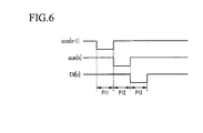
- FIG. 6 illustrates timing diagrams of a previous scan signal for inspection, a current scan signal, and a light emission control signal according to an exemplary embodiment of the present invention.
- the pixel circuit includes first to sixth transistors T11 to T16, an organic light emitting diode (OLED) element, and a capacitor C.
- the scan driver 100 generates a light emission control signal EM[n].
- the second transistor T12 is turned on in response to the current scan signal scan[n], and if the second transistor T12 is turned on, a data voltage VDATA is output to a first electrode of the first transistor T11.
- the first transistor T11 is a driving transistor, and a gate electrode of the first transistor T11 is connected to one end of the capacitor C.
- a source electrode of the first transistor T11 is connected to a drain electrode of the third transistor T13.
- the third transistor T13 is turned on in response to the scan signal scan[n]. After being turned on, the third transistor T13 diode-connects the first transistor T11.
- the fourth transistor T14 ise turned on in response to the previous scan signal scan[n-1]. After being turned on, an initial voltage VINIT is applied to one end of the capacitor C through the fourth transistor T14.
- the fifth transistor T15 and the sixth transistor T16 are turned on in response to a light emission control signal EM[n]. After being turned on, the power voltage ELVDD are supplied to the second electrode of the first transistor T11 through the fifth transistor T15. If the sixth transistor T16 is turned on, the drain current of the first transistor T11 is supplied to the OLED. The OLED may emit light corresponding to the drain current of the first transistor T11.
- the previous scan signal scan[n-1] has a low level.
- the fourth transistor T14 is turned on, thereby supplying an initial voltage to one end of the capacitor C.
- the current scan signal S[n] has a low level.
- the third transistor T13 is turned on, thereby diode-connecting the first transistor T11 and supplying a data voltage VDATA[n] to the second electrode of the first transistor T11 through the second transistor T12. Then, the voltage at the gate electrode of the first transistor T11, the first electrode, and one end of the capacitor C becomes a voltage VDATA + VTH.
- the light emission control signal EM[n] has a low level, thereby turning on the fifth transistor T15 and the sixth transistor T16.
- the power voltage ELVDD is supplied to the first electrode of the first transistor T11, a current is generated corresponding to the voltage difference VGS of the first electrode and the gate electrode of the first transistor T11 as in Equation 1.
- the voltage of the gate is VDATA + VTH, and the first electrode becomes a source electrode. Therefore, a voltage VGS becomes a voltage VDATA+VTH-ELVDD.
- a voltage VDATA is a data voltage VDATA[n]
- a voltage VTH is a threshold voltage of the first transistor T11. Then, a current is generated as in Equation 2.
- the power voltage ELVDD is the first power voltage VVDD or a voltage corresponding to the first power voltage VVDD.
- I OLED ⁇ 2 ( VGS - VTH ⁇ ) 2
- I OLED ⁇ 2 ( ELVDD - VDATA ⁇ ) 2
- Equations 1 and 2 ⁇ is a constant that is determined depending on the characteristics of the first transistor T11.
- the OLED display of a target cell for inspection in a sheet generates a current corresponding to the data voltage so that the organic light emitting element emits light, and the OLED display of a non-target cell for inspection does not emit light. Therefore, interference between adjacent cells may be prevented, and the voltage drop may be prevented because the power voltage ELVDD is not supplied to the driving transistor of the non-selected cell.
Landscapes
- Engineering & Computer Science (AREA)
- Physics & Mathematics (AREA)
- General Physics & Mathematics (AREA)
- Computer Hardware Design (AREA)
- Theoretical Computer Science (AREA)
- Control Of Indicators Other Than Cathode Ray Tubes (AREA)
- Electroluminescent Light Sources (AREA)
- Testing Electric Properties And Detecting Electric Faults (AREA)
- Control Of El Displays (AREA)
Abstract
Description
- The present invention relates to an organic light emitting diode (OLED) display, an inspection circuit of an OLED display, and a driving method thereof.
- With the development of the electronics industry and the increase in the amount of information, there has been much research in active progress for developing a large screen display. Flat panel displays providing a large screen and low power consumption have been introduced to address these issues. Examples thereof include a liquid crystal display (LCD), a plasma display panel (PDP), and an organic light emitting diode (OLED) display. Particularly, OLED displays have been receiving attention as a flat panel display that can be made extremely thin, lightweight and as having superior color reproducibility. An OLED display may have various additional advantages, e.g., a faster response speed than an LCD, superior luminance due to its self emission, a simple structure, and an easy manufacturing process. Therefore, an OLED display can be used for various products, e.g., a backlight, a portable terminal, a GPS system, a,laptop computer, and a large screen TV.
- Generally, in an OLED display, a first line extending in a first direction for receiving a scan signal and a light emission control signal may be disposed around an organic light emitting diode, a second line extending in a second direction for applying a data signal may be disposed to cross the first line, and a pixel may be disposed at an intersection between the first and second lines. Since such an OLED display may be manufactured through a plurality of manufacturing processes, the manufacturing cost thereof may increase and the reliability may be degraded according to defects caused during the manufacturing processes.
- A conventional method of inspecting a sheet having a plurality of cells may generate a defect at a scan line as a result of interference between adjacent cells, and may induce malfunctions of turning on/off adjacent cells because of a voltage drop caused by leakage current. However, this method cannot measure the power consumption of a scan driver in a sheet unit before scribing.
- The above information disclosed in this Background section is only for enhancement of understanding of the background of the invention and therefore it may contain information that does not form the prior art that is already known in this country to a person of ordinary skill in the art.
- The present invention is therefore directed to an organic light emitting diode (OLED) display and a driving method of an inspection circuit of an OLED display, which substantially overcome one or more of the problems due to the limitations and disadvantages of the related art.
- It is therefore an object of the present invention to provide an OLED display and a driving method of an inspection circuit of an OLED display for reducing or preventing interference between cells.
- Another object of the present invention to provide an OLED display and a driving method of an inspection circuit of an OLED display for preventing or reducing a voltage drop generated during a sheet inspection.
- Yet another object of the present invention is to provide an OLED display and a driving method of an inspection circuit of an OLED display for measuring the power consumption of a scan driver.
- Accordingly, a first aspect of the present invention provides an organic light emitting diode (OLED) display, as set out in
Claim 1. Preferred features are set out inClaims 2 to 11. - A second aspect of the present invention provides a driving method of an inspection circuit in an organic light emitting diode (OLED) display as set out in Claim 12. Preferred features are set out in Claims 13 to 20.
- The above and other features and advantages of the present invention will become more apparent to those of ordinary skill in the art by describing in detail embodiments thereof with reference to the attached drawings, in which:
- FIG. 1 illustrates a schematic plan view of an organic light emitting diode (OLED) display according to an embodiment of the present invention;
- FIG. 2 illustrates a schematic diagram of a first signal input section according to an embodiment of the present invention;
- FIG. 3 illustrates a schematic diagram of a second signal input section according to an embodiment of the present invention;
- FIG. 4 illustrates a schematic diagram of a signal receiving unit according to an embodiment of the present invention;
- FIG. 5 illustrates a schematic diagram of a pixel circuit according to an embodiment of the present invention; and
- FIG. 6 illustrates a timing diagram of a previous scan signal for inspection, a current scan signal, and a light emission control signal according to an exemplary embodiment of the present invention.
- As will be described in detail below, an organic light emitting diode (OLED) display and a method for driving an inspection circuit of the OLED display according to embodiments of the present invention are provided, which may reduce or prevent interference between cells and/or a voltage drop while inspecting a sheet including the OLED display.
- In the following detailed description, only certain embodiments of the present invention have been shown and described, simply by way of illustration. As those skilled in the art would realize, the described embodiments may be modified in various different ways, all without departing from the scope of the present invention. In order to clearly describe the present invention, parts of the drawings unrelated to the description of the present invention have been omitted. Like reference numerals designate like elements throughout the specification.
- When a first part is referred to as being "connected" to a second part, it could mean that the first part is directly connected to the second part, and it could also mean that the first part and the second part are "electrically connected" having a third element between them. Furthermore, when a part is referred to as "including" a constituent element, it does not mean that the part excludes other constituent elements, but it means that the part can further include other constituent elements, unless otherwise specified.
- FIG. 1 illustrates a schematic plan view of a cell of a circuit that is a subject of an inspecting method according to an embodiment of the present invention.
- As shown in FIG. 1, a
cell 1000 of an original circuit includes ascan driver 100, adata driver 200, adisplay unit 300, and aninspection circuit 400 of an OLED display. Thecell 1000 is connected to a first power supply line supplying a power voltage VVDD, a second power supply line supplying a power voltage VVSS, first and second inspection signal supply lines that supply first and second inspection signals DS1 and DS2, a scan signal supply line that supplies an output signal OS corresponding to a scan signal scan[n], and a first control signal line SCTL and a second control signal line SCTLB that supplies a first control signal and a second control signal, respectively. - The
scan driver 100 receives a frame pulse FLM, a first shiftclock signal SFTCLK, a second shiftclock signal SFTCLKB, a first clock signal SCLK1, and a second clock signal SCLK2, and may generate a scan signal to be supplied to a respective scan line S1-Sn. - The
data driver 200 generates a data signal corresponding to an externally input image input signal, and may supply the data signal to a respective data line D1-Dm. - The
display unit 300 includes a plurality ofpixel circuits 310. Eachpixel circuit 310 includes an organic light emitting element, a switch, a capacitor, and a driving transistor. Eachpixel circuit 310 is disposed at a region where the scans line S1-Sn and the data lines D1-Dm intersect each other. Eachpixel circuit 310 is connected to respective ones of the scan lines S1-Sn and the data lines D1-Dm, and a current corresponding to the data signal input in response to a scan signal is generated. This current is supplied to the organic light emitting element, and the organic light emitting element emits light in response to the current. - The
inspection circuit 400 receives the first control signal SCTL, the second control signal SCTLB, and the first and the second inspection signals DS1 and DS2, and generates the frame pulse FLM, the first shiftclock signal SFTCLK, the second shiftclock signal SFTCLKB, the first clock signal SCLK1, and the second clock signal SCLK2 to be output to thescan driver 100. The first control signal SCTL and the second control signal SCTLB are signals having inverse phases with respect to each other. - The
inspection circuit 400 includes a firstsignal input section 410, a secondsignal input section 420, and asignal receiving unit 430. The firstsignal input section 410 generates the frame pulse FLM, the first shiftclock signal SFTCLK, and the second shiftclock signal SFTCLKB, and outputs them to thescan driver 100. The secondsignal input section 420 generates the first clock signal SCLK1 and the second clock signal SCLK2, and outputs them to thescan driver 100. Thesignal receiving unit 430 receives the scan signal output from at least one of the scan lines S1-Sn of thedisplay unit 300, and generates and outputs the output signal OS corresponding to the received scan signal scan[n]. A scan waveform may be measured using the signal output from thesignal receiving unit 430, and a power consumption level of thescan driver 100 may be measured. - Although the
inspection circuit 400 illustrates only the first signal input section and the second signal input section in FIG. 1 consistent with the embodiment of the present invention, the frame pulse FLM, the first shiftclock signal SFTCLK, the second shiftclock signal SFTCLKB, the first clock signal SCLK1, and the second clock signal SCLK2 may be generated in a separate signal input section. However, since the frame pulse FLM, the first shiftclock signal SFTCLK, and the second shiftclock signal SFTCLKB may be generated in the firstsignal input section 410 having substantially the same structure, only one firstsignal input section 410 is illustrated for better understanding and ease of description. Furthermore, since the first clock signal SCLK1 and the second clock signal SCLK2 may be generated in the second signal input section having substantially the same structure, only one secondsignal input section 420 is illustrated for better understanding and ease of description. - As shown in FIG. 1, a
inspection signal generator 500 generates the first and second inspection signals DS1 and DS2, the first power voltage VVDD, the second power voltage VVSS, and the first and second control signals SCTL and SCTLB, and supplies the same to a sheet including thecell 1000. Theinspection signal generator 500 receives the signal OS output from thecell 1000 that is subjected to the inspection. The power consumption level of thescan driver 100 is measured according to the received signal. FIG. 1 illustrates that thesignal receiving unit 430 receives the scan signal output from the scan line Sn. However, the present invention is not limited to this. Thesignal receiving unit 430 may receive two or more scan signals to measure waveforms of each scan signal, and the power consumption level of thescan driver 100 may be measured according to the measured waveforms of the scan signals. - FIG. 2 illustrates a schematic diagram of the first
signal input section 410 according to an embodiment of the present invention. - The first
signal input section 410 consistent with the embodiment of the present invention generates the frame pulse FLM, the first shiftclock signal SFTCLK, and the second shiftclock signal SFTCLKB, in accordance with the first power voltage VVDD and/or the second power voltage VVSS. - As shown in FIG. 2, the first signal input section includes a three-
phase inverter 411, afirst inverter 412, and a first transistor T1. Hereinafter, a transistor consistent with the embodiment of the present invention includes a source electrode, a drain electrode, and a gate electrode as a first electrode, a second electrode, and a control electrode, respectively. Furthermore, a complementary metal oxide semiconductor (CMOS) may be used as a complementary semiconductor. - The three-
phase inverter 411 includes two PMOS transistors P1 and P2, and two NMOS transistors N1 and N2. The two PMOS transistors P1 and P2 form a first inverter sub-circuit unit of the three-phase inverter, and the two NMOS transistor N1 and N2 form a second inverter sub-circuit unit of the three-phase inverter. Furthermore, the PMOS transistor P2 and the NMOS transistor N2 form one CMOS inverter. A node where the first inverter sub-circuit unit and the second inverter sub-circuit unit meet serves as an output terminal of the three-phase inverter 411. - The second control signal SCTLB is supplied to a gate electrode of the PMOS transistor P1, and the first control signal SCTL is supplied to a gate electrode of the NMOS transistor N1. At this time, if the first and second control signals SCTL and SCTLB have a high level and a low level, respectively, the PMOS transistor P1 and the NMOS transistor N1 are turned on. Thus, an output may be determined according to the first inspection signal DS1, which is supplied to gate electrodes of the PMOS transistor P2 and the NMOS transistor N2. If the first inspection signal DS1 has a high level, then the NMOS transistor N2 is turned on. At this time, if the first control signal SCTL has a high level, the voltage of the second power supply VVSS is output to an output terminal of the three-phase inverter. If the first inspection signal DS1 has a low level, then the PMOS transistor P2 is turned on. At this time, if the second control signal SCTLB has a low level, the first power voltage VVDD is output to an output terminal of the three-phase inverter.
- The second control signal SCTLB is supplied to a gate electrode of the first transistor T1. A drain electrode of the first transistor T1 is connected to the output terminal of the three-
phase inverter 411, and a source electrode of the first transistor T1 is connected to the second power voltage VVSS. An input terminal of thefirst inverter 412 is connected to the output terminal of the three-phase inverter 411 and the drain electrode of the first transistor T1. - An output terminal of the
first inverter 412 is connected to thescan driver 100. The first transistor T1 is turned on when an output of the three-phase inverter 411 is determined by the first and second control signals SCTL and SCTLB regardless of the input signal, and supplies the voltage of the second power voltage VVSS to thefirst inverter 412. If the first and second control signals SCTL and SCTLB have a low level and a high level, respectively, then the PMOS transistor P1 and the NMOS transistor N1 are both turned off. Thus, an output may be determined regardless of the input signal. At this time, the first transistor T1 is turned on, and supplies the second power voltage VVSS to the input terminal of thefirst inverter 412. - The
first inverter 412 includes a CMOS transistor having a PMOS transistor P3 and an NMOS transistor N3. If an input voltage is the first power voltage VVDD, then the voltage of the second power supply WSS is output. If the input voltage is the second power voltage VVSS, then the first power voltage VVDD is output. Consistent with the embodiment of the present invention, the first power voltage VVDD may be a voltage of a high level, and the second power voltage WSS may be a voltage of a low level. - FIG. 3 illustrates a schematic diagram of the second
signal input section 420 according to an embodiment of the present invention. - The second
signal input section 420 generates the first clock signal SCLK1 and the second clock signal SCLK2, and may receive the first power voltage VVDD or the second power voltage VVSS. - As shown in FIG. 3, the second signal input section includes a three-
phase inverter 421, asecond inverter 422, and a second transistor T2. - The three-
phase inverter 421 includes two PMOS transistors P4 and P5, and two NMOS transistors N4 and N5. The two PMOS transistors P4 and P5 forms a third inverter sub-circuit unit of the three-phase inverter 421, and the two NMOS transistors N4 and N5 form a fourth inverter sub-circuit unit of the three-phase inverter 421. The PMOS transistor P5 and the NMOS transistor N5 form one CMOS inverter. A node where the third inverter sub-circuit unit and the fourth inverter sub-circuit unit meet serves as an output terminal of the three-phase inverter 421. - The second control signal SCTLB is supplied to a gate electrode of the PMOS transistor P4, and the first control signal SCTL is supplied to a gate electrode of the NMOS transistor N4. At this time, if the first and second control signals SCTL and SCTLB have a high level and a low level, respectively, the PMOS transistor P4 and the NMOS transistor N4 are turned on. Thus, an output may be determined according to the second inspection signal DS2. If the second inspection signal DS2 has a high level, then the NMOS transistor N5 is turned on. At this time, if the first control signal SCTL has a high level, the voltage of the second power supply VVSS is output to an output terminal of the three-
phase inverter 421. If the second inspection signal DS2 has a low level, then the PMOS transistor P5 is turned on. At this time, if the second control signal SCTLB has a low level, the voltage of the first power supply VVDD is output to an output terminal of the three-phase inverter 421. - The first control signal SCTL is supplied to a gate electrode of the second transistor T2. A drain electrode of the second transistor T2 is connected to the output terminal of the three-
phase inverter 421, and a source electrode of the second transistor T2 is connected to the first power supply VVDD. - An input terminal of the
second inverter 422 is connected to the output terminal of the three-phase inverter 421 and the drain of the second transistor T2. An output terminal of thesecond inverter 422 is connected to thescan driver 100. The second transistor T2 is turned on when an output of the three-phase inverter 421 is determined by the first and second control signals SCTL and SCTLB regardless of the input signal, and supplies the voltage of the first power supply VVDD to thesecond inverter 422. If the first and second control signals SCTL and SCTLB are a low level and a high level, respectively, then the PMOS transistor P4 and the NMOS transistor N4 are both turned off. Thus, an output may be determined regardless of the input signal. At this time, the second transistor T2 is turned on and supplies the first power voltage VVDD to thesecond inverter 422. - If an input voltage input to the input terminal of the
second inverter 422 is the first power voltage VVDD, then thesecond inverter 422 outputs the second power voltage VVSS. If the input voltage input to the input terminal of thesecond inverter 422 is the second power voltage VVSS, then thesecond inverter 422 outputs the first power voltage VVDD. Consistent with the embodiment of the present invention, the first power voltage VVDD may be a voltage of a high level, and the second power voltage VVSS may be a voltage of a low level. - FIG. 4 illustrates a schematic diagram of a
signal receiving unit 430 according to an embodiment of the present invention. - The
signal receiving unit 430 has an input terminal connected to at least one of the scan lines S1-Sn, and receives a respective scan signal scan[n] applied to the scan line S1-Sn, generates the signal OS corresponding to the scan signal scan[n], and outputs the generated signal OS. Thesignal receiving unit 430 according to the present embodiment includes a three-phase inverter 431. - The three-
phase inverter 431 includes two PMOS transistors P6 and P7, and two NMOS transistors N6 and N7. The two PMOS transistors P6 and P7 form a fifth inverter sub-circuit unit of the three-phase inverter 431, and the two NMOS transistors N6 and N7 form a sixth inverter sub-circuit unit of the three-phase inverter 431. The PMOS transistor P7 and the NMOS transistor N7 form one CMOS inverter. A node where the fifth inverter sub-circuit unit and the sixth inverter sub-circuit unit meet serves as an output terminal. - As shown in FIG. 4, the three-
phase inverter 431 may output a first power voltage VVDD or a second power voltage VVSS corresponding to a scan signal scan[n] when the first control signal SCTL and the second control signal SCTLB are a high level and a low level, respectively. The scan signal scan[n] is supplied to gate electrodes of the PMOS transistor P7 and the NMOS transistor N7. - If the scan signal scan[n] has a low level, the PMOS transistor P7 is turned on. If the second control signal SCTLB has a low level when the PMOS transistor P7 is turned on, the first power voltage VVDD is supplied to the output node. Then, the signal OS output from the
signal receiving unit 430 becomes the first power voltage VVDD, and is supplied to the inspectionpower voltage generator 500. At this time, based on the result, a low level scan signal may be applied, and it may be determined that the OLED display operates normally. - On the other hand, if the scan signal is a high level and the first control signal SCTL is a high level, NMOS transistors N6 and N7 are turned on, and the signal OS output from the
signal receiving unit 430 becomes the second power voltage VVSS, and is output to theinspection signal generator 500. Then, a high level scan signal is applied, and it can be determined that the scan signal is output from thescan driver 100 normally. - A waveform of a scan signal may be estimated by measuring a signal waveform output from the
signal receiving unit 430, and the power consumption of a scan driver may be measured using the estimated waveform. - According to the embodiment of the present invention, an OLED display having a target cell for inspection operates normally in a sheet.
- When the OLED display of other cells except the target cell do not operate normally, a pixel circuit of each OLED display does not bias in the sheet. Accordingly, a black image may be displayed. In order for an OLED display to not operate normally, signals input to the scan driver, e.g., the frame pulse FLM, the first shiftclock signal SFTCLK, the second shiftclock signal SFTCLKB, the first clock signal CLK1, and the second clock signal SCLK2, may satisfy following conditions. The frame pulse FLM, the first shiftclock signal SFTCLK, and the second shiftclock signal sre the first power voltage VVDD, and the first clock signal CLK1 and the second clock signal SCLK2 is the second power voltage WSS.
- The
inspection circuit 400 generates the frame pulse FLM, the first shiftclock signal SFTCLK, the second shiftclock signal SFTCLKB, the first clock signal CLK1, and the second clock signal SCLK2 according to an inspection signal DS if the first control signal SCTL and the second control signal SCTLB are a high level and a low level, respectively. Then, theinspection circuit 400 outputs the generated signals to thescan driver 100. - On the contrary, if the first control signal SCTL and the second control signal SCTLB are a low level and a high level, respectively, the
inspection circuit 400 generates the frame pulse FLM, the first shiftclock signal SFTCLK, and the second shiftclock signal SFTCLKB as the first power voltage VVDD, and generates the first clock signal CLK1 and the second clock signal SCLK2 as the second power voltage VVDD, regardless of the inspection signal DS. Then, theinspection circuit 400 outputs the generated signal to thescan driver 100. - As described above, the OLED display according to an embodiment of the present invention may inspect desired cells from an original circuit unit without scribing.
- Also, if each
cell 1000 is cut off from the sheet, theinspection circuit 400 may remain at eachcell 1000. That is, theinspection circuit 400 according to an embodiment of the present invention may be placed at a trimming margin where thecell 1000 is trimmed from the sheet. After cutting off thecell 1000, theinspection circuit 400 may remain at a substrate where the OLED display is formed. However, thescan driver 100 and thedata driver 200 may be connected to a signal controller (not shown) when the OLED display is completely manufactured after inspection. The signal controller receives a vertical synchronization signal, a horizontal synchronization signal, a clock signal, and external image data, generates a scan signal and a data signal, and outputs them to a scan driver and a data driver. - Hereinafter, in a
cell 1000 having an OLED display according to an embodiment of the present invention that is a target for inspection, the operation of a pixel circuit will be described with reference to FIG. 5 and FIG. 6. - FIG. 5 illustrates a schematic diagram of a pixel circuit according to an embodiment of the present invention. FIG. 6 illustrates timing diagrams of a previous scan signal for inspection, a current scan signal, and a light emission control signal according to an exemplary embodiment of the present invention.
- As shown in FIG. 5, the pixel circuit includes first to sixth transistors T11 to T16, an organic light emitting diode (OLED) element, and a capacitor C. In the pixel circuit according to an embodiment of the present invention, the
scan driver 100 generates a light emission control signal EM[n]. - The second transistor T12 is turned on in response to the current scan signal scan[n], and if the second transistor T12 is turned on, a data voltage VDATA is output to a first electrode of the first transistor T11. The first transistor T11 is a driving transistor, and a gate electrode of the first transistor T11 is connected to one end of the capacitor C. A source electrode of the first transistor T11 is connected to a drain electrode of the third transistor T13. The third transistor T13 is turned on in response to the scan signal scan[n]. After being turned on, the third transistor T13 diode-connects the first transistor T11. The fourth transistor T14 ise turned on in response to the previous scan signal scan[n-1]. After being turned on, an initial voltage VINIT is applied to one end of the capacitor C through the fourth transistor T14. The fifth transistor T15 and the sixth transistor T16 are turned on in response to a light emission control signal EM[n]. After being turned on, the power voltage ELVDD are supplied to the second electrode of the first transistor T11 through the fifth transistor T15. If the sixth transistor T16 is turned on, the drain current of the first transistor T11 is supplied to the OLED. The OLED may emit light corresponding to the drain current of the first transistor T11.
- As can be seen in FIG. 6, at first, during a period P11, the previous scan signal scan[n-1] has a low level. Thus, the fourth transistor T14 is turned on, thereby supplying an initial voltage to one end of the capacitor C. During a period P12, the current scan signal S[n] has a low level. Thus, the third transistor T13 is turned on, thereby diode-connecting the first transistor T11 and supplying a data voltage VDATA[n] to the second electrode of the first transistor T11 through the second transistor T12. Then, the voltage at the gate electrode of the first transistor T11, the first electrode, and one end of the capacitor C becomes a voltage VDATA + VTH.
- During a period P13, the light emission control signal EM[n] has a low level, thereby turning on the fifth transistor T15 and the sixth transistor T16. If the power voltage ELVDD is supplied to the first electrode of the first transistor T11, a current is generated corresponding to the voltage difference VGS of the first electrode and the gate electrode of the first transistor T11 as in
Equation 1. The voltage of the gate is VDATA + VTH, and the first electrode becomes a source electrode. Therefore, a voltage VGS becomes a voltage VDATA+VTH-ELVDD. A voltage VDATA is a data voltage VDATA[n], and a voltage VTH is a threshold voltage of the first transistor T11. Then, a current is generated as inEquation 2. That is, a current is generated corresponding to a voltage compensated with the threshold voltage of the first transistor T11. Also, the power voltage ELVDD according to the present embodiment is the first power voltage VVDD or a voltage corresponding to the first power voltage VVDD.

- In
Equations - As described above, the OLED display of a target cell for inspection in a sheet generates a current corresponding to the data voltage so that the organic light emitting element emits light, and the OLED display of a non-target cell for inspection does not emit light. Therefore, interference between adjacent cells may be prevented, and the voltage drop may be prevented because the power voltage ELVDD is not supplied to the driving transistor of the non-selected cell.
- Embodiments of the present invention have been disclosed herein, and although specific terms are employed, they are used and are to be interpreted in a generic and descriptive sense only and not for purpose of limitation. Accordingly, it will be understood by those of ordinary skill in the art that various changes in form and details may be made without departing from the scope of the present invention as set forth in the following claims.
Claims (22)
- An organic light emitting diode (OLED) display, comprising:a data driver for applying a data signal;a scan driver for applying a scan signal;a driving transistor for generating a current corresponding to a voltage supplied from a first electrode and a control electrode;a switching transistor for applying the data signal to the driving transistor;an OLED electrically connected to the driving transistor; andan inspection circuit for inspecting the scan signal including a three-phase inverter circuit having an input terminal and an output terminal, wherein the input terminal is arranged to supply a first power voltage to the output terminal when an output signal is determined regardless of a signal input to the input terminal.
- An OLED display as claimed in claim 1, wherein the inspection circuit and the OLED are arranged on a same substrate.
- An OLED display as claimed in claim 2, wherein the three-phase inverter circuit is formed at a predetermined area on the same substrate as the scan driver and the data driver except areas where the scan driver and the data driver are formed.
- An OLED display as claimed in any preceding claim, wherein the three-phase inverter circuit comprises a complementary semiconductor.
- An OLED display as claimed in claim 4, wherein the three-phase inverter further comprises:a first transistor for supplying a first power voltage to a first electrode of the complementary semiconductor in response to a first signal input to a control electrode; anda second transistor for supplying the second power voltage to a second electrode of the complementary semiconductor in response to a second signal input to the control electrode.
- An OLED display as claimed in claim 5, wherein the complementary semiconductor comprises:a third transistor for supplying the first power voltage to the output terminal in response to the first signal; anda fourth transistor for supplying the second power voltage to the output terminal in response to the second signal.
- An OLED display as claimed in claim 6, wherein the first and third transistors are P channel transistors, and the second and fourth transistors are N channel transistors.
- An OLED display as claimed in any preceding claim, wherein the three-phase inverter circuit comprises a first node where a first inverter sub-circuit and a second inverter sub-circuit are connected in series, and the first node is an output terminal of the three-phase inverter circuit.
- An OLED display as claimed in claim 8, wherein the first inverter sub-circuit includes a p-type metal oxide semiconductor (PMOS), and the second inverter sub-circuit includes an n-type metal oxide semiconductor (NMOS).
- An OLED display as claimed in any preceding claim 1, wherein the inspection circuit further comprises a two-phase inverter circuit, and an input terminal of the two-phase inverter circuit is electrically connected to an output terminal of the three-phase inverter circuit.
- An OLED display as claimed in any preceding claim, wherein the three-phase inverter circuit is arranged to output a signal to be inspected.
- A driving method of an inspection circuit in an organic light emitting diode (OLED) display including an OLED, a switching transistor, a scan driver, and an inspection circuit, the driving method comprising:supplying a first control signal, a second control signal, and an inspection signal to the inspection circuit; andsupplying at least one signal corresponding to the inspection signal to the scan driver in response to the first control signal and the second control signal.
- A method as claimed in claim 12, further comprising at the scan driver, generating a scan signal for inspection using at least one signal, and applying the inspection scan signal to a control electrode of the switching transistor.
- A method as claimed in claim 13, further comprising receiving the inspection scan signal in response to the first control signal and the second control signal, reversing the received scan signal, and outputting the reversed scan signal.
- A method as claimed in claim 14, wherein the inspection scan signal is received when the first control signal and the second control signal are a high level and a low level, respectively, and the received scan signal is reversed and output.
- A method as claimed in any one of claims 13 to 15, further comprising applying the inspection scan signal to the switching transistor when the first control signal and the second control signal are a high level and a low level.
- A method as claimed in any one of claims 13 to 16, further comprising blocking the inspection scan signal when the first control signal and the second control signal are a low level and a high level, respectively.
- A method as claimed in any one of claims 12 to 17 wherein the inspection signal is supplied from an inspection signal generator.
- A method as claimed in any one of claims 12 to 18 wherein;
supplying at least one signal corresponding to the inspection signal to the scan driver comprises generating the at least one signal in response to the control signal and the inverse-phase control signal. - A method as claimed in claim 12 or 19, wherein the inspection circuit is an inspection circuit and the OLED dislay includes a power voltage line for applying a power voltage for the inspection circuit, the method further comprising
generating a scan signal using the at least one signal; and
applying the inspection power voltage to the first electrode of the switching transistor in response to the scan signal. - A method as claimed in claim 20, further comprising applying the inspection power voltage to the first electrode of the driving transistor when the control signal and the inverse-phase control signal are a high level and a low level, respectively.
- The method as claimed in claim 20 or 21, further comprising blocking the inspection power voltage from the first electrode of the driving transistor when the control signal and the inverse-phase control signal are a low level and a high level, respectively.
Applications Claiming Priority (1)
| Application Number | Priority Date | Filing Date | Title |
|---|---|---|---|
| KR1020060075175A KR100749423B1 (en) | 2006-08-09 | 2006-08-09 | Inspection circuit driving method of organic light emitting display and organic light emitting display |
Publications (3)
| Publication Number | Publication Date |
|---|---|
| EP1887728A2 true EP1887728A2 (en) | 2008-02-13 |
| EP1887728A3 EP1887728A3 (en) | 2011-01-12 |
| EP1887728B1 EP1887728B1 (en) | 2017-05-17 |
Family
ID=38602927
Family Applications (1)
| Application Number | Title | Priority Date | Filing Date |
|---|---|---|---|
| EP07252772.4A Active EP1887728B1 (en) | 2006-08-09 | 2007-07-11 | Organic light emitting display and driving method of inspection circuit of organic light emitting display |
Country Status (5)
| Country | Link |
|---|---|
| US (1) | US8054257B2 (en) |
| EP (1) | EP1887728B1 (en) |
| JP (1) | JP2008040450A (en) |
| KR (1) | KR100749423B1 (en) |
| CN (1) | CN101123069B (en) |
Families Citing this family (15)
| Publication number | Priority date | Publication date | Assignee | Title |
|---|---|---|---|---|
| KR100884463B1 (en) * | 2007-07-31 | 2009-02-20 | 삼성모바일디스플레이주식회사 | Light emitting display device and method of manufacturing the same |
| KR100958643B1 (en) * | 2008-10-17 | 2010-05-20 | 삼성모바일디스플레이주식회사 | Touch screen display device and driving method thereof |
| JP5433309B2 (en) | 2009-06-03 | 2014-03-05 | 株式会社ジャパンディスプレイ | Display device |
| US8674964B2 (en) * | 2009-07-02 | 2014-03-18 | Au Optronics Corp. | Organic light emitting diode touch display |
| KR102639239B1 (en) | 2011-05-13 | 2024-02-20 | 가부시키가이샤 한도오따이 에네루기 켄큐쇼 | Display device |
| KR101881853B1 (en) * | 2012-02-29 | 2018-07-26 | 삼성디스플레이 주식회사 | Emission driving unit, emission driver and organic light emitting display device having the same |
| CN104616611A (en) * | 2015-02-15 | 2015-05-13 | 合肥鑫晟光电科技有限公司 | Lighting detection equipment and lighting detection method |
| KR102312291B1 (en) * | 2015-02-24 | 2021-10-15 | 삼성디스플레이 주식회사 | Display device and inspecting method thereof |
| CN106504703B (en) * | 2016-10-18 | 2019-05-31 | 深圳市华星光电技术有限公司 | AMOLED pixel-driving circuit and driving method |
| JP2018132744A (en) * | 2017-02-17 | 2018-08-23 | パナソニック液晶ディスプレイ株式会社 | Display device |
| CN109427301B (en) | 2018-05-09 | 2021-01-22 | 京东方科技集团股份有限公司 | Pixel circuit, electroluminescent display panel, driving method thereof and display device |
| US11341878B2 (en) * | 2019-03-21 | 2022-05-24 | Samsung Display Co., Ltd. | Display panel and method of testing display panel |
| CN110349536B (en) * | 2019-04-08 | 2021-02-23 | 深圳市华星光电半导体显示技术有限公司 | GOA circuit and display panel |
| WO2023221042A1 (en) | 2022-05-19 | 2023-11-23 | 京东方科技集团股份有限公司 | Driving module, display panel and display apparatus |
| WO2024129081A1 (en) | 2022-12-15 | 2024-06-20 | Google Llc | Display device with variable power consumption |
Family Cites Families (17)
| Publication number | Priority date | Publication date | Assignee | Title |
|---|---|---|---|---|
| US6437596B1 (en) | 1999-01-28 | 2002-08-20 | International Business Machines Corporation | Integrated circuits for testing a display array |
| JP5051942B2 (en) | 2000-02-01 | 2012-10-17 | 株式会社半導体エネルギー研究所 | Semiconductor device |
| JP4659180B2 (en) | 2000-07-12 | 2011-03-30 | シャープ株式会社 | Display device |
| KR100906964B1 (en) * | 2002-09-25 | 2009-07-08 | 삼성전자주식회사 | Organic electroluminescent drive device and organic electroluminescent display panel having same |
| JP4211368B2 (en) | 2002-11-25 | 2009-01-21 | 沖電気工業株式会社 | Test method for display drive circuit |
| AU2003289260A1 (en) * | 2002-12-26 | 2004-07-29 | Semiconductor Energy Laboratory Co., Ltd. | Semiconductor device, method for driving semiconductor device, and method for testing semiconductor device |
| KR100964620B1 (en) | 2003-07-14 | 2010-06-22 | 삼성전자주식회사 | Manufacturing method of mother substrate for lower substrate, substrate for display panel and display panel |
| KR100566814B1 (en) | 2003-07-24 | 2006-04-03 | 엘지.필립스 엘시디 주식회사 | Shift register |
| KR100930494B1 (en) * | 2003-08-11 | 2009-12-09 | 삼성전자주식회사 | Inspection device |
| KR100951357B1 (en) | 2003-08-19 | 2010-04-08 | 삼성전자주식회사 | Liquid crystal display |
| TWI254799B (en) | 2003-12-03 | 2006-05-11 | Renesas Tech Corp | Semiconductor device and the method of testing the same |
| JP2005189834A (en) * | 2003-12-03 | 2005-07-14 | Renesas Technology Corp | Semiconductor device and its testing method |
| KR20050108886A (en) * | 2004-05-14 | 2005-11-17 | 삼성전자주식회사 | Mother board having array substrate for display panel |
| KR100662989B1 (en) * | 2004-08-20 | 2006-12-28 | 삼성에스디아이 주식회사 | Display device having an inspection circuit |
| JP4247631B2 (en) | 2004-09-06 | 2009-04-02 | ソニー株式会社 | Image display device |
| CN100405068C (en) | 2006-01-13 | 2008-07-23 | 友达光电股份有限公司 | Testing device and method for organic light-emitting display panel |
| KR100759688B1 (en) * | 2006-04-07 | 2007-09-17 | 삼성에스디아이 주식회사 | Organic light emitting display device and mother substrate which can be inspected by ledger and its inspection method |
-
2006
- 2006-08-09 KR KR1020060075175A patent/KR100749423B1/en active Active
- 2006-11-17 JP JP2006311632A patent/JP2008040450A/en active Pending
-
2007
- 2007-04-11 US US11/783,711 patent/US8054257B2/en active Active
- 2007-05-08 CN CN2007101024094A patent/CN101123069B/en active Active
- 2007-07-11 EP EP07252772.4A patent/EP1887728B1/en active Active
Non-Patent Citations (1)
| Title |
|---|
| None |
Also Published As
| Publication number | Publication date |
|---|---|
| EP1887728B1 (en) | 2017-05-17 |
| US20080036711A1 (en) | 2008-02-14 |
| CN101123069B (en) | 2011-06-08 |
| KR100749423B1 (en) | 2007-08-14 |
| EP1887728A3 (en) | 2011-01-12 |
| US8054257B2 (en) | 2011-11-08 |
| JP2008040450A (en) | 2008-02-21 |
| CN101123069A (en) | 2008-02-13 |
Similar Documents
| Publication | Publication Date | Title |
|---|---|---|
| EP1887728B1 (en) | Organic light emitting display and driving method of inspection circuit of organic light emitting display | |
| US10192485B2 (en) | Pixel compensation circuit and AMOLED display device | |
| US11011118B2 (en) | Pixel-driving circuit and a compensation method thereof, a display panel, and a display apparatus | |
| US9870735B2 (en) | Display device including double-gate transistors with reduced deterioration | |
| CN100538797C (en) | Pixel circuit of organic light emitting display | |
| US9734761B2 (en) | Pixel circuit, driving method for the same, and display device | |
| US20200273410A1 (en) | Oled pixel circuit and driving method thereof, and display device | |
| EP3242287B1 (en) | Pixel circuit and drive method therefor, and active matrix organic light-emitting display | |
| EP3680885A1 (en) | Display apparatus and method of driving display panel using the same | |
| US9548024B2 (en) | Pixel driving circuit, driving method thereof and display apparatus | |
| US20170229056A1 (en) | Pixel circuit, driving method and display panel | |
| EP3913615A1 (en) | Emission driver, display apparatus including the same and method of driving display apparatus | |
| EP2736036A2 (en) | Organic light emitting diode display device and method of driving the same | |
| US9514676B2 (en) | Pixel circuit and driving method thereof and display apparatus | |
| EP3843072A1 (en) | Pixel unit, array substrate and display terminal | |
| US20100328276A1 (en) | Organic electro-luminescence device and method of driving the same | |
| US9099040B2 (en) | Scan driver and organic light emitting display using the same | |
| KR20200137817A (en) | Gate driving circuit and repairing method of the same | |
| US10796640B2 (en) | Pixel circuit, display panel, display apparatus and driving method | |
| KR102332423B1 (en) | Shift Resistor and Display Device having the Same | |
| US8537151B2 (en) | Inspection method | |
| US20060125512A1 (en) | Method and apparatus for inspecting array substrate | |
| US20200273402A1 (en) | Display device and driving method thereof | |
| KR100749467B1 (en) | Inspection circuit driving method of organic light emitting display and organic light emitting display | |
| US20150091954A1 (en) | Liquid crystal display device |
Legal Events
| Date | Code | Title | Description |
|---|---|---|---|
| PUAI | Public reference made under article 153(3) epc to a published international application that has entered the european phase |
Free format text: ORIGINAL CODE: 0009012 |
|
| 17P | Request for examination filed |
Effective date: 20070720 |
|
| AK | Designated contracting states |
Kind code of ref document: A2 Designated state(s): AT BE BG CH CY CZ DE DK EE ES FI FR GB GR HU IE IS IT LI LT LU LV MC MT NL PL PT RO SE SI SK TR |
|
| AX | Request for extension of the european patent |
Extension state: AL BA HR MK YU |
|
| RIN1 | Information on inventor provided before grant (corrected) |
Inventor name: KWAK, WON-KYU,C/O SAMSUNG SDI CO. LTD. Inventor name: JEONG, JIN TAE,C/O LEGAL & IP TEAM, SAMSUNG SDI CO |
|
| RIC1 | Information provided on ipc code assigned before grant |
Ipc: G09G 3/32 20060101AFI20080704BHEP |
|
| RAP1 | Party data changed (applicant data changed or rights of an application transferred) |
Owner name: SAMSUNG MOBILE DISPLAY CO., LTD. |
|
| PUAL | Search report despatched |
Free format text: ORIGINAL CODE: 0009013 |
|
| AK | Designated contracting states |
Kind code of ref document: A3 Designated state(s): AT BE BG CH CY CZ DE DK EE ES FI FR GB GR HU IE IS IT LI LT LU LV MC MT NL PL PT RO SE SI SK TR |
|
| AX | Request for extension of the european patent |
Extension state: AL BA HR MK RS |
|
| AKX | Designation fees paid |
Designated state(s): DE FR GB HU PL |
|
| RAP1 | Party data changed (applicant data changed or rights of an application transferred) |
Owner name: SAMSUNG DISPLAY CO., LTD. |
|
| 17Q | First examination report despatched |
Effective date: 20150519 |
|
| RAP1 | Party data changed (applicant data changed or rights of an application transferred) |
Owner name: SAMSUNG DISPLAY CO., LTD. |
|
| REG | Reference to a national code |
Ref country code: DE Ref legal event code: R079 Ref document number: 602007051013 Country of ref document: DE Free format text: PREVIOUS MAIN CLASS: H04L0005000000 Ipc: G09G0003000000 |
|
| RIC1 | Information provided on ipc code assigned before grant |
Ipc: G09G 3/3233 20160101ALI20160531BHEP Ipc: G09G 3/00 20060101AFI20160531BHEP |
|
| GRAJ | Information related to disapproval of communication of intention to grant by the applicant or resumption of examination proceedings by the epo deleted |
Free format text: ORIGINAL CODE: EPIDOSDIGR1 |
|
| GRAP | Despatch of communication of intention to grant a patent |
Free format text: ORIGINAL CODE: EPIDOSNIGR1 |
|
| GRAP | Despatch of communication of intention to grant a patent |
Free format text: ORIGINAL CODE: EPIDOSNIGR1 |
|
| INTG | Intention to grant announced |
Effective date: 20161206 |
|
| GRAS | Grant fee paid |
Free format text: ORIGINAL CODE: EPIDOSNIGR3 |
|
| GRAA | (expected) grant |
Free format text: ORIGINAL CODE: 0009210 |
|
| AK | Designated contracting states |
Kind code of ref document: B1 Designated state(s): DE FR GB HU PL |
|
| REG | Reference to a national code |
Ref country code: GB Ref legal event code: FG4D |
|
| REG | Reference to a national code |
Ref country code: DE Ref legal event code: R096 Ref document number: 602007051013 Country of ref document: DE |
|
| PG25 | Lapsed in a contracting state [announced via postgrant information from national office to epo] |
Ref country code: PL Free format text: LAPSE BECAUSE OF FAILURE TO SUBMIT A TRANSLATION OF THE DESCRIPTION OR TO PAY THE FEE WITHIN THE PRESCRIBED TIME-LIMIT Effective date: 20170517 |
|
| REG | Reference to a national code |
Ref country code: DE Ref legal event code: R097 Ref document number: 602007051013 Country of ref document: DE |
|
| PLBE | No opposition filed within time limit |
Free format text: ORIGINAL CODE: 0009261 |
|
| STAA | Information on the status of an ep patent application or granted ep patent |
Free format text: STATUS: NO OPPOSITION FILED WITHIN TIME LIMIT |
|
| 26N | No opposition filed |
Effective date: 20180220 |
|
| GBPC | Gb: european patent ceased through non-payment of renewal fee |
Effective date: 20170817 |
|
| REG | Reference to a national code |
Ref country code: FR Ref legal event code: ST Effective date: 20180330 |
|
| PG25 | Lapsed in a contracting state [announced via postgrant information from national office to epo] |
Ref country code: FR Free format text: LAPSE BECAUSE OF NON-PAYMENT OF DUE FEES Effective date: 20170731 |
|
| PG25 | Lapsed in a contracting state [announced via postgrant information from national office to epo] |
Ref country code: GB Free format text: LAPSE BECAUSE OF NON-PAYMENT OF DUE FEES Effective date: 20170817 |
|
| PG25 | Lapsed in a contracting state [announced via postgrant information from national office to epo] |
Ref country code: HU Free format text: LAPSE BECAUSE OF FAILURE TO SUBMIT A TRANSLATION OF THE DESCRIPTION OR TO PAY THE FEE WITHIN THE PRESCRIBED TIME-LIMIT; INVALID AB INITIO Effective date: 20070711 |
|
| P01 | Opt-out of the competence of the unified patent court (upc) registered |
Effective date: 20230515 |
|
| PGFP | Annual fee paid to national office [announced via postgrant information from national office to epo] |
Ref country code: DE Payment date: 20250624 Year of fee payment: 19 |