EP1887625A2 - Pixel having intrinsic semiconductor as electrode and electroluminescent displays employing such a pixel - Google Patents
Pixel having intrinsic semiconductor as electrode and electroluminescent displays employing such a pixel Download PDFInfo
- Publication number
- EP1887625A2 EP1887625A2 EP07252804A EP07252804A EP1887625A2 EP 1887625 A2 EP1887625 A2 EP 1887625A2 EP 07252804 A EP07252804 A EP 07252804A EP 07252804 A EP07252804 A EP 07252804A EP 1887625 A2 EP1887625 A2 EP 1887625A2
- Authority
- EP
- European Patent Office
- Prior art keywords
- transistor
- electrode
- pixel
- pixel according
- capacitive element
- Prior art date
- Legal status (The legal status is an assumption and is not a legal conclusion. Google has not performed a legal analysis and makes no representation as to the accuracy of the status listed.)
- Ceased
Links
Images


Classifications
-
- H—ELECTRICITY
- H05—ELECTRIC TECHNIQUES NOT OTHERWISE PROVIDED FOR
- H05B—ELECTRIC HEATING; ELECTRIC LIGHT SOURCES NOT OTHERWISE PROVIDED FOR; CIRCUIT ARRANGEMENTS FOR ELECTRIC LIGHT SOURCES, IN GENERAL
- H05B33/00—Electroluminescent light sources
- H05B33/10—Apparatus or processes specially adapted to the manufacture of electroluminescent light sources
-
- H—ELECTRICITY
- H10—SEMICONDUCTOR DEVICES; ELECTRIC SOLID-STATE DEVICES NOT OTHERWISE PROVIDED FOR
- H10D—INORGANIC ELECTRIC SEMICONDUCTOR DEVICES
- H10D86/00—Integrated devices formed in or on insulating or conducting substrates, e.g. formed in silicon-on-insulator [SOI] substrates or on stainless steel or glass substrates
- H10D86/01—Manufacture or treatment
- H10D86/021—Manufacture or treatment of multiple TFTs
- H10D86/0251—Manufacture or treatment of multiple TFTs characterised by increasing the uniformity of device parameters
-
- H—ELECTRICITY
- H05—ELECTRIC TECHNIQUES NOT OTHERWISE PROVIDED FOR
- H05B—ELECTRIC HEATING; ELECTRIC LIGHT SOURCES NOT OTHERWISE PROVIDED FOR; CIRCUIT ARRANGEMENTS FOR ELECTRIC LIGHT SOURCES, IN GENERAL
- H05B33/00—Electroluminescent light sources
- H05B33/12—Light sources with substantially two-dimensional [2D] radiating surfaces
- H05B33/26—Light sources with substantially two-dimensional [2D] radiating surfaces characterised by the composition or arrangement of the conductive material used as an electrode
-
- H—ELECTRICITY
- H10—SEMICONDUCTOR DEVICES; ELECTRIC SOLID-STATE DEVICES NOT OTHERWISE PROVIDED FOR
- H10D—INORGANIC ELECTRIC SEMICONDUCTOR DEVICES
- H10D86/00—Integrated devices formed in or on insulating or conducting substrates, e.g. formed in silicon-on-insulator [SOI] substrates or on stainless steel or glass substrates
- H10D86/01—Manufacture or treatment
- H10D86/021—Manufacture or treatment of multiple TFTs
- H10D86/0221—Manufacture or treatment of multiple TFTs comprising manufacture, treatment or patterning of TFT semiconductor bodies
- H10D86/0223—Manufacture or treatment of multiple TFTs comprising manufacture, treatment or patterning of TFT semiconductor bodies comprising crystallisation of amorphous, microcrystalline or polycrystalline semiconductor materials
- H10D86/0225—Manufacture or treatment of multiple TFTs comprising manufacture, treatment or patterning of TFT semiconductor bodies comprising crystallisation of amorphous, microcrystalline or polycrystalline semiconductor materials using crystallisation-promoting species, e.g. using a Ni catalyst
-
- H—ELECTRICITY
- H10—SEMICONDUCTOR DEVICES; ELECTRIC SOLID-STATE DEVICES NOT OTHERWISE PROVIDED FOR
- H10D—INORGANIC ELECTRIC SEMICONDUCTOR DEVICES
- H10D86/00—Integrated devices formed in or on insulating or conducting substrates, e.g. formed in silicon-on-insulator [SOI] substrates or on stainless steel or glass substrates
- H10D86/40—Integrated devices formed in or on insulating or conducting substrates, e.g. formed in silicon-on-insulator [SOI] substrates or on stainless steel or glass substrates characterised by multiple TFTs
- H10D86/481—Integrated devices formed in or on insulating or conducting substrates, e.g. formed in silicon-on-insulator [SOI] substrates or on stainless steel or glass substrates characterised by multiple TFTs integrated with passive devices, e.g. auxiliary capacitors
-
- H—ELECTRICITY
- H10—SEMICONDUCTOR DEVICES; ELECTRIC SOLID-STATE DEVICES NOT OTHERWISE PROVIDED FOR
- H10D—INORGANIC ELECTRIC SEMICONDUCTOR DEVICES
- H10D86/00—Integrated devices formed in or on insulating or conducting substrates, e.g. formed in silicon-on-insulator [SOI] substrates or on stainless steel or glass substrates
- H10D86/40—Integrated devices formed in or on insulating or conducting substrates, e.g. formed in silicon-on-insulator [SOI] substrates or on stainless steel or glass substrates characterised by multiple TFTs
- H10D86/60—Integrated devices formed in or on insulating or conducting substrates, e.g. formed in silicon-on-insulator [SOI] substrates or on stainless steel or glass substrates characterised by multiple TFTs wherein the TFTs are in active matrices
Definitions
- the present invention relates to a pixel of an electroluminescent display and a capacitive element in a pixel. More particularly, the present invention relates to an organic light emitting diode (OLED) display capable of being manufactured at a reduced manufacturing cost by reducing additional doping processes and/or mask processes during formation of a pixel and a capacitive element thereof.
- OLED organic light emitting diode
- LCDs liquid crystal displays
- PDPs plasma display panels
- OLED displays have been introduced.
- Flat panel display devices using electroluminescent material e.g., organic electroluminescent material
- organic electroluminescent displays may be manufactured to be lighter, lower in volume, thinner and/or with improved color reproduce-ability, as compared to conventional displays.
- organic electroluminescent displays may provide advantages such as faster response speeds than LCDs, superior luminance due to being self emission type, relatively simple structure, relatively easy manufacturing process, relatively thin size and/or relatively low weight. Therefore, organic electro-luminescence displays can be used in various fields such as backlight devices, portable terminals, GPS systems, laptop computers, and large screen TVs.
- CMOS complementary-metal-oxide-semiconductor
- P-type and N-type impurities may be employed. Therefore, separate masks may be required for forming the N-type and the P-type impurity regions, which may thereby result in an increased number of masks, increased manufacturing cost and/or processing time.
- Pixels and capacitive elements that may be manufactured, e.g., at a reduced cost and/or using a simplified manufacturing process are desired.
- the present invention is therefore directed to a pixel and electroluminescent displays employing such a pixel, which substantially overcome one or more of the problems due to the limitations and disadvantages of the related art.
- a pixel as set out in Claim 1.
- Preferred features of this aspect are set out in Claims 2 to 19.
- an electroluminescent display set out in Claim 20. Preffered features of this aspect are set out in Claim 21.
- a capacitive element of a pixel of a display e.g., OLED display
- the pixel for the OLED display is connected to a data line DATA[m] for applying data signals, a plurality of scan lines SCAN[n-1], SCAN[n] crossing the data line DATA[m] for applying scan signals, and an emission control line EM[n]. More particularly, e.g., the pixel may be connected to a respective one of the scan lines SCAN[n] corresponding to the pixel and a previous one of the scan lines SCAN[n-1] corresponding to a previous pixel driven before the pixel currently being driven.
- the pixel includes a first transistor T1, a second transistor T2, a third transistor T3, a fourth transistor T4, a fifth transistor T5, a sixth transistor T6, a first capacitive element Cst, a second capacitive element C12.
- the pixel includes an organic light emitting diode (OLED).
- a gate electrode of the first transistor T1 may be electrically connected to a first terminal of the first capacitive element Cst and a first terminal of the second capacitive element C12, a source electrode of the first transistor T1 is electrically connected to a drain electrode of the second transistor T2 and a drain electrode of the fifth transistor T5, and a drain electrode of the first transistor T1 is electrically connected to a source electrode of the sixth transistor T6 and a drain electrode of the third transistor T3.
- a gate electrode of the second transistor T2 is electrically connected to the scan line SCAN[n], and a source electrode of the second transistor T2 may be electrically connected to the gate electrode of the first transistor T1.
- a gate electrode of the third transistor T3 is connected to the scan line SCAN[n], and a source electrode of the third transistor T3 is electrically connected to the data line DATA[m].
- a source electrode of the fourth transistor T4 is connected to the first terminal of the first capacitive element Cst, a drain electrode of the fourth transistor T4 is connected to an initial voltage Vinit line, and a gate electrode of the fourth transistor T4 may be connected to the previously driven scan line SCAN[n-1].
- a gate electrode of the fifth transistor T5 is connected to the emission control line EM[n], and a source electrode of the fifth transistor T5 is connected to the first power source ELVDD voltage.
- a gate electrode of the sixth transistor T6 is electrically connected to the emission control line EM[n], and a drain electrode of the sixth transistor T6 may be electrically connected to an anode of the OLED.
- a cathode of the OLED may be connected to the second power source ELVSS.
- a second terminal of the first capacitive element Cst is connected to the initial voltage Vinit line.
- a second terminal of the second capacitive element C12 is connected to the scan line SCAN[n], the gate electrode of the second transistor T2 and the gate electrode of the third transistor T3.
- the first transistor T1 is a driving transistor for converting a voltage applied between the gate and source electrodes thereof into a current.
- the second transistor T2 is be a diode-connecting transistor for diode-connecting the first transistor T1.
- the third transistor T3 is a switching transistor for applying a data voltage applied to the data line DATA[m] to the first transistor T1 in response to a scan signal applied to the scan line SCAN[n].
- the fourth transistor T4 is a switching transistor for applying an initial voltage applied to the initial voltage Vinit line to the first capacitive element Cst.
- the fifth transistor T5 is a switching transistor for applying the first power source ELVDD voltage to the source electrode of the first transistor T1.
- the sixth transistor T6 is a switching transistor for selectively blocking a current from the first transistor T1 to the OLED in response to an emission control signal applied to the emission control line EM[n].
- the first capacitive element Cst plays a role in reducing/preventing a data voltage applied between the gate and source electrodes of the first transistor T1 from dropping.
- the second capacitive element C12 is a capacitor for storing a threshold voltage of the first transistor T1 and/or compensating for a drift according to the threshold voltage of the first transistor T1.
- FIG. 2 illustrates a schematic diagram of an exemplary first capacitive element of a pixel according to one or more embodiments of the present invention.
- one terminal of the first capacitive element Cst is an intrinsic polycrystalline semiconductor and a second terminal of the first capacitive element Cst is a gate electrode.
- one terminal of the first capacitive element Cst is an intrinsic polycrystalline semiconductor. Therefore, the first or the second terminal of the first capacitive element Cst may be an intrinsic polycrystalline semiconductor.
- the intrinsic polycrystalline semiconductor layer is made, e.g., by crystallizing amorphous semiconductor into a polysilicon layer through laser annealing, solid phase crystallization, or metal induced crystallization (MIC).
- MIC metal induced crystallization
- FIG. 3 illustrates a graph of a capacitance-voltage (C-V) curve corresponding to relationship between a frequency of an alternating voltage applied to a capacitor having an intrinsic polycrystalline semiconductor as one electrode thereof and an amount of voltage across terminals of the capacitor.
- a driving range of a pixel employing a capacitor according to one or more embodiments of the invention may be determined according to a substantially stable region of the C-V curve of the capacitor over a range of frequencies.
- curve (a) corresponds to a case in which a frequency of an alternating voltage applied to the capacitor is 100Hz
- curve (b) corresponds to a case in which the frequency is 100KHz
- a driving range of a pixel of a display e.g., an OLED display, including the first capacitive element Cst employing an intrinsic polycrystalline semiconductor layer at one terminal thereof may be about -3V to about -6V, i.e., a substantially stable region for curves (a) and (b).
- the voltage across the capacitor may range from about -3V to about -6V.
- an intrinsic polycrystalline semiconductor capacitive element can be employed in a pixel of a display, e.g., an OLED display, by setting a driving range of the pixel to a predetermined range so as to correspond to a stable capacitance region in a C-V curve of the capacitor having intrinsic polycrystalline semiconductor as one electrode thereof.
- Embodiments of the invention provide a pixel including a capacitor that has an intrinsic polycrystalline semiconductor as one electrode thereof.
- Embodiments of the invention may provide a simplified and/or lower cost process for manufacturing a pixel by including a capacitor that has an intrinsic polycrystalline semiconductor as one electrode thereof and thus, may be manufactured using a fewer number of masks and/or processing steps as compared to conventional pixels.
- the intrinsic polycrystalline semiconductor layer may be formed using, e.g., excimer laser annealing (ELA), solid phase crystallization, metal induced crystallization (MIC), metal induced lateral crystallization (MILC), and/or metal induced crystallization through a cap (MICC).
- ELA excimer laser annealing
- MIC metal induced crystallization
- MILC metal induced lateral crystallization
- MILC metal induced crystallization through a cap
- FIG. 4 illustrates a schematic diagram a method of forming an intrinsic polycrystalline semiconductor layer 20 using an ELA technique.
- the ELA technique may perform crystallization by irradiating excimer laser onto amorphous silicon 10.
- the ELA technique may be implemented using a relatively simple process and the resulting intrinsic polycrystalline semiconductor layer 20 may have good current mobility.
- FIG. 5 illustrates a schematic diagram of a method of forming the intrinsic polycrystalline semiconductor layer 20 using an SPC technique.
- the SPC technique may form the intrinsic polycrystalline semiconductor layer 20a by annealing the amorphous silicon 10 at a high temperature.
- the SPC technique may also be implemented using a relatively simple process and, as compared to the ELA technique, the resulting intrinsic polycrystalline semiconductor layer 20 made using the SPC technique may have a higher electron mobility.
- FIG. 6 illustrates a schematic diagram of a method of forming the intrinsic polycrystalline semiconductor layer 20 using an MIC technique.
- the MIC technique may perform crystallization by applying a metal catalyst 30 onto the amorphous silicon 10 through sputtering or spin coating and then annealing the amorphous silicon 10 at a relatively low temperature.
- the metal catalyst 30 may be made of, e.g., Ni, Pd, and Co, etc.
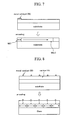
- FIG. 7 illustrates a schematic diagram of a method of forming the intrinsic polycrystalline semiconductor layer 20 using an MILC technique.
- the MILC technique may establish metal induced crystallization by depositing the metal catalyst 30 on source and drain regions, and laterally growing the crystallized seed into an activation region on the bottom of a gate.
- FIG. 8 illustrates a schematic diagram of a method of forming the intrinsic polycrystalline semiconductor layer 20 using an MICC technique.
- the MICC technique may limit the size of metal catalyst 30 infiltrating into the semiconductor layer by forming an inorganic cap layer 40 between amorphous silicon 10 and the metal catalyst 30.
- the MICC technique may reduce contamination by the metal catalyst 30 and the resulting intrinsic polycrystalline semiconductor layer 20 may be made up of grains having a substantially or completely uniform size.
- the inorganic cap layer 40 may be made of, e.g., silicon nitride (SiN x ) or silicon dioxide (SiO 2 ).
- the intrinsic polycrystalline semiconductor layer 20 formed using, e.g., any of the aforementioned crystallization techniques may have superior characteristics, as compared to amorphous silicon.
- the intrinsic polycrystalline semiconductor layer 20 may have better current mobility and/or reliability characteristics, as compared to amorphous silicon.
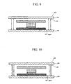
- FIG. 9 illustrates a cross-sectional diagram of an exemplary OLED display 100 including a first capacitive element employing an intrinsic polycrystalline semiconductor layer according to an embodiment of the present invention.
- One or more pixels employing an intrinsic semiconductor as an electrode of a capacitive element thereof may be disposed between the lower substrate 103 and the upper substrate 105.
- the OLED display 100 includes a sealant 101 formed between a lower substrate 103 and an upper encapsulation substrate 105 in order to prevent the deterioration of characteristics as a result of, e.g., moisture and oxygen flowing inside.
- a sealant 101 formed between a lower substrate 103 and an upper encapsulation substrate 105 in order to prevent the deterioration of characteristics as a result of, e.g., moisture and oxygen flowing inside.
- One or more pixels employing an intrinsic semiconductor as an electrode of a capacitive element thereof may be disposed between the lower substrate 103 and the upper substrate 105.
- the sealant 101 includes, e.g., a moisture absorbent material that may absorb moisture and oxygen flowing inside.
- the sealant 101 may be filled to maintain water-resistance and air-resistance on junctions or cracks, and may be made of an elastic material.
- the sealant 101 may include single component type material such as silicon-based (moisture-cure type) or acryl-based (dry-cure type) materials.
- Single component type materials may employ a mixture of a curing agent and a base polymer mixed together in advance to form a single component and packed into a container, e.g., a cartridge, in order to use instantly on the spot.
- the sealant 101 may include multiple component type materials including, e.g., modified silicon-based, polysulfide-based and/or polyurethane-based materials (reaction-cure type).
- component type materials including, e.g., modified silicon-based, polysulfide-based and/or polyurethane-based materials (reaction-cure type).
- Two component type materials may employ a curing agent and a base polymer, which are each packed in separate containers, e.g., cartridges, and then mixed together before use.
- FIG. 10 illustrates a cross-sectional diagram of another exemplary OLED display 200 including the first capacitive element employing an intrinsic polycrystalline semiconductor layer according to an embodiment of the invention.
- the OLED display 200 may be sealed with a frit 201.
- the frit 201 may include, e.g., silicon oxide (SiO 2 ), a transition metal and/or a filler having low transition temperature (CTE).
- SiO 2 silicon oxide
- CTE low transition temperature
- the frit 201 may be formed by a laser frit sealing method that locally irradiates a laser at a low temperature to seal the space between lower and upper substrates 203, 205 of the OLED display 200. Such a method may minimize the thermal damage of an organic light emitting element included in the OLED display 200, and may prevent a contaminant from flowing inside the OLED display 200 through the formed seal.
- One or more pixels employing an intrinsic semiconductor as an electrode of a capacitive element thereof may be disposed between the lower substrate 203 and the upper substrate 205.
- embodiments of the invention may provide a pixel and/or an OLED display using the same that can reduce a cost and an amount of time associated with manufacturing a pixel employable by a display, e.g., OLED display, by employing a pixel having a capacitive element that employs an intrinsic semiconductor as one electrode thereof.
- a number of masks and/or processes required for manufacturing the pixel may be reduced.
Landscapes
- Engineering & Computer Science (AREA)
- Manufacturing & Machinery (AREA)
- Electroluminescent Light Sources (AREA)
- Control Of Indicators Other Than Cathode Ray Tubes (AREA)
- Devices For Indicating Variable Information By Combining Individual Elements (AREA)
- Control Of El Displays (AREA)
- Recrystallisation Techniques (AREA)
- Thin Film Transistor (AREA)
Abstract
and a second terminal that is an intrinsic semiconductor.
Description
- The present invention relates to a pixel of an electroluminescent display and a capacitive element in a pixel. More particularly, the present invention relates to an organic light emitting diode (OLED) display capable of being manufactured at a reduced manufacturing cost by reducing additional doping processes and/or mask processes during formation of a pixel and a capacitive element thereof.
- Much progress has been made for developing large screen displays and/or flat panel displays that have large screens and/or consume relatively small amounts of power. For example, liquid crystal displays (LCDs), plasma display panels (PDPs), and OLED displays have been introduced. Flat panel display devices using electroluminescent material, e.g., organic electroluminescent material, may be manufactured to be lighter, lower in volume, thinner and/or with improved color reproduce-ability, as compared to conventional displays. More particularly, organic electroluminescent displays may provide advantages such as faster response speeds than LCDs, superior luminance due to being self emission type, relatively simple structure, relatively easy manufacturing process, relatively thin size and/or relatively low weight. Therefore, organic electro-luminescence displays can be used in various fields such as backlight devices, portable terminals, GPS systems, laptop computers, and large screen TVs.
- As progress is being made with regard to such flat panel displays, and, more particularly, electroluminescent displays, devices that may be manufactured at a lower cost and/or by an easier manufacturing process are desired. For example, conventional pixels employ complementary-metal-oxide-semiconductor (CMOS) processing and thus, employ both P-type and N-type impurities. Therefore, separate masks may be required for forming the N-type and the P-type impurity regions, which may thereby result in an increased number of masks, increased manufacturing cost and/or processing time. Pixels and capacitive elements that may be manufactured, e.g., at a reduced cost and/or using a simplified manufacturing process are desired.
- The above information disclosed in this Background section is only for enhancing understanding of the background of the invention and, therefore, may contain information that does not form prior art that is already known in this country to a person of ordinary skill in the art.
- The present invention is therefore directed to a pixel and electroluminescent displays employing such a pixel, which substantially overcome one or more of the problems due to the limitations and disadvantages of the related art.
- It is therefore a feature of an embodiment of the present invention to provide an organic light emitting diode display capable of being manufactured with a reduced number of processing steps and/or a reduced number of masks.
- According to a first aspect of the invention, there is provided a pixel as set out in
Claim 1. Preferred features of this aspect are set out in Claims 2 to 19. - According to a first aspect of the invention, there is provided an electroluminescent display set out in
Claim 20. Preffered features of this aspect are set out in Claim 21. - The above and other features and advantages of the present invention will become more apparent to those of ordinary skill in the art by describing in detail exemplary embodiments thereof with reference to the attached drawings, in which:
- FIG. 1 illustrates a circuit diagram of a pixel for an OLED display according to an embodiment of the present invention;
- FIG. 2 illustrates a schematic diagram of an exemplary first capacitive element of a pixel according to one or more embodiments of the present invention;
- FIG. 3 illustrates a graph of a relationship between a frequency of an alternating voltage applied to an exemplary capacitor employing one or more embodiments, of the invention and an amount of voltage stored in the capacitor;
- FIG. 4 illustrates a schematic diagram of a method of forming an intrinsic polycrystalline semiconductor layer using an ELA technique;
- FIG. 5 illustrates a schematic diagram of a method of forming an intrinsic polycrystalline semiconductor layer using an SPC technique;
- FIG. 6 illustrates a schematic diagram of a method of forming an intrinsic polycrystalline semiconductor layer using an MIC technique;
- FIG. 7 illustrates a schematic diagram of a method of forming an intrinsic polycrystalline semiconductor layer using an MILC technique;
- FIG. 8 illustrates a schematic diagram of a method of forming an intrinsic polycrystalline semiconductor layer using an MICC technique;
- FIG. 9 illustrates a cross-sectional diagram of an exemplary OLED display including a first capacitive element employing an intrinsic polycrystalline semiconductor layer according to an exemplary embodiment of the present invention; and
- FIG. 10 illustrates a cross-sectional diagram of another exemplary OLED display including a first capacitive element that uses an intrinsic polycrystalline semiconductor layer according to another exemplary embodiment of the present invention.
- The present invention will now be described more fully hereinafter with reference to the accompanying drawings, in which exemplary embodiments of the invention are illustrated. The invention may, however, be embodied in different forms and should not be construed as limited to the embodiments set forth herein. Rather, these embodiments are provided so that this disclosure will be thorough and complete, and will fully convey the scope of the invention to those skilled in the art.
- In the figures, the dimensions of layers and regions may be exaggerated for clarity of illustration. It will also be understood that when a layer or element is referred to as being "on" another layer or substrate, it can be directly on the other layer or substrate, or intervening elements or layers may also be present. Further, it will be understood that when a layer is referred to as being "under" another layer, it can be directly under, and one or more intervening layers may also be present. In addition, it will also be understood that when a layer is referred to as being "between" two layers, it can be the only layer between the two layers, or one or more intervening layers may also be present.
- When an element is referred to as being "connected" to a second element, it could mean that the first element is directly connected to the second element, or it could also mean that the first element and the second element are "electrically connected" having one or more elements between them. Furthermore, when an element is referred to as "including" a constituent element, unless specified otherwise, it does not mean that the element excludes any other constituent element(s), but rather means that the element may or may not include other constituent elements. Like reference numerals refer to like elements throughout the specification.
- It is an aim of the present invention to provide a pixel circuit and an OLED display using the same that can reduce the manufacturing cost and time by providing a structure having a capacitive element of a pixel of a display, e.g., OLED display, that employs an intrinsic semiconductor at one end thereof to reduce a number of masks and/or simplify the manufacturing process.
- Embodiments of the present invention will now be described with reference to the accompanying drawings.
- As shown in FIG. 1, the pixel for the OLED display according to an embodiment of the present invention is connected to a data line DATA[m] for applying data signals, a plurality of scan lines SCAN[n-1], SCAN[n] crossing the data line DATA[m] for applying scan signals, and an emission control line EM[n]. More particularly, e.g., the pixel may be connected to a respective one of the scan lines SCAN[n] corresponding to the pixel and a previous one of the scan lines SCAN[n-1] corresponding to a previous pixel driven before the pixel currently being driven. The pixel includes a first transistor T1, a second transistor T2, a third transistor T3, a fourth transistor T4, a fifth transistor T5, a sixth transistor T6, a first capacitive element Cst, a second capacitive element C12. The pixel includes an organic light emitting diode (OLED).
- A gate electrode of the first transistor T1 may be electrically connected to a first terminal of the first capacitive element Cst and a first terminal of the second capacitive element C12, a source electrode of the first transistor T1 is electrically connected to a drain electrode of the second transistor T2 and a drain electrode of the fifth transistor T5, and a drain electrode of the first transistor T1 is electrically connected to a source electrode of the sixth transistor T6 and a drain electrode of the third transistor T3. A gate electrode of the second transistor T2 is electrically connected to the scan line SCAN[n], and a source electrode of the second transistor T2 may be electrically connected to the gate electrode of the first transistor T1.
- A gate electrode of the third transistor T3 is connected to the scan line SCAN[n], and a source electrode of the third transistor T3 is electrically connected to the data line DATA[m]. A source electrode of the fourth transistor T4 is connected to the first terminal of the first capacitive element Cst, a drain electrode of the fourth transistor T4 is connected to an initial voltage Vinit line, and a gate electrode of the fourth transistor T4 may be connected to the previously driven scan line SCAN[n-1].
- A gate electrode of the fifth transistor T5 is connected to the emission control line EM[n], and a source electrode of the fifth transistor T5 is connected to the first power source ELVDD voltage. A gate electrode of the sixth transistor T6 is electrically connected to the emission control line EM[n], and a drain electrode of the sixth transistor T6 may be electrically connected to an anode of the OLED. A cathode of the OLED may be connected to the second power source ELVSS.
- A second terminal of the first capacitive element Cst is connected to the initial voltage Vinit line. A second terminal of the second capacitive element C12 is connected to the scan line SCAN[n], the gate electrode of the second transistor T2 and the gate electrode of the third transistor T3.
- The first transistor T1 is a driving transistor for converting a voltage applied between the gate and source electrodes thereof into a current. The second transistor T2 is be a diode-connecting transistor for diode-connecting the first transistor T1. The third transistor T3 is a switching transistor for applying a data voltage applied to the data line DATA[m] to the first transistor T1 in response to a scan signal applied to the scan line SCAN[n].
- The fourth transistor T4 is a switching transistor for applying an initial voltage applied to the initial voltage Vinit line to the first capacitive element Cst. The fifth transistor T5 is a switching transistor for applying the first power source ELVDD voltage to the source electrode of the first transistor T1.
- The sixth transistor T6 is a switching transistor for selectively blocking a current from the first transistor T1 to the OLED in response to an emission control signal applied to the emission control line EM[n].
- The first capacitive element Cst plays a role in reducing/preventing a data voltage applied between the gate and source electrodes of the first transistor T1 from dropping. The second capacitive element C12 is a capacitor for storing a threshold voltage of the first transistor T1 and/or compensating for a drift according to the threshold voltage of the first transistor T1.
- FIG. 2 illustrates a schematic diagram of an exemplary first capacitive element of a pixel according to one or more embodiments of the present invention. As shown in FIG. 2, in some embodiments of the invention, one terminal of the first capacitive element Cst is an intrinsic polycrystalline semiconductor and a second terminal of the first capacitive element Cst is a gate electrode. In embodiments of the invention, one terminal of the first capacitive element Cst is an intrinsic polycrystalline semiconductor. Therefore, the first or the second terminal of the first capacitive element Cst may be an intrinsic polycrystalline semiconductor.
- In some embodiments of the invention, the intrinsic polycrystalline semiconductor layer is made, e.g., by crystallizing amorphous semiconductor into a polysilicon layer through laser annealing, solid phase crystallization, or metal induced crystallization (MIC).
- FIG. 3 illustrates a graph of a capacitance-voltage (C-V) curve corresponding to relationship between a frequency of an alternating voltage applied to a capacitor having an intrinsic polycrystalline semiconductor as one electrode thereof and an amount of voltage across terminals of the capacitor. A driving range of a pixel employing a capacitor according to one or more embodiments of the invention may be determined according to a substantially stable region of the C-V curve of the capacitor over a range of frequencies.
- Referring to FIG. 3, curve (a) corresponds to a case in which a frequency of an alternating voltage applied to the capacitor is 100Hz, and curve (b) corresponds to a case in which the frequency is 100KHz. As shown in FIG. 3, a driving range of a pixel of a display, e.g., an OLED display, including the first capacitive element Cst employing an intrinsic polycrystalline semiconductor layer at one terminal thereof may be about -3V to about -6V, i.e., a substantially stable region for curves (a) and (b). In the embodiment shown in FIG. 3, when the frequency range of an alternating voltage input into the capacitor is from about 100Hz to about 100KHz, the voltage across the capacitor may range from about -3V to about -6V.
- In embodiments of the invention, an intrinsic polycrystalline semiconductor capacitive element can be employed in a pixel of a display, e.g., an OLED display, by setting a driving range of the pixel to a predetermined range so as to correspond to a stable capacitance region in a C-V curve of the capacitor having intrinsic polycrystalline semiconductor as one electrode thereof.
- Embodiments of the invention provide a pixel including a capacitor that has an intrinsic polycrystalline semiconductor as one electrode thereof. Embodiments of the invention may provide a simplified and/or lower cost process for manufacturing a pixel by including a capacitor that has an intrinsic polycrystalline semiconductor as one electrode thereof and thus, may be manufactured using a fewer number of masks and/or processing steps as compared to conventional pixels.
- An exemplary method of forming an intrinsic polycrystalline semiconductor layer will be described below.
- In some embodiments of the invention, the intrinsic polycrystalline semiconductor layer may be formed using, e.g., excimer laser annealing (ELA), solid phase crystallization, metal induced crystallization (MIC), metal induced lateral crystallization (MILC), and/or metal induced crystallization through a cap (MICC).
- FIG. 4 illustrates a schematic diagram a method of forming an intrinsic
polycrystalline semiconductor layer 20 using an ELA technique. As shown in FIG. 4, the ELA technique may perform crystallization by irradiating excimer laser ontoamorphous silicon 10. The ELA technique may be implemented using a relatively simple process and the resulting intrinsicpolycrystalline semiconductor layer 20 may have good current mobility. - FIG. 5 illustrates a schematic diagram of a method of forming the intrinsic
polycrystalline semiconductor layer 20 using an SPC technique. As shown in FIG. 5, the SPC technique may form the intrinsic polycrystalline semiconductor layer 20a by annealing theamorphous silicon 10 at a high temperature. The SPC technique may also be implemented using a relatively simple process and, as compared to the ELA technique, the resulting intrinsicpolycrystalline semiconductor layer 20 made using the SPC technique may have a higher electron mobility. - FIG. 6 illustrates a schematic diagram of a method of forming the intrinsic
polycrystalline semiconductor layer 20 using an MIC technique. As shown in FIG. 6, the MIC technique may perform crystallization by applying ametal catalyst 30 onto theamorphous silicon 10 through sputtering or spin coating and then annealing theamorphous silicon 10 at a relatively low temperature. In some embodiments of the invention, themetal catalyst 30 may be made of, e.g., Ni, Pd, and Co, etc. - FIG. 7 illustrates a schematic diagram of a method of forming the intrinsic
polycrystalline semiconductor layer 20 using an MILC technique. As shown in FIG. 7, the MILC technique may establish metal induced crystallization by depositing themetal catalyst 30 on source and drain regions, and laterally growing the crystallized seed into an activation region on the bottom of a gate. - FIG. 8 illustrates a schematic diagram of a method of forming the intrinsic
polycrystalline semiconductor layer 20 using an MICC technique. As shown in FIG. 8, the MICC technique may limit the size ofmetal catalyst 30 infiltrating into the semiconductor layer by forming aninorganic cap layer 40 betweenamorphous silicon 10 and themetal catalyst 30. The MICC technique may reduce contamination by themetal catalyst 30 and the resulting intrinsicpolycrystalline semiconductor layer 20 may be made up of grains having a substantially or completely uniform size. In some embodiments of the invention, theinorganic cap layer 40 may be made of, e.g., silicon nitride (SiNx) or silicon dioxide (SiO2). - The intrinsic
polycrystalline semiconductor layer 20 formed using, e.g., any of the aforementioned crystallization techniques may have superior characteristics, as compared to amorphous silicon. For example, the intrinsicpolycrystalline semiconductor layer 20 may have better current mobility and/or reliability characteristics, as compared to amorphous silicon. - FIG. 9 illustrates a cross-sectional diagram of an
exemplary OLED display 100 including a first capacitive element employing an intrinsic polycrystalline semiconductor layer according to an embodiment of the present invention. One or more pixels employing an intrinsic semiconductor as an electrode of a capacitive element thereof may be disposed between thelower substrate 103 and theupper substrate 105. - As shown in FIG. 9, the
OLED display 100 includes asealant 101 formed between alower substrate 103 and anupper encapsulation substrate 105 in order to prevent the deterioration of characteristics as a result of, e.g., moisture and oxygen flowing inside. One or more pixels employing an intrinsic semiconductor as an electrode of a capacitive element thereof may be disposed between thelower substrate 103 and theupper substrate 105. - The
sealant 101 includes, e.g., a moisture absorbent material that may absorb moisture and oxygen flowing inside. Thesealant 101 may be filled to maintain water-resistance and air-resistance on junctions or cracks, and may be made of an elastic material. - In some embodiments of the invention, e.g., the
sealant 101 may include single component type material such as silicon-based (moisture-cure type) or acryl-based (dry-cure type) materials. Single component type materials may employ a mixture of a curing agent and a base polymer mixed together in advance to form a single component and packed into a container, e.g., a cartridge, in order to use instantly on the spot. - In other embodiments of the invention, e.g., the
sealant 101 may include multiple component type materials including, e.g., modified silicon-based, polysulfide-based and/or polyurethane-based materials (reaction-cure type). Two component type materials may employ a curing agent and a base polymer, which are each packed in separate containers, e.g., cartridges, and then mixed together before use. - FIG. 10 illustrates a cross-sectional diagram of another
exemplary OLED display 200 including the first capacitive element employing an intrinsic polycrystalline semiconductor layer according to an embodiment of the invention. - The
OLED display 200 may be sealed with afrit 201. In some embodiments of the invention, thefrit 201 may include, e.g., silicon oxide (SiO2), a transition metal and/or a filler having low transition temperature (CTE). When the frit 201 material is irradiated, thefrit 201 may soften and may form a bond, thereby forming a seal while avoiding thermal damage to theOLED display 200. - In some embodiments of the invention, the
frit 201 may be formed by a laser frit sealing method that locally irradiates a laser at a low temperature to seal the space between lower andupper substrates OLED display 200. Such a method may minimize the thermal damage of an organic light emitting element included in theOLED display 200, and may prevent a contaminant from flowing inside theOLED display 200 through the formed seal. One or more pixels employing an intrinsic semiconductor as an electrode of a capacitive element thereof may be disposed between thelower substrate 203 and theupper substrate 205. - While this invention has been described in connection with what is presently considered to be practical exemplary embodiments, it is to be understood that the invention is not limited to the disclosed embodiments, but, on the contrary, is intended to cover various modifications and equivalent arrangements included within the scope of the appended claims. -
- As described above, embodiments of the invention may provide a pixel and/or an OLED display using the same that can reduce a cost and an amount of time associated with manufacturing a pixel employable by a display, e.g., OLED display, by employing a pixel having a capacitive element that employs an intrinsic semiconductor as one electrode thereof. Thus, a number of masks and/or processes required for manufacturing the pixel may be reduced.
- Exemplary embodiments of the present invention have been disclosed herein, and although specific terms are employed, they are used and are to be interpreted in a generic and descriptive sense only and not for purpose of limitation. Accordingly, it will be understood by those of ordinary skill in the art that various changes in form and details may be made without departing from the scope of the present invention as set forth in the following claims.
Claims (21)
- A pixel employable by a display device, the pixel comprising:a plurality of transistors; anda first capacitive element including a first electrode connected to the at least one of the transistors and a second electrode, wherein the first electrode or the second electrode is an intrinsic semiconductor.
- A pixel according to claim 1, wherein the pixel is arranged to be connected to a data line for supplying a data voltage to the pixel, a scan line for supplying a scan voltage to the pixel, a first power supply for supplying a first supply voltage to the pixel, a second power supply for supplying a second supply voltage to the pixel, and an initial voltage supply for supplying an initial voltage to the pixel, the pixel comprising:a first transistor for supplying a current to a light emitting device;a second transistor for diode-connecting the first transistor;a third transistor having a first electrode connected to the data line and a second electrode connected to a first electrode of the first transistor;the first capacitive element electrically being connected to the first power supply and the initial voltage supply;a fourth transistor having a first electrode electrically connected to the first capacitive element and a second electrode electrically connected to the initial voltage supply;a fifth transistor having a first electrode connected to the first power supply and a second electrode electrically connected to a first electrode of the second transistor;a sixth transistor having a first electrode electrically connected to the first electrode of the first transistor and a second electrode electrically connected to the first electrode of the light emitting device; and a second capacitive element electrically connected to a gate electrode of the third transistor and a gate electrode of the first transistor.
- A pixel according to claim 2, wherein the light emitting device is a light emitting diode.
- A pixel according to Claim 2 or 3, wherein the light emitting device is an organic light emitting diode.
- A pixel according to any preceding claim, wherein the intrinsic semiconductor is an intrinsic polycrystalline semiconductor.
- A pixel according to any one of claims 2 to 5, wherein the first transistor is a driving transistor.
- A pixel according to any one of claims 2 to 6, wherein the first transistor is a P channel type transistor, and comprises a P-type semiconductor.
- A pixel according to claim 7, wherein impurities of the P-type semiconductor include at least one of antimony Sb, phosphorus P and arsenic As.
- A pixel according to claims 7 or 8, wherein a gate electrode of the sixth transistor is connected to an emission control line of the display.
- A pixel according to claim 9, wherein a gate electrode of the fifth transistor is connected to the emission control line, and is arranged to apply the first supply voltage to a second electrode of the first transistor in response to a signal of the emission control line.
- A pixel according to any one of claims 2 to 10, wherein the third transistor is a switching transistor and is arranged to transfer the data voltage to the first electrode of the first transistor in response to the scan voltage.
- A pixel according to any one of claims 2 to 11, wherein the second transistor is turned on in response to the scan voltage and when the second transistor is turned on, the first transistor is diode-connected.
- A pixel according to any one of claims 2 to 121, wherein the scan voltage is applied to a gate electrode of the fourth transistor, the fourth transistor is arranged to apply the initial voltage to the first capacitive element in response to the scan voltage.
- A pixel according to any one of claims 1 to 13, wherein the first electrode or the second electrode of the first capacitive element is a polycrystalline semiconductor crystallized by an excimer laser annealing (ELA) technique.
- A pixel according to any one of claims 1 to 13, wherein the first electrode or the second electrode of the first capacitive element is a polycrystalline semiconductor crystallized by a solid phase crystallization (SPC) technique.
- A pixel according to any one of claims 1 to 13, wherein the first electrode or the second electrode of the first capacitive element is a polycrystalline semiconductor crystallized by a metal induced crystallization (MIC) technique.
- A pixel according to any one of claims 1 to 13, wherein the first electrode or the second electrode of the first capacitive element is a polycrystalline semiconductor crystallized by a metal induced lateral crystallization (MILC) technique.
- A pixel according to any one of claims 1 to 13wherein the first electrode or the second electrode of the first capacitive element is a polycrystalline semiconductor crystallized by a metal induced crystallization through a cap (MICC) technique.
- A pixel according to any one of claims 1 to 18, wherein the first electrode of the first capacitive element is connected to a gate electrode of the first transistor.
- An electroluminescent display including a first substrate and a second substrate spaced apart from the first substrate, wherein between the first substrate and the second substrate, the electroluminescent display comprises:a pixel according to any one of Claims 1 to 19;wherein the space between the first substrate and the second substrate is sealed with at least one of a sealant including elastic material and a frit including silicon oxide (SiO2).
- An electroluminescent display according to claim 20, wherein the electroluminescent device is an organic light emitting diode.
Applications Claiming Priority (1)
| Application Number | Priority Date | Filing Date | Title |
|---|---|---|---|
| KR1020060075177A KR100778514B1 (en) | 2006-08-09 | 2006-08-09 | Organic light emitting display |
Publications (2)
| Publication Number | Publication Date |
|---|---|
| EP1887625A2 true EP1887625A2 (en) | 2008-02-13 |
| EP1887625A3 EP1887625A3 (en) | 2011-04-27 |
Family
ID=38668993
Family Applications (1)
| Application Number | Title | Priority Date | Filing Date |
|---|---|---|---|
| EP07252804A Ceased EP1887625A3 (en) | 2006-08-09 | 2007-07-13 | Pixel having intrinsic semiconductor as electrode and electroluminescent displays employing such a pixel |
Country Status (5)
| Country | Link |
|---|---|
| US (1) | US7777700B2 (en) |
| EP (1) | EP1887625A3 (en) |
| JP (1) | JP5030682B2 (en) |
| KR (1) | KR100778514B1 (en) |
| CN (1) | CN100590881C (en) |
Families Citing this family (11)
| Publication number | Priority date | Publication date | Assignee | Title |
|---|---|---|---|---|
| JP5309946B2 (en) * | 2008-12-12 | 2013-10-09 | ソニー株式会社 | Display device and electronic device |
| TWI443629B (en) | 2008-12-11 | 2014-07-01 | Sony Corp | Display device, driving method thereof and electronic device |
| KR101064452B1 (en) * | 2010-02-17 | 2011-09-14 | 삼성모바일디스플레이주식회사 | Pixel and organic light emitting display device using same |
| JP2011175103A (en) * | 2010-02-24 | 2011-09-08 | Sony Corp | Pixel circuit, display device and method for driving the same, and electronic equipment |
| KR101223725B1 (en) | 2011-01-10 | 2013-01-17 | 삼성디스플레이 주식회사 | Organic light emitting display device and manufacturing method thereof |
| KR102051103B1 (en) * | 2012-11-07 | 2019-12-03 | 삼성디스플레이 주식회사 | Organic light emitting diode display |
| JP6042187B2 (en) * | 2012-11-30 | 2016-12-14 | 株式会社ジャパンディスプレイ | OLED display device |
| KR101993334B1 (en) * | 2013-04-01 | 2019-06-27 | 삼성디스플레이 주식회사 | Organic light emitting display, method of repairing the same and the method of driving the same |
| US9911799B2 (en) | 2013-05-22 | 2018-03-06 | Samsung Display Co., Ltd. | Organic light-emitting display apparatus and method of repairing the same |
| KR102175811B1 (en) | 2014-09-17 | 2020-11-09 | 삼성디스플레이 주식회사 | Organic light emitting diode display device and manufacturing method thereof |
| CN104318897B (en) | 2014-11-13 | 2017-06-06 | 合肥鑫晟光电科技有限公司 | A kind of image element circuit, organic EL display panel and display device |
Family Cites Families (35)
| Publication number | Priority date | Publication date | Assignee | Title |
|---|---|---|---|---|
| JPH0817238B2 (en) * | 1991-07-12 | 1996-02-21 | 株式会社半導体エネルギー研究所 | Method for manufacturing semiconductor device |
| JPH05251702A (en) * | 1992-03-05 | 1993-09-28 | Fujitsu Ltd | Thin film transistor and liquid crystal display device using the same |
| JP2000068205A (en) * | 1993-09-07 | 2000-03-03 | Semiconductor Energy Lab Co Ltd | Manufacture of semiconductor device |
| JP3949639B2 (en) * | 1993-09-07 | 2007-07-25 | 株式会社半導体エネルギー研究所 | Method for manufacturing semiconductor device |
| JPH07209666A (en) * | 1994-01-12 | 1995-08-11 | Hitachi Ltd | Liquid crystal display |
| JP3556307B2 (en) | 1995-02-01 | 2004-08-18 | 株式会社半導体エネルギー研究所 | Active matrix display device |
| JPH09283443A (en) * | 1996-04-15 | 1997-10-31 | Casio Comput Co Ltd | Semiconductor thin film manufacturing method |
| JPH1117185A (en) * | 1997-06-20 | 1999-01-22 | Hitachi Ltd | Liquid crystal display device and method of manufacturing the same |
| JPH11135796A (en) | 1997-10-30 | 1999-05-21 | Sharp Corp | Liquid crystal display |
| US6593592B1 (en) * | 1999-01-29 | 2003-07-15 | Semiconductor Energy Laboratory Co., Ltd. | Semiconductor device having thin film transistors |
| JP2000228368A (en) * | 1999-02-05 | 2000-08-15 | Sony Corp | Substrate manufacturing method and semiconductor device manufacturing method |
| JP4968996B2 (en) * | 2000-09-01 | 2012-07-04 | 株式会社半導体エネルギー研究所 | Method for manufacturing semiconductor device |
| JP3449363B2 (en) | 2001-05-07 | 2003-09-22 | 株式会社日立製作所 | Active matrix display |
| JP3870755B2 (en) * | 2001-11-02 | 2007-01-24 | 松下電器産業株式会社 | Active matrix display device and driving method thereof |
| JP4334353B2 (en) * | 2002-02-06 | 2009-09-30 | 三菱電機株式会社 | Image display device |
| JP2003228346A (en) * | 2002-02-06 | 2003-08-15 | Mitsubishi Electric Corp | Liquid crystal display device, portable telephone and portable information terminal device having the same |
| JP3972359B2 (en) * | 2002-06-07 | 2007-09-05 | カシオ計算機株式会社 | Display device |
| US7109952B2 (en) * | 2002-06-11 | 2006-09-19 | Samsung Sdi Co., Ltd. | Light emitting display, light emitting display panel, and driving method thereof |
| WO2004034368A1 (en) * | 2002-10-11 | 2004-04-22 | Mitsubishi Denki Kabushiki Kaisha | Display apparatus |
| KR100497247B1 (en) | 2003-04-01 | 2005-06-23 | 삼성에스디아이 주식회사 | Light emitting display device and display panel and driving method thereof |
| KR101006439B1 (en) * | 2003-11-12 | 2011-01-06 | 삼성전자주식회사 | Method of manufacturing thin film transistor array panel |
| JP2005175257A (en) * | 2003-12-12 | 2005-06-30 | Sharp Corp | Method for producing crystalline film |
| GB2411758A (en) * | 2004-03-04 | 2005-09-07 | Seiko Epson Corp | Pixel circuit |
| KR100611886B1 (en) * | 2004-06-25 | 2006-08-11 | 삼성에스디아이 주식회사 | Pixel circuit and organic light emitting display device with transistor of improved structure |
| KR100592641B1 (en) * | 2004-07-28 | 2006-06-26 | 삼성에스디아이 주식회사 | Pixel circuit and organic light emitting display device |
| US7557369B2 (en) * | 2004-07-29 | 2009-07-07 | Samsung Mobile Display Co., Ltd. | Display and method for manufacturing the same |
| US7589707B2 (en) * | 2004-09-24 | 2009-09-15 | Chen-Jean Chou | Active matrix light emitting device display pixel circuit and drive method |
| US20060071887A1 (en) * | 2004-10-01 | 2006-04-06 | Chen-Jean Chou | Active matrix display and drive method thereof |
| JP2006156035A (en) * | 2004-11-26 | 2006-06-15 | Toshiba Matsushita Display Technology Co Ltd | Display device |
| KR101112549B1 (en) * | 2005-01-31 | 2012-06-12 | 삼성전자주식회사 | Thin film transistor array panel |
| KR100700648B1 (en) * | 2005-01-31 | 2007-03-27 | 삼성에스디아이 주식회사 | Full emission organic light emitting display device |
| KR100624314B1 (en) | 2005-06-22 | 2006-09-19 | 삼성에스디아이 주식회사 | Light emitting display device and thin film transistor |
| US8044891B2 (en) * | 2005-08-05 | 2011-10-25 | Chimei Innolux Corporation | Systems and methods for providing threshold voltage compensation of pixels |
| KR100674243B1 (en) | 2005-09-07 | 2007-01-25 | 비오이 하이디스 테크놀로지 주식회사 | Organic electroluminescent display |
| US7636074B2 (en) * | 2006-06-28 | 2009-12-22 | Eastman Kodak Company | Active matrix display compensating apparatus |
-
2006
- 2006-08-09 KR KR1020060075177A patent/KR100778514B1/en active Active
-
2007
- 2007-04-11 US US11/783,710 patent/US7777700B2/en active Active
- 2007-04-29 CN CN200710102147A patent/CN100590881C/en active Active
- 2007-06-22 JP JP2007164810A patent/JP5030682B2/en not_active Expired - Fee Related
- 2007-07-13 EP EP07252804A patent/EP1887625A3/en not_active Ceased
Non-Patent Citations (1)
| Title |
|---|
| None * |
Also Published As
| Publication number | Publication date |
|---|---|
| KR100778514B1 (en) | 2007-11-22 |
| JP2008040478A (en) | 2008-02-21 |
| EP1887625A3 (en) | 2011-04-27 |
| CN101123266A (en) | 2008-02-13 |
| CN100590881C (en) | 2010-02-17 |
| US7777700B2 (en) | 2010-08-17 |
| US20080035931A1 (en) | 2008-02-14 |
| JP5030682B2 (en) | 2012-09-19 |
Similar Documents
| Publication | Publication Date | Title |
|---|---|---|
| US7777700B2 (en) | Pixel having intrinsic semiconductor as an electrode and electroluminescent displays employing such a pixel | |
| JP7440692B2 (en) | liquid crystal display device | |
| US8212247B2 (en) | Organic light emitting display device and fabricating method thereof | |
| KR101542363B1 (en) | Display device | |
| US7696521B2 (en) | Organic light emitting diode display device having first and second capacitors disposed on a substrate wherein the first capacitor comprises an undoped semiconductor layer electrode. | |
| US8133771B2 (en) | Display device and manufacturing method of the same | |
| US20180006102A1 (en) | Backplane substrate, manufacturing method for the same, and organic light-emitting display device using the same | |
| US20100182223A1 (en) | Organic light emitting display device | |
| KR102865035B1 (en) | Thin film transistor array substrate and display device | |
| US11437455B2 (en) | Display device and method of manufacturing the same | |
| US20050285108A1 (en) | Pixel circuit and display device having improved transistor structure | |
| US11943994B2 (en) | Display device of reducing the occurrence of optical afterimages and method of manufacturing the same | |
| US20220262881A1 (en) | Display device | |
| US20130162609A1 (en) | Display device | |
| US20240414958A1 (en) | Display device |
Legal Events
| Date | Code | Title | Description |
|---|---|---|---|
| PUAI | Public reference made under article 153(3) epc to a published international application that has entered the european phase |
Free format text: ORIGINAL CODE: 0009012 |
|
| 17P | Request for examination filed |
Effective date: 20070720 |
|
| AK | Designated contracting states |
Kind code of ref document: A2 Designated state(s): AT BE BG CH CY CZ DE DK EE ES FI FR GB GR HU IE IS IT LI LT LU LV MC MT NL PL PT RO SE SI SK TR |
|
| AX | Request for extension of the european patent |
Extension state: AL BA HR MK YU |
|
| RAP1 | Party data changed (applicant data changed or rights of an application transferred) |
Owner name: SAMSUNG MOBILE DISPLAY CO., LTD. |
|
| PUAL | Search report despatched |
Free format text: ORIGINAL CODE: 0009013 |
|
| AK | Designated contracting states |
Kind code of ref document: A3 Designated state(s): AT BE BG CH CY CZ DE DK EE ES FI FR GB GR HU IE IS IT LI LT LU LV MC MT NL PL PT RO SE SI SK TR |
|
| AX | Request for extension of the european patent |
Extension state: AL BA HR MK RS |
|
| AKX | Designation fees paid |
Designated state(s): DE FR GB HU PL |
|
| RAP1 | Party data changed (applicant data changed or rights of an application transferred) |
Owner name: SAMSUNG DISPLAY CO., LTD. |
|
| 17Q | First examination report despatched |
Effective date: 20130816 |
|
| RAP1 | Party data changed (applicant data changed or rights of an application transferred) |
Owner name: SAMSUNG DISPLAY CO., LTD. |
|
| STAA | Information on the status of an ep patent application or granted ep patent |
Free format text: STATUS: THE APPLICATION HAS BEEN REFUSED |
|
| 18R | Application refused |
Effective date: 20200917 |