EP1887462A1 - Semiconductor device, memory circuit, and machine language program generation device, and method for operating semiconductor device and memory circuit - Google Patents
Semiconductor device, memory circuit, and machine language program generation device, and method for operating semiconductor device and memory circuit Download PDFInfo
- Publication number
- EP1887462A1 EP1887462A1 EP07014617A EP07014617A EP1887462A1 EP 1887462 A1 EP1887462 A1 EP 1887462A1 EP 07014617 A EP07014617 A EP 07014617A EP 07014617 A EP07014617 A EP 07014617A EP 1887462 A1 EP1887462 A1 EP 1887462A1
- Authority
- EP
- European Patent Office
- Prior art keywords
- language program
- machine language
- memory
- semiconductor device
- stacks
- Prior art date
- Legal status (The legal status is an assumption and is not a legal conclusion. Google has not performed a legal analysis and makes no representation as to the accuracy of the status listed.)
- Ceased
Links
Images














Classifications
-
- G—PHYSICS
- G06—COMPUTING OR CALCULATING; COUNTING
- G06F—ELECTRIC DIGITAL DATA PROCESSING
- G06F8/00—Arrangements for software engineering
- G06F8/40—Transformation of program code
- G06F8/41—Compilation
- G06F8/44—Encoding
- G06F8/447—Target code generation
-
- G—PHYSICS
- G06—COMPUTING OR CALCULATING; COUNTING
- G06F—ELECTRIC DIGITAL DATA PROCESSING
- G06F9/00—Arrangements for program control, e.g. control units
- G06F9/06—Arrangements for program control, e.g. control units using stored programs, i.e. using an internal store of processing equipment to receive or retain programs
- G06F9/44—Arrangements for executing specific programs
- G06F9/448—Execution paradigms, e.g. implementations of programming paradigms
- G06F9/4482—Procedural
- G06F9/4484—Executing subprograms
Definitions
- the present invention relates to a semiconductor device and a memory circuit, and a method for operating the semiconductor device and the memory circuit. Specifically, the present invention relates to a memory circuit which stores a machine language program generated from a high-level language program and a semiconductor device incorporating the memory circuit, and a method for operating the semiconductor device and the memory circuit. Further, the present invention relates to a machine language program generation device which codes the machine language program stored in the semiconductor device and the memory circuit.
- Non-Patent Document 1 Non-Patent Document 1: John L. Hennessy and David A. Patterson, “Computer Architecture: A Quantitative Approach”, Third Edition, Morgan Kaufmann Publishers, pp. 2-86, 2003 ) shows a configuration method of a stored program computer.
- a computer mounted with an arithmetic processing circuit and a memory circuit computer performance is determined by operation speed of the memory circuit. For example, a machine language program executed by the arithmetic processing circuit is sequentially read from the memory circuit and executed. Further, when the machine language program is executed by the arithmetic processing circuit, the arithmetic processing circuit reads and writes processing data from/to the memory circuit. That is, the semiconductor device mounted with the arithmetic processing circuit and the memory circuit requires a high-speed memory circuit to achieve high-speed operation.
- One aspect of the present invention is a semiconductor device in which a machine language program is generated from a high-level language program by a program conversion means, and that the semiconductor device is operated in accordance with the generated machine language program, whereby power consumption of a memory circuit is reduced.
- One aspect of the present invention is a semiconductor device provided with an arithmetic processing circuit including an arithmetic circuit and a control circuit; and a memory circuit provided with a ROM (read only memory) and a RAM (random access memory), where the arithmetic processing circuit and the memory circuit are connected to each other through an address bus and a data bus, a machine language program executed using the arithmetic processing circuit is stored in the ROM, the RAM has a plurality of banks, processing data obtained by executing the machine language program is divided into a plurality of stacks to be written to the plurality of banks, and the arithmetic processing circuit is operated in accordance with the machine language program so that, in the plurality of stacks, a stack of which data is not read until the machine language program is terminated is omitted and stacks with contiguous writing are written to the same bank.
- ROM read only memory
- RAM random access memory
- the machine language program is generated from a high-level language program by the program conversion means and stored. More specifically, the machine language program is obtained in such a manner that a high-level language program is decomposed into a token sequence by a lexical analysis means, the token sequence is analyzed by a syntactic analysis means and a syntax tree is built, the syntax tree is converted into an intermediate language by a semantic analysis means, the intermediate language is converted into an executable code by a code generation means, the executable code is analyzed by a stack analysis means and an analysis result is outputted, and the executable code is converted by an optimization means with the use of the analysis result.
- Another aspect of the present invention is a method for operating a semiconductor device, having an arithmetic processing circuit provided with an arithmetic circuit and a control circuit and a memory circuit provided with a ROM and a RAM, where the arithmetic processing circuit and the memory circuit are connected to each other through an address bus and a data bus, a machine language program executed using the arithmetic processing circuit is stored in the ROM, the RAM has a plurality of banks, including the steps of: dividing processing data obtained by executing the machine language program into a plurality of stacks to be written to the plurality of banks; and in the plurality of stacks, a stack of which data is not read until the machine language program is terminated is omitted, and stacks with contiguous writing are written to the same bank.
- Another aspect of the present invention is a memory circuit where a high-level language program is decomposed into a token sequence by a lexical analysis means, the token sequence is analyzed by a syntactic analysis means and a syntax tree is built, the syntax tree is converted into an intermediate language by a semantic analysis means, the intermediate language is converted into an executable code by a code generation means, the executable code is analyzed by a stack analysis means and an analysis result is output, the executable code is converted into a machine language program by an optimization means with the use of the analysis result, the machine language program is stored in a ROM, and the machine language program stored in the ROM is operated.
- Another aspect of the present invention is a memory circuit having a ROM in which a machine language program is stored, and a RAM provided with a plurality of banks, where processing data obtained by executing the machine language program is divided into a plurality of stacks to be written to a plurality of banks, and the machine language program is operated so that, in the plurality of stacks, a stack of which data is not read until the machine language program is terminated is omitted and stacks with contiguous writing are arranged in the same bank.
- the machine language program is generated from a high-level language program by the program conversion means and stored. More specifically, the machine language program is obtained in such a manner that a high-level language program is decomposed into a token sequence by a lexical analysis means, the token sequence is analyzed by a syntactic analysis means and a syntax tree is built, the syntax tree is converted into an intermediate language by a semantic analysis means, the intermediate language is converted into an executable code by a code generation means, the executable code is analyzed by a stack analysis means and an analysis result is outputted, and the executable code is converted by an optimization means with the use of the analysis result.
- Another aspect of the present invention is a method for operating a memory circuit, having a ROM in which a machine language program is stored and a RAM provided with a plurality of banks, including the steps of dividing processing data obtained by executing the machine language program into a plurality of stacks to be written to a plurality of banks, and, in the plurality of stacks, a stack of which data is not read until the machine language program is terminated is omitted, and stacks with contiguous writing are witten to the same bank.
- a machine language program suitable for a memory circuit is executed by a program conversion means, whereby power consumption can be reduced. Accordingly, a high-performance semiconductor device consuming low power can be provided. Further, in the semiconductor device including an arithmetic processing circuit and a memory circuit, even when the specification is changed in accordance with change in method of operation, it is not necessary to remake the semiconductor device again from the stage of mask design. Therefore, manufacturing cost can be reduced and manufacturing time can be shortened. Furthermore, since the mask design is not changed, there is no concern that a semiconductor device formed after changing the mask design will malfunction.
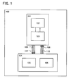
- FIG. 1 shows a block diagram of a semiconductor device on which a function of reducing power consumption is mounted in the present invention.
- a semiconductor device 100 has an arithmetic processing circuit 101 and a memory circuit 104.
- the arithmetic processing circuit 101 has an arithmetic circuit 102 and a control circuit 103.
- the memory circuit 104 has a ROM 105 and a RAM 106.
- the arithmetic processing circuit 101 and the memory circuit 104 are connected to each other by an address bus 107 and a data bus 108.
- An address bus signal 109 flowing in the address bus 107 is a signal which specifies the address in the memory circuit and is sent from the arithmetic processing circuit 101 to the memory circuit 104.
- a data bus signal 110 flowing in the data bus 108 is a signal for sending data of the address, which is specified by the address bus signal 109, in the memory circuit from the memory circuit 104 to the arithmetic processing circuit 101.
- ROM 105 In the ROM 105 provided in the memory circuit 104, data of a startup routine 230 and a machine language program 200 (also referred to as a main program) are stored, and in the RAM 106, processing data 210 obtained by executing the machine language program 200 is stored (see FIG. 2).
- a nonvolatile memory such as a mask ROM (Read Only Memory), an organic memory, or an EEPROM can be used
- the RAM 106 a volatile memory such as a static memory (SRAM: Static Random Access Memory) or a dynamic memory (DRAM: Dynamic Random Access Memory) can be used.
- SRAM Static Random Access Memory
- DRAM Dynamic Random Access Memory
- the data of the machine language program 200 stored in the ROM 105 is generated from a high-level language program 220 by a machine language program generation device (also referred to as a program conversion means) 221.
- the RAM 106 is divided into n banks, and the processing data 210 obtained by executing the machine language program 200 is divided into a plurality of stacks to be stored in the banks of the RAM.
- a first stack 204 of a first bank 201 to an m-th stack 240 of the first bank 201 are stored in the first bank 201
- a first stack 205 of a second bank 202 to an m-th stack 241 of the second bank 202 are stored in the second bank 202
- a first stack 206 of an n-th bank 203 to an m-th stack 242 of the n-th bank 203 are stored in the n-th bank 203.
- the RAM 106 has an address showing a place of data inside. The initial address starts from 0, and the number of the address increases as the size of the RAM 106 increases.
- the first bank 201 starts from a 0-th address and the n-th bank 203 ends with the last address. Further, the number of the address of the ROM 105 also increases as the size of the ROM 105 increases.
- the data of the startup routine 230 is added when the data of the machine language program 200, which is generated from the high-level language program 220 by the machine language program generation device 221, is stored in the ROM 105.
- an instruction is written, by which a first address (also referred to as a stack pointer) of the RAM 106 is set.
- the processing data 210 obtained by executing the machine language program 200 stored in the ROM 105 is stored in the RAM 106.
- the startup routine 230 is executed before the machine language program is operated.
- the first stack 204 of the first bank 201 is a first stack pointer. Therefore, when the machine language program 200 is executed, the arithmetic circuit uses subsequent stacks of the first stack 204 of the first bank 201 to store the processing data 210.
- the arithmetic processing circuit 101 included in the semiconductor device 100 starts operation (S400)
- the arithmetic processing circuit 101 outputs "0" to the address bus 107 as the address bus signal 109, and reads the startup routine 230 of the ROM 105 starting from an address "0" as the data bus signal 110 through the data bus 108 (S401).
- the arithmetic circuit 102 in the arithmetic processing circuit analyzes and executes data included in the startup routine 230 (S402).
- the arithmetic circuit 102 sets a stack pointer in order to store subsequent processing data (S403).
- the arithmetic circuit 102 executes the machine language program 200 (S404), and terminates the operation (S405).
- the processing data 210 obtained by executing the machine language program 200 of the ROM 105 is divided into a plurality of stacks to be stored in the RAM 106 provided with a plurality of (here, n) banks.
- a stack which is not used until the machine language program 200 is terminated that is, a stack of which data is not read until the machine language program 200 is terminated, is omitted.
- the machine language program is optimized so that stacks with contiguous writing are written to the same bank. As a result, power consumption of the memory circuit and the semiconductor device can be reduced.
- the machine language program generation device 221 includes a lexical analysis means 300, a syntactic analysis means 301, a semantic analysis means 302, a code generation means 303, a stack analysis means 304, and an optimization means 305 (see FIG. 3).
- the high-level language program 220 is decomposed into a token sequence 310 (also referred to as an element) by the lexical analysis means 300, relation of tokens in the token sequence 310 is analyzed by the syntactic analysis means 301, and a syntax tree 311 is built. Then, an intermediate language 312 is produced based on the syntax tree 311 by the semantic analysis means 302.
- the intermediate language 312 is converted into an executable code 313, which can be executed by the arithmetic processing circuit 101, by the code generation means 303.
- the stack analysis means 304 analyzes the executable code 313 and a status of use of the stack is examined and outputs an analysis result 320.
- the optimization means 305 optimizes the executable code 313 in accordance with the analysis result 320, makes the executable code 313 be a machine language program 200, and outputs the machine language program 200.
- FIG 5 shows a flowchart of the lexical analysis means 300.
- processing is performed, in which the high-level language program 220 is processed to be decomposed into a token sequence 310 including a plurality of tokens.
- the lexical analysis means 300 starts operation (S500)
- the lexical analysis means 300 reads a high-level language program 220 (S501).
- the lexical analysis means 300 reads a token dictionary compatible with the high-level language program 220 (S502).
- the lexical analysis means 300 searches in the high-level language program 220 with reference to the token dictionary which has been read, and a portion which matches a reference token in the token dictionary is extracted as a token (S503).
- the lexical analysis means 300 outputs the token sequence 310 (S505), and terminates the operation (S506).
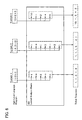
- FIG. 6 specifically shows processing by the lexical analysis means 300.
- Table 1 shows a high-level language program herein used as an example and a result of the processing. Since there are many kinds of reference tokens, as an example, numeric values, parentheses, and operators (+, -, *) are used as reference tokens here. It is to be noted that the numeric value is expressed by decimal notation, and tokens in a sequence are separated by commas.
- the lexical analysis means 300 When a high-level language program "1+2+3" of an example 1 in Table 1 is processed by the lexical analysis means 300, the lexical analysis means 300 reads a token dictionary in S502 of FIG 5. Subsequently, the lexical analysis means 300 compares a reference token and the high-level language program in S503 of FIG. 5, and a portion of the high-level language program which matches the reference token first is extracted as a token sequence. Here, specifically, the numeric value "1" is extracted as a token.
- the lexical analysis means 300 checks whether the high-level language program remains or not in S504 of FIG 5, and if the high-level language program remains, the lexical analysis means 300 compares the reference token and the high-level language program with each other again in S503 of FIG. 5.
- the high-level language program "+2+3" remains; therefore, the lexical analysis means 300 compares the reference token and the high-level language program with each other again, and the operator "+” is extracted as a token.
- tokens "2", "+", and "3" are extracted.
- checking is performed whether the high-level language program remains or not.
- the lexical analysis means 300 outputs a token sequence "1, +, 2, +, 3", and terminates the processing.
- the lexical analysis means 300 When a high-level language program "1+(3-2)" of an example 2 in Table 1 is processed by the lexical analysis means 300, the lexical analysis means 300 reads a token dictionary in S502 of FIG. 5. Subsequently, the lexical analysis means 300 compares a reference token and the high-level language program in S503 of FIG. 5, and a portion of the high-level language program which matches the reference token first is extracted as a token sequence. Here, specifically, the numeric value "1" is extracted as a token. Then, the lexical analysis means 300 checks whether the high-level language program remains or not in S504 of FIG.
- the lexical analysis means 300 compares the reference token and the high-level language program with each other again in S503 of FIG. 5.
- the high-level language program "+(3-2)" remains; therefore, the lexical analysis means 300 compares the reference token and the high-level language program with each other again, and the operator "+” is extracted as a token.
- tokens "(", "3", "-", "2", and ")" are extracted.
- checking is performed whether the high-level language program remains or not.
- the lexical analysis means 300 outputs a token sequence "1, +, (, 3, -, 2, )", and terminates the processing.
- the lexical analysis means 300 When a high-level language program "10-2*3" of an example 3 in Table 1 is processed by the lexical analysis means 300, the lexical analysis means 300 reads a token dictionary in S502 of FIG. 5. Subsequently, the lexical analysis means 300 compares a reference token and the high-level language program in S503 of FIG. 5, and a portion of the high-level language program which matches the reference token first is extracted as a token sequence. Here, specifically, the numeric value "10" is extracted as a token. Then, the lexical analysis means 300 checks whether the high-level language program remains or not in S504 of FIG.
- the lexical analysis means 300 compares the reference token and the high-level language program with each other again in S503 of FIG 5.
- the high-level language program "-2*3" remains; therefore, the lexical analysis means 300 compares the reference token and the high-level language program with each other again, and the operator "-" is extracted as a token.
- tokens "2", "*", and "3" are extracted.
- checking is performed whether the high-level language program remains or not.
- the lexical analysis means 300 outputs a token sequence "10, -, 2, *, 3", and terminates the processing.
- FIG. 7 shows a flowchart of the syntactic analysis means 301.
- relation of tokens is analyzed using a structure expressed by a tree (also referred to as a syntax tree).
- a tree also referred to as a syntax tree.
- the syntactic analysis means 301 starts operation (S700)
- the syntactic analysis means 301 reads a token sequence (S701).
- the syntactic analysis means 301 reads a token classification dictionary (S702).
- the syntactic analysis means 301 adds a comment to the token sequence in accordance with the token classification dictionary (S703), and reads a token priority level dictionary (S704).
- the syntactic analysis means 301 arranges tokens in the token sequence in accordance with the token priority level dictionary to build a syntax tree (S705). Finally, the syntactic analysis means 301 outputs the syntax tree (S706), and terminates the operation (S707).
- the syntax tree is such that tokens analyzed by the syntactic analysis means 301 are arranged in a tree shape.
- FIG. 8 specifically shows processing by the syntactic analysis means 301.
- the priority level of tokens here is priority-ordered in such a way that "a formula”, “an operator (*)", “an operator (+, -)”, and “a numeric value” in decreasing priority order, as an example.
- an antecedent token is considered to have a higher priority.
- the numeric value is expressed by decimal notation, and tokens in a sequence are separated by commas.
- the syntactic analysis means 301 When a token sequence "1, +, 2, +, 3" of an example 1 in FIG. 8 is processed by the syntactic analysis means 301, the syntactic analysis means 301 reads a token classification dictionary in S702 of FIG. 7. The syntactic analysis means 301 adds a comment to a token in the token sequence in accordance with its kind in S703 of FIG. 7. Specifically, the token sequence "1, +, 2, +, 3" becomes "a numeric value 1, an operator +, a numeric value 2, an operator +, a numeric value 3". Then, the syntactic analysis means 301 reads the token priority level dictionary in S704 of FIG. 7.
- the syntactic analysis means 301 converts the tokens into a syntax tree from the token having a higher priority level, based on the comment added to the token sequence. Specifically, since an operator + 810 has the highest priority level among them, a partial syntax tree 800 in the syntax tree is created first. The similar operation is repeated until the token sequence runs out, and the processing is terminated when the remaining token sequence runs out.
- the syntactic analysis means 301 When a token sequence "1, +, (, 3, -, 2, )" of an example 2 in FIG 8 is processed by the syntactic analysis means 301, the syntactic analysis means 301 reads a token classification dictionary in S702 of FIG. 7. The syntactic analysis means 301 adds a comment to a token in the token sequence in accordance with its kind in S703 of FIG. 7. Specifically, the token sequence "1, +, (, 3, -, 2, )" becomes "a numeric value 1, an operator +, a formula (, a numeric value 3, an operator -, a numeric value 2)". Then, the syntactic analysis means 301 reads the token priority level dictionary in S704 of FIG. 7.
- the syntactic analysis means 301 changes the tokens into a syntax tree from the token having a higher priority level, based on the comment added to the token sequence. Specifically, since an operator - 811 in the formula (a numeric value 3, an operator -, a numeric value 2) has the highest priority level, a partial syntax tree 801 in the syntax tree is created first. The similar operation is repeated until the token sequence runs out, and the processing is terminated when the remaining token sequence runs out.
- the syntactic analysis means 301 When a token sequence "10, +, 2, *, 5" of an example 3 in FIG. 8 is processed by the syntactic analysis means 301, the syntactic analysis means 301 reads a token classification dictionary in S702 of FIG 7. The syntactic analysis means 301 adds a comment to a token in the token sequence in accordance with its kind in S703 of FIG. 7. Specifically, the token sequence "10, +, 2, *, 5" becomes "a numeric value 10, an operator +, a numeric value 2, an operator *, a numeric value 5". Then, the syntactic analysis means 301 reads the token priority level dictionary in S704 of FIG 7.
- the syntactic analysis means 301 converts the tokens into a syntax tree from the token having a higher priority level, based on the comment added to the token sequence. Specifically, since an operator * 812 has the highest priority level among them, a partial syntax tree 802 in the syntax tree is created first. The similar operation is repeated until the token sequence runs out, and the processing is terminated when the remaining token sequence runs out.
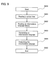
- FIG 9 shows a flowchart of the semantic analysis means 302.
- an intermediate language 312 is generated based on a syntax tree 311.
- the semantic analysis means 302 starts operation (S900)
- the semantic analysis means 302 reads a syntax tree (S901).
- the semantic analysis means 302 reads an intermediate language library (S902).
- the semantic analysis means 302 generates an intermediate language sequentially from a branch (lower portion) of a syntax tree 311 in accordance with the intermediate language library (S903).
- the semantic analysis means 302 outputs an intermediate language 312 (S904), and terminates the operation (S905).
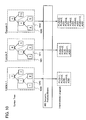
- FIG. 10 specifically shows processing by the semantic analysis means 302.
- the arithmetic processing ciruit 101 applies a stack method to the RAM 106 when the machine language program 200 is executed by the arithmetic processing circuit 101. Therefore, an intermediate language is written using a stack machine type.
- the semantic analysis means 302 reads the intermediate language library in S902 of FIG. 9 and generates an intermediate language (S903). Specifically, the semantic analysis means 302 makes a branchlet 1010 of the syntax tree be an intermediate language first.
- the intermediate language of the branchlet 1010 of the syntax tree is "PUSH1, PUSH2, ADD", which means that 1 and 2 are put into stacks and addition is performed.
- the semantic analysis means 302 converts the entire syntax tree into an intermediate language, outputs an intermediate language "PUSH1, PUSH2, ADD, PUSH3, ADD" in S904 of FIG. 9, and terminates the operation (S905).
- the semantic analysis means 302 reads the intermediate language library in S902 of FIG. 9 and generates an intermediate language (S903). Specifically, the semantic analysis means 302 makes a branchlet 1011 of the syntax tree be an intermediate language first.
- the intermediate language of the branchlet 1011 of the syntax tree is "PUSH3, PUSH2, SUB", which means that 3 and 2 are put into stacks and subtraction is performed.
- the semantic analysis means 302 converts the entire syntax tree into an intermediate language, outputs an intermediate language "PUSH3, PUSH2, SUB, PUSH1, ADD" in S904 of FIG. 9, and terminates the operation (S905).
- the semantic analysis means 302 When a syntax tree 1002 of an example 3 in FIG. 10 is processed by the semantic analysis means 302, the semantic analysis means 302 reads the intermediate language library in S902 of FIG. 9 and generates an intermediate language (S903). Specifically, the semantic analysis means 302 makes a branchlet 1012 of the syntax tree be an intermediate language first.
- the intermediate language of the branchlet 1012 of the syntax tree is "PUSH2, PUSH2, ADD, PUSH2, ADD, PUSH2, ADD, PUSH2, ADD, PUSH2, ADD", which means that 2 is put into a stack and addition is performed, and this opearation is repeated five times, that is, 2 times 5.
- the semantic analysis means 302 converts the entire syntax tree into an intermediate language, outputs an intermediate language "PUSH2, PUSH2, ADD, PUSH2, ADD, PUSH2, ADD, PUSH2, ADD, PUSH 10, ADD" in S904 of FIG. 9, and terminates the operation (S905).
- FIG. 11 shows a flowchart of the code generation means 303.
- an executable code 313 is generated based on the intermediate language 312.
- the code generation means 303 starts operation (S1100)
- the code generation means 303 reads an intermediate language (S1101).
- the code generation means 303 reads a code library (S1102).
- the code generation means 303 generates an executable code in accordance with the code library (S1103).
- the code generation means 303 outputs an executable code 313 (S1104), and terminates the operation (S1105).
- Table 2 shows a result of processing by the code generation means 303 as an example.
- an intermediate language is converted into an executable code (also referred to as a native code or an object code) which can be executed by the arithmetic processing circuit.
- the executable code is expressed by binary notation, and the numeric value of the intermediate language is expressed by decimal notation.
- FIG. 12 specifically shows processing by the stack analysis means 304.
- the stack analysis means 304 analyzes the executable code 313 and outputs an analysis result 320.
- FIG. 12 shows an analysis result in the stack analysis means as an example.
- execution time of the executable code 313 is on the horizontal axis and a stack pointer is on the vertical axis
- a status of movement of the stack pointer from a program start 1201 to a program termination 1202, that is, a status of use of the stacks is shown as a graph 1200.
- a bank boundary 1205 is a boundary between a first bank and a second bank, and similarly, a boundary between the second bank and a third bank is referred to as a bank boundary 1206, and a boundary between the third boundary and a fourth boundary is referred to as a bank boundary 1207.
- Contiguous stacks 1210 are particularly referred to as contiguous stacks which do not cross banks because writing to stacks is consecutively performed four times and the stacks do not cross the bank boundary 1205 or the bank boundary 1206.
- contiguous stacks 1211 are particularly referred to as contiguous stacks which cross banks, which are distinguished from the contiguous stacks 1210, because writing to a stack is consecutively performed four times and the stacks cross the bank boundary 1207.
- FIG 13 shows a flowchart of the optimization means 305.
- the optimization means 305 optimizes the executable code 313 in accordance with the analysis result 320 obtained by analyzing the executable code 313, makes the executable code 313 be a machine language program 200, and the optimization means 305, and outputs the machine language program 200.
- the optimization means 305 starts operation (S1300)
- the optimization means 305 reads an executable code (S1301).
- the optimization means 305 reads RAM design information (S1302).
- RAM design information is, specifically, information on the bank size of a RAM.
- the optimization means 305 reads the analysis result 320 (S1303), and optimization is performed so that power consumption of the RAM is reduced (S1304).
- stacks of which data are not read until the program is terminated are omitted, and stacks are arranged so that, among stacks of which data are read, stacks with contiguous writing do not cross a boundary between banks.
- the optimization means 305 outputs a machine language program 200 (S1305), and terminates the operation (S1306).
- FIG. 14 specifically shows processing by the optimization means 305.
- the executable code is expressed by binary notation. As an example, description is given under the condition where the number of banks n is set to 4 and the number of stacks m is set to 4, and the graph 1200 shown in FIG 12 is used as the analysis result.
- the optimization means When an executable code 1401 in FIG. 14 is processed by the optimization means, the optimization means reads the executable code 1401 in S1301 of FIG. 13 and reads the RAM design information in S1302 of FIG. 13. Specifically, since the number of banks n is set to 4 and the number of stacks m is set to 4 in this embodiment mode, the optimization means reads such RAM design information. Then, the optimization means reads the graph 1200 and performs optimization so that power consumption of the RAM is reduced (S1304).
- stacks 1410 which are not used until the program is terminated are omitted (graph 1405), and subsequently, stacks 1420 with contiguous writing are rearranged so as not to cross a first bank boundary 1430 (graph 1406).
- the stacks 1420 with contiguous writing are arranged so that writing is performed between the first bank boundary 1430 (a boundary between a first bank and a second bank) and a second bank boundary 1440 (a boundary between the second bank and a third bank).
- the sentence "stacks are omitted" means that stacks in which data is once written are used for performing writing of the data to the stacks. Thus, the number of stacks used for writing of data can be reduced.
- the optimization means 305 optimizes an executable code in accordance with the graph 1406. Finally, the optimization means 305 outputs a machine language program 1402 in S1305 of FIG. 13, and terminates the operation (S1306).
- the machine language program 200 is stored in the ROM 105 and is executed by the arithmetic processing circuit. Power consumption for writing or reading becomes lower as the address of the stack pointer becomes lower. Accordingly, by executing such a machine language program by the arithmetic processing circuit, power consumption can be reduced.
- a machine language program suitable for a memory circuit which is generated by a machine language program generation device, is executed, whereby power consumption can be reduced. Accordingly, a high-performance semiconductor device consuming low power can be provided. Further, in a semiconductor device including an arithmetic processing circuit and a memory circuit, since optimization of an executable code of a program can be attempted, it is not necessary to remake the semiconductor device again from the stage of mask design due to change in specification in accordance with change in method of operation. Therefore, manufacturing cost can be reduced and manufacturing time can be shortened. Furthermore, since the mask design is not changed, there is no concern that a semiconductor device manufactured after changing the mask design will malfunction.
- a memory in this embodiment mode refers to a RAM in Embodiment Mode 1.
- one memory block in this embodiment mode is the same as one bank in Embodiment Mode 1.
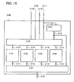
- FIG. 15 is a block diagram of a memory of this embodiment mode.
- FIG. 16 is a block diagram of a memory block included in the memory of this embodiment mode.
- FIG. 17 is a timing chart of the memory block included in the memory of this embodiment mode.
- FIG. 18 is a timing chart of the memory of this embodiment mode.
- a memory 2100 of this embodiment mode includes first to fourth memory blocks 2101 to 2104, an operation control circuit 2105, an input signal control circuit 2106, and an output signal control circuit 2107. Note that each of the first to fourth memory blocks 2101 to 2104 is a memory block 2200 in FIG. 16.
- a memory address signal is 4 bits, that is, 16 words, and a memory reading/writing data signal is 4 bits.
- the memory block 2200 includes a memory array 2201, a row decoder 2202, and an RW circuit 2203.
- the memory array 2201 includes first to sixteenth memory cells 2204 to 2219, which are arranged in a four-by-four matrix.
- a first reading word signal line 2224 and a first writing word signal line 2228 are each electrically connected to the first to fourth memory cells 2204 to 2207; a second reading word signal line 2225 and a second writing word signal line 2229 are each electrically connected to the fifth to eighth memory cells 2208 to 2211; a third reading word signal line 2226 and a third writing word signal line 2230 are each electrically connected to the ninth to twelfth memory cells 2212 to 2215; and a fourth reading word signal line 2227 and a fourth writing word signal line 2231 are each electrically connected to the thirteenth to sixteenth memory cells 2216 to 2219.
- a first reading bit signal line 2232 and a first writing bit signal line 2236 are each electrically connected to the first, fifth, ninth, and thirteenth memory cells 2204, 2208, 2212, and 2216; a second reading bit signal line 2233 and a second writing bit signal line 2237 are each electrically connected to the second, sixth, tenth, and fourteenth memory cells 2205, 2209, 2213, and 2217; a third reading bit signal line 2234 and a third writing bit signal line 2238 are each electrically connected to the third, seventh, eleventh, and fifteenth memory cells 2206, 2210, 2214, and 2218; and a fourth reading bit signal line 2235 and a fourth writing bit signal line 2239 are each electrically connected to the fourth, eighth, twelfth, and sixteenth memory cells 2207, 2211, 2215, and 2219.
- the first to fourth reading bit signal lines 2232 to 2235 come to have high potentials or low potentials depending on data stored in the first to fourth memory cells 2204 to 2207.
- a potential of the first writing word signal line 2228 is "H"
- data is stored in the first to fourth memory cells 2204 to 2207, depending on potentials of the first to fourth writing bit signal lines 2236 to 2239.
- the row decoder 2202 has a function of generating first to fourth reading word signals supplied to the first to fourth reading word signal lines 2224 to 2227 and first to fourth writing word signals supplied to the first to fourth writing word signal lines 2228 to 2231, in response to first and second memory block address signals, a memory block reading control signal, and a memory block writing control signal supplied from first and second memory block address signal lines 2220 and 2221, a memory block reading control signal line 2222, and a memory block writing control signal line 2223, respectively.
- the row decoder 2202 has a function of making the first, second, third, and fourth reading word signals be "H"
- the memory block reading control signal is "H” and combinations of potentials of the first memory block address signal and the second memory block address signal are "LL", “LH”, “HL”, and “HH", respectively.
- the memory block reading control signal is "H”
- a potential of the first memory block address signal is "L”
- a potential of the second memory block address signal is "H”
- the second reading word signal is made to be "H”.
- the row decoder 2202 has a function of making the first, second, third, and fourth writing word signals be "H"
- the memory block writing control signal is "H” and combinations of potentials of the first memory block address signal and the second memory block address signal are "LL", “LH”, “HL”, and “HH", respectively.
- the memory block writing control signal is "H”
- a potential of the first memory block address signal is "L”
- a potential of the second memory block address signal is "H”
- the second writing word signal is made to be "H”.
- H denotes a high potential
- L denotes a low potential
- the RW circuit 2203 has a function of generating first to fourth memory block reading data signals, which are to be supplied to the first to fourth memory block reading data signal lines 2240 to 2243, from first to fourth reading bit signals supplied to the first to fourth reading bit signal lines 2232 to 2235, depending on data stored in the memory cells. Also, the RW circuit 2203 has a function of generating first to fourth writing bit signals, which are to be supplied to the first to fourth writing bit signal lines 2236 to 2239, from first to fourth memory block writing data signals supplied from first to fourth memory block writing data signal lines 2244 to 2247.
- the RW circuit 2203 quickly detects with a sense amplifier whether the first to fourth reading bit signal lines 2232 to 2235 have high potentials or low potentials, and generates the first to fourth memory block reading data signals to be supplied to the first to fourth memory block reading data signal lines 2240 to 2243, through a latch and a buffer. Further, the RW circuit 2203 generates the first to fourth writing bit signals to be supplied to the first to fourth writing bit signal lines 2236 to 2239, depending on potentials of the first to fourth memory block writing data signal lines 2244 to 2247.
- FIG. 17 is a timing chart relating to an input/output signal of the memory block 2200.
- a timing chart of the first memory block address signal supplied from the first memory block address signal line 2220 in FIG. 16 is shown by a first signal 2351 in FIG 17.
- a timing chart of the second memory block address signal supplied from the second memory block address signal line 2221 in FIG. 16 is shown by a second signal 2352 in FIG 17.
- a timing chart of the memory block reading control signal supplied from the memory block reading control signal line 2222 and a timing chart of the memory block writing control signal supplied from the memory block writing control signal line 2223 in FIG 16 are shown by a third signal 2353 and a fourth signal 2354 in FIG 17, respectively.
- timing charts of the first to fourth memory block writing data signals which are supplied from the first to fourth memory block writing data signal lines 2244 to 2247 in FIG. 16, respectively, are shown by fifth to eighth signals 2355 to 2358 in FIG. 17, respectively.
- the RW circuit 2203 has a function of generating the first to fourth writing bit signals from the first to fourth memory block writing data signals, via a buffer.
- timing charts of the first to fourth writing bit signals supplied to the first to fourth writing bit signal lines 2236 to 2239 are similar to the timing charts of the fifth to eighth signals 2355 to 2358 in FIG. 17.
- a period in which a memory block writing control signal is "H”, that is, a first period 2371 in FIG. 17, is to be a memory block writing period.
- a period in which the memory block reading control signal is "H”, that is, a third period 2373 in FIG. 17, is to be a memory block reading period.
- a period in which the memory block reading control signal and the memory block writing control signal are both "L”, that is, a second period 2372 in FIG. 17, is to be a memory block waiting period.
- the first, second, third, and fourth writing word signals become “H”.
- the first, second, third, and fourth writing word signals refer to signals supplied from the first, second, third, and fourth writing word signal lines 2228, 2229, 2230, and 2231, respectively. Accordingly, timing charts of the first to fourth writing word signals become like those of ninth to twelfth signals 2359 to 2362 in FIG. 17.
- a memory block reading period 2373 in a case where the memory block reading control signal supplied from the memory block reading control signal line 2222 in FIG. 16 is "H", the first, second, third, and fourth reading word signals become “H” when the first memory block address signal and the second memory block address signal, which are supplied from the first memory block address signal line 2220 and the second memory block address signal line 2221, respectively, are "LL", “LH”, "HL”, and "HH", respectively.
- the first, second, third, and fourth reading word signals refer to signals supplied from the first, second, third, and fourth reading word signal lines 2224, 2225, 2226, and 2227, respectively. Accordingly, timing charts of the first to fourth reading word signals become like those of thirteenth to sixteenth signals 2363 to 2366 in FIG. 17.
- the first to fourth reading bit signals are supplied to the first to fourth reading bit signal lines 2232 to 2235, depending on potentials stored in the first to fourth memory cells 2204 to 2207 in FIG. 16.
- the first to fourth reading bit signals become "H”, "H", "L”, and "L".
- the first to fourth reading bit signals are supplied to the first to fourth reading bit signal lines 2232 to 2235, depending on potentials stored in the fifth to eighth memory cells 2208 to 2211 in FIG. 16.
- the first to fourth reading bit signals become "L”, "L”, "H", and "H".
- the first to fourth reading bit signals are supplied to the first to fourth reading bit signal lines 2232 to 2235, depending on potentials stored in the ninth to twelfth memory cells 2212 to 2215 in FIG. 16.
- the first to fourth reading bit signals become "H", "L", "L”, and "H".
- the first to fourth reading bit signals are supplied to the first to fourth reading bit signal lines 2232 to 2235, depending on potentials stored in the thirteenth to sixteenth memory cells 2216 to 2219 in FIG. 16.
- the first to fourth reading bit signals become "L”, "H", "H", and "L".
- timing charts of the first to fourth reading bit signals are seventeenth to twentieth signals 2367 to 2370 in FIG. 17.
- the RW circuit 2203 has a function of generating the first to fourth memory block reading data signals from the first to fourth reading bit signals, via a buffer.
- timing charts of the first to fourth memory block reading data signals supplied to the first to fourth memory block reading data signal lines 2240 to 2243 are also similar to timing charts of the seventeenth to twentieth signals 2367 to 2370 in FIG. 17.
- memory block input signals that is, the first and second memory block address signals, the memory block reading control signal, the memory block writing control signal, and the memory block writing data signal
- the memory block input signals have a constant value.
- power consumption can be significantly reduced.
- each of the first to fourth memory blocks 2101 to 2104 in FIG. 15 is the memory block 2200 in FIG. 16.
- input signal lines of the first memory block 2101 are first memory block input signal lines 113 in FIG 15, which are the first and second memory block address signal lines 2220 and 2221, the memory block reading control signal line 2222, the memory block writing control signal line 2223, and the first to fourth memory block writing data signal lines 2244 and 2247 in FIG. 16.
- output signal lines of the first memory block 2101 are first memory block output signal lines 2117 in FIG. 15, which are the first to fourth memory block reading data signal lines 2240 to 2243 in FIG. 16.
- input signal lines of the second to fourth memory blocks 2102 to 2104 are second to fourth memory block input signal lines 2114 to 2116 in FIG. 15, which are each the first and second memory block address signal lines 2220 and 2221, the memory block reading control signal line 2222, the memory block writing control signal line 2223, and the first to fourth memory block writing data signal lines 2244 and 2247 in FIG. 16.
- output signal lines from the second to fourth memory blocks 2102 to 2104 are second to fourth memory block output signal lines 2118 to 2120 in FIG. 15, which are each the first to fourth memory block reading data signal lines 2240 to 2243 in FIG. 16.
- the operation control circuit 2105 has a function of generating first to fourth memory block operation control signals from the third and the fourth memory address signals among first to fourth memory address signals supplied from a memory address bus signal line 2111 including the first to fourth memory address signal lines. According to a potential of each of the foregoing first to fourth memory block operation control signals, operation of each of the first to fourth memory blocks 2101 to 2104 is controlled. Note that the first to fourth memory block operation control signals are supplied to a memory block operation control bus signal line 112 including first to fourth memory block operation control signal lines.
- the third memory address signal and the fourth memory address signal are each "LL"
- a memory cell to be read from or written to is included in the first memory block 2101.
- the third memory address signal and the fourth memory address signal are "LH”, "HL”, and "HH”, respectively
- a memory cell to be read from or written to is included in the second memory block 2102, the third memory block 2103, and the fourth memory block 2104, respectively. That is, in a case where the third memory address signal is "L” and the fourth memory address signal is "H", the memory cell to be read from or written to is in the second memory block 2102.
- the first memory block operation control signal is "H”
- each of the second, third, and fourth memory block operation control signals is “L”.
- the second, third, and fourth memory block operation control signals are each "H", while other memory block operation control signals are "L”.
- the third memory address signal is "L”
- the fourth memory address signal is "L”
- the first memory block operation control signal is "H”
- the rest thereof that is, the second to fourth memory block operation control signals are each "L".
- the input signal control circuit 2106 has a function of generating first to fourth memory block input signals, from a memory reading control signal; a memory writing control signal; first to fourth memory writing data signals; the first and second memory address signals; and the first to fourth memory block operation control signals, supplied from a memory reading control signal line 2108; a memory writing control signal line 2109; a memory writing data bus signal line 2110 including the first to fourth memory writing data signal lines; the memory address bus signal line 2111, and the memory block operation control bus signal line 2112; respectively.
- the first to fourth memory block input signals are supplied to the first to fourth memory block input signal lines 2113 to 2116, respectively.
- the first memory block operation control signal is "H"
- potentials corresponding to the memory reading control signal, the memory writing control signal, the first to fourth memory writing data signals, and the first and second memory address signals become the first memory block input signal.
- the second, third, and fourth memory block input signals are to have a constant value independent of values of the memory reading control signal, the memory writing control signal, the memory writing data signals, and the memory address signals.
- the potentials corresponding to the memory reading control signal, the memory writing control signal, the first to fourth memory writing data signal, and the first and second memory address signals are the second memory block input signal when the second memory block operation control signal is "H", the third memory block input signal when the third memory block operation control signal is "H”, and the fourth memory block input signal when the fourth memory block operation control signal is "H”.
- other memory block input signals are to have a constant value independent of values of the memory reading control signal, the memory writing control signal, the memory writing data signal, and the memory address signal.
- the output signal control circuit 2107 has a function of generating first to fourth memory reading data signals to be supplied to a memory reading data bus signal line 2121 including first to fourth memory reading data signal lines, from first to fourth memory block output signals supplied from the first to fourth memory block output signal lines 2117 to 2120 and first to fourth memory block operation control signals supplied from the memory block operation control bus signal line 2112.
- any one of the first to fourth memory block output signals is selected depending on the first to fourth memory block operation control signals, and via a buffer, the memory block output signal is supplied to the memory reading data bus signal line 2121 as a memory reading data signal.
- FIG. 18 is a timing chart relating to an input/output signal of a memory in this embodiment mode.
- the timing charts of the first to fourth memory address signals; the memory reading control signal; the memory writing control signal; and the first to fourth memory writing data signals supplied from the memory address bus signal line 2111; the memory reading control signal line 2108; the memory writing control signal line 2109; and the memory writing data bus signal line 2110 in FIG. 15, respectively, are first to fourth signals 2401 to 2404 in FIG. 18, respectively. Note that potentials of the first to fourth memory address signals are sequentially marked to represent the first signal 2401. Similarly, potentials of the first to fourth memory writing data signals are sequentially marked to represent the fourth signal 2404.
- a period in which a memory writing control signal is "H”, that is, a first period 2418 in FIG. 18, is to be a memory writing period.
- a period in which the memory reading control signal is "H”, that is, a third period 2420 in FIG. 18, is to be a memory reading period.
- a period in which the memory reading control signal and the memory writing control signal are both "L”, that is, a second period 2419 in FIG. 18, is to be a memory waiting period.
- the first memory block operation control signal becomes “H”
- each of the second, third, and fourth memory block operation control signals becomes “L”.
- the second memory block operation control signal becomes "H” in a case where a combination of potentials of the third memory address signal and the fourth memory address signal is "LH”, while each of the first, third, and fourth memory block operation control signals becomes “L”.
- the third memory block operation control signal becomes "H” in a case where a combination of potentials of the third memory address signal and the fourth memory address signal is "HL”, while each of the first, second, and fourth memory block operation control signals becomes “L”.
- the fourth memory block operation control signal becomes "H” in a case where a combination of potentials of the third memory address signal and the fourth memory address signal is "HH", while each of the first, second, and third memory block operation control signals becomes “L". Accordingly, timing charts of the first and second memory block operation control signals become like those of fifth and sixth signals 405 and 406 in FIG 18. Note that although timing charts of the third and fourth memory block operation control signals are not shown in FIG 18, they are constantly "L".
- the input signal control circuit 2106 in FIG. 15 generates the first to fourth memory block input signals by carrying out a logical AND operation with respect to the memory reading control signal, the memory writing control signal, the first to fourth memory writing data signals, and the first and second memory address signals, with the first, second, third, and fourth memory block operation control signals, respectively. That is, in a period in which the first memory block operation control signal is "H", the memory reading control signal, the memory writing control signal, the first to fourth memory writing data signals, and the first and second memory address signals become the first memory block input signal, and all of the second to fourth memory block input signals become "L".
- timing charts of the first and second memory block address signals in the first memory block 2101 are a seventh signal 2407 in FIG. 18, a timing chart of the memory block reading control signal is an eighth signal 2408 in FIG. 18, a timing chart of the memory block writing control signal is a ninth signal 2409 in FIG 18, and timing charts of the first to fourth memory block writing data signals are a tenth signal 2410 in FIG 18.
- potentials of the first and second memory block address signals are sequentially marked to represent the seventh signal 2407.
- potentials of the first to fourth block writing data signals are sequentially marked to represent the tenth signal 2410.
- Data stored in the first memory block 2101 during a memory writing period is read during a memory reading period. Accordingly, a timing chart of the first memory block reading data signal is an eleventh signal 2411 in FIG. 18.
- timing charts of the first and second memory block address signals in the second memory block 2102 are a twelfth signal 2412 in FIG 18, a timing chart of the memory block reading control signal is a thirteenth signal 2413 in FIG. 18, a timing chart of the memory block writing control signal is a fourteenth signal 2414 in FIG. 18, and timing chart of the first to fourth memory block writing data signals are a fifteenth signal 2415 in FIG. 18.
- potentials of the first and second memory block address signals are sequentially marked to represent the twelfth signal 2412.
- potentials of the first to fourth memory block writing data signals are sequentially marked to represent the fifteenth signal 2415.
- data stored in the second memory block 2102 during a memory writing period is read during a memory reading period. Accordingly, a timing chart of the second memory block reading data signal is a sixteenth signal 2416 in FIG. 18.
- the output signal control circuit 2107 in FIG. 15 selects the first memory block output signal when the first memory block operation control signal is "H”; the second memory block output signal when the second memory block operation control signal is “H”; the third memory block output signal when the third memory block operation control signal is “H”; and the fourth memory block output signal when the fourth memory block operation control signal is "H”; and makes the selected signals the first to fourth memory reading data signals, respectively.
- timing charts of the first to fourth memory reading data signals are a seventeenth signal 2417 in FIG. 18.
- power consumption in the first, third, and fourth memory blocks 2101, 2103, and 2104 are equal to power consumption in a waiting period. Consequently, at least three-fourths of the entire memory is constantly in a waiting state, and power consumption of the entire memory can be reduced significantly.
- SRAM static RAM
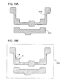
- Semiconductor layers 1510 and 1511 shown in FIG. 19A are preferably formed using silicon or a crystalline semiconductor including silicon as a component.
- silicon or a crystalline semiconductor including silicon as a component.
- polycrystalline silicon obtained by crystallizing a silicon film by laser annealing, monocrystalline silicon, or the like is applied.
- a metal oxide semiconductor, amorphous silicon, or an organic semiconductor exhibiting a semiconductor characteristic can be applied.
- a semiconductor layer formed first is formed over an entire surface of a substrate having an insulating surface or a portion thereof (a region having a larger area than a region that is set as a semiconductor region of a transistor). Then, a mask pattern is formed over the semiconductor layer by a photolithography technique. By subjecting the semiconductor layer to an etching treatment utilizing the mask pattern, the semiconductor layers 1510 and 1511 that are island-shaped, each including a source region, a drain region, and a channel formation region of a TFT, are formed. Shapes of the semiconductor layers 1510 and 1511 are decided in consideration of the appropriateness of a layout.
- a photomask for forming the semiconductor layers 1510 and 1511 shown in FIG. 19A has a mask pattern 1520 shown in FIG. 19B.
- This mask pattern 1520 differs depending on whether a resist used in a photolithography step is a positive-type or a negative-type.
- the mask pattern 1520 shown in FIG. 19B is formed as a light-shielding portion.
- the mask pattern 1520 has a polygonal shape where an apex A is removed.
- a bend portion B has a bent shape so that a corner portion thereof does not have a right angle.
- a right triangle with a side of 10 ⁇ m or less in a corner portion of the pattern is removed.
- a shape of the mask pattern 1520 shown in FIG. 19B is reflected on the semiconductor layers 1510 and 1511 shown in FIG. 19A.
- a shape similar to that of the mask pattern 1520 may be transferred, but the transferred shape may be a shape which has a rounder corner portion than that of the mask pattern 1520.
- the shape may be a smoother pattern shape than the shape of the mask pattern 1520, with a rounded portion.
- an insulating layer at least partially including silicon oxide or silicon nitride is formed over the semiconductor layers 1510 and 1511.
- One object for forming this insulating layer is to form a gate insulating layer.
- gate wirings 1612, 1613, and 1614 are formed so as to partially overlap with the semiconductor layers.
- the gate wiring 1612 is formed to correspond to the semiconductor layer 1510
- the gate wiring 1613 is formed to correspond to the semiconductor layers 1510 and 1511
- the gate wiring 1614 is formed to correspond to the semiconductor layers 1510 and 1511.
- the gate wirings are formed by forming a metal layer or a semiconductor layer with high conductivity and then shaping it over an insulating layer by a photolithography technique.
- a photomask for forming this gate wiring has a mask pattern 1621 shown in FIG 20B.
- a right triangle with a side of 10 ⁇ m or less or a triangle with a side having a length that is greater than or equal to 1/5 and less than or equal to 1/2 of a wiring width is removed from a corner portion of this mask pattern 1621.
- a shape of the mask pattern 1621 shown in FIG 20B is reflected on the gate wirings 1612, 1613, and 1614 shown in FIG. 20A. In that case, a shape similar to that of the mask pattern 1621 may be transferred, but the transferred shape may be a shape which has a rounder corner portion than that of the mask pattern 1621.
- the shape of the gate wirings may be a smoother pattern shape than the shape of the mask pattern 1621, with a rounded portion. That is, a corner portion of each of the gate wirings 1612, 1613, and 1614 is rounded off so that 1/5 to 1/2 of a wiring width is removed. Accordingly, tremendous improvement in yield can be realized as a result of a convex portion suppressing generation of fine powder due to abnormal electrical discharge when performing dry etching with plasma, and a concave portion washing away the fine powder easily collected at a corner when washing is performed, even if such fine powder is generated.
- An interlayer insulating layer is a layer formed after the gate wirings 1612, 1613, and 1614.
- the interlayer insulating layer is formed using an inorganic insulating material such as silicon oxide, or an organic insulating material that uses polyimide, an acrylic resin, or the like.
- an insulating layer of silicon nitride, silicon nitride oxide, or the like may be provided.
- an insulating layer of silicon nitride, silicon nitride oxide, or the like may also be provided over the interlayer insulating layer. This insulating layer can prevent contamination of the semiconductor layers or the gate insulating layer by an impurity such as an exogenous metal ion or moisture, which is not good for a TFT.
- an open portion is formed in a predetermined position.
- the open portion is provided to correspond to the gate wiring or semiconductor layer that is in a lower layer.
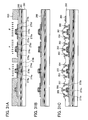
- a wiring layer which is formed of a single layer of a metal or a metal compound, or a plurality of layers thereof, is formed to have a prescribed pattern by an etching process using a mask pattern formed by a photolithography technique. Then, as shown in FIG 21A, wirings 1715 to 1720 are formed so as to partially overlap with the semiconductor layers.
- the wirings link specific elements.
- the wirings do not link the specific elements in a straight line, and there is a bend portion because of a limitation in terms of layout.
- a wiring width changes in a contact portion or in another region. In the contact region, in a case where a contact hole is as large as the wiring width or larger, the wiring width changes so as to be wider in the contact portion.
- a photomask for forming these wirings 1715 to 1720 has a mask pattern 1722 shown in FIG. 21B.
- a right triangle with a side of 10 ⁇ m or less or a triangle with a side having a length that is greater than or equal to 1/5 and less than or equal to 1/2 of a wiring width is removed from a corner portion of each of the wirings so that the corner portion has a rounded pattern.
- the corner portion is rounded off so that 1/5 to 1/2 of a wiring width is removed.
- n-channel thin film transistors 1721 to 1724 and p-channel thin film transistors 1725 and 1726 are formed.
- the n-channel thin film transistor 1723 and the p-channel thin film transistor 1725 form an inverter 1727
- the n-channel thin film transistor 1724 and the p-channel thin film transistor 1726 form an inverter 1728.
- a circuit including these six thin film transistors forms an SRAM.
- an insulating layer of silicon nitride, silicon oxide, or the like may be formed.
- a high-performance semiconductor element consuming low power can be provided to be lighter in weight and lower in cost.
- the transistor forming the semiconductor device of the present invention can include a thin film transistor (TFT) instead of a MOS transistor formed over a single crystalline substrate.
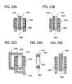
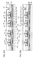
- FIG. 22 is a view showing a cross-sectional structure of a thin film transistor forming such circuits.
- an n-channel thin film transistor 1821, an n-channel thin film transistor 1822, a capacitor element 1824, a resistance element 1825, and a p-channel thin film transistor 1823 are shown.
- Each thin film transistor includes a semiconductor layer 1805, an insulating layer 1808, and a gate electrode 1809.
- the gate electrode 1809 is formed of a stacked structure of a first conductive layer 1803 and a second conductive layer 1802. Also, FIGS.
- 23A to 23E are top views of the n-channel thin film transistor 1821, the n-channel thin film transistor 1822, the capacitor element 1824, the resistance element 1825, and the p-channel thin film transistor 1823 shown in FIG. 22, respectively, which can also be referred to.
- an impurity region 1807 is formed on both sides of a gate electrode in the semiconductor layer 1805.
- the impurity region 1807 is also called a low-concentration drain (LDD) and is doped at a lower concentration than an impurity concentration of an impurity region 1806 formed as a source region or drain region which forms a contact with a wiring 1804.
- LDD low-concentration drain
- phosphorus or the like is added to the impurity region 1806 and the impurity region 1807 as an impurity imparting n-type conductivity.
- the LDD is formed as a means to suppress hot electron degradation or a short-channel effect.
- the first conductive layer 1803 is formed to expand past both sides of the second conductive layer 1802.
- a film thickness of the first conductive layer 1803 is thinner than a film thickness of the second conductive layer.
- the thickness of the first conductive layer 1803 is a thickness through which ion species that has accelerated in an electric field of 10 to 100 kV can pass through.
- the impurity region 1807 is formed to overlap with the first conductive layer 1803 of the gate electrode 1809. In other words, an LDD region that overlaps with the gate electrode 1809 is formed.
- the impurity region 1807 is formed in a self-aligned manner by adding an impurity imparting one conductivity type through the first conductive layer 1803 with the second conductive layer 1802 used as a mask. That is, the LDD overlapping with the gate electrode is formed in a self-aligned manner.
- a thin film transistor having an LDD on each side is applied to a rectifying TFT for a power source circuit or a thin film transistor forming a transmission gate (also called an analog switch) used for a logic circuit.
- An LDD is preferably provided on each side of a gate electrode for such TFTs, since both positive and negative voltages are applied to a source electrode or drain electrode.
- the first conductive layer 1803 may be patterned so that one side of the first conductive layer 1803 is aligned with one side of the second conductive layer 1802, and the other side of the first conductive layer 1803 is aligned with the other side of the second conductive layer 1802. As a result, a fine gate wiring can be formed. Also, it is not necessary that the LDD overlapping with the gate electrode be formed in a self-aligned manner.
- the impurity region 1807 doped at a lower concentration than an impurity concentration of the impurity region 1806 is formed on one side of the gate electrode in the semiconductor layer 1805.
- the first conductive layer 1803 is formed to expand past one side of the second conductive layer 1802.
- the LDD can be formed in a self-aligned manner by adding an impurity imparting one conductivity type through the first conductive layer 1803 with the second conductive layer 1802 used as a mask.
- a thin film transistor having an LDD on one side may be applied to a thin film transistor in which only a positive voltage or negative voltage is applied between a source electrode and a drain electrode. Specifically, it may be applied to a thin film transistor forming a logic gate such as an inverter circuit, a NAND circuit, a NOR circuit, or a latch circuit; or a thin film transistor forming an analog circuit such as a sense amplifier, a constant-voltage generating circuit, or a VCO.
- a logic gate such as an inverter circuit, a NAND circuit, a NOR circuit, or a latch circuit
- an analog circuit such as a sense amplifier, a constant-voltage generating circuit, or a VCO.
- the capacitor element 1824 is formed by interposing the insulating layer 1808 between the first conductive layer 1803 and the semiconductor layer 1805.
- the semiconductor layer 1805 for forming the capacitor element 1824 includes impurity regions 1810 and 1811.
- the impurity region 1811 is formed in the semiconductor layer 1805 in a position overlapping with the first conductive layer 1803.
- the impurity region 1810 forms a contact with the wiring 1804.
- the impurity region 1811 can be formed by adding an impurity imparting one conductivity type through the first conductive layer 1803; therefore, impurity concentrations of the impurity regions 1810 and 1811 can be made to be either the same or different.
- the resistance of the semiconductor layer 1805 is preferably lowered by adding an impurity imparting one conductivity type.
- the first conductive layer 1803 can fully function as an electrode by utilizing the second conductive layer 1802 as an auxiliary electrode as shown in FIG. 23C. In this manner, by forming a composite electrode structure where the first conductive layer 1803 and the second conductive layer 1802 are combined, the capacitor element 1824 can be formed in a self-aligned manner.
- the capacitor element is used as a storage capacitor included in a power source circuit of a wireless chip or a resonant capacitor included in a resonance circuit.
- a resonant capacitor needs to function as a capacitor regardless of whether a voltage between two terminals of the capacitor is positive or negative, since both positive and negative voltages are applied between the two terminals.
- the resistance element 1825 is formed of the first conductive layer 1803. Since the first conductive layer 1803 is formed with a thickness of about 30 to 150 nm, the resistance element can be formed by appropriately setting width and length of the first conductive layer 1803.
- the resistance element is used for a resistance load included in a modulation/demodulation circuit of a wireless chip. Also, the resistance element may also be used as a load in a case where current is controlled by a VCO or the like.
- the resistance element may be formed of semiconductor layer containing an impurity element at high concentration or a thin metal layer. The metal layer is preferable because variation in resistance elements can be small, since resistance is determined by few parameters such as film thickness and film quality, as opposed to the semiconductor layer resistance of which is dependent on film thickness, film quality, impurity concentration, activation rate, and the like.
- the p-channel thin film transistor 1823 includes an impurity region 1812 in the semiconductor layer 1805.
- This impurity region 1812 forms a source region or drain region which forms a contact with the wiring 1804.
- a structure of the gate electrode 1809 is such that the first conductive layer 1803 and the second conductive layer 1802 overlap with each other.
- the p-channel thin film transistor 1823 has a single drain structure in which an LDD is not provided.
- boron or the like is added to the impurity region 1812 as an impurity imparting p-type conductivity.
- an n-channel thin film transistor with a single drain structure is formed.
- One or both of the semiconductor layer 1805 and the insulating layer 1808 that functions as a gate insulating layer may be oxidized or nitrided by high-density plasma treatment with the conditions of microwave excitation, an electron temperature of less than or equal to 2 eV, an ion energy of less than or equal to 5 eV, and an electron density of approximately 10 11 to 10 13 /cm 3 .
- the layer in an oxygen atmosphere (e.g., O 2 , N 2 O, or the like) or a nitrogen atmosphere (e.g., N 2 , NH 3 , or the like) with the substrate temperature being set at 300 to 450°C, a defect level of an interface between the semiconductor layer 1805 and the insulating layer 1808 that functions as a gate insulating layer can be lowered.
- an oxygen atmosphere e.g., O 2 , N 2 O, or the like
- a nitrogen atmosphere e.g., N 2 , NH 3 , or the like
- an insulating layer oxidized or nitrided by the aforementioned plasma treatment can be used as the insulating layer 1808 that functions as a gate insulating layer.
- the insulating layer 1808 that functions as a gate insulating layer can be formed by combining an insulating layer formed over the surface of the semiconductor layer 1805 by the aforementioned plasma treatment with an insulating layer deposited by a CVD method (a plasma CVD method or a thermal CVD method).
- a CVD method a plasma CVD method or a thermal CVD method
- such an insulating layer can be utilized as a dielectric layer of the capacitor element 1824 as well.
- the insulating layer formed by the plasma treatment is a dense film with a thickness of 1 to 10 nm; therefore, a capacitor element with a high capacity can be formed.
- elements with various structures can be formed by combining conductive layers with various thicknesses.
- a region where only the first conductive layer is formed and a region where both the first conductive layer and the second conductive layer are formed can be formed by using a photomask or a reticle having a diffraction grating pattern or an auxiliary pattern which is formed of a semi-transmissive film and has a function of reducing the light intensity. That is, the thickness of the resist mask to be developed is varied by controlling the quantity of light that the photomask can transmit, at the time of exposing the photoresist to light in the photolithography step.
- a resist with the aforementioned complex shape may be formed by providing the photomask or the reticle with slits with a resolution limit or narrower than that. Further, the mask pattern formed of the photoresist material may be transformed by baking at approximately 200°C after development.
- the region where only the first conductive layer is formed and the region where the first conductive layer and the second conductive layer are stacked can be continuously formed.
- the region where only the first conductive layer is formed can be selectively formed over the semiconductor layer. Whereas such a region is effective over the semiconductor layer, it is not required in other regions (wiring regions which are connected to a gate electrode). With such a photomask or reticle, the region where only the first conductive layer is formed is not formed in the wiring portion; therefore, the density of the wiring can be increased.
- the first conductive layer is formed with a thickness of 30 to 50 nm, using high-melting-point metals such as tungsten, chromium, tantalum, tantalum nitride, or molybdenum, or alloys or compounds containing such metals as a main component, while the second conductive layer is formed with a thickness of 300 to 600 nm, using high-melting-point metals such as tungsten, chromium, tantalum, tantalum nitride, or molybdenum, or alloys or compounds containing such metals as a main component.
- the first conductive layer and the second conductive layer are formed with different conductive materials, so that the etching rate of each conductive layer can be varied in the etching step to be performed later.
- tantalum nitride can be used for the first conductive layer
- a tungsten film can be used for the second conductive layer.
- This embodiment mode shows that transistors, a capacitor element, and a resistance element each having a different electrode structure can be formed through the same patterning step, using a photomask or a reticle having a diffraction grating pattern or an auxiliary pattern which is formed of a semi-transmissive film and has a function of reducing the light intensity. Accordingly, elements with different modes can be formed and integrated in accordance with the characteristics required of a circuit, without increasing the number of manufacturing steps.
- a high-performance wireless chip consuming low power can be provided to be lighter in weight and lower in cost.
- a compact semiconductor device (hereinafter referred to as a wireless chip) that is a combination of an ultra compact IC chip and an antenna for wireless communication has received a lot of attention.
- Data can be written to or read from the wireless chip by transferring and receiving a communication signal (operation magnetic field) using a wireless communication device (hereinafter referred to as a reader/writer).
- the wireless chip is also referred to as an RFID (Radio Frequency Identification) tag, an ID tag, an IC tag, an IC chip, an RF tag, a wireless tag, or an electronic tag.
- FIG 24A shows a top view of a semiconductor device of this embodiment mode
- FIG. 24B shows a cross-sectional view taken along a line X-Y of FIG 24A.
- an integrated circuit 1302 and an antenna 1070 are interposed between substrates 440 and 441.
- the antenna 1070 provided over the substrate 441 and an element formation layer 430 provided over the substrate 440 are firmly attached to each other by an anisotropic conductive adhesive 442.
- the anisotropic conductive adhesive 442 includes an organic resin 443 and conductive particles 444.
- a connecting terminal 445 of the element formation layer 430 is electrically connected to the antenna 1070 by the conductive particles 444.
- connection between the connecting terminal 445 and the antenna 1070 there is no particular limitation on the connection between the connecting terminal 445 and the antenna 1070.
- the antenna 1070 and the connecting terminal 445 may be connected to each other using a wire bonding connection or a bump connection.
- an ACF anisotropic conductive film
- the element formation layer 430 can serve as part of an analog portion, excluding the antenna, and a digital portion of the semiconductor device shown in FIG. 1.
- a thin film transistor that forms a resonant circuit 1080 is shown as a representative example of the analog portion
- a thin film transistor that forms a CPU 1020 is shown as a representative example of the digital portion.
- each circuit may also include a resistance element, a capacitor element, a rectifying element, and the like.
- a MOS transistor formed on a Si wafer may be used for the element formation layer 430.
- an antenna shape which can be used in a semiconductor device of the present invention is described below.
- a coiled antenna such as the one shown in FIG 24A can be used.
- a structure may be used in which an antenna 1070 is disposed all around the integrated circuit 1302 which is over the substrate, as shown in FIG. 25A.
- an antenna 1070 for receiving high frequency electromagnetic waves may be provided with respect to the integrated circuit 1302 which is over the substrate.
- an antenna 1070 which is 180 degree non-directional may be provided with respect to the integrated circuit 1302 which is over the substrate.
- FIG. 25C an antenna 1070 which is 180 degree non-directional (so that it can receive signals equally from any direction) may be provided with respect to the integrated circuit 1302 which is over the substrate.
- an antenna 1070 having a long rod-shape may be provided with respect to the integrated circuit 1302 which is over the substrate. Further, a patch antenna or a ceramic antenna may also be used. Further, the shape of the conductive layer which functions as an antenna is not limited to a linear shape. Taking a wavelength of an electromagnetic wave into consideration, the shape of the conductive layer may be curved, meandering, or a combination of these.
- FIG. 24B an example is shown in which the element formation layer 430 and the antenna are provided on different substrates to each other and are electrically connected to each other by an anisotropic conductive material.
- the antenna 1070 may be provided in the element formation layer 430.
- the appropriate length for the antenna differs according to the frequency used for reception.
- a frequency of a signal transmitted or received between the antenna 1070 and the reader/writer is 125 kHz, 13.56 MHz, 915 MHz, 2.45 GHz, or the like. Each of these frequencies is set by ISO standards or the like.
- the frequency of the signal transmitted or received between the antenna 1070 and the reader/writer is not limited to this, and for example, any of the following frequencies can also be used: 300 GHz to 3 THz, which is a submillimeter wave, 30 GHz to 300 GHz, which is a millimeter wave, 3 GHz to 30 GHz, which is a microwave, 300 MHz to 3 GHz, which is an ultrahigh frequency wave, 30 MHz to 300 MHz, which is a very high frequency wave, 3 MHz to 30 MHz, which is a high frequency wave, 300 kHz to 3 MHz, which is a medium frequency wave, 30 kHz to 300 kHz, which is a low frequency wave, or 3 kHz to 30 kHz, which is a very low frequency wave.
- a signal transmitted or received between the antenna 1070 and the reader/writer is a signal in which a carrier wave is modulated.
- a carrier wave As a method for modulating the carrier wave, analog modulation or digital modulation may be used. Amplitude modulation, phase modulation, frequency modulation, or spread spectrum may also be used. Preferably, amplitude modulation or frequency modulation is used.
- an electromagnetic coupling method As a method for transmitting a signal to the above-described semiconductor device which is capable of inputting and outputting data contactlessly, an electromagnetic coupling method, an electromagnetic induction method, a microwave method, or the like can be used.
- the transmission method may be selected as appropriate taking an intended use of the device into account, and an antenna which is suitable for the transmission method is provided.
- a structure including a booster antenna circuit (hereinafter referred to as a booster antenna) in a semiconductor device described in Embodiment Mode 5 is described with reference to drawings.
- the booster antenna described in this embodiment mode refers to an antenna (hereinafter referred to as a booster antenna) having a size larger than that of an antenna (hereinafter referred to as a chip antenna or an antenna circuit) which receives a signal from the reader/writer included in the semiconductor device and outputs the signal to an integrated circuit.
- the booster antenna refers to an antenna that can efficiently transmit a signal that oscillated from a reader/writer or a charger to a targeted semiconductor device, by resonating the signal at a frequency band which is used and coupling the chip antenna with the booster antenna itself through a magnetic field. Since the booster antenna is coupled with the coil antenna through a magnetic field, it is not necessary to directly connect the booster antenna to the chip antenna and the integrated circuit, which is preferable. Further, a capacitor element may be provided in the booster antenna to control capacitance.
- the shape of the antennas of the chip antenna and the booster antenna there is no particular limitation on the shape of the antennas of the chip antenna and the booster antenna.
- an antenna with the shape shown in FIG. 25A, described in Embodiment Mode 5 can be employed.
- an antenna with a shape larger than that of the antenna circuit which is coupled with the booster antenna through a magnetic field is preferably employed as the booster antenna.
- FIGS. 26A and 26B show a structure in which the coiled chip antenna 1090, the coiled booster antenna 1450, and an integrated circuit 1302 are provided over one surface of a substrate 1600.
- the semiconductor device includes, over the substrate 1600, a region 1601 where the integrated circuit 1302 and the chip antenna are formed, and the booster antenna 1450. Note that concerning the region 1601 where the integrated circuit 1302 and the chip antenna 1090 are formed, as shown in FIG. 26B, the integrated circuit 1302 and the chip antenna 1090 are formed, and a connecting terminal 1605a and a connecting terminal 1605b of the chip antenna 1090 are each connected to the integrated circuit 1302.
- the shapes of the booster antenna 1450 and the chip antenna 1090 are not limited to those shown in the drawings. Various shapes can be used, as long as the transmitting and receiving frequencies tune in with each other.
- the booster antenna 1450 takes the shape of a loop antenna, while the chip antenna takes the form of a miniaturized loop antenna. Note that the arrangement and structure of the semiconductor device are not limited to this, and the area ratio between the chip antenna 1090 and the booster antenna 1450 can be selected as appropriate.
- the integrated circuit 1302 and the booster antenna 1450 are disposed over the substrate 1600.
- the booster antenna 1450 may be provided over the back surface of the substrate 1600, for example.
- the semiconductor device of this embodiment mode has the booster antenna in addition to the structure described in Embodiment Mode 5. Therefore, the semiconductor device of this embodiment mode has the advantage that data can be transmitted and received between an RFID and a reader/writer more reliably.
- a manufacturing method of a wireless chip is described. Circuits included in a wireless chip according to the present invention can each be manufactured with a thin film transistor.
- a method for manufacturing a flexible wireless chip is shown, in which a circuit included in a wireless chip is formed of a thin film transistor, and the circuit is transferred to a flexible substrate from a substrate used in manufacturing the thin film transistor.
- a p-channel TFT also referred to as pch-TFT
- an n-channel TFT also referred to as nch-TFT
- a capacitor as a circuit included in a wireless chip, a p-channel TFT (also referred to as pch-TFT) included in an inverter or the like, an n-channel TFT (also referred to as nch-TFT), a capacitor, and an n-channel TFT of a high withstand voltage type provided for a power source circuit or the like are representatively described.
- a manufacturing method of a wireless chip is described with reference to FIGS. 28A to 33.
- a glass substrate is used for a substrate 260.
- a peeling layer 261 including three layers 261a to 261c is formed over the substrate 260.
- the first layer 261a is formed of a silicon oxynitride film (SiO x N y , x > y) with a thickness of 100 nm by a parallel plate type plasma CVD apparatus using SiH 4 and N 2 O as a source gas.
- the second layer 261b is formed of a tungsten film with a thickness of 30 nm using a sputtering apparatus.
- the third layer 261c is formed of a silicon oxide film with a thickness of 200 nm using a sputtering apparatus.
- the third layer 261c silicon oxide
- a surface of the second layer 261b tungsten
- the first layer 261a is a layer for keeping close contact with the second layer 261b during the manufacturing of the element formation layer.
- the second layer 261b is preferably formed of a film including metal such as tungsten, molybdenum, titanium, tantalum, niobium, nickel, cobalt, zirconium, zinc, ruthenium, rhodium, palladium, osmium, or iridium, or a film including a compound of such metal.
- the second layer 261b can have a thickness of greater than or equal to 20 nm and less than or equal to 40 nm.
- a base insulating layer 249 having a two-layer structure is formed over the peeling layer 261.
- a first layer 249a is formed of silicon oxynitride (SiO x N y , x ⁇ y) with a thickness of 50 nm by a plasma CVD apparatus using SiH 4 , N 2 O, NH 3 , and H 2 as a source gas.
- the barrier property is increased by setting the composition ratio of nitrogen of the first layer 249a to be greater than or equal to and less than or equal to 40%.
- the second layer 249b is formed of silicon oxynitride (SiO x N y , x > y) with a thickness of 100 nm by a plasma CVD apparatus using SiH 4 and N 2 O as a material gas.
- the composition ratio of nitrogen of the second layer 249b is set to be less than or equal to 0.5%.
- a crystalline silicon film 271 is formed over the base insulating layer 249.
- the crystalline silicon film 271 is manufactured by the following method.
- An amorphous silicon film is formed with a thickness of 66 nm by a plasma CVD apparatus using SiH 4 and H 2 as a source gas.
- the amorphous silicon film is irradiated with a laser so as to be crystallized; thus, the crystalline silicon film 271 is obtained.
- An example of a laser irradiation method is shown.
- a second harmonic (wavelength: 532 nm) of an LD-pumped YVO 4 laser is used for the irradiation.
- the second harmonic is superior to third or higher-order harmonics in point of energy efficiency.
- An optical system is adjusted so that the beam on the irradiation surface has a linear shape with a length of about 500 ⁇ m and a width of about 20 ⁇ m and an intensity of 10 to 20 W.
- the beam is moved relative to the substrate at a speed of 10 to 50 cm/sec.
- a p-type impurity is added to the crystalline silicon film 271.
- diborane (B 2 H 6 ) diluted with hydrogen is used as a doping gas in an ion doping apparatus, so that boron is added to the entire crystalline silicon film 271.
- the crystalline silicon obtained by crystallizing amorphous silicon has a dangling bond; therefore, it is not intrinsic silicon but has a low n-type conductivity. Accordingly, addition of a minute amount of p-type impurities provides an effect of making the amorphous silicon film 271 into intrinsic silicon. This step may be conducted as necessary.
- the crystalline silicon film 271 is divided for each element to form semiconductor layers 273 to 276. With the use of the semiconductor layers 273 to 275, channel formation regions, source regions, and drain regions of TFTs are formed.
- the semiconductor layer 276 forms an electrode of an MIS capacitor.
- An example of a method for processing the crystalline silicon film 271 is shown. A resist is formed over the crystalline silicon film 271 by a photolithography step, and the crystalline silicon film 271 is etched by using the resist as a mask and using SF 6 and O 2 as an etchant by a dry etching apparatus; thus, the semiconductor layers 273 to 276 are formed in predetermined shapes.
- a resist R31 is formed by a photolithography step and a minute amount of p-type impurities are added to the semiconductor layers 274 and 275 of the n-channel TFTs.
- diborane (B 2 H 6 ) diluted with hydrogen is used as a doping gas so that the semiconductor layers 274 and 275 are doped with boron by an ion doping apparatus.
- the resist R31 is removed after completion of the doping.
- the step of FIG. 29A is performed for a purpose of avoiding the threshold voltage of the n-channel TFT becoming negative. Boron may be added to the semiconductor layers 274 and 275 of the n-channel TFTs at a concentration of greater than or equal to 5 ⁇ 10 15 atoms/cm 3 and less than or equal to 1 ⁇ 10 17 atoms/cm 3 .
- the step of FIG. 29A may be conducted as necessary.
- an insulating film 277 is formed over an entire surface of the substrate 260.
- the insulating film 277 functions as a gate insulating film for the TFTs and a dielectric for the capacitor.
- the insulating film 277 is formed of a silicon oxynitride film (SiO x N y , x > y) with a thickness of 20 nm to 40 nm by a plasma CVD apparatus using SiH 4 and N 2 O as a source gas.
- a resist R32 is formed by a photolithography step, and an n-type impurity is added to the semiconductor layer 276 of the capacitor.
- the semiconductor layer 276 is doped with phosphorus by using an ion doping apparatus, and an n-type impurity region 279 is formed over the entire semiconductor layer 276.
- the resist R32 is removed after completion of the doping step.
- a conductive film 281 is formed over the insulating film 277.
- the conductive film 281 forms a gate electrode of the TFT, and the like.
- the conductive film 281 has a multilayer structure of two layers. A first layer thereof is formed of tantalum nitride with a thickness of 30 nm and a second layer thereof is formed of tungsten with a thickness of 370 nm.
- the tantalum nitride and the tungsten are formed by a sputtering apparatus.
- first conductive films 283 to 286 are formed over the semiconductor layers 273 to 276 as shown in FIG 30A.
- the first conductive films 283 to 285 serve as gate electrodes or gate wirings of the TFTs.
- the conductive film 285 is formed so that the gate width (channel length) is larger than that in the other TFTs.
- the first conductive film 286 forms one electrode of the capacitor.
- the conductive film 281 is etched by a dry etching method.
- an etching apparatus an ICP (Inductively Coupled Plasma) etching apparatus is used.
- an etchant a mixed gas of Cl 2 , SF 6 , and O 2 is used first in order to etch the tungsten, and then the etchant to be introduced in a process chamber is changed to only a Cl 2 gas to etch the tantalum nitride.
- a resist R33 is formed by a photolithography step.
- An n-type impurity is added to the semiconductor layers 274 and 275 of the n-channel TFT.
- N-type low-concentration impurity regions 288 and 289 are formed in a self-aligning manner in the semiconductor layer 274 by using the first conductive film 284 as a mask, and n-type low-concentration impurity regions 290 and 291 are formed in a self-aligning manner in the semiconductor layer 275 by using the first conductive film 285 as a mask.
- the step of FIG. 30B is a step for forming an LDD region in the n-channel TFT.
- the n-type impurity is included in the n-type low-concentration impurity regions 288 and 289 at a concentration of greater than or equal to 1 ⁇ 10 16 atoms/cm 3 and less than or equal to 5 ⁇ 10 18 atoms/cm 3 .
- a resist R34 is formed by a photolithography step, and a p-type impurity is added to the semiconductor layer 273 of the p-channel TFT. Since a portion of the semiconductor layer which remains as an n-type impurity region is covered with the resist R34, the exposed semiconductor layer 273 becomes a p-type impurity region.
- P-type high-concentration impurity regions 273a and 273b are formed in a self-aligning manner in the semiconductor layer 273 by using the first conductive film 283 as a mask.
- a region 273c covered with the first conductive film 283 is formed in a self-aligning manner as the channel formation region.
- Doping of the p-type impurity region uses diborane (B 2 H 6 ) diluted with hydrogen as a doping gas.
- the resist R34 is removed after completion of the doping.
- insulating layers 293 to 296 are formed on the side surfaces of the first conductive films 283 to 286.
- the insulating layers 293 to 296 are called sidewalls or side walls.
- a silicon oxynitride film SiO x N y , x > y
- SiH 4 and N 2 O as a source gas
- a silicon oxide film is formed to have a thickness of 200 nm by an LPCVD apparatus using SiH 4 and N 2 O as a source gas.
- a resist is formed by a photolithography step.
- the silicon oxide film of an upper layer is subjected to a wet etching treatment with buffered hydrochloric acid.
- the resist is removed, and by subjecting the silicon nitride oxide film of a lower layer to a dry etching treatment, the insulating layers 293 to 296 are formed.
- the insulating film 277 formed of silicon oxynitride is also etched and the insulating film 277 is left only under the first conductive films 283 to 286 and the insulating layers 293 to 296.
- a resist R35 is formed by a photolithography step.
- An n-type impurity is added to the semiconductor layers 274 and 275 of the n-channel TFTs and the semiconductor layer of the capacitor, thereby forming n-type high-concentration impurity regions.
- the n-type impurity is further added to the n-type low-concentration impurity regions 288 and 289 by using the first conductive film 284 and the insulating layer 294 as masks, thereby forming n-type high-concentration impurity regions 274a and 274b in a self-aligning manner.
- a region 274c overlapping with the first conductive film 284 is determined as a channel formation region in a self-aligning manner.
- regions 274e and 274d of the n-type low-concentration impurity regions 288 and 289 that overlap with the insulating layer 294 remain as n-type low-concentration impurity regions.
- n-type high-concentration impurity regions 275a and 275b, a channel formation region 275c, and n-type low-concentration impurity regions 275e and 275d are formed in the semiconductor film 275.
- an n-type impurity is further added to the n-type impurity region 276 by using the first conductive film 286 and the insulating layer 296 as masks, thereby forming n-type high-concentration impurity regions 276a and 276b in a self-aligning manner.
- a region of the semiconductor layer 276 that overlaps with the first conductive film 286 and the insulating layer 296 is determined as an n-type impurity region 276c.
- an ion doping apparatus may be used and phosphine (PH 3 ) diluted with hydrogen may be used as a doping gas.
- phosphine (PH 3 ) diluted with hydrogen may be used as a doping gas.
- the n-type high-concentration impurity regions 274a, 274b, 275a, and 275b of the n-channel TFTs are doped with phosphorus so that the concentration of phosphorus is in the range of greater than or equal to 1 ⁇ 10 20 atoms/cm 3 and less than or equal to 2 ⁇ 10 21 atoms/cm 3 .
- the resist R35 is removed to form a cap insulating film 298 as shown in FIG 31B.
- the cap insulating film 298 is formed of a silicon oxynitride film (SiO x N y , x > y) with a thickness of 50 nm by a plasma CVD apparatus. SiH 4 and N 2 O are used as a source gas to form the silicon oxynitride film.
- heat treatment is performed in a nitrogen atmosphere of 550°C to activate the n-type impurity and the p-type impurity added to the semiconductor layers 273 to 276.
- a first interlayer insulating film 350 is formed.
- the first interlayer insulating film 350 has a two-layer structure.
- An insulating film of a first layer is formed of silicon oxynitride (SiO x N y , x ⁇ y) with a thickness of 100 nm by a plasma CVD apparatus using SiH 4 and N 2 O as a source gas.
- An insulating film of a second layer is formed of silicon oxynitride (SiO x N y , x > y) with a thickness of 600 nm by using SiH 4 , N 2 O, NH 3 , and H 2 as a source gas by a plasma CVD apparatus.
- the first interlayer insulating film 350 and the cap insulating film 298 are partially removed by a photolithography step and a dry etching step, thereby forming contact holes.
- a conductive film is formed over the first interlayer insulating film 350.
- the conductive film is formed to have a four-layer structure in which titanium, titanium nitride, pure aluminum, and titanium nitride with a thickness of 60 nm, 40 nm, 500 nm, and 100 nm, respectively, are stacked in order from the bottom. These layers are formed by a sputtering apparatus.
- the conductive film is processed into a predetermined shape by a photolithography step and a dry etching step, thereby forming second conductive films 353 to 364.
- the contact portion between the second conductive films and the first conductive films is formed so as to avoid a position over the semiconductor layer.
- the n-type high-concentration impurity regions 276a and 276b are connected to each other by the second conductive film 362. Accordingly, an MIS capacitor of a stacked-layer structure including the n-type impurity region 276c, the insulating film 277, and the first conductive film 286 is formed.
- the second conductive film 364 forms a terminal of an antenna circuit, to which an antenna 372 is connected in a later step.
- a second interlayer insulating film 366 is formed.
- contact holes reaching the second conductive film 364 are formed.
- An example of forming the second interlayer insulating film 366 using photosensitive polyimide is shown.
- Polyimide is applied to have a thickness of 1.5 ⁇ m by using a spinner. The polyimide is light-exposed by a photolithography step and developed, thereby forming polyimide having the contact holes therein. After the development, the polyimide is baked.
- a conductive film is formed over the second interlayer insulating film 366.
- This conductive film is processed into a predetermined shape by a photolithography step and an etching step, thereby forming a third conductive film 370.
- the conductive film that forms the third conductive film 370 is formed of Ti with a thickness of 100 nm by a sputtering apparatus.
- the third conductive film 370 serves as a bump of the antenna for connecting the antenna 372 with the terminal (second conductive film 364) of the antenna circuit.
- a third interlayer insulating film 371 having an opening portion is formed.
- the third interlayer insulating film 371 is formed of photosensitive polyimide by a similar method to the method for forming the second interlayer insulating film 366.
- the opening portion is formed in a region where the antenna 372 is formed.
- the antenna 372 is formed.
- the antenna 372 with a predetermined shape is formed in the opening portion by evaporating aluminum using a metal mask with the use of an evaporation apparatus.
- a circuit forming a wireless chip is formed over the substrate 260.
- a step in which the wireless chip is sealed in between the substrate 260 and a flexible substrate as shown in FIG 33 is described.
- a protective insulating layer 373 for protecting the antenna 372 is formed. Then, a photolithography step and an etching step are performed or laser light irradiation is performed, whereby the insulating films stacked over the substrate 260 is removed together with the protective insulating layer 373, and an opening portion that reaches the peeling layer 261 is formed. A plurality of circuits forming a plurality of the same wireless chips is formed over the substrate 260. The circuits are formed so that the circuits are separated from each other for every wireless chip.
- the substrate 260 is peeled off. Since the bond of the second layer 261b and the third layer 261c of the peeling layer 261 at the interface therebetween is weak, the peeling proceeds from the end of the opening portion by applying physical force, whereby the substrate 260 can be peeled from the element formation layer 250.
- the base insulating layer 249 from which the substrate 260 has been peeled is fixed to a flexible substrate 374 with an adhesive. Then, the substrate for the transfer is detached. Another flexible substrate 375 is fixed to the protective insulating layer 373 with the adhesive. Then, by performing heat treatment while applying pressure from the outside of the flexible substrates 374 and 375, a circuit forming a wireless chip is sealed by the flexible substrate 374 and the flexible substrate 375.
- an external antenna can also be used.
- the substrate used during manufacturing can be left.
- the substrate may be thinned by polishing or grinding so that substrate bends.
- a thin and lightweight wireless chip that can be bent can be manufactured.
- the peeling method of a substrate described in this embodiment mode is not limited to a manufacturing method of a wireless chip, and by applying it to another semiconductor device, a semiconductor device that can be bent can be formed.
- a semiconductor device of the present invention can be used as a so-called ID label, ID tag, or ID card, which is provided in, for example, bills, coins, securities, bearer bonds, documents (such as driver's licenses or resident's cards), packaging containers (such as wrapping paper or bottles), storage media (such as DVD software or video tapes), vehicles (such as bicycles), personal belongings (such as bags or glasses), foods, plants, animals, human bodies, clothing, everyday articles, tags on goods such as an electronic appliance or on packs.
- An electronic appliance refers to a liquid crystal display device, an EL display device, a television set (also called simply a TV set, a TV receiver, or a television receiver), a mobile phone, or the like.
- FIG. 27A shows an example of completed products including semiconductor devices of the present invention.
- a plurality of ID labels 3003 each including an RFID 3002 are formed on a label board (separate paper) 3001.
- the ID labels 3003 are stored in a box 3004.
- information about a product or service a name of the product, a brand, a trademark, a trademark owner, a seller, a manufacturer, or the like
- an ID number that is unique to the product is assigned to the included semiconductor device to make it possible to easily detect forgery, infringement of intellectual property rights such as trademark rights and patent rights, and illegality such as unfair competition.
- a large amount of information that cannot be clearly written on a container of the product or the label can be input to the semiconductor device so that a client or a consumer can access the information by using a simple reader.
- the semiconductor device is structured such that the producer of a product can easily rewrite or erase information, for example, but a client or a consumer cannot.
- FIG. 27B shows a label-shaped ID tag 3011 including a semiconductor device 3012.
- FIG. 27C shows an example of a completed ID card 3021 including a semiconductor device 3022 of the present invention.
- the ID card 3021 may be any kind of card, including a cash card, a credit card, a prepaid card, an electronic ticket, electronic money, a telephone card, a membership card, or the like.
- FIG. 27D shows an example of a completed bearer bond 3031.
- a semiconductor device 3032 is embedded in the bearer bond 3031 and is protected by a resin which forms the periphery of the semiconductor device.
- the resin is filled with a filler.
- the bearer bond 3031 can be formed in the same manner as an ID label, an ID tag, or an ID card of the present invention.
- the aforementioned bearer bond may be a stamp, a ticket, an admission ticket, a merchandise coupon, a book coupon, a stationery coupon, a beer coupon, a rice coupon, various types of gift coupon, various types of service coupon, or the like.
- the bearer bond is not limited thereto.
- an authentication function can be provided. Therefore, by using the authentication function, forgery can be prevented.
- FIG. 27E shows a book 3043 to which an ID label 3041 including a semiconductor device 3042 of the present invention is attached.
- the semiconductor device 3042 of the present invention is firmly attached in or on goods by being attached to the surface or embedded therein, for example.
- the semiconductor device 3042 can be embedded in the paper of a book, or embedded in an organic resin of a package. Since the semiconductor device 3042 of the present invention can be small, thin, and lightweight, it can be firmly attached to or in goods without spoiling their design.
- the efficiency of a system such as an inspection system can be improved by providing the semiconductor device of the present invention in, for example, packaging containers, storage media, personal belongings, foods, clothing, everyday articles, electronic appliances, or the like, although this is not illustrated here.
- the RFID on or in a vehicle, counterfeit and theft can be prevented.
- Living things such as animals can be easily identified by implanting the individual living things with the semiconductor device. For example, year of birth, sex, breed, or the like can be easily discerned by implanting the semiconductor device in living things such as domestic animals.
- a semiconductor device of the present invention can be applied to any goods (including living things).
Landscapes
- Engineering & Computer Science (AREA)
- Software Systems (AREA)
- Theoretical Computer Science (AREA)
- General Engineering & Computer Science (AREA)
- Physics & Mathematics (AREA)
- General Physics & Mathematics (AREA)
- Devices For Executing Special Programs (AREA)
- Semiconductor Memories (AREA)
Abstract
Description
- The present invention relates to a semiconductor device and a memory circuit, and a method for operating the semiconductor device and the memory circuit. Specifically, the present invention relates to a memory circuit which stores a machine language program generated from a high-level language program and a semiconductor device incorporating the memory circuit, and a method for operating the semiconductor device and the memory circuit. Further, the present invention relates to a machine language program generation device which codes the machine language program stored in the semiconductor device and the memory circuit.
- In recent years, information equipment utilizing a semiconductor device has been spreading due to development of electronics and the coming of an advanced information society, and has been utilized in various fields such as military affairs, medical treatment, communication, education, and commercial transaction. Particularly, in information equipment, a semiconductor device which performs operation in accordance with a program is referred to as a computer. It is expected that information equipment mounted with the computer spreads more and more in the future.
- The computer which is widely utilized at present has an arithmetic processing circuit and a memory circuit, and operates in accordance with a machine language program stored in the memory circuit. The computer changes its function by rewriting the machine language program stored in the memory circuit. Such an architecture concept of the computer is referred to as a program built-in system (also referred to as a stored program system). For example, Non-Patent Document 1 (Non-Patent Document 1: John L. Hennessy and David A. Patterson, "Computer Architecture: A Quantitative Approach", Third Edition, Morgan Kaufmann Publishers, pp. 2-86, 2003) shows a configuration method of a stored program computer.
- In a computer mounted with an arithmetic processing circuit and a memory circuit, computer performance is determined by operation speed of the memory circuit. For example, a machine language program executed by the arithmetic processing circuit is sequentially read from the memory circuit and executed. Further, when the machine language program is executed by the arithmetic processing circuit, the arithmetic processing circuit reads and writes processing data from/to the memory circuit. That is, the semiconductor device mounted with the arithmetic processing circuit and the memory circuit requires a high-speed memory circuit to achieve high-speed operation.
- However, there is a problem that power consumption of the semiconductor device equipped with the memory circuit becomes high as the operation speed of the memory circuit becomes high. Further, in consideration of the maximum power consumption of a memory, it is necessary to provide measures against power source allotment, heat dissipation, and the like in designing a semiconductor device mounted with a memory circuit, leading to increase in design cost proportional to power consumption. Accordingly, a portable computer driven with a battery is particularly required to reduce power consumption of a semiconductor device.
- There are various methods for reducing power consumption of a memory circuit. For example, a method is proposed, in which power consumption is reduced by dividing a memory into block units and arranging a memory block, where instruction routines are stored in sequence of high execution frequencies of the instruction routines, in sequence of low memory address of a memory circuit (for example, Patent Document 1:
Japanese Published Patent Application No. 2003-157200 Japanese Published Patent Application No. 2001-85641 - As described above, reduction of power consumption is attempted by various methods. The power consumption of the memory circuit is better the smaller it is; however, at present it is hard to say that low power consumption is sufficiently attempted. Thus, further low power consumption is desired.
- It is an object of the present invention to propose a semiconductor device and a memory circuit, which are capable of reducing power consumption, and a method for operating the semiconductor device and the memory circuit.
- It is another object of the present invention to propose a machine language program generation device which codes a machine language program stored in a semiconductor device and a memory circuit.
- One aspect of the present invention is a semiconductor device in which a machine language program is generated from a high-level language program by a program conversion means, and that the semiconductor device is operated in accordance with the generated machine language program, whereby power consumption of a memory circuit is reduced.
- One aspect of the present invention is a semiconductor device provided with an arithmetic processing circuit including an arithmetic circuit and a control circuit; and a memory circuit provided with a ROM (read only memory) and a RAM (random access memory), where the arithmetic processing circuit and the memory circuit are connected to each other through an address bus and a data bus, a machine language program executed using the arithmetic processing circuit is stored in the ROM, the RAM has a plurality of banks, processing data obtained by executing the machine language program is divided into a plurality of stacks to be written to the plurality of banks, and the arithmetic processing circuit is operated in accordance with the machine language program so that, in the plurality of stacks, a stack of which data is not read until the machine language program is terminated is omitted and stacks with contiguous writing are written to the same bank.
- In the above structure of the semiconductor device, the machine language program is generated from a high-level language program by the program conversion means and stored. More specifically, the machine language program is obtained in such a manner that a high-level language program is decomposed into a token sequence by a lexical analysis means, the token sequence is analyzed by a syntactic analysis means and a syntax tree is built, the syntax tree is converted into an intermediate language by a semantic analysis means, the intermediate language is converted into an executable code by a code generation means, the executable code is analyzed by a stack analysis means and an analysis result is outputted, and the executable code is converted by an optimization means with the use of the analysis result.
- Another aspect of the present invention is a method for operating a semiconductor device, having an arithmetic processing circuit provided with an arithmetic circuit and a control circuit and a memory circuit provided with a ROM and a RAM, where the arithmetic processing circuit and the memory circuit are connected to each other through an address bus and a data bus, a machine language program executed using the arithmetic processing circuit is stored in the ROM, the RAM has a plurality of banks, including the steps of: dividing processing data obtained by executing the machine language program into a plurality of stacks to be written to the plurality of banks; and in the plurality of stacks, a stack of which data is not read until the machine language program is terminated is omitted, and stacks with contiguous writing are written to the same bank.
- Another aspect of the present invention is a memory circuit where a high-level language program is decomposed into a token sequence by a lexical analysis means, the token sequence is analyzed by a syntactic analysis means and a syntax tree is built, the syntax tree is converted into an intermediate language by a semantic analysis means, the intermediate language is converted into an executable code by a code generation means, the executable code is analyzed by a stack analysis means and an analysis result is output, the executable code is converted into a machine language program by an optimization means with the use of the analysis result, the machine language program is stored in a ROM, and the machine language program stored in the ROM is operated.
- Another aspect of the present invention is a memory circuit having a ROM in which a machine language program is stored, and a RAM provided with a plurality of banks, where processing data obtained by executing the machine language program is divided into a plurality of stacks to be written to a plurality of banks, and the machine language program is operated so that, in the plurality of stacks, a stack of which data is not read until the machine language program is terminated is omitted and stacks with contiguous writing are arranged in the same bank.
- In the above structure of the memory circuit, the machine language program is generated from a high-level language program by the program conversion means and stored. More specifically, the machine language program is obtained in such a manner that a high-level language program is decomposed into a token sequence by a lexical analysis means, the token sequence is analyzed by a syntactic analysis means and a syntax tree is built, the syntax tree is converted into an intermediate language by a semantic analysis means, the intermediate language is converted into an executable code by a code generation means, the executable code is analyzed by a stack analysis means and an analysis result is outputted, and the executable code is converted by an optimization means with the use of the analysis result.
- Another aspect of the present invention is a method for operating a memory circuit, having a ROM in which a machine language program is stored and a RAM provided with a plurality of banks, including the steps of dividing processing data obtained by executing the machine language program into a plurality of stacks to be written to a plurality of banks, and, in the plurality of stacks, a stack of which data is not read until the machine language program is terminated is omitted, and stacks with contiguous writing are witten to the same bank.
- According to the present invention, in a semiconductor device including an arithmetic processing circuit and a memory circuit, a machine language program suitable for a memory circuit is executed by a program conversion means, whereby power consumption can be reduced. Accordingly, a high-performance semiconductor device consuming low power can be provided. Further, in the semiconductor device including an arithmetic processing circuit and a memory circuit, even when the specification is changed in accordance with change in method of operation, it is not necessary to remake the semiconductor device again from the stage of mask design. Therefore, manufacturing cost can be reduced and manufacturing time can be shortened. Furthermore, since the mask design is not changed, there is no concern that a semiconductor device formed after changing the mask design will malfunction.
- In the accompanying drawings:
- FIG. 1 illustrates an example of a semiconductor device of the present invention;
- FIG. 2 illustrates an example of a memory circuit in a semiconductor device of the present invention;
- FIG. 3 is a view illustrating generation of a machine language program in a semiconductor device of the present invention;
- FIG 4 is a view illustrating generation of a machine language program in a semiconductor device of the present invention;
- FIG. 5 is a view illustrating generation of a machine language program in a semiconductor device of the present invention;
- FIG. 6 is a view illustrating generation of a machine language program in a semiconductor device of the present invention;
- FIG. 7 is a view illustrating generation of a machine language program in a semiconductor device of the present invention;
- FIG. 8 is a view illustrating generation of a machine language program in a semiconductor device of the present invention;
- FIG. 9 is a view illustrating generation of a machine language program in a semiconductor device of the present invention;
- FIG. 10 is a view illustrating generation of a machine language program in a semiconductor device of the present invention;
- FIG. 11 is a view illustrating generation of a machine language program in a semiconductor device of the present invention;
- FIG. 12 is a view illustrating generation of a machine language program in a semiconductor device of the present invention;
- FIG. 13 is a view illustrating generation of a machine language program in a semiconductor device of the present invention;
- FIG 14 is a view illustrating generation of a machine language program in a semiconductor device of the present invention;
- FIG 15 illustrates an example of a memory circuit of the present invention;
- FIG 16 illustrates an example of a memory circuit of the present invention;
- FIG 17 illustrates an example of a memory circuit of the present invention;
- FIG. 18 illustrates an example of a memory circuit of the present invention;
- FIGS. 19A and 19B illustrate an example of a method for manufacturing a semiconductor device of the present invention;
- FIGS. 20A and 20B illustrate an example of a method for manufacturing a semiconductor device of the present invention;
- FIGS. 21A and 21B illustrate an example of a method for manufacturing a semiconductor device of the present invention;
- FIG. 22 illustrates an example of a semiconductor device of the present invention;
- FIGS. 23A to 23E each illustrate an example of a semiconductor device of the present invention;
- FIGS. 24A and 24B illustrate an example of a semiconductor device of the present invention;
- FIGS. 25A to 25D each illustrate an example of a semiconductor device of the present invention;
- FIGS. 26A and 26B illustrate an example of a semiconductor device of the present invention;
- FIGS. 27A to 27E each illustrate an example of a usage pattern of a semiconductor device of the present invention;
- FIGS. 28A to 28D illustrate an example of a method for manufacturing a semiconductor device of the present invention;
- FIGS. 29A to 29D illustrate an example of a method for manufacturing a semiconductor device of the present invention;
- FIGS. 30A to 30D illustrate an example of a method for manufacturing a semiconductor device of the present invention;
- FIGS. 31A to 31C illustrate an example of a method for manufacturing a semiconductor device of the present invention;
- FIGS. 32A and 32B illustrate an example of a method for manufacturing a semiconductor device of the present invention; and
- FIG. 33 illustrates an example of a method for manufacturing a semiconductor device of the present invention.
- Embodiment Modes of the present invention will be described below with reference to drawings. However, the present invention is not limited to explanation to be given below, and it is to be easily understood that various changes and modifications in modes and details thereof will be apparent to those skilled in the art without departing from the purpose and the scope of the present invention. Therefore, the present invention should not be interpreted as being limited to the description of the embodiment modes to be given below. It is to be noted that, in embodiment of the present invention which will be described below, reference numerals denoting the same portions are used in common through different drawings in some cases.
- In this embodiment mode, an example of a semiconductor device and a memory circuit for realizing a function of reducing power consumption in the present invention is described.
- FIG. 1 shows a block diagram of a semiconductor device on which a function of reducing power consumption is mounted in the present invention.
- In FIG. 1, a
semiconductor device 100 has anarithmetic processing circuit 101 and amemory circuit 104. Thearithmetic processing circuit 101 has anarithmetic circuit 102 and acontrol circuit 103. Thememory circuit 104 has aROM 105 and aRAM 106. Thearithmetic processing circuit 101 and thememory circuit 104 are connected to each other by anaddress bus 107 and adata bus 108. Anaddress bus signal 109 flowing in theaddress bus 107 is a signal which specifies the address in the memory circuit and is sent from thearithmetic processing circuit 101 to thememory circuit 104. Adata bus signal 110 flowing in thedata bus 108 is a signal for sending data of the address, which is specified by theaddress bus signal 109, in the memory circuit from thememory circuit 104 to thearithmetic processing circuit 101. - In the
ROM 105 provided in thememory circuit 104, data of astartup routine 230 and a machine language program 200 (also referred to as a main program) are stored, and in theRAM 106, processingdata 210 obtained by executing themachine language program 200 is stored (see FIG. 2). As theROM 105, a nonvolatile memory such as a mask ROM (Read Only Memory), an organic memory, or an EEPROM can be used, and as theRAM 106, a volatile memory such as a static memory (SRAM: Static Random Access Memory) or a dynamic memory (DRAM: Dynamic Random Access Memory) can be used. - The data of the
machine language program 200 stored in theROM 105 is generated from a high-level language program 220 by a machine language program generation device (also referred to as a program conversion means) 221. TheRAM 106 is divided into n banks, and theprocessing data 210 obtained by executing themachine language program 200 is divided into a plurality of stacks to be stored in the banks of the RAM. Specifically, afirst stack 204 of afirst bank 201 to an m-th stack 240 of thefirst bank 201 are stored in thefirst bank 201, afirst stack 205 of asecond bank 202 to an m-th stack 241 of thesecond bank 202 are stored in thesecond bank 202, and afirst stack 206 of an n-th bank 203 to an m-th stack 242 of the n-th bank 203 are stored in the n-th bank 203. TheRAM 106 has an address showing a place of data inside. The initial address starts from 0, and the number of the address increases as the size of theRAM 106 increases. Thefirst bank 201 starts from a 0-th address and the n-th bank 203 ends with the last address. Further, the number of the address of theROM 105 also increases as the size of theROM 105 increases. - The data of the
startup routine 230 is added when the data of themachine language program 200, which is generated from the high-level language program 220 by the machine languageprogram generation device 221, is stored in theROM 105. In thestartup routine 230, an instruction is written, by which a first address (also referred to as a stack pointer) of theRAM 106 is set. Theprocessing data 210 obtained by executing themachine language program 200 stored in theROM 105 is stored in theRAM 106. Thestartup routine 230 is executed before the machine language program is operated. For example, when an instruction by which thefirst stack 204 of thefirst bank 201 corresponding to a 0-th address of the RAM is set as a stack pointer is written to thestartup routine 230, thefirst stack 204 of thefirst bank 201 is a first stack pointer. Therefore, when themachine language program 200 is executed, the arithmetic circuit uses subsequent stacks of thefirst stack 204 of thefirst bank 201 to store theprocessing data 210. - Next, an example of operation of the
semiconductor device 100 in FIG. 1 is described with reference to a flowchart of FIG. 4. - When the
arithmetic processing circuit 101 included in thesemiconductor device 100 starts operation (S400), thearithmetic processing circuit 101 outputs "0" to theaddress bus 107 as theaddress bus signal 109, and reads thestartup routine 230 of theROM 105 starting from an address "0" as thedata bus signal 110 through the data bus 108 (S401). Thearithmetic circuit 102 in the arithmetic processing circuit analyzes and executes data included in the startup routine 230 (S402). Thearithmetic circuit 102 sets a stack pointer in order to store subsequent processing data (S403). Finally, thearithmetic circuit 102 executes the machine language program 200 (S404), and terminates the operation (S405). - In the semiconductor device shown in this embodiment mode, the
processing data 210 obtained by executing themachine language program 200 of theROM 105 is divided into a plurality of stacks to be stored in theRAM 106 provided with a plurality of (here, n) banks. At this time, by the operation of thearithmetic processing circuit 101 in accordance with themachine language program 200, a stack which is not used until themachine language program 200 is terminated, that is, a stack of which data is not read until themachine language program 200 is terminated, is omitted. Further, by the operation of thearithmetic processing circuit 101 in accordance with themachine language program 200, the machine language program is optimized so that stacks with contiguous writing are written to the same bank. As a result, power consumption of the memory circuit and the semiconductor device can be reduced. - Hereinafter, generation of the
machine language program 200 using the machine languageprogram generation device 221 is described with reference to drawings. - The machine language
program generation device 221 includes a lexical analysis means 300, a syntactic analysis means 301, a semantic analysis means 302, a code generation means 303, a stack analysis means 304, and an optimization means 305 (see FIG. 3). The high-level language program 220 is decomposed into a token sequence 310 (also referred to as an element) by the lexical analysis means 300, relation of tokens in thetoken sequence 310 is analyzed by the syntactic analysis means 301, and asyntax tree 311 is built. Then, anintermediate language 312 is produced based on thesyntax tree 311 by the semantic analysis means 302. Theintermediate language 312 is converted into anexecutable code 313, which can be executed by thearithmetic processing circuit 101, by the code generation means 303. The stack analysis means 304 analyzes theexecutable code 313 and a status of use of the stack is examined and outputs ananalysis result 320. Finally, the optimization means 305 optimizes theexecutable code 313 in accordance with theanalysis result 320, makes theexecutable code 313 be amachine language program 200, and outputs themachine language program 200. - Hereinafter, a process of generating the
machine language program 200 by the machine languageprogram generation device 221 in FIG. 3 is described with reference to FIGS. 5 to 14. - FIG 5 shows a flowchart of the lexical analysis means 300. Here, processing is performed, in which the high-
level language program 220 is processed to be decomposed into atoken sequence 310 including a plurality of tokens. When the lexical analysis means 300 starts operation (S500), the lexical analysis means 300 reads a high-level language program 220 (S501). Then, the lexical analysis means 300 reads a token dictionary compatible with the high-level language program 220 (S502). The lexical analysis means 300 searches in the high-level language program 220 with reference to the token dictionary which has been read, and a portion which matches a reference token in the token dictionary is extracted as a token (S503). When the high-level language program 220 to be processed runs out (S504), the lexical analysis means 300 outputs the token sequence 310 (S505), and terminates the operation (S506). - FIG. 6 specifically shows processing by the lexical analysis means 300. Table 1 shows a high-level language program herein used as an example and a result of the processing. Since there are many kinds of reference tokens, as an example, numeric values, parentheses, and operators (+, -, *) are used as reference tokens here. It is to be noted that the numeric value is expressed by decimal notation, and tokens in a sequence are separated by commas.
-
[Table 1] High-level language program Token sequence Example 1 1+2+3 1, +, 2, +, 3 Example 2 1+(3-2) 1, +, (, 3, -, 2, ) Example 3 10-2*3 10, -, 2, *, 3 - When a high-level language program "1+2+3" of an example 1 in Table 1 is processed by the lexical analysis means 300, the lexical analysis means 300 reads a token dictionary in S502 of FIG 5. Subsequently, the lexical analysis means 300 compares a reference token and the high-level language program in S503 of FIG. 5, and a portion of the high-level language program which matches the reference token first is extracted as a token sequence. Here, specifically, the numeric value "1" is extracted as a token. Then, the lexical analysis means 300 checks whether the high-level language program remains or not in S504 of FIG 5, and if the high-level language program remains, the lexical analysis means 300 compares the reference token and the high-level language program with each other again in S503 of FIG. 5. Here, the high-level language program "+2+3" remains; therefore, the lexical analysis means 300 compares the reference token and the high-level language program with each other again, and the operator "+" is extracted as a token. As the processing from S503 to S504 in FIG. 5 is repeated three times, tokens "2", "+", and "3" are extracted. And then, in S504 in FIG. 5, checking is performed whether the high-level language program remains or not. Here, since the high-level language program does not remain, the lexical analysis means 300 outputs a token sequence "1, +, 2, +, 3", and terminates the processing.
- When a high-level language program "1+(3-2)" of an example 2 in Table 1 is processed by the lexical analysis means 300, the lexical analysis means 300 reads a token dictionary in S502 of FIG. 5. Subsequently, the lexical analysis means 300 compares a reference token and the high-level language program in S503 of FIG. 5, and a portion of the high-level language program which matches the reference token first is extracted as a token sequence. Here, specifically, the numeric value "1" is extracted as a token. Then, the lexical analysis means 300 checks whether the high-level language program remains or not in S504 of FIG. 5, and if the high-level language program remains, the lexical analysis means 300 compares the reference token and the high-level language program with each other again in S503 of FIG. 5. Here, the high-level language program "+(3-2)" remains; therefore, the lexical analysis means 300 compares the reference token and the high-level language program with each other again, and the operator "+" is extracted as a token. As the processing from S503 to S504 in FIG. 5 is repeated five times, tokens "(", "3", "-", "2", and ")" are extracted. And then, in S504 in FIG. 5, checking is performed whether the high-level language program remains or not. Here, since the high-level language program does not remain, the lexical analysis means 300 outputs a token sequence "1, +, (, 3, -, 2, )", and terminates the processing.
- When a high-level language program "10-2*3" of an example 3 in Table 1 is processed by the lexical analysis means 300, the lexical analysis means 300 reads a token dictionary in S502 of FIG. 5. Subsequently, the lexical analysis means 300 compares a reference token and the high-level language program in S503 of FIG. 5, and a portion of the high-level language program which matches the reference token first is extracted as a token sequence. Here, specifically, the numeric value "10" is extracted as a token. Then, the lexical analysis means 300 checks whether the high-level language program remains or not in S504 of FIG. 5, and if the high-level language program remains, the lexical analysis means 300 compares the reference token and the high-level language program with each other again in S503 of FIG 5. Here, the high-level language program "-2*3" remains; therefore, the lexical analysis means 300 compares the reference token and the high-level language program with each other again, and the operator "-" is extracted as a token. As the processing from S503 to S504 in FIG. 5 is repeated three times, tokens "2", "*", and "3" are extracted. And then, in S504 in FIG. 5, checking is performed whether the high-level language program remains or not. Here, the high-level language program does not remain, the lexical analysis means 300 outputs a token sequence "10, -, 2, *, 3", and terminates the processing.
- FIG. 7 shows a flowchart of the syntactic analysis means 301. Here, relation of tokens is analyzed using a structure expressed by a tree (also referred to as a syntax tree). When the syntactic analysis means 301 starts operation (S700), the syntactic analysis means 301 reads a token sequence (S701). Then, the syntactic analysis means 301 reads a token classification dictionary (S702). Then, the syntactic analysis means 301 adds a comment to the token sequence in accordance with the token classification dictionary (S703), and reads a token priority level dictionary (S704). Then, the syntactic analysis means 301 arranges tokens in the token sequence in accordance with the token priority level dictionary to build a syntax tree (S705). Finally, the syntactic analysis means 301 outputs the syntax tree (S706), and terminates the operation (S707). The syntax tree is such that tokens analyzed by the syntactic analysis means 301 are arranged in a tree shape.
- FIG. 8 specifically shows processing by the syntactic analysis means 301. The priority level of tokens here is priority-ordered in such a way that "a formula", "an operator (*)", "an operator (+, -)", and "a numeric value" in decreasing priority order, as an example. When there are tokens of the same kind, an antecedent token is considered to have a higher priority. It is to be noted that the numeric value is expressed by decimal notation, and tokens in a sequence are separated by commas.
- When a token sequence "1, +, 2, +, 3" of an example 1 in FIG. 8 is processed by the syntactic analysis means 301, the syntactic analysis means 301 reads a token classification dictionary in S702 of FIG. 7. The syntactic analysis means 301 adds a comment to a token in the token sequence in accordance with its kind in S703 of FIG. 7. Specifically, the token sequence "1, +, 2, +, 3" becomes "a
numeric value 1, an operator +, anumeric value 2, an operator +, anumeric value 3". Then, the syntactic analysis means 301 reads the token priority level dictionary in S704 of FIG. 7. The syntactic analysis means 301 converts the tokens into a syntax tree from the token having a higher priority level, based on the comment added to the token sequence. Specifically, since an operator + 810 has the highest priority level among them, apartial syntax tree 800 in the syntax tree is created first. The similar operation is repeated until the token sequence runs out, and the processing is terminated when the remaining token sequence runs out. - When a token sequence "1, +, (, 3, -, 2, )" of an example 2 in FIG 8 is processed by the syntactic analysis means 301, the syntactic analysis means 301 reads a token classification dictionary in S702 of FIG. 7. The syntactic analysis means 301 adds a comment to a token in the token sequence in accordance with its kind in S703 of FIG. 7. Specifically, the token sequence "1, +, (, 3, -, 2, )" becomes "a
numeric value 1, an operator +, a formula (, anumeric value 3, an operator -, a numeric value 2)". Then, the syntactic analysis means 301 reads the token priority level dictionary in S704 of FIG. 7. The syntactic analysis means 301 changes the tokens into a syntax tree from the token having a higher priority level, based on the comment added to the token sequence. Specifically, since an operator - 811 in the formula (anumeric value 3, an operator -, a numeric value 2) has the highest priority level, apartial syntax tree 801 in the syntax tree is created first. The similar operation is repeated until the token sequence runs out, and the processing is terminated when the remaining token sequence runs out. - When a token sequence "10, +, 2, *, 5" of an example 3 in FIG. 8 is processed by the syntactic analysis means 301, the syntactic analysis means 301 reads a token classification dictionary in S702 of FIG 7. The syntactic analysis means 301 adds a comment to a token in the token sequence in accordance with its kind in S703 of FIG. 7. Specifically, the token sequence "10, +, 2, *, 5" becomes "a
numeric value 10, an operator +, anumeric value 2, an operator *, anumeric value 5". Then, the syntactic analysis means 301 reads the token priority level dictionary in S704 of FIG 7. The syntactic analysis means 301 converts the tokens into a syntax tree from the token having a higher priority level, based on the comment added to the token sequence. Specifically, since an operator * 812 has the highest priority level among them, apartial syntax tree 802 in the syntax tree is created first. The similar operation is repeated until the token sequence runs out, and the processing is terminated when the remaining token sequence runs out. - FIG 9 shows a flowchart of the semantic analysis means 302. Here, an
intermediate language 312 is generated based on asyntax tree 311. When the semantic analysis means 302 starts operation (S900), the semantic analysis means 302 reads a syntax tree (S901). Then, the semantic analysis means 302 reads an intermediate language library (S902). Then, the semantic analysis means 302 generates an intermediate language sequentially from a branch (lower portion) of asyntax tree 311 in accordance with the intermediate language library (S903). Finally, the semantic analysis means 302 outputs an intermediate language 312 (S904), and terminates the operation (S905). - FIG. 10 specifically shows processing by the semantic analysis means 302. In this embodiment mode, the
arithmetic processing ciruit 101 applies a stack method to theRAM 106 when themachine language program 200 is executed by thearithmetic processing circuit 101. Therefore, an intermediate language is written using a stack machine type. - When a
syntax tree 1000 of an example 1 in FIG 10 is processed by the semantic analysis means 302, the semantic analysis means 302 reads the intermediate language library in S902 of FIG. 9 and generates an intermediate language (S903). Specifically, the semantic analysis means 302 makes abranchlet 1010 of the syntax tree be an intermediate language first. The intermediate language of thebranchlet 1010 of the syntax tree is "PUSH1, PUSH2, ADD", which means that 1 and 2 are put into stacks and addition is performed. Similarly, the semantic analysis means 302 converts the entire syntax tree into an intermediate language, outputs an intermediate language "PUSH1, PUSH2, ADD, PUSH3, ADD" in S904 of FIG. 9, and terminates the operation (S905). - When a
syntax tree 1001 of an example 2 in FIG 10 is processed by the semantic analysis means 302, the semantic analysis means 302 reads the intermediate language library in S902 of FIG. 9 and generates an intermediate language (S903). Specifically, the semantic analysis means 302 makes abranchlet 1011 of the syntax tree be an intermediate language first. The intermediate language of thebranchlet 1011 of the syntax tree is "PUSH3, PUSH2, SUB", which means that 3 and 2 are put into stacks and subtraction is performed. Similarly, the semantic analysis means 302 converts the entire syntax tree into an intermediate language, outputs an intermediate language "PUSH3, PUSH2, SUB, PUSH1, ADD" in S904 of FIG. 9, and terminates the operation (S905). - When a
syntax tree 1002 of an example 3 in FIG. 10 is processed by the semantic analysis means 302, the semantic analysis means 302 reads the intermediate language library in S902 of FIG. 9 and generates an intermediate language (S903). Specifically, the semantic analysis means 302 makes abranchlet 1012 of the syntax tree be an intermediate language first. The intermediate language of thebranchlet 1012 of the syntax tree is "PUSH2, PUSH2, ADD, PUSH2, ADD, PUSH2, ADD, PUSH2, ADD", which means that 2 is put into a stack and addition is performed, and this opearation is repeated five times, that is, 2times 5. Similarly, the semantic analysis means 302 converts the entire syntax tree into an intermediate language, outputs an intermediate language "PUSH2, PUSH2, ADD, PUSH2, ADD, PUSH2, ADD, PUSH2, ADD,PUSH 10, ADD" in S904 of FIG. 9, and terminates the operation (S905). - FIG. 11 shows a flowchart of the code generation means 303. Here, an
executable code 313 is generated based on theintermediate language 312. When the code generation means 303 starts operation (S1100), the code generation means 303 reads an intermediate language (S1101). Then, the code generation means 303 reads a code library (S1102). The code generation means 303 generates an executable code in accordance with the code library (S1103). Finally, the code generation means 303 outputs an executable code 313 (S1104), and terminates the operation (S1105). - Table 2 shows a result of processing by the code generation means 303 as an example. Here, an intermediate language is converted into an executable code (also referred to as a native code or an object code) which can be executed by the arithmetic processing circuit. It is to be noted that the executable code is expressed by binary notation, and the numeric value of the intermediate language is expressed by decimal notation.
-
[Table 2] Intermediate Language Excutable Code PUSH2, 111101010000001011110101000000101000011111110101 PUSH2, 000000101000011111110101000000101000011111110101 ADD, 0000001010000111111101010000101010000111 PUSH2, ADD, PUSH2, ADD, PUSH2, ADD, PUSH10, ADD - FIG. 12 specifically shows processing by the stack analysis means 304.
- The stack analysis means 304 analyzes the
executable code 313 and outputs ananalysis result 320. FIG. 12 shows an analysis result in the stack analysis means as an example. Here, execution time of theexecutable code 313 is on the horizontal axis and a stack pointer is on the vertical axis, and a status of movement of the stack pointer from aprogram start 1201 to aprogram termination 1202, that is, a status of use of the stacks, is shown as agraph 1200. Here, as an example, the number of banks n is set to 4, the number of stacks m is set to 4, a stack pointer specified by the startup routine is the first stack of the first bank corresponding to the 0-th address of the RAM, writing to the stack is represented by a black dot, and reading from the stack is represented by a white dot. Abank boundary 1205 is a boundary between a first bank and a second bank, and similarly, a boundary between the second bank and a third bank is referred to as abank boundary 1206, and a boundary between the third boundary and a fourth boundary is referred to as abank boundary 1207.Contiguous stacks 1210 are particularly referred to as contiguous stacks which do not cross banks because writing to stacks is consecutively performed four times and the stacks do not cross thebank boundary 1205 or thebank boundary 1206. On the other hand,contiguous stacks 1211 are particularly referred to as contiguous stacks which cross banks, which are distinguished from thecontiguous stacks 1210, because writing to a stack is consecutively performed four times and the stacks cross thebank boundary 1207. - FIG 13 shows a flowchart of the optimization means 305. Here, the optimization means 305 optimizes the
executable code 313 in accordance with theanalysis result 320 obtained by analyzing theexecutable code 313, makes theexecutable code 313 be amachine language program 200, and the optimization means 305, and outputs themachine language program 200. When the optimization means 305 starts operation (S1300), the optimization means 305 reads an executable code (S1301). Then, the optimization means 305 reads RAM design information (S1302). RAM design information is, specifically, information on the bank size of a RAM. The optimization means 305 reads the analysis result 320 (S1303), and optimization is performed so that power consumption of the RAM is reduced (S1304). Specifically, stacks of which data are not read until the program is terminated are omitted, and stacks are arranged so that, among stacks of which data are read, stacks with contiguous writing do not cross a boundary between banks. Finally, the optimization means 305 outputs a machine language program 200 (S1305), and terminates the operation (S1306). - FIG. 14 specifically shows processing by the optimization means 305. It is to be noted that the executable code is expressed by binary notation. As an example, description is given under the condition where the number of banks n is set to 4 and the number of stacks m is set to 4, and the
graph 1200 shown in FIG 12 is used as the analysis result. - When an
executable code 1401 in FIG. 14 is processed by the optimization means, the optimization means reads theexecutable code 1401 in S1301 of FIG. 13 and reads the RAM design information in S1302 of FIG. 13. Specifically, since the number of banks n is set to 4 and the number of stacks m is set to 4 in this embodiment mode, the optimization means reads such RAM design information. Then, the optimization means reads thegraph 1200 and performs optimization so that power consumption of the RAM is reduced (S1304). Specifically, in thegraph 1200,stacks 1410 which are not used until the program is terminated, that is, stacks 1410 of which data are not read until the program is terminated, are omitted (graph 1405), and subsequently,stacks 1420 with contiguous writing are rearranged so as not to cross a first bank boundary 1430 (graph 1406). In thegraph 1406, thestacks 1420 with contiguous writing are arranged so that writing is performed between the first bank boundary 1430 (a boundary between a first bank and a second bank) and a second bank boundary 1440 (a boundary between the second bank and a third bank). It is to be noted that, in this specification, the sentence "stacks are omitted" means that stacks in which data is once written are used for performing writing of the data to the stacks. Thus, the number of stacks used for writing of data can be reduced. The optimization means 305 optimizes an executable code in accordance with thegraph 1406. Finally, the optimization means 305 outputs amachine language program 1402 in S1305 of FIG. 13, and terminates the operation (S1306). - The
machine language program 200 is stored in theROM 105 and is executed by the arithmetic processing circuit. Power consumption for writing or reading becomes lower as the address of the stack pointer becomes lower. Accordingly, by executing such a machine language program by the arithmetic processing circuit, power consumption can be reduced. - By employing the mode described above, in a semiconductor device including an arithmetic processing circuit and a memory circuit, a machine language program suitable for a memory circuit, which is generated by a machine language program generation device, is executed, whereby power consumption can be reduced. Accordingly, a high-performance semiconductor device consuming low power can be provided. Further, in a semiconductor device including an arithmetic processing circuit and a memory circuit, since optimization of an executable code of a program can be attempted, it is not necessary to remake the semiconductor device again from the stage of mask design due to change in specification in accordance with change in method of operation. Therefore, manufacturing cost can be reduced and manufacturing time can be shortened. Furthermore, since the mask design is not changed, there is no concern that a semiconductor device manufactured after changing the mask design will malfunction.
- This embodiment mode can be freely combined with any description of other embodiment modes in this specification.
- In this embodiment mode, an example of a memory circuit mounted in a semiconductor device of the present invention is described with reference to FIGS. 15 to 18. It is to be noted that a memory in this embodiment mode refers to a RAM in
Embodiment Mode 1. Further, one memory block in this embodiment mode is the same as one bank inEmbodiment Mode 1. - FIG. 15 is a block diagram of a memory of this embodiment mode. FIG. 16 is a block diagram of a memory block included in the memory of this embodiment mode. FIG. 17 is a timing chart of the memory block included in the memory of this embodiment mode. FIG. 18 is a timing chart of the memory of this embodiment mode.
- As shown in FIG. 15, a
memory 2100 of this embodiment mode includes first to fourth memory blocks 2101 to 2104, anoperation control circuit 2105, an inputsignal control circuit 2106, and an outputsignal control circuit 2107. Note that each of the first to fourth memory blocks 2101 to 2104 is amemory block 2200 in FIG. 16. - Note that in this embodiment mode, a case of a memory including four memory blocks is described, in which a memory address signal is 4 bits, that is, 16 words, and a memory reading/writing data signal is 4 bits.
- In FIG. 16, the
memory block 2200 includes amemory array 2201, arow decoder 2202, and anRW circuit 2203. - The
memory array 2201 includes first to sixteenthmemory cells 2204 to 2219, which are arranged in a four-by-four matrix. - In the
memory array 2201, a first readingword signal line 2224 and a first writingword signal line 2228 are each electrically connected to the first tofourth memory cells 2204 to 2207; a second readingword signal line 2225 and a second writingword signal line 2229 are each electrically connected to the fifth toeighth memory cells 2208 to 2211; a third readingword signal line 2226 and a third writingword signal line 2230 are each electrically connected to the ninth totwelfth memory cells 2212 to 2215; and a fourth readingword signal line 2227 and a fourth writingword signal line 2231 are each electrically connected to the thirteenth to sixteenthmemory cells 2216 to 2219. - Also, in the
memory array 2201, a first readingbit signal line 2232 and a first writingbit signal line 2236 are each electrically connected to the first, fifth, ninth, andthirteenth memory cells bit signal line 2237 are each electrically connected to the second, sixth, tenth, andfourteenth memory cells bit signal line 2238 are each electrically connected to the third, seventh, eleventh, andfifteenth memory cells bit signal line 2235 and a fourth writingbit signal line 2239 are each electrically connected to the fourth, eighth, twelfth, andsixteenth memory cells - Here, for example, when a potential of the first reading
word signal line 2224 is "H", the first to fourth readingbit signal lines 2232 to 2235 come to have high potentials or low potentials depending on data stored in the first tofourth memory cells 2204 to 2207. Also, when a potential of the first writingword signal line 2228 is "H", data is stored in the first tofourth memory cells 2204 to 2207, depending on potentials of the first to fourth writingbit signal lines 2236 to 2239. - The
row decoder 2202 has a function of generating first to fourth reading word signals supplied to the first to fourth readingword signal lines 2224 to 2227 and first to fourth writing word signals supplied to the first to fourth writingword signal lines 2228 to 2231, in response to first and second memory block address signals, a memory block reading control signal, and a memory block writing control signal supplied from first and second memory blockaddress signal lines control signal line 2222, and a memory block writingcontrol signal line 2223, respectively. - In a case where, for example, the
row decoder 2202 has a function of making the first, second, third, and fourth reading word signals be "H", when the memory block reading control signal is "H" and combinations of potentials of the first memory block address signal and the second memory block address signal are "LL", "LH", "HL", and "HH", respectively. For example, in a case where the memory block reading control signal is "H", a potential of the first memory block address signal is "L", and a potential of the second memory block address signal is "H", the second reading word signal is made to be "H". - Also, in a case where, for example, the
row decoder 2202 has a function of making the first, second, third, and fourth writing word signals be "H", when the memory block writing control signal is "H" and combinations of potentials of the first memory block address signal and the second memory block address signal are "LL", "LH", "HL", and "HH", respectively. For example, in a case where the memory block writing control signal is "H", a potential of the first memory block address signal is "L", and a potential of the second memory block address signal is "H", the second writing word signal is made to be "H". - Note that in this specification, "H" denotes a high potential and "L" denotes a low potential.
- The
RW circuit 2203 has a function of generating first to fourth memory block reading data signals, which are to be supplied to the first to fourth memory block readingdata signal lines 2240 to 2243, from first to fourth reading bit signals supplied to the first to fourth readingbit signal lines 2232 to 2235, depending on data stored in the memory cells. Also, theRW circuit 2203 has a function of generating first to fourth writing bit signals, which are to be supplied to the first to fourth writingbit signal lines 2236 to 2239, from first to fourth memory block writing data signals supplied from first to fourth memory block writingdata signal lines 2244 to 2247. - For example, the
RW circuit 2203 quickly detects with a sense amplifier whether the first to fourth readingbit signal lines 2232 to 2235 have high potentials or low potentials, and generates the first to fourth memory block reading data signals to be supplied to the first to fourth memory block readingdata signal lines 2240 to 2243, through a latch and a buffer. Further, theRW circuit 2203 generates the first to fourth writing bit signals to be supplied to the first to fourth writingbit signal lines 2236 to 2239, depending on potentials of the first to fourth memory block writingdata signal lines 2244 to 2247. - FIG. 17 is a timing chart relating to an input/output signal of the
memory block 2200. A timing chart of the first memory block address signal supplied from the first memory blockaddress signal line 2220 in FIG. 16 is shown by afirst signal 2351 in FIG 17. Similarly, a timing chart of the second memory block address signal supplied from the second memory blockaddress signal line 2221 in FIG. 16 is shown by asecond signal 2352 in FIG 17. Also, a timing chart of the memory block reading control signal supplied from the memory block readingcontrol signal line 2222 and a timing chart of the memory block writing control signal supplied from the memory block writingcontrol signal line 2223 in FIG 16 are shown by athird signal 2353 and afourth signal 2354 in FIG 17, respectively. Further, timing charts of the first to fourth memory block writing data signals, which are supplied from the first to fourth memory block writingdata signal lines 2244 to 2247 in FIG. 16, respectively, are shown by fifth toeighth signals 2355 to 2358 in FIG. 17, respectively. - Note that the
RW circuit 2203 has a function of generating the first to fourth writing bit signals from the first to fourth memory block writing data signals, via a buffer. In this case, timing charts of the first to fourth writing bit signals supplied to the first to fourth writingbit signal lines 2236 to 2239 are similar to the timing charts of the fifth toeighth signals 2355 to 2358 in FIG. 17. - Here, a period in which a memory block writing control signal is "H", that is, a
first period 2371 in FIG. 17, is to be a memory block writing period. Also, a period in which the memory block reading control signal is "H", that is, athird period 2373 in FIG. 17, is to be a memory block reading period. Further, a period in which the memory block reading control signal and the memory block writing control signal are both "L", that is, asecond period 2372 in FIG. 17, is to be a memory block waiting period. - In the memory
block writing period 2371, in a case where the memory block writing control signal supplied from the memory block writingcontrol signal line 2223 in FIG 16 is "H" and combinations of potentials of the first memory block address signal and the second memory block address signal, which are supplied from the first memory blockaddress signal line 2220 and the second memory blockaddress signal line 2221, respectively, are "LL", "LH", "HL", and "HH", respectively, the first, second, third, and fourth writing word signals become "H". Note that the first, second, third, and fourth writing word signals refer to signals supplied from the first, second, third, and fourth writingword signal lines twelfth signals 2359 to 2362 in FIG. 17. - Further, in a period in which the first writing word signal is "H", potentials of the first to fourth writing
bit signal lines 2236 to 2239, that is, potentials of the first to fourth memory block writing data signals, are stored in the first tofourth memory cells 2204 to 2207. In other words, "H", "H", "L", and "L" are stored in the first tofourth memory cells 2204 to 2207 in FIG. 16, respectively. In a similar manner, "L", "L", "H", and "H" are stored in the fifth toeighth memory cells 2208 to 2211, respectively, in a period in which the second writing word signal is "H"; "H", "L", "L", and "H" are stored in the ninth totwelfth memory cells 2212 to 2215, respectively, in a period in which the third writing word signal is "H"; and "L", "H", "H", and "L" are stored in the thirteenth to sixteenthmemory cells 2216 to 2219, respectively, in a period in which the fourth writing word signal is "H". - In a memory
block reading period 2373, in a case where the memory block reading control signal supplied from the memory block readingcontrol signal line 2222 in FIG. 16 is "H", the first, second, third, and fourth reading word signals become "H" when the first memory block address signal and the second memory block address signal, which are supplied from the first memory blockaddress signal line 2220 and the second memory blockaddress signal line 2221, respectively, are "LL", "LH", "HL", and "HH", respectively. Note that the first, second, third, and fourth reading word signals refer to signals supplied from the first, second, third, and fourth readingword signal lines sixteenth signals 2363 to 2366 in FIG. 17. - In a period in which the first reading word signal is "H", the first to fourth reading bit signals are supplied to the first to fourth reading
bit signal lines 2232 to 2235, depending on potentials stored in the first tofourth memory cells 2204 to 2207 in FIG. 16. Here, by a potential stored in the memoryblock writing period 2371, the first to fourth reading bit signals become "H", "H", "L", and "L". - Similarly, in a period in which the second reading word signal is "H", the first to fourth reading bit signals are supplied to the first to fourth reading
bit signal lines 2232 to 2235, depending on potentials stored in the fifth toeighth memory cells 2208 to 2211 in FIG. 16. Here, by a potential stored in the memoryblock writing period 2371, the first to fourth reading bit signals become "L", "L", "H", and "H". - Further, in a period in which the third reading word signal is "H", the first to fourth reading bit signals are supplied to the first to fourth reading
bit signal lines 2232 to 2235, depending on potentials stored in the ninth totwelfth memory cells 2212 to 2215 in FIG. 16. Here, by a potential stored in the memoryblock writing period 2371, the first to fourth reading bit signals become "H", "L", "L", and "H". - Furthermore, in a period in which the fourth reading word signal is "H", the first to fourth reading bit signals are supplied to the first to fourth reading
bit signal lines 2232 to 2235, depending on potentials stored in the thirteenth to sixteenthmemory cells 2216 to 2219 in FIG. 16. Here, by a potential stored in the memoryblock writing period 2371, the first to fourth reading bit signals become "L", "H", "H", and "L". - In other words, timing charts of the first to fourth reading bit signals are seventeenth to
twentieth signals 2367 to 2370 in FIG. 17. - Note that the
RW circuit 2203 has a function of generating the first to fourth memory block reading data signals from the first to fourth reading bit signals, via a buffer. In this case, timing charts of the first to fourth memory block reading data signals supplied to the first to fourth memory block readingdata signal lines 2240 to 2243 are also similar to timing charts of the seventeenth totwentieth signals 2367 to 2370 in FIG. 17. - As shown in FIG. 17, in the memory
block waiting period 2372, memory block input signals, that is, the first and second memory block address signals, the memory block reading control signal, the memory block writing control signal, and the memory block writing data signal, have a constant value. In this case, since operation of the memory block is stopped, power consumption can be significantly reduced. - Here, each of the first to fourth memory blocks 2101 to 2104 in FIG. 15 is the
memory block 2200 in FIG. 16. Note that input signal lines of thefirst memory block 2101 are first memory block input signal lines 113 in FIG 15, which are the first and second memory blockaddress signal lines control signal line 2222, the memory block writingcontrol signal line 2223, and the first to fourth memory block writingdata signal lines first memory block 2101 are first memory blockoutput signal lines 2117 in FIG. 15, which are the first to fourth memory block readingdata signal lines 2240 to 2243 in FIG. 16. - Similarly, input signal lines of the second to fourth memory blocks 2102 to 2104 are second to fourth memory block
input signal lines 2114 to 2116 in FIG. 15, which are each the first and second memory blockaddress signal lines control signal line 2222, the memory block writingcontrol signal line 2223, and the first to fourth memory block writingdata signal lines output signal lines 2118 to 2120 in FIG. 15, which are each the first to fourth memory block readingdata signal lines 2240 to 2243 in FIG. 16. - The
operation control circuit 2105 has a function of generating first to fourth memory block operation control signals from the third and the fourth memory address signals among first to fourth memory address signals supplied from a memory addressbus signal line 2111 including the first to fourth memory address signal lines. According to a potential of each of the foregoing first to fourth memory block operation control signals, operation of each of the first to fourth memory blocks 2101 to 2104 is controlled. Note that the first to fourth memory block operation control signals are supplied to a memory block operation control bus signal line 112 including first to fourth memory block operation control signal lines. - For example, in a case where the third memory address signal and the fourth memory address signal are each "LL", a memory cell to be read from or written to is included in the
first memory block 2101. Also, in a similar manner, in a case where the third memory address signal and the fourth memory address signal are "LH", "HL", and "HH", respectively, a memory cell to be read from or written to is included in thesecond memory block 2102, thethird memory block 2103, and thefourth memory block 2104, respectively. That is, in a case where the third memory address signal is "L" and the fourth memory address signal is "H", the memory cell to be read from or written to is in thesecond memory block 2102. - Here, in a case where a combination of the third memory address signal and the fourth memory address signal is "LL", the first memory block operation control signal is "H", and each of the second, third, and fourth memory block operation control signals is "L". Also, in a similar manner, in cases where combinations of the third memory address signal and the fourth memory address signal are "LH", "HL", and "HH", respectively, the second, third, and fourth memory block operation control signals are each "H", while other memory block operation control signals are "L". For example, in a case where the third memory address signal is "L" and the fourth memory address signal is "L", the first memory block operation control signal is "H", and the rest thereof, that is, the second to fourth memory block operation control signals are each "L".
- The input
signal control circuit 2106 has a function of generating first to fourth memory block input signals, from a memory reading control signal; a memory writing control signal; first to fourth memory writing data signals; the first and second memory address signals; and the first to fourth memory block operation control signals, supplied from a memory readingcontrol signal line 2108; a memory writingcontrol signal line 2109; a memory writing databus signal line 2110 including the first to fourth memory writing data signal lines; the memory addressbus signal line 2111, and the memory block operation controlbus signal line 2112; respectively. The first to fourth memory block input signals are supplied to the first to fourth memory blockinput signal lines 2113 to 2116, respectively. - For example, in a case where the first memory block operation control signal is "H", that is, in a case where a memory cell to be read from or written to is included in the
first memory block 2101, potentials corresponding to the memory reading control signal, the memory writing control signal, the first to fourth memory writing data signals, and the first and second memory address signals become the first memory block input signal. Meanwhile, the second, third, and fourth memory block input signals are to have a constant value independent of values of the memory reading control signal, the memory writing control signal, the memory writing data signals, and the memory address signals. Also in a similar manner, for example, the potentials corresponding to the memory reading control signal, the memory writing control signal, the first to fourth memory writing data signal, and the first and second memory address signals are the second memory block input signal when the second memory block operation control signal is "H", the third memory block input signal when the third memory block operation control signal is "H", and the fourth memory block input signal when the fourth memory block operation control signal is "H". Meanwhile, other memory block input signals are to have a constant value independent of values of the memory reading control signal, the memory writing control signal, the memory writing data signal, and the memory address signal. - The output
signal control circuit 2107 has a function of generating first to fourth memory reading data signals to be supplied to a memory reading databus signal line 2121 including first to fourth memory reading data signal lines, from first to fourth memory block output signals supplied from the first to fourth memory blockoutput signal lines 2117 to 2120 and first to fourth memory block operation control signals supplied from the memory block operation controlbus signal line 2112. - For example, any one of the first to fourth memory block output signals is selected depending on the first to fourth memory block operation control signals, and via a buffer, the memory block output signal is supplied to the memory reading data
bus signal line 2121 as a memory reading data signal. - FIG. 18 is a timing chart relating to an input/output signal of a memory in this embodiment mode. The timing charts of the first to fourth memory address signals; the memory reading control signal; the memory writing control signal; and the first to fourth memory writing data signals supplied from the memory address
bus signal line 2111; the memory readingcontrol signal line 2108; the memory writingcontrol signal line 2109; and the memory writing databus signal line 2110 in FIG. 15, respectively, are first tofourth signals 2401 to 2404 in FIG. 18, respectively. Note that potentials of the first to fourth memory address signals are sequentially marked to represent thefirst signal 2401. Similarly, potentials of the first to fourth memory writing data signals are sequentially marked to represent thefourth signal 2404. - Here, a period in which a memory writing control signal is "H", that is, a
first period 2418 in FIG. 18, is to be a memory writing period. Also, a period in which the memory reading control signal is "H", that is, athird period 2420 in FIG. 18, is to be a memory reading period. Further, a period in which the memory reading control signal and the memory writing control signal are both "L", that is, asecond period 2419 in FIG. 18, is to be a memory waiting period. - In a case where a combination of potentials of the third memory address signal and the fourth memory address signal is "LL", the first memory block operation control signal becomes "H", and each of the second, third, and fourth memory block operation control signals becomes "L". In a similar manner, the second memory block operation control signal becomes "H" in a case where a combination of potentials of the third memory address signal and the fourth memory address signal is "LH", while each of the first, third, and fourth memory block operation control signals becomes "L". Further, the third memory block operation control signal becomes "H" in a case where a combination of potentials of the third memory address signal and the fourth memory address signal is "HL", while each of the first, second, and fourth memory block operation control signals becomes "L". Furthermore, the fourth memory block operation control signal becomes "H" in a case where a combination of potentials of the third memory address signal and the fourth memory address signal is "HH", while each of the first, second, and third memory block operation control signals becomes "L". Accordingly, timing charts of the first and second memory block operation control signals become like those of fifth and sixth signals 405 and 406 in FIG 18. Note that although timing charts of the third and fourth memory block operation control signals are not shown in FIG 18, they are constantly "L".
- Here, the input
signal control circuit 2106 in FIG. 15 generates the first to fourth memory block input signals by carrying out a logical AND operation with respect to the memory reading control signal, the memory writing control signal, the first to fourth memory writing data signals, and the first and second memory address signals, with the first, second, third, and fourth memory block operation control signals, respectively. That is, in a period in which the first memory block operation control signal is "H", the memory reading control signal, the memory writing control signal, the first to fourth memory writing data signals, and the first and second memory address signals become the first memory block input signal, and all of the second to fourth memory block input signals become "L". - Accordingly, timing charts of the first and second memory block address signals in the
first memory block 2101 are aseventh signal 2407 in FIG. 18, a timing chart of the memory block reading control signal is aneighth signal 2408 in FIG. 18, a timing chart of the memory block writing control signal is aninth signal 2409 in FIG 18, and timing charts of the first to fourth memory block writing data signals are atenth signal 2410 in FIG 18. - Note that potentials of the first and second memory block address signals are sequentially marked to represent the
seventh signal 2407. In a similar manner, potentials of the first to fourth block writing data signals are sequentially marked to represent thetenth signal 2410. Data stored in thefirst memory block 2101 during a memory writing period is read during a memory reading period. Accordingly, a timing chart of the first memory block reading data signal is aneleventh signal 2411 in FIG. 18. - Similarly, timing charts of the first and second memory block address signals in the
second memory block 2102 are atwelfth signal 2412 in FIG 18, a timing chart of the memory block reading control signal is athirteenth signal 2413 in FIG. 18, a timing chart of the memory block writing control signal is afourteenth signal 2414 in FIG. 18, and timing chart of the first to fourth memory block writing data signals are afifteenth signal 2415 in FIG. 18. - Note that potentials of the first and second memory block address signals are sequentially marked to represent the
twelfth signal 2412. In a similar manner, potentials of the first to fourth memory block writing data signals are sequentially marked to represent thefifteenth signal 2415. Note that data stored in thesecond memory block 2102 during a memory writing period is read during a memory reading period. Accordingly, a timing chart of the second memory block reading data signal is asixteenth signal 2416 in FIG. 18. - Here, the output
signal control circuit 2107 in FIG. 15 selects the first memory block output signal when the first memory block operation control signal is "H"; the second memory block output signal when the second memory block operation control signal is "H"; the third memory block output signal when the third memory block operation control signal is "H"; and the fourth memory block output signal when the fourth memory block operation control signal is "H"; and makes the selected signals the first to fourth memory reading data signals, respectively. In this case, timing charts of the first to fourth memory reading data signals are aseventeenth signal 2417 in FIG. 18. - Note that in a period in which the first memory block operation control signal is "H", all of the second to fourth memory block input signals are to be "L". Accordingly, potentials of memory block input signals in the second to fourth memory blocks 2102 to 2104 are equivalent to a potential of the memory
block waiting period 2372 in FIG. 17. That is, power consumption in the second to fourth memory blocks 2102 to 2104 is equal to power consumption in a waiting period. Similarly, in a period in which the second memory block operation control signal is "H", the first, third, and fourth memory block input signals are all "L". Accordingly, potentials of input signals in the first, third, and fourth memory blocks 2101, 2103, and 2104 are equivalent to a potential of the memory block waiting period 2172 in FIG 17. That is, power consumption in the first, third, and fourth memory blocks 2101, 2103, and 2104 are equal to power consumption in a waiting period. Consequently, at least three-fourths of the entire memory is constantly in a waiting state, and power consumption of the entire memory can be reduced significantly. - By having a structure as the above, only an input signal of a memory block including a memory cell from/to which data is to be read or written is changed, and input signals of other memory blocks are not changed. That is, power consumption in the memory blocks other than the memory block including the memory cell is the power consumption in a waiting period; thus, power consumption of the entire memory circuit is reduced. Accordingly, a high-performance semiconductor device consuming low power can be provided.
- This embodiment mode can be freely combined with any description of other embodiment modes in this specification.
- In this embodiment mode, an example of forming a static RAM (SRAM), which is one component included in a semiconductor device of the present invention, is described with reference to FIGS. 19A to 21B.
- Semiconductor layers 1510 and 1511 shown in FIG. 19A are preferably formed using silicon or a crystalline semiconductor including silicon as a component. For example, polycrystalline silicon obtained by crystallizing a silicon film by laser annealing, monocrystalline silicon, or the like is applied. Alternatively, a metal oxide semiconductor, amorphous silicon, or an organic semiconductor exhibiting a semiconductor characteristic can be applied.
- In any case, a semiconductor layer formed first is formed over an entire surface of a substrate having an insulating surface or a portion thereof (a region having a larger area than a region that is set as a semiconductor region of a transistor). Then, a mask pattern is formed over the semiconductor layer by a photolithography technique. By subjecting the semiconductor layer to an etching treatment utilizing the mask pattern, the
semiconductor layers semiconductor layers - A photomask for forming the
semiconductor layers mask pattern 1520 shown in FIG. 19B. Thismask pattern 1520 differs depending on whether a resist used in a photolithography step is a positive-type or a negative-type. In a case where a positive-type resist is used, themask pattern 1520 shown in FIG. 19B is formed as a light-shielding portion. Themask pattern 1520 has a polygonal shape where an apex A is removed. Also, a bend portion B has a bent shape so that a corner portion thereof does not have a right angle. In this photomask pattern, for example, a right triangle with a side of 10 µm or less in a corner portion of the pattern is removed. - A shape of the
mask pattern 1520 shown in FIG. 19B is reflected on thesemiconductor layers mask pattern 1520 may be transferred, but the transferred shape may be a shape which has a rounder corner portion than that of themask pattern 1520. In other words, the shape may be a smoother pattern shape than the shape of themask pattern 1520, with a rounded portion. - Over the
semiconductor layers gate wirings gate wiring 1612 is formed to correspond to thesemiconductor layer 1510, thegate wiring 1613 is formed to correspond to thesemiconductor layers gate wiring 1614 is formed to correspond to thesemiconductor layers - A photomask for forming this gate wiring has a
mask pattern 1621 shown in FIG 20B. A right triangle with a side of 10 µm or less or a triangle with a side having a length that is greater than or equal to 1/5 and less than or equal to 1/2 of a wiring width is removed from a corner portion of thismask pattern 1621. A shape of themask pattern 1621 shown in FIG 20B is reflected on thegate wirings mask pattern 1621 may be transferred, but the transferred shape may be a shape which has a rounder corner portion than that of themask pattern 1621. In other words, the shape of the gate wirings may be a smoother pattern shape than the shape of themask pattern 1621, with a rounded portion. That is, a corner portion of each of thegate wirings - An interlayer insulating layer is a layer formed after the
gate wirings gate wirings - In the interlayer insulating layer, an open portion is formed in a predetermined position. For example, the open portion is provided to correspond to the gate wiring or semiconductor layer that is in a lower layer. A wiring layer, which is formed of a single layer of a metal or a metal compound, or a plurality of layers thereof, is formed to have a prescribed pattern by an etching process using a mask pattern formed by a photolithography technique. Then, as shown in FIG 21A,
wirings 1715 to 1720 are formed so as to partially overlap with the semiconductor layers. The wirings link specific elements. The wirings do not link the specific elements in a straight line, and there is a bend portion because of a limitation in terms of layout. Also, a wiring width changes in a contact portion or in another region. In the contact region, in a case where a contact hole is as large as the wiring width or larger, the wiring width changes so as to be wider in the contact portion. - A photomask for forming these
wirings 1715 to 1720 has amask pattern 1722 shown in FIG. 21B. In this case also, a right triangle with a side of 10 µm or less or a triangle with a side having a length that is greater than or equal to 1/5 and less than or equal to 1/2 of a wiring width is removed from a corner portion of each of the wirings so that the corner portion has a rounded pattern. The corner portion is rounded off so that 1/5 to 1/2 of a wiring width is removed. With such wirings, tremendous improvement in yield can be realized as a result of a convex portion suppressing generation of fine powder due to abnormal electrical discharge when performing dry etching with plasma, and a concave portion washing away the fine powder easily collected at a corner when washing is performed, even if such fine powder is generated. By the corner portions of the wirings being rounded, they can conduct electricity more easily. Further, with a plurality of parallel wirings, it is very convenient in washing away dust. - In FIG. 21A, n-channel
thin film transistors 1721 to 1724 and p-channelthin film transistors thin film transistor 1723 and the p-channelthin film transistor 1725 form aninverter 1727, and the n-channelthin film transistor 1724 and the p-channelthin film transistor 1726 form aninverter 1728. A circuit including these six thin film transistors forms an SRAM. In a layer above these thin film transistors, an insulating layer of silicon nitride, silicon oxide, or the like may be formed. - With such a structure as the above, a high-performance semiconductor element consuming low power can be provided to be lighter in weight and lower in cost.
- This embodiment mode can be freely combined with any description of other embodiment modes in this specification.
- In this embodiment mode, a transistor forming a semiconductor device of the present invention is described with reference to FIG. 22 and FIGS. 23A to 23E.
- The transistor forming the semiconductor device of the present invention can include a thin film transistor (TFT) instead of a MOS transistor formed over a single crystalline substrate. FIG. 22 is a view showing a cross-sectional structure of a thin film transistor forming such circuits. In FIG. 22, an n-channel
thin film transistor 1821, an n-channelthin film transistor 1822, acapacitor element 1824, aresistance element 1825, and a p-channelthin film transistor 1823 are shown. Each thin film transistor includes asemiconductor layer 1805, an insulatinglayer 1808, and agate electrode 1809. Thegate electrode 1809 is formed of a stacked structure of a firstconductive layer 1803 and a secondconductive layer 1802. Also, FIGS. 23A to 23E are top views of the n-channelthin film transistor 1821, the n-channelthin film transistor 1822, thecapacitor element 1824, theresistance element 1825, and the p-channelthin film transistor 1823 shown in FIG. 22, respectively, which can also be referred to. - In the n-channel
thin film transistor 1821 in FIG 22, animpurity region 1807 is formed on both sides of a gate electrode in thesemiconductor layer 1805. Theimpurity region 1807 is also called a low-concentration drain (LDD) and is doped at a lower concentration than an impurity concentration of animpurity region 1806 formed as a source region or drain region which forms a contact with awiring 1804. In a case of the n-channelthin film transistor 1821, phosphorus or the like is added to theimpurity region 1806 and theimpurity region 1807 as an impurity imparting n-type conductivity. The LDD is formed as a means to suppress hot electron degradation or a short-channel effect. - As shown in FIG. 23A, in the
gate electrode 1809 of the n-channelthin film transistor 1821, the firstconductive layer 1803 is formed to expand past both sides of the secondconductive layer 1802. In this case, a film thickness of the firstconductive layer 1803 is thinner than a film thickness of the second conductive layer. The thickness of the firstconductive layer 1803 is a thickness through which ion species that has accelerated in an electric field of 10 to 100 kV can pass through. Theimpurity region 1807 is formed to overlap with the firstconductive layer 1803 of thegate electrode 1809. In other words, an LDD region that overlaps with thegate electrode 1809 is formed. In this structure, theimpurity region 1807 is formed in a self-aligned manner by adding an impurity imparting one conductivity type through the firstconductive layer 1803 with the secondconductive layer 1802 used as a mask. That is, the LDD overlapping with the gate electrode is formed in a self-aligned manner. - A thin film transistor having an LDD on each side is applied to a rectifying TFT for a power source circuit or a thin film transistor forming a transmission gate (also called an analog switch) used for a logic circuit. An LDD is preferably provided on each side of a gate electrode for such TFTs, since both positive and negative voltages are applied to a source electrode or drain electrode.
- Also, in a case of forming a gate wiring using the second
conductive layer 1802, the firstconductive layer 1803 may be patterned so that one side of the firstconductive layer 1803 is aligned with one side of the secondconductive layer 1802, and the other side of the firstconductive layer 1803 is aligned with the other side of the secondconductive layer 1802. As a result, a fine gate wiring can be formed. Also, it is not necessary that the LDD overlapping with the gate electrode be formed in a self-aligned manner. - In the n-channel
thin film transistor 1822 of FIG. 22, theimpurity region 1807 doped at a lower concentration than an impurity concentration of theimpurity region 1806 is formed on one side of the gate electrode in thesemiconductor layer 1805. As shown in FIG 23B, in thegate electrode 1809 of the n-channelthin film transistor 1822, the firstconductive layer 1803 is formed to expand past one side of the secondconductive layer 1802. Similarly, also in this case, the LDD can be formed in a self-aligned manner by adding an impurity imparting one conductivity type through the firstconductive layer 1803 with the secondconductive layer 1802 used as a mask. - A thin film transistor having an LDD on one side may be applied to a thin film transistor in which only a positive voltage or negative voltage is applied between a source electrode and a drain electrode. Specifically, it may be applied to a thin film transistor forming a logic gate such as an inverter circuit, a NAND circuit, a NOR circuit, or a latch circuit; or a thin film transistor forming an analog circuit such as a sense amplifier, a constant-voltage generating circuit, or a VCO.
- In FIG. 22, the
capacitor element 1824 is formed by interposing the insulatinglayer 1808 between the firstconductive layer 1803 and thesemiconductor layer 1805. Thesemiconductor layer 1805 for forming thecapacitor element 1824 includesimpurity regions impurity region 1811 is formed in thesemiconductor layer 1805 in a position overlapping with the firstconductive layer 1803. Theimpurity region 1810 forms a contact with thewiring 1804. Theimpurity region 1811 can be formed by adding an impurity imparting one conductivity type through the firstconductive layer 1803; therefore, impurity concentrations of theimpurity regions semiconductor layer 1805 in thecapacitor element 1824 functions as an electrode, the resistance of thesemiconductor layer 1805 is preferably lowered by adding an impurity imparting one conductivity type. Further, the firstconductive layer 1803 can fully function as an electrode by utilizing the secondconductive layer 1802 as an auxiliary electrode as shown in FIG. 23C. In this manner, by forming a composite electrode structure where the firstconductive layer 1803 and the secondconductive layer 1802 are combined, thecapacitor element 1824 can be formed in a self-aligned manner. - The capacitor element is used as a storage capacitor included in a power source circuit of a wireless chip or a resonant capacitor included in a resonance circuit. In particular, a resonant capacitor needs to function as a capacitor regardless of whether a voltage between two terminals of the capacitor is positive or negative, since both positive and negative voltages are applied between the two terminals.
- In FIG. 23D, the
resistance element 1825 is formed of the firstconductive layer 1803. Since the firstconductive layer 1803 is formed with a thickness of about 30 to 150 nm, the resistance element can be formed by appropriately setting width and length of the firstconductive layer 1803. - The resistance element is used for a resistance load included in a modulation/demodulation circuit of a wireless chip. Also, the resistance element may also be used as a load in a case where current is controlled by a VCO or the like. The resistance element may be formed of semiconductor layer containing an impurity element at high concentration or a thin metal layer. The metal layer is preferable because variation in resistance elements can be small, since resistance is determined by few parameters such as film thickness and film quality, as opposed to the semiconductor layer resistance of which is dependent on film thickness, film quality, impurity concentration, activation rate, and the like.
- In FIGS. 22 and 23E, the p-channel
thin film transistor 1823 includes animpurity region 1812 in thesemiconductor layer 1805. Thisimpurity region 1812 forms a source region or drain region which forms a contact with thewiring 1804. A structure of thegate electrode 1809 is such that the firstconductive layer 1803 and the secondconductive layer 1802 overlap with each other. The p-channelthin film transistor 1823 has a single drain structure in which an LDD is not provided. When forming the p-channelthin film transistor 1823, boron or the like is added to theimpurity region 1812 as an impurity imparting p-type conductivity. Alternatively, by adding phosphorus to theimpurity region 1812, an n-channel thin film transistor with a single drain structure is formed. - One or both of the
semiconductor layer 1805 and the insulatinglayer 1808 that functions as a gate insulating layer may be oxidized or nitrided by high-density plasma treatment with the conditions of microwave excitation, an electron temperature of less than or equal to 2 eV, an ion energy of less than or equal to 5 eV, and an electron density of approximately 1011 to 1013 /cm3. At this time, by treating the layer in an oxygen atmosphere (e.g., O2, N2O, or the like) or a nitrogen atmosphere (e.g., N2, NH3, or the like) with the substrate temperature being set at 300 to 450°C, a defect level of an interface between thesemiconductor layer 1805 and the insulatinglayer 1808 that functions as a gate insulating layer can be lowered. By performing such treatment to the insulatinglayer 1808 that functions as a gate insulating layer, the insulatinglayer 1808 that functions as a gate insulating layer can be made to be dense. That is, generation of defective charges can be suppressed, and thus fluctuations of the threshold voltage of the transistor can be suppressed. In addition, in the case of driving the transistor with a voltage of less than or equal to 3 V, an insulating layer oxidized or nitrided by the aforementioned plasma treatment can be used as the insulatinglayer 1808 that functions as a gate insulating layer. Meanwhile, in the case of driving the transistor with a voltage of greater than or equal to 3 V, the insulatinglayer 1808 that functions as a gate insulating layer can be formed by combining an insulating layer formed over the surface of thesemiconductor layer 1805 by the aforementioned plasma treatment with an insulating layer deposited by a CVD method (a plasma CVD method or a thermal CVD method). Similarly, such an insulating layer can be utilized as a dielectric layer of thecapacitor element 1824 as well. In this case, the insulating layer formed by the plasma treatment is a dense film with a thickness of 1 to 10 nm; therefore, a capacitor element with a high capacity can be formed. - As described with reference to FIG. 22 and FIGS. 23A to 23E, elements with various structures can be formed by combining conductive layers with various thicknesses. A region where only the first conductive layer is formed and a region where both the first conductive layer and the second conductive layer are formed can be formed by using a photomask or a reticle having a diffraction grating pattern or an auxiliary pattern which is formed of a semi-transmissive film and has a function of reducing the light intensity. That is, the thickness of the resist mask to be developed is varied by controlling the quantity of light that the photomask can transmit, at the time of exposing the photoresist to light in the photolithography step. In this case, a resist with the aforementioned complex shape may be formed by providing the photomask or the reticle with slits with a resolution limit or narrower than that. Further, the mask pattern formed of the photoresist material may be transformed by baking at approximately 200°C after development.
- By using a photomask or a reticle having a diffraction grating pattern or an auxiliary pattern which is formed of a semi-transmissive film and has a function of reducing the light intensity, the region where only the first conductive layer is formed and the region where the first conductive layer and the second conductive layer are stacked can be continuously formed. As shown in FIG. 23A, the region where only the first conductive layer is formed can be selectively formed over the semiconductor layer. Whereas such a region is effective over the semiconductor layer, it is not required in other regions (wiring regions which are connected to a gate electrode). With such a photomask or reticle, the region where only the first conductive layer is formed is not formed in the wiring portion; therefore, the density of the wiring can be increased.
- In FIG. 22 and FIGS. 23A to 23E, the first conductive layer is formed with a thickness of 30 to 50 nm, using high-melting-point metals such as tungsten, chromium, tantalum, tantalum nitride, or molybdenum, or alloys or compounds containing such metals as a main component, while the second conductive layer is formed with a thickness of 300 to 600 nm, using high-melting-point metals such as tungsten, chromium, tantalum, tantalum nitride, or molybdenum, or alloys or compounds containing such metals as a main component. For example, the first conductive layer and the second conductive layer are formed with different conductive materials, so that the etching rate of each conductive layer can be varied in the etching step to be performed later. For example, tantalum nitride can be used for the first conductive layer, while a tungsten film can be used for the second conductive layer.
- This embodiment mode shows that transistors, a capacitor element, and a resistance element each having a different electrode structure can be formed through the same patterning step, using a photomask or a reticle having a diffraction grating pattern or an auxiliary pattern which is formed of a semi-transmissive film and has a function of reducing the light intensity. Accordingly, elements with different modes can be formed and integrated in accordance with the characteristics required of a circuit, without increasing the number of manufacturing steps.
- By forming a semiconductor device with such a thin film transistor as the foregoing, a high-performance wireless chip consuming low power can be provided to be lighter in weight and lower in cost.
- This embodiment mode can be freely combined with any description of other embodiment modes in this specification.
- In recent years, a compact semiconductor device (hereinafter referred to as a wireless chip) that is a combination of an ultra compact IC chip and an antenna for wireless communication has received a lot of attention. Data can be written to or read from the wireless chip by transferring and receiving a communication signal (operation magnetic field) using a wireless communication device (hereinafter referred to as a reader/writer). The wireless chip is also referred to as an RFID (Radio Frequency Identification) tag, an ID tag, an IC tag, an IC chip, an RF tag, a wireless tag, or an electronic tag.
- As an application field of the wireless chip, merchandise management in the distribution industry is given as an example. Although merchandise management utilizing a barcode is widely used in general, since data of a barcode is read optically, data cannot be read when there is an interrupting object. Meanwhile, since the wireless chip reads data wirelessly, the data can be read even if there is an interruption object. Consequently, an improvement in efficiency of merchandise management and reduction in cost can be realized. In addition, the wireless chip can be widely applied to, for example, train tickets, airplane tickets, and automatic resets. Hereinafter, a semiconductor device capable of transmitting and receiving data wirelessly is described with reference to drawings. FIG 24A shows a top view of a semiconductor device of this embodiment mode, and FIG. 24B shows a cross-sectional view taken along a line X-Y of FIG 24A.
- As shown in FIG. 24A, in the semiconductor device of this embodiment mode, an
integrated circuit 1302 and anantenna 1070 are interposed betweensubstrates - As shown in FIG. 24B, in the semiconductor device, the
antenna 1070 provided over thesubstrate 441 and anelement formation layer 430 provided over thesubstrate 440 are firmly attached to each other by an anisotropicconductive adhesive 442. Further, the anisotropicconductive adhesive 442 includes anorganic resin 443 andconductive particles 444. A connectingterminal 445 of theelement formation layer 430 is electrically connected to theantenna 1070 by theconductive particles 444. - Note that there is no particular limitation on the connection between the connecting
terminal 445 and theantenna 1070. For example, theantenna 1070 and the connectingterminal 445 may be connected to each other using a wire bonding connection or a bump connection. Further, an ACF (anisotropic conductive film) can be used to attach the connectingterminal 445 and theantenna 1070 to each other. - The
element formation layer 430 can serve as part of an analog portion, excluding the antenna, and a digital portion of the semiconductor device shown in FIG. 1. Here, as theelement formation layer 430, a thin film transistor that forms aresonant circuit 1080 is shown as a representative example of the analog portion, and a thin film transistor that forms aCPU 1020 is shown as a representative example of the digital portion. - Note that here, thin film transistors are used in the
resonant circuit 1080 and the digital portion; however, each circuit may also include a resistance element, a capacitor element, a rectifying element, and the like. - Further, a MOS transistor formed on a Si wafer may be used for the
element formation layer 430. - The shapes of an antenna which can be used in a semiconductor device of the present invention are described below. As an antenna shape which can be used in the semiconductor device, a coiled antenna such as the one shown in FIG 24A can be used. Further, a structure may be used in which an
antenna 1070 is disposed all around theintegrated circuit 1302 which is over the substrate, as shown in FIG. 25A. Further, as shown in FIG. 25B, anantenna 1070 for receiving high frequency electromagnetic waves may be provided with respect to theintegrated circuit 1302 which is over the substrate. Alternatively, as shown in FIG. 25C, anantenna 1070 which is 180 degree non-directional (so that it can receive signals equally from any direction) may be provided with respect to theintegrated circuit 1302 which is over the substrate. Further alternatively, as shown in FIG. 25D, anantenna 1070 having a long rod-shape may be provided with respect to theintegrated circuit 1302 which is over the substrate. Further, a patch antenna or a ceramic antenna may also be used. Further, the shape of the conductive layer which functions as an antenna is not limited to a linear shape. Taking a wavelength of an electromagnetic wave into consideration, the shape of the conductive layer may be curved, meandering, or a combination of these. - Here, an example is shown in FIG. 24B in which the
element formation layer 430 and the antenna are provided on different substrates to each other and are electrically connected to each other by an anisotropic conductive material. However, the present invention is not limited to this. Theantenna 1070 may be provided in theelement formation layer 430. - Further, the appropriate length for the antenna differs according to the frequency used for reception.
- A frequency of a signal transmitted or received between the
antenna 1070 and the reader/writer is 125 kHz, 13.56 MHz, 915 MHz, 2.45 GHz, or the like. Each of these frequencies is set by ISO standards or the like. Of course, the frequency of the signal transmitted or received between theantenna 1070 and the reader/writer is not limited to this, and for example, any of the following frequencies can also be used: 300 GHz to 3 THz, which is a submillimeter wave, 30 GHz to 300 GHz, which is a millimeter wave, 3 GHz to 30 GHz, which is a microwave, 300 MHz to 3 GHz, which is an ultrahigh frequency wave, 30 MHz to 300 MHz, which is a very high frequency wave, 3 MHz to 30 MHz, which is a high frequency wave, 300 kHz to 3 MHz, which is a medium frequency wave, 30 kHz to 300 kHz, which is a low frequency wave, or 3 kHz to 30 kHz, which is a very low frequency wave. Further, a signal transmitted or received between theantenna 1070 and the reader/writer is a signal in which a carrier wave is modulated. As a method for modulating the carrier wave, analog modulation or digital modulation may be used. Amplitude modulation, phase modulation, frequency modulation, or spread spectrum may also be used. Preferably, amplitude modulation or frequency modulation is used. - As a method for transmitting a signal to the above-described semiconductor device which is capable of inputting and outputting data contactlessly, an electromagnetic coupling method, an electromagnetic induction method, a microwave method, or the like can be used. Preferably, the transmission method may be selected as appropriate taking an intended use of the device into account, and an antenna which is suitable for the transmission method is provided.
- This embodiment mode can be freely combined with any description of other embodiment modes in this specification.
- In this embodiment mode, a structure including a booster antenna circuit (hereinafter referred to as a booster antenna) in a semiconductor device described in
Embodiment Mode 5 is described with reference to drawings. - Note that the booster antenna described in this embodiment mode refers to an antenna (hereinafter referred to as a booster antenna) having a size larger than that of an antenna (hereinafter referred to as a chip antenna or an antenna circuit) which receives a signal from the reader/writer included in the semiconductor device and outputs the signal to an integrated circuit. The booster antenna refers to an antenna that can efficiently transmit a signal that oscillated from a reader/writer or a charger to a targeted semiconductor device, by resonating the signal at a frequency band which is used and coupling the chip antenna with the booster antenna itself through a magnetic field. Since the booster antenna is coupled with the coil antenna through a magnetic field, it is not necessary to directly connect the booster antenna to the chip antenna and the integrated circuit, which is preferable. Further, a capacitor element may be provided in the booster antenna to control capacitance.
- There is no particular limitation on the shape of the antennas of the chip antenna and the booster antenna. For example, an antenna with the shape shown in FIG. 25A, described in
Embodiment Mode 5, can be employed. However, taking the function of the booster antenna into consideration, an antenna with a shape larger than that of the antenna circuit which is coupled with the booster antenna through a magnetic field is preferably employed as the booster antenna. - Further, in this embodiment mode, signals received by a
chip antenna 1090 and abooster antenna 1450 are preferably exchanged by an electromagnetic induction method. Therefore, a structure including the coiledchip antenna 1090 and the coiledbooster antenna 1450 is preferable. FIGS. 26A and 26B show a structure in which the coiledchip antenna 1090, the coiledbooster antenna 1450, and anintegrated circuit 1302 are provided over one surface of asubstrate 1600. - As shown in FIG. 26A, the semiconductor device includes, over the
substrate 1600, aregion 1601 where theintegrated circuit 1302 and the chip antenna are formed, and thebooster antenna 1450. Note that concerning theregion 1601 where theintegrated circuit 1302 and thechip antenna 1090 are formed, as shown in FIG. 26B, theintegrated circuit 1302 and thechip antenna 1090 are formed, and a connecting terminal 1605a and a connecting terminal 1605b of thechip antenna 1090 are each connected to theintegrated circuit 1302. - The shapes of the
booster antenna 1450 and thechip antenna 1090 are not limited to those shown in the drawings. Various shapes can be used, as long as the transmitting and receiving frequencies tune in with each other. Preferably, thebooster antenna 1450 takes the shape of a loop antenna, while the chip antenna takes the form of a miniaturized loop antenna. Note that the arrangement and structure of the semiconductor device are not limited to this, and the area ratio between thechip antenna 1090 and thebooster antenna 1450 can be selected as appropriate. In FIGS. 26A and 26B, theintegrated circuit 1302 and thebooster antenna 1450 are disposed over thesubstrate 1600. However, thebooster antenna 1450 may be provided over the back surface of thesubstrate 1600, for example. - The semiconductor device of this embodiment mode has the booster antenna in addition to the structure described in
Embodiment Mode 5. Therefore, the semiconductor device of this embodiment mode has the advantage that data can be transmitted and received between an RFID and a reader/writer more reliably. - This embodiment mode can be freely combined with any description of other embodiment modes in this specification.
- In this embodiment mode, a manufacturing method of a wireless chip is described. Circuits included in a wireless chip according to the present invention can each be manufactured with a thin film transistor. In this embodiment mode, a method for manufacturing a flexible wireless chip is shown, in which a circuit included in a wireless chip is formed of a thin film transistor, and the circuit is transferred to a flexible substrate from a substrate used in manufacturing the thin film transistor.
- In this embodiment mode, as a circuit included in a wireless chip, a p-channel TFT (also referred to as pch-TFT) included in an inverter or the like, an n-channel TFT (also referred to as nch-TFT), a capacitor, and an n-channel TFT of a high withstand voltage type provided for a power source circuit or the like are representatively described. Hereinafter, a manufacturing method of a wireless chip is described with reference to FIGS. 28A to 33.
- A glass substrate is used for a
substrate 260. As shown in FIG. 28A, apeeling layer 261 including threelayers 261a to 261c is formed over thesubstrate 260. Thefirst layer 261a is formed of a silicon oxynitride film (SiOxNy, x > y) with a thickness of 100 nm by a parallel plate type plasma CVD apparatus using SiH4 and N2O as a source gas. Thesecond layer 261b is formed of a tungsten film with a thickness of 30 nm using a sputtering apparatus. Thethird layer 261c is formed of a silicon oxide film with a thickness of 200 nm using a sputtering apparatus. - By the formation of the
third layer 261c (silicon oxide), a surface of thesecond layer 261b (tungsten) is oxidized to form tungsten oxide at the interface. By the formation of the tungsten oxide, thesubstrate 260 can be easily separated when an element formation layer is transferred to another substrate later. Thefirst layer 261a is a layer for keeping close contact with thesecond layer 261b during the manufacturing of the element formation layer. - The
second layer 261b is preferably formed of a film including metal such as tungsten, molybdenum, titanium, tantalum, niobium, nickel, cobalt, zirconium, zinc, ruthenium, rhodium, palladium, osmium, or iridium, or a film including a compound of such metal. Thesecond layer 261b can have a thickness of greater than or equal to 20 nm and less than or equal to 40 nm. - As shown in FIG. 28B, a
base insulating layer 249 having a two-layer structure is formed over thepeeling layer 261. Afirst layer 249a is formed of silicon oxynitride (SiOxNy, x < y) with a thickness of 50 nm by a plasma CVD apparatus using SiH4, N2O, NH3, and H2 as a source gas. The barrier property is increased by setting the composition ratio of nitrogen of thefirst layer 249a to be greater than or equal to and less than or equal to 40%. Thesecond layer 249b is formed of silicon oxynitride (SiOxNy, x > y) with a thickness of 100 nm by a plasma CVD apparatus using SiH4 and N2O as a material gas. The composition ratio of nitrogen of thesecond layer 249b is set to be less than or equal to 0.5%. - Subsequently, as shown in FIG 28C, a
crystalline silicon film 271 is formed over thebase insulating layer 249. Thecrystalline silicon film 271 is manufactured by the following method. An amorphous silicon film is formed with a thickness of 66 nm by a plasma CVD apparatus using SiH4 and H2 as a source gas. The amorphous silicon film is irradiated with a laser so as to be crystallized; thus, thecrystalline silicon film 271 is obtained. An example of a laser irradiation method is shown. A second harmonic (wavelength: 532 nm) of an LD-pumped YVO4 laser is used for the irradiation. It is not necessary to limit to the second harmonic in particular, but the second harmonic is superior to third or higher-order harmonics in point of energy efficiency. An optical system is adjusted so that the beam on the irradiation surface has a linear shape with a length of about 500 µm and a width of about 20 µm and an intensity of 10 to 20 W. The beam is moved relative to the substrate at a speed of 10 to 50 cm/sec. - After forming the
crystalline silicon film 271, a p-type impurity is added to thecrystalline silicon film 271. Here, diborane (B2H6) diluted with hydrogen is used as a doping gas in an ion doping apparatus, so that boron is added to the entirecrystalline silicon film 271. The crystalline silicon obtained by crystallizing amorphous silicon has a dangling bond; therefore, it is not intrinsic silicon but has a low n-type conductivity. Accordingly, addition of a minute amount of p-type impurities provides an effect of making theamorphous silicon film 271 into intrinsic silicon. This step may be conducted as necessary. - Next, as shown in FIG. 28D, the
crystalline silicon film 271 is divided for each element to form semiconductor layers 273 to 276. With the use of the semiconductor layers 273 to 275, channel formation regions, source regions, and drain regions of TFTs are formed. Thesemiconductor layer 276 forms an electrode of an MIS capacitor. An example of a method for processing thecrystalline silicon film 271 is shown. A resist is formed over thecrystalline silicon film 271 by a photolithography step, and thecrystalline silicon film 271 is etched by using the resist as a mask and using SF6 and O2 as an etchant by a dry etching apparatus; thus, the semiconductor layers 273 to 276 are formed in predetermined shapes. - As shown in FIG 29A, a resist R31 is formed by a photolithography step and a minute amount of p-type impurities are added to the semiconductor layers 274 and 275 of the n-channel TFTs. Here, diborane (B2H6) diluted with hydrogen is used as a doping gas so that the semiconductor layers 274 and 275 are doped with boron by an ion doping apparatus. The resist R31 is removed after completion of the doping.
- The step of FIG. 29A is performed for a purpose of avoiding the threshold voltage of the n-channel TFT becoming negative. Boron may be added to the semiconductor layers 274 and 275 of the n-channel TFTs at a concentration of greater than or equal to 5 × 10¹⁵ atoms/cm3 and less than or equal to 1 × 10¹⁷ atoms/cm3. The step of FIG. 29A may be conducted as necessary.
- Next, as shown in FIG. 29B, an insulating
film 277 is formed over an entire surface of thesubstrate 260. The insulatingfilm 277 functions as a gate insulating film for the TFTs and a dielectric for the capacitor. Here, the insulatingfilm 277 is formed of a silicon oxynitride film (SiOxNy, x > y) with a thickness of 20 nm to 40 nm by a plasma CVD apparatus using SiH4 and N2O as a source gas. - As shown in FIG. 29C, a resist R32 is formed by a photolithography step, and an n-type impurity is added to the
semiconductor layer 276 of the capacitor. With the use of phosphine (PH3) diluted with hydrogen as a doping gas, thesemiconductor layer 276 is doped with phosphorus by using an ion doping apparatus, and an n-type impurity region 279 is formed over theentire semiconductor layer 276. The resist R32 is removed after completion of the doping step. - As shown in FIG. 29D, a
conductive film 281 is formed over the insulatingfilm 277. Theconductive film 281 forms a gate electrode of the TFT, and the like. Here, theconductive film 281 has a multilayer structure of two layers. A first layer thereof is formed of tantalum nitride with a thickness of 30 nm and a second layer thereof is formed of tungsten with a thickness of 370 nm. The tantalum nitride and the tungsten are formed by a sputtering apparatus. - Subsequently, a resist is formed over the
conductive film 281 by a photolithography step, and theconductive film 281 is etched by an etching apparatus. Thus, firstconductive films 283 to 286 are formed over the semiconductor layers 273 to 276 as shown in FIG 30A. The firstconductive films 283 to 285 serve as gate electrodes or gate wirings of the TFTs. In the n-channel TFT of a high withstand voltage type, theconductive film 285 is formed so that the gate width (channel length) is larger than that in the other TFTs. The firstconductive film 286 forms one electrode of the capacitor. - The
conductive film 281 is etched by a dry etching method. As an etching apparatus, an ICP (Inductively Coupled Plasma) etching apparatus is used. As an etchant, a mixed gas of Cl2, SF6, and O2 is used first in order to etch the tungsten, and then the etchant to be introduced in a process chamber is changed to only a Cl2 gas to etch the tantalum nitride. - As shown in FIG. 30B, a resist R33 is formed by a photolithography step. An n-type impurity is added to the semiconductor layers 274 and 275 of the n-channel TFT. N-type low-
concentration impurity regions semiconductor layer 274 by using the firstconductive film 284 as a mask, and n-type low-concentration impurity regions semiconductor layer 275 by using the firstconductive film 285 as a mask. Phosphine (PH3) diluted with hydrogen is used as a doping gas, and phosphorus is added to the semiconductor layers 274 and 275 by an ion doping apparatus. The step of FIG. 30B is a step for forming an LDD region in the n-channel TFT. The n-type impurity is included in the n-type low-concentration impurity regions - As shown in FIG. 30C, a resist R34 is formed by a photolithography step, and a p-type impurity is added to the
semiconductor layer 273 of the p-channel TFT. Since a portion of the semiconductor layer which remains as an n-type impurity region is covered with the resist R34, the exposedsemiconductor layer 273 becomes a p-type impurity region. P-type high-concentration impurity regions semiconductor layer 273 by using the firstconductive film 283 as a mask. Aregion 273c covered with the firstconductive film 283 is formed in a self-aligning manner as the channel formation region. Doping of the p-type impurity region uses diborane (B2H6) diluted with hydrogen as a doping gas. The resist R34 is removed after completion of the doping. - As shown in FIG. 30D, insulating
layers 293 to 296 are formed on the side surfaces of the firstconductive films 283 to 286. The insulatinglayers 293 to 296 are called sidewalls or side walls. First, a silicon oxynitride film (SiOxNy, x > y) is formed with a thickness of 100 nm by a plasma CVD apparatus using SiH4 and N2O as a source gas. Subsequently, a silicon oxide film is formed to have a thickness of 200 nm by an LPCVD apparatus using SiH4 and N2O as a source gas. A resist is formed by a photolithography step. First, using this resist, the silicon oxide film of an upper layer is subjected to a wet etching treatment with buffered hydrochloric acid. Next, the resist is removed, and by subjecting the silicon nitride oxide film of a lower layer to a dry etching treatment, the insulatinglayers 293 to 296 are formed. In accordance with a sequence of these steps, the insulatingfilm 277 formed of silicon oxynitride is also etched and the insulatingfilm 277 is left only under the firstconductive films 283 to 286 and the insulatinglayers 293 to 296. - As shown in FIG. 31A, a resist R35 is formed by a photolithography step. An n-type impurity is added to the semiconductor layers 274 and 275 of the n-channel TFTs and the semiconductor layer of the capacitor, thereby forming n-type high-concentration impurity regions. In the
semiconductor layer 274, the n-type impurity is further added to the n-type low-concentration impurity regions conductive film 284 and the insulatinglayer 294 as masks, thereby forming n-type high-concentration impurity regions region 274c overlapping with the firstconductive film 284 is determined as a channel formation region in a self-aligning manner. In addition,regions concentration impurity regions layer 294 remain as n-type low-concentration impurity regions. Similarly to thesemiconductor layer 274, n-type high-concentration impurity regions channel formation region 275c, and n-type low-concentration impurity regions semiconductor film 275. Also, an n-type impurity is further added to the n-type impurity region 276 by using the firstconductive film 286 and the insulatinglayer 296 as masks, thereby forming n-type high-concentration impurity regions semiconductor layer 276 that overlaps with the firstconductive film 286 and the insulatinglayer 296 is determined as an n-type impurity region 276c. - In the step of adding the n-type impurity, as aforementioned, an ion doping apparatus may be used and phosphine (PH3) diluted with hydrogen may be used as a doping gas. The n-type high-
concentration impurity regions - The resist R35 is removed to form a
cap insulating film 298 as shown in FIG 31B. Thecap insulating film 298 is formed of a silicon oxynitride film (SiOxNy, x > y) with a thickness of 50 nm by a plasma CVD apparatus. SiH4 and N2O are used as a source gas to form the silicon oxynitride film. After forming thecap insulating film 298, heat treatment is performed in a nitrogen atmosphere of 550°C to activate the n-type impurity and the p-type impurity added to the semiconductor layers 273 to 276. - As shown in FIG. 31C, a first
interlayer insulating film 350 is formed. In this embodiment mode, the firstinterlayer insulating film 350 has a two-layer structure. An insulating film of a first layer is formed of silicon oxynitride (SiOxNy, x < y) with a thickness of 100 nm by a plasma CVD apparatus using SiH4 and N2O as a source gas. An insulating film of a second layer is formed of silicon oxynitride (SiOxNy, x > y) with a thickness of 600 nm by using SiH4, N2O, NH3, and H2 as a source gas by a plasma CVD apparatus. - The first
interlayer insulating film 350 and thecap insulating film 298 are partially removed by a photolithography step and a dry etching step, thereby forming contact holes. A conductive film is formed over the firstinterlayer insulating film 350. Here, the conductive film is formed to have a four-layer structure in which titanium, titanium nitride, pure aluminum, and titanium nitride with a thickness of 60 nm, 40 nm, 500 nm, and 100 nm, respectively, are stacked in order from the bottom. These layers are formed by a sputtering apparatus. The conductive film is processed into a predetermined shape by a photolithography step and a dry etching step, thereby forming secondconductive films 353 to 364. - Although the second conductive films and the first conductive films are connected to each other over the semiconductor layer in the drawing in order to explain the connection between the second conductive films and the first conductive films, in practice, the contact portion between the second conductive films and the first conductive films is formed so as to avoid a position over the semiconductor layer.
- The n-type high-
concentration impurity regions conductive film 362. Accordingly, an MIS capacitor of a stacked-layer structure including the n-type impurity region 276c, the insulatingfilm 277, and the firstconductive film 286 is formed. The secondconductive film 364 forms a terminal of an antenna circuit, to which anantenna 372 is connected in a later step. - As shown in FIG. 32A, a second
interlayer insulating film 366 is formed. In the secondinterlayer insulating film 366, contact holes reaching the secondconductive film 364 are formed. An example of forming the secondinterlayer insulating film 366 using photosensitive polyimide is shown. Polyimide is applied to have a thickness of 1.5 µm by using a spinner. The polyimide is light-exposed by a photolithography step and developed, thereby forming polyimide having the contact holes therein. After the development, the polyimide is baked. - Further, a conductive film is formed over the second
interlayer insulating film 366. This conductive film is processed into a predetermined shape by a photolithography step and an etching step, thereby forming a thirdconductive film 370. The conductive film that forms the thirdconductive film 370 is formed of Ti with a thickness of 100 nm by a sputtering apparatus. The thirdconductive film 370 serves as a bump of the antenna for connecting theantenna 372 with the terminal (second conductive film 364) of the antenna circuit. - As shown in FIG. 32B, a third
interlayer insulating film 371 having an opening portion is formed. Here, the thirdinterlayer insulating film 371 is formed of photosensitive polyimide by a similar method to the method for forming the secondinterlayer insulating film 366. The opening portion is formed in a region where theantenna 372 is formed. - As shown in FIG. 32B, the
antenna 372 is formed. Theantenna 372 with a predetermined shape is formed in the opening portion by evaporating aluminum using a metal mask with the use of an evaporation apparatus. - Through the steps shown in FIGS. 28A to 32B, a circuit forming a wireless chip is formed over the
substrate 260. Next, a step in which the wireless chip is sealed in between thesubstrate 260 and a flexible substrate as shown in FIG 33 is described. - A protective insulating
layer 373 for protecting theantenna 372 is formed. Then, a photolithography step and an etching step are performed or laser light irradiation is performed, whereby the insulating films stacked over thesubstrate 260 is removed together with the protective insulatinglayer 373, and an opening portion that reaches thepeeling layer 261 is formed. A plurality of circuits forming a plurality of the same wireless chips is formed over thesubstrate 260. The circuits are formed so that the circuits are separated from each other for every wireless chip. - Subsequently, after temporarily fixing the substrate for transfer onto the protective insulating
layer 373, thesubstrate 260 is peeled off. Since the bond of thesecond layer 261b and thethird layer 261c of thepeeling layer 261 at the interface therebetween is weak, the peeling proceeds from the end of the opening portion by applying physical force, whereby thesubstrate 260 can be peeled from the element formation layer 250. Thebase insulating layer 249 from which thesubstrate 260 has been peeled is fixed to aflexible substrate 374 with an adhesive. Then, the substrate for the transfer is detached. Anotherflexible substrate 375 is fixed to the protective insulatinglayer 373 with the adhesive. Then, by performing heat treatment while applying pressure from the outside of theflexible substrates flexible substrate 374 and theflexible substrate 375. - Although an example of forming the
antenna 372 with a thin film transistor is described in this embodiment mode, an external antenna can also be used. - Also, although an example of peeling the
substrate 260 used during manufacturing is described in this embodiment mode, the substrate used during manufacturing can be left. In this case, the substrate may be thinned by polishing or grinding so that substrate bends. - According to this embodiment mode, a thin and lightweight wireless chip that can be bent can be manufactured. Note that, the peeling method of a substrate described in this embodiment mode is not limited to a manufacturing method of a wireless chip, and by applying it to another semiconductor device, a semiconductor device that can be bent can be formed.
- This embodiment mode can be freely combined with any description of other embodiment modes in this specification.
- In this embodiment mode, an application of a semiconductor device that exchanges data by wireless communication is described. A semiconductor device of the present invention can be used as a so-called ID label, ID tag, or ID card, which is provided in, for example, bills, coins, securities, bearer bonds, documents (such as driver's licenses or resident's cards), packaging containers (such as wrapping paper or bottles), storage media (such as DVD software or video tapes), vehicles (such as bicycles), personal belongings (such as bags or glasses), foods, plants, animals, human bodies, clothing, everyday articles, tags on goods such as an electronic appliance or on packs. An electronic appliance refers to a liquid crystal display device, an EL display device, a television set (also called simply a TV set, a TV receiver, or a television receiver), a mobile phone, or the like.
- In this embodiment mode, applications of the present invention and an example of a product which includes the application of the present invention are described with reference to FIGS. 27A to 27E.
- FIG. 27A shows an example of completed products including semiconductor devices of the present invention. A plurality of
ID labels 3003 each including anRFID 3002 are formed on a label board (separate paper) 3001. The ID labels 3003 are stored in abox 3004. In addition, on theID label 3003, information about a product or service (a name of the product, a brand, a trademark, a trademark owner, a seller, a manufacturer, or the like) is written, while an ID number that is unique to the product (or the type of the product) is assigned to the included semiconductor device to make it possible to easily detect forgery, infringement of intellectual property rights such as trademark rights and patent rights, and illegality such as unfair competition. In addition, a large amount of information that cannot be clearly written on a container of the product or the label (for example, the production area, selling area, quality, raw material, efficacy, use, quantity, shape, price, production method, usage, time of the production, time of use, expiration date, instructions for the product, information about the intellectual property of the product, or the like) can be input to the semiconductor device so that a client or a consumer can access the information by using a simple reader. Further, the semiconductor device is structured such that the producer of a product can easily rewrite or erase information, for example, but a client or a consumer cannot. - FIG. 27B shows a label-shaped
ID tag 3011 including asemiconductor device 3012. By providing a product with theID tag 3011, management of the product can be simplified. For example, in a case where a product is stolen, the product can be traced, so the culprit can be identified quickly. Thus, by providing the ID tag, products that are superior in so-called traceability can be distributed. - FIG. 27C shows an example of a completed
ID card 3021 including asemiconductor device 3022 of the present invention. TheID card 3021 may be any kind of card, including a cash card, a credit card, a prepaid card, an electronic ticket, electronic money, a telephone card, a membership card, or the like. - FIG. 27D shows an example of a completed
bearer bond 3031. Asemiconductor device 3032 is embedded in thebearer bond 3031 and is protected by a resin which forms the periphery of the semiconductor device. Here, the resin is filled with a filler. Thebearer bond 3031 can be formed in the same manner as an ID label, an ID tag, or an ID card of the present invention. Note that the aforementioned bearer bond may be a stamp, a ticket, an admission ticket, a merchandise coupon, a book coupon, a stationery coupon, a beer coupon, a rice coupon, various types of gift coupon, various types of service coupon, or the like. Needless to say, the bearer bond is not limited thereto. In addition, when thesemiconductor device 3032 of the present invention is provided in bills, coins, securities, bearer bonds, documents, or the like, an authentication function can be provided. Therefore, by using the authentication function, forgery can be prevented. - FIG. 27E shows a
book 3043 to which anID label 3041 including asemiconductor device 3042 of the present invention is attached. Thesemiconductor device 3042 of the present invention is firmly attached in or on goods by being attached to the surface or embedded therein, for example. As shown in FIG 27E, thesemiconductor device 3042 can be embedded in the paper of a book, or embedded in an organic resin of a package. Since thesemiconductor device 3042 of the present invention can be small, thin, and lightweight, it can be firmly attached to or in goods without spoiling their design. - In addition, the efficiency of a system such as an inspection system can be improved by providing the semiconductor device of the present invention in, for example, packaging containers, storage media, personal belongings, foods, clothing, everyday articles, electronic appliances, or the like, although this is not illustrated here. Further, by providing the RFID on or in a vehicle, counterfeit and theft can be prevented. Living things such as animals can be easily identified by implanting the individual living things with the semiconductor device. For example, year of birth, sex, breed, or the like can be easily discerned by implanting the semiconductor device in living things such as domestic animals.
- Thus, a semiconductor device of the present invention can be applied to any goods (including living things).
- This embodiment mode can be freely combined with any description of other embodiment modes in this specification.
This application is based onJapanese Patent Application serial No. 2006-203438
Claims (11)
- A semiconductor device comprising:an arithmetic processing circuit provided with an arithmetic circuit and a control circuit; anda memory circuit provided with a ROM and a RAM,wherein the arithmetic processing circuit and the memory circuit are connected to each other through an address bus and a data bus,a machine language program executed using the arithmetic processing circuit is stored in the ROM,the RAM has a plurality of banks,processing data obtained by executing the machine language program is divided into a plurality of stacks to be written to the plurality of banks, andthe arithmetic processing circuit is operated in accordance with the machine language program so that, in the plurality of stacks, a stack of which data is not read until the machine language program is terminated is omitted and stacks with contiguous writing are written to the same bank.
- The semiconductor device according to claim 1, wherein the machine language program is obtained in such a manner that
a high-level language program is decomposed into a token sequence;
a syntax tree is built from the token sequence;
the syntax tree is converted into an intermediate language;
the intermediate language is converted into an executable code; and
the executable code is converted using an analysis result obtained by analyzing the executable code. - The semiconductor device according to claim 2, wherein the machine language program is obtained by converting an executable code so that a stack of which data is not read until the machine language program is terminated is omitted and stacks with contiguous writing are arranged between a first bank boundary and a second bank boundary.
- A method for operating a semiconductor device, including an arithmetic processing circuit provided with an arithmetic circuit and a control circuit, and a memory circuit provided with a ROM and a RAM, wherein the arithmetic processing circuit and the memory circuit are connected to each other through an address bus and a data bus, a machine language program executed using the arithmetic processing circuit is stored in the ROM, and the RAM has a plurality of banks, comprising the steps of:dividing processing data obtained by executing the machine language program into a plurality of stacks to be written to the plurality of banks,wherein, in the plurality of stacks, a stack of which data is not read until the machine language program is terminated is omitted, and stacks with contiguous writing are written to the same bank.
- A memory circuit in which a machine language program is stored in a ROM and the machine language program stored in the ROM is operated,
wherein the machine language program is obtained in such a manner that
a high-level language program is decomposed into a token sequence;
a syntax tree is built from the token sequence;
the syntax tree is converted into an intermediate language;
the intermediate language is converted into an executable code; and
the executable code is converted into a machine language program, with the use of an analysis result obtained by analyzing the executable code. - A memory circuit comprising:a ROM in which a machine language program is stored; anda RAM provided with a plurality of banks,wherein processing data obtained by executing the machine language program is divided into a plurality of stacks to be written to the plurality of banks, andthe machine language program is operated so that, in the plurality of stacks, a stack of which data is not read until the machine language program is terminated is omitted and stacks with contiguous writing are arranged in the same bank.
- The memory circuit according to claim 6, wherein the machine language program is obtained in such a manner that
a high-level language program is decomposed into a token sequence;
a syntax tree is built by analyzing the token sequence;
the syntax tree is converted into an intermediate language by semantic analysis means;
the intermediate language is converted into an executable code; and
the executable code is converted using an analysis result obtained by analyzing the executable code. - The memory circuit according to claim 7, wherein the executable code converted using the analysis result is converted so that a stack of which data is not read until the machine language program is terminated is omitted and stacks with contiguous writing are written to the same bank.
- A method for operating a memory circuit, including a ROM in which a machine language program is stored, and a RAM provided with a plurality of banks, comprising the steps of:dividing processing data obtained by executing the machine language program into a plurality of stacks to be written to the plurality of banks,wherein, in the plurality of stacks, a stack of which data is not read until the machine language program is terminated is omitted, and stacks with contiguous writing are written to the same bank.
- A machine language program generation device comprising:means for decomposing a high-level language program into a token sequence;means for building a syntax tree by analyzing the token sequence;means for converting the syntax tree into an intermediate language;means for converting the intermediate language into an executable code;means for analyzing the excutable code to create an analysis result; andmeans for converting the executable code using the analysis result.
- A semiconductor device comprising a ROM storing a machine language program generated by the machine language program generation device according to claim 10.
Applications Claiming Priority (1)
| Application Number | Priority Date | Filing Date | Title |
|---|---|---|---|
| JP2006203438 | 2006-07-26 |
Publications (1)
| Publication Number | Publication Date |
|---|---|
| EP1887462A1 true EP1887462A1 (en) | 2008-02-13 |
Family
ID=38698257
Family Applications (1)
| Application Number | Title | Priority Date | Filing Date |
|---|---|---|---|
| EP07014617A Ceased EP1887462A1 (en) | 2006-07-26 | 2007-07-25 | Semiconductor device, memory circuit, and machine language program generation device, and method for operating semiconductor device and memory circuit |
Country Status (3)
| Country | Link |
|---|---|
| US (1) | US8429634B2 (en) |
| EP (1) | EP1887462A1 (en) |
| JP (1) | JP5301019B2 (en) |
Cited By (1)
| Publication number | Priority date | Publication date | Assignee | Title |
|---|---|---|---|---|
| CN102945183A (en) * | 2012-10-31 | 2013-02-27 | 四川长虹电器股份有限公司 | Bit flag programming control method for single chip in air conditioner |
Families Citing this family (10)
| Publication number | Priority date | Publication date | Assignee | Title |
|---|---|---|---|---|
| US7620917B2 (en) | 2004-10-04 | 2009-11-17 | Synopsys, Inc. | Methods and apparatuses for automated circuit design |
| US8161454B2 (en) * | 2007-01-22 | 2012-04-17 | Ford Motor Company | Software architecture for developing in-vehicle software applications |
| KR101636521B1 (en) * | 2010-03-26 | 2016-07-06 | 삼성전자주식회사 | Apparatus and Method for generating code overlay |
| TWI525614B (en) * | 2011-01-05 | 2016-03-11 | 半導體能源研究所股份有限公司 | Storage component, storage device, and signal processing circuit |
| JP6169376B2 (en) * | 2012-03-28 | 2017-07-26 | 株式会社半導体エネルギー研究所 | Battery management unit, protection circuit, power storage device |
| US9460007B1 (en) * | 2014-09-24 | 2016-10-04 | Xilinx, Inc. | Programmable hardware blocks for time-sharing arithmetic units using memory mapping of periodic functions |
| US10551949B2 (en) * | 2015-05-08 | 2020-02-04 | Intel Corporation | Display integrated antenna |
| KR102414250B1 (en) * | 2015-07-30 | 2022-06-29 | 삼성전자주식회사 | Electronic Device, Compilation Method, and Computer Readable Recording Medium |
| JP7399857B2 (en) | 2018-07-10 | 2023-12-18 | 株式会社半導体エネルギー研究所 | Secondary battery protection circuit |
| US12050892B2 (en) * | 2021-09-22 | 2024-07-30 | Row64, Inc. | Card solver compiler parsing |
Family Cites Families (32)
| Publication number | Priority date | Publication date | Assignee | Title |
|---|---|---|---|---|
| JPS5584090A (en) * | 1978-12-19 | 1980-06-24 | Nec Corp | Stack control system for logic control unit |
| US4607332A (en) * | 1983-01-14 | 1986-08-19 | At&T Bell Laboratories | Dynamic alteration of firmware programs in Read-Only Memory based systems |
| JPS62242239A (en) * | 1986-04-14 | 1987-10-22 | Fujitsu Ltd | Data transfer system |
| US4811208A (en) * | 1986-05-16 | 1989-03-07 | Intel Corporation | Stack frame cache on a microprocessor chip |
| JP2920698B2 (en) * | 1991-01-18 | 1999-07-19 | 富士ゼロックス株式会社 | Microprocessor |
| US5638506A (en) * | 1991-04-08 | 1997-06-10 | Storage Technology Corporation | Method for logically isolating a cache memory bank from a memory bank group |
| JP2932812B2 (en) | 1992-02-07 | 1999-08-09 | 日本電気株式会社 | Language processing program execution device |
| JPH07200295A (en) | 1993-12-28 | 1995-08-04 | Matsushita Electric Ind Co Ltd | Microprocessor, memory controller and computer system |
| US6026485A (en) * | 1996-01-24 | 2000-02-15 | Sun Microsystems, Inc. | Instruction folding for a stack-based machine |
| US6263401B1 (en) * | 1997-09-30 | 2001-07-17 | Institute For The Development Of Emerging Architectures, L.L.C. | Method and apparatus for transferring data between a register stack and a memory resource |
| US6249844B1 (en) * | 1998-11-13 | 2001-06-19 | International Business Machines Corporation | Identifying, processing and caching object fragments in a web environment |
| US6490695B1 (en) * | 1999-01-22 | 2002-12-03 | Sun Microsystems, Inc. | Platform independent memory image analysis architecture for debugging a computer program |
| JP2000222285A (en) * | 1999-01-29 | 2000-08-11 | Matsushita Electric Ind Co Ltd | Memory power management device |
| US6321240B1 (en) * | 1999-03-15 | 2001-11-20 | Trishul M. Chilimbi | Data structure partitioning with garbage collection to optimize cache utilization |
| US6438655B1 (en) * | 1999-04-20 | 2002-08-20 | Lucent Technologies Inc. | Method and memory cache for cache locking on bank-by-bank basis |
| JP3682188B2 (en) | 1999-09-17 | 2005-08-10 | 株式会社東芝 | Memory circuit design apparatus and memory circuit design method |
| US7134118B1 (en) * | 2000-10-26 | 2006-11-07 | Siemens Energy & Automation, Inc. | Re-programmable flash memory micro controller as programmable logic controller |
| US6795963B1 (en) * | 1999-11-12 | 2004-09-21 | International Business Machines Corporation | Method and system for optimizing systems with enhanced debugging information |
| JP3692884B2 (en) | 2000-01-24 | 2005-09-07 | 松下電器産業株式会社 | Program processing method and recording medium |
| US6529400B1 (en) * | 2000-12-15 | 2003-03-04 | Lsi Logic Corporation | Source pulsed, dynamic threshold complementary metal oxide semiconductor static RAM cells |
| JP2003157200A (en) | 2001-11-21 | 2003-05-30 | Mitsubishi Electric Corp | Memory circuit configuration method |
| JP3986950B2 (en) | 2002-11-22 | 2007-10-03 | シャープ株式会社 | CPU, information processing apparatus having the same, and control method of CPU |
| JP2004272448A (en) * | 2003-03-06 | 2004-09-30 | Matsushita Electric Ind Co Ltd | Memory control device and memory control method |
| JP2005100240A (en) | 2003-09-26 | 2005-04-14 | Hitachi Software Eng Co Ltd | compiler |
| US7984304B1 (en) * | 2004-03-02 | 2011-07-19 | Vmware, Inc. | Dynamic verification of validity of executable code |
| US7057939B2 (en) * | 2004-04-23 | 2006-06-06 | Sandisk Corporation | Non-volatile memory and control with improved partial page program capability |
| JP2006146998A (en) * | 2004-11-17 | 2006-06-08 | Kawasaki Microelectronics Kk | Memory |
| US7647481B2 (en) * | 2005-02-25 | 2010-01-12 | Qualcomm Incorporated | Reducing power by shutting down portions of a stacked register file |
| EP1748344A3 (en) | 2005-07-29 | 2015-12-16 | Semiconductor Energy Laboratory Co., Ltd. | Semiconductor device |
| US7669094B2 (en) | 2005-08-05 | 2010-02-23 | Semiconductor Energy Laboratory Co., Ltd. | Semiconductor device and inspection method of semiconductor device and wireless chip |
| US8083128B2 (en) | 2005-12-02 | 2011-12-27 | Semiconductor Energy Laboratory Co., Ltd. | Semiconductor device |
| WO2007138991A1 (en) | 2006-05-25 | 2007-12-06 | Semiconductor Energy Laboratory Co., Ltd. | Semiconductor device |
-
2007
- 2007-07-25 EP EP07014617A patent/EP1887462A1/en not_active Ceased
- 2007-07-25 US US11/878,518 patent/US8429634B2/en not_active Expired - Fee Related
-
2012
- 2012-07-23 JP JP2012162204A patent/JP5301019B2/en not_active Expired - Fee Related
Non-Patent Citations (2)
| Title |
|---|
| DELALUZ V ET AL: "HARDWARE AND SOFTWARE TECHNIQUES FOR CONTROLLING DRAM POWER MODES", IEEE TRANSACTIONS ON COMPUTERS, IEEE SERVICE CENTER, LOS ALAMITOS, CA, US, vol. 50, no. 11, November 2001 (2001-11-01), pages 1154 - 1173, XP008044001, ISSN: 0018-9340 * |
| MARCHAL P ET AL: "SDRAM-energy-aware memory allocation for dynamic multi-media applications on multi-processor platforms", DESIGN, AUTOMATION AND TEST IN EUROPE CONFERENCE AND EXHIBITION, 2003 MUNICH, GERMANY 3-7 MARCH 2003, LOS ALAMITOS, CA, USA,IEEE COMPUT. SOC, US, 2003, pages 1 - 6, XP010634323, ISBN: 0-7695-1870-2 * |
Cited By (2)
| Publication number | Priority date | Publication date | Assignee | Title |
|---|---|---|---|---|
| CN102945183A (en) * | 2012-10-31 | 2013-02-27 | 四川长虹电器股份有限公司 | Bit flag programming control method for single chip in air conditioner |
| CN102945183B (en) * | 2012-10-31 | 2016-05-11 | 四川长虹电器股份有限公司 | Single-chip microcomputer bit flag programmable control method in air-conditioner |
Also Published As
| Publication number | Publication date |
|---|---|
| US20080028377A1 (en) | 2008-01-31 |
| US8429634B2 (en) | 2013-04-23 |
| JP2012212472A (en) | 2012-11-01 |
| JP5301019B2 (en) | 2013-09-25 |
Similar Documents
| Publication | Publication Date | Title |
|---|---|---|
| US8429634B2 (en) | Semiconductor device, memory circuit, and machine language program generation device, and method for operating semiconductor device and memory circuit | |
| JP7250882B2 (en) | Semiconductor equipment, electronic equipment | |
| US7688272B2 (en) | Semiconductor device | |
| US20120118979A1 (en) | Semiconductor device | |
| KR101146599B1 (en) | Semiconductor device and a product having the same | |
| US20050148121A1 (en) | Manufacturing method of thin film integrated circuit device and manufacturing method of non-contact type thin film integrated circuit device | |
| US7835422B2 (en) | Semiconductor device | |
| JP5358731B2 (en) | Semiconductor device | |
| CN101140796B (en) | Semiconductor device | |
| JP5049686B2 (en) | Semiconductor device and driving method thereof | |
| JP4842017B2 (en) | Semiconductor device | |
| US7738839B2 (en) | Semiconductor device and driving method thereof | |
| JP5296349B2 (en) | Semiconductor device | |
| CN101194276B (en) | Semiconductor device | |
| JP2008004256A (en) | Semiconductor device | |
| Roizin et al. | Foundry Technologies Focused on Environmental and Ecological Applications |
Legal Events
| Date | Code | Title | Description |
|---|---|---|---|
| PUAI | Public reference made under article 153(3) epc to a published international application that has entered the european phase |
Free format text: ORIGINAL CODE: 0009012 |
|
| AK | Designated contracting states |
Kind code of ref document: A1 Designated state(s): AT BE BG CH CY CZ DE DK EE ES FI FR GB GR HU IE IS IT LI LT LU LV MC MT NL PL PT RO SE SI SK TR |
|
| AX | Request for extension of the european patent |
Extension state: AL BA HR MK YU |
|
| 17P | Request for examination filed |
Effective date: 20080804 |
|
| AKX | Designation fees paid |
Designated state(s): DE FI FR GB NL |
|
| 17Q | First examination report despatched |
Effective date: 20080926 |
|
| APBK | Appeal reference recorded |
Free format text: ORIGINAL CODE: EPIDOSNREFNE |
|
| APBN | Date of receipt of notice of appeal recorded |
Free format text: ORIGINAL CODE: EPIDOSNNOA2E |
|
| APBR | Date of receipt of statement of grounds of appeal recorded |
Free format text: ORIGINAL CODE: EPIDOSNNOA3E |
|
| APAF | Appeal reference modified |
Free format text: ORIGINAL CODE: EPIDOSCREFNE |
|
| APBT | Appeal procedure closed |
Free format text: ORIGINAL CODE: EPIDOSNNOA9E |
|
| STAA | Information on the status of an ep patent application or granted ep patent |
Free format text: STATUS: THE APPLICATION HAS BEEN REFUSED |
|
| 18R | Application refused |
Effective date: 20120509 |