EP1884987A1 - Process for producing silicon compound - Google Patents
Process for producing silicon compound Download PDFInfo
- Publication number
- EP1884987A1 EP1884987A1 EP06746497A EP06746497A EP1884987A1 EP 1884987 A1 EP1884987 A1 EP 1884987A1 EP 06746497 A EP06746497 A EP 06746497A EP 06746497 A EP06746497 A EP 06746497A EP 1884987 A1 EP1884987 A1 EP 1884987A1
- Authority
- EP
- European Patent Office
- Prior art keywords
- interface
- etched
- substrate
- precursor
- producing
- Prior art date
- Legal status (The legal status is an assumption and is not a legal conclusion. Google has not performed a legal analysis and makes no representation as to the accuracy of the status listed.)
- Withdrawn
Links
Images
Classifications
-
- C—CHEMISTRY; METALLURGY
- C23—COATING METALLIC MATERIAL; COATING MATERIAL WITH METALLIC MATERIAL; CHEMICAL SURFACE TREATMENT; DIFFUSION TREATMENT OF METALLIC MATERIAL; COATING BY VACUUM EVAPORATION, BY SPUTTERING, BY ION IMPLANTATION OR BY CHEMICAL VAPOUR DEPOSITION, IN GENERAL; INHIBITING CORROSION OF METALLIC MATERIAL OR INCRUSTATION IN GENERAL
- C23C—COATING METALLIC MATERIAL; COATING MATERIAL WITH METALLIC MATERIAL; SURFACE TREATMENT OF METALLIC MATERIAL BY DIFFUSION INTO THE SURFACE, BY CHEMICAL CONVERSION OR SUBSTITUTION; COATING BY VACUUM EVAPORATION, BY SPUTTERING, BY ION IMPLANTATION OR BY CHEMICAL VAPOUR DEPOSITION, IN GENERAL
- C23C16/00—Chemical coating by decomposition of gaseous compounds, without leaving reaction products of surface material in the coating, i.e. chemical vapour deposition [CVD] processes
- C23C16/44—Chemical coating by decomposition of gaseous compounds, without leaving reaction products of surface material in the coating, i.e. chemical vapour deposition [CVD] processes characterised by the method of coating
- C23C16/448—Chemical coating by decomposition of gaseous compounds, without leaving reaction products of surface material in the coating, i.e. chemical vapour deposition [CVD] processes characterised by the method of coating characterised by the method used for generating reactive gas streams, e.g. by evaporation or sublimation of precursor materials
- C23C16/4488—Chemical coating by decomposition of gaseous compounds, without leaving reaction products of surface material in the coating, i.e. chemical vapour deposition [CVD] processes characterised by the method of coating characterised by the method used for generating reactive gas streams, e.g. by evaporation or sublimation of precursor materials by in situ generation of reactive gas by chemical or electrochemical reaction
-
- H—ELECTRICITY
- H10—SEMICONDUCTOR DEVICES; ELECTRIC SOLID-STATE DEVICES NOT OTHERWISE PROVIDED FOR
- H10P—GENERIC PROCESSES OR APPARATUS FOR THE MANUFACTURE OR TREATMENT OF DEVICES COVERED BY CLASS H10
- H10P95/00—Generic processes or apparatus for manufacture or treatments not covered by the other groups of this subclass
- H10P95/50—Alloying conductive materials with semiconductor bodies
-
- C—CHEMISTRY; METALLURGY
- C01—INORGANIC CHEMISTRY
- C01B—NON-METALLIC ELEMENTS; COMPOUNDS THEREOF; METALLOIDS OR COMPOUNDS THEREOF NOT COVERED BY SUBCLASS C01C
- C01B33/00—Silicon; Compounds thereof
- C01B33/06—Metal silicides
-
- C—CHEMISTRY; METALLURGY
- C23—COATING METALLIC MATERIAL; COATING MATERIAL WITH METALLIC MATERIAL; CHEMICAL SURFACE TREATMENT; DIFFUSION TREATMENT OF METALLIC MATERIAL; COATING BY VACUUM EVAPORATION, BY SPUTTERING, BY ION IMPLANTATION OR BY CHEMICAL VAPOUR DEPOSITION, IN GENERAL; INHIBITING CORROSION OF METALLIC MATERIAL OR INCRUSTATION IN GENERAL
- C23C—COATING METALLIC MATERIAL; COATING MATERIAL WITH METALLIC MATERIAL; SURFACE TREATMENT OF METALLIC MATERIAL BY DIFFUSION INTO THE SURFACE, BY CHEMICAL CONVERSION OR SUBSTITUTION; COATING BY VACUUM EVAPORATION, BY SPUTTERING, BY ION IMPLANTATION OR BY CHEMICAL VAPOUR DEPOSITION, IN GENERAL
- C23C16/00—Chemical coating by decomposition of gaseous compounds, without leaving reaction products of surface material in the coating, i.e. chemical vapour deposition [CVD] processes
- C23C16/22—Chemical coating by decomposition of gaseous compounds, without leaving reaction products of surface material in the coating, i.e. chemical vapour deposition [CVD] processes characterised by the deposition of inorganic material, other than metallic material
- C23C16/30—Deposition of compounds, mixtures or solid solutions, e.g. borides, carbides, nitrides
- C23C16/32—Carbides
- C23C16/325—Silicon carbide
-
- C—CHEMISTRY; METALLURGY
- C23—COATING METALLIC MATERIAL; COATING MATERIAL WITH METALLIC MATERIAL; CHEMICAL SURFACE TREATMENT; DIFFUSION TREATMENT OF METALLIC MATERIAL; COATING BY VACUUM EVAPORATION, BY SPUTTERING, BY ION IMPLANTATION OR BY CHEMICAL VAPOUR DEPOSITION, IN GENERAL; INHIBITING CORROSION OF METALLIC MATERIAL OR INCRUSTATION IN GENERAL
- C23C—COATING METALLIC MATERIAL; COATING MATERIAL WITH METALLIC MATERIAL; SURFACE TREATMENT OF METALLIC MATERIAL BY DIFFUSION INTO THE SURFACE, BY CHEMICAL CONVERSION OR SUBSTITUTION; COATING BY VACUUM EVAPORATION, BY SPUTTERING, BY ION IMPLANTATION OR BY CHEMICAL VAPOUR DEPOSITION, IN GENERAL
- C23C16/00—Chemical coating by decomposition of gaseous compounds, without leaving reaction products of surface material in the coating, i.e. chemical vapour deposition [CVD] processes
- C23C16/22—Chemical coating by decomposition of gaseous compounds, without leaving reaction products of surface material in the coating, i.e. chemical vapour deposition [CVD] processes characterised by the deposition of inorganic material, other than metallic material
- C23C16/30—Deposition of compounds, mixtures or solid solutions, e.g. borides, carbides, nitrides
- C23C16/42—Silicides
-
- H—ELECTRICITY
- H10—SEMICONDUCTOR DEVICES; ELECTRIC SOLID-STATE DEVICES NOT OTHERWISE PROVIDED FOR
- H10D—INORGANIC ELECTRIC SEMICONDUCTOR DEVICES
- H10D64/00—Electrodes of devices having potential barriers
- H10D64/01—Manufacture or treatment
- H10D64/011—Manufacture or treatment of electrodes ohmically coupled to a semiconductor
- H10D64/0111—Manufacture or treatment of electrodes ohmically coupled to a semiconductor to Group IV semiconductors
- H10D64/0112—Manufacture or treatment of electrodes ohmically coupled to a semiconductor to Group IV semiconductors using conductive layers comprising silicides
-
- H—ELECTRICITY
- H10—SEMICONDUCTOR DEVICES; ELECTRIC SOLID-STATE DEVICES NOT OTHERWISE PROVIDED FOR
- H10D—INORGANIC ELECTRIC SEMICONDUCTOR DEVICES
- H10D64/00—Electrodes of devices having potential barriers
- H10D64/01—Manufacture or treatment
- H10D64/013—Manufacture or treatment of electrodes having a conductor capacitively coupled to a semiconductor by an insulator
- H10D64/01302—Manufacture or treatment of electrodes having a conductor capacitively coupled to a semiconductor by an insulator the insulator being formed after the semiconductor body, the semiconductor being silicon
- H10D64/01304—Manufacture or treatment of electrodes having a conductor capacitively coupled to a semiconductor by an insulator the insulator being formed after the semiconductor body, the semiconductor being silicon characterised by the conductor
- H10D64/01314—Manufacture or treatment of electrodes having a conductor capacitively coupled to a semiconductor by an insulator the insulator being formed after the semiconductor body, the semiconductor being silicon characterised by the conductor the conductor comprising a layer of Ge, C or of compounds of Si, Ge or C contacting the insulator
-
- H—ELECTRICITY
- H10—SEMICONDUCTOR DEVICES; ELECTRIC SOLID-STATE DEVICES NOT OTHERWISE PROVIDED FOR
- H10D—INORGANIC ELECTRIC SEMICONDUCTOR DEVICES
- H10D64/00—Electrodes of devices having potential barriers
- H10D64/01—Manufacture or treatment
- H10D64/013—Manufacture or treatment of electrodes having a conductor capacitively coupled to a semiconductor by an insulator
- H10D64/01302—Manufacture or treatment of electrodes having a conductor capacitively coupled to a semiconductor by an insulator the insulator being formed after the semiconductor body, the semiconductor being silicon
- H10D64/01304—Manufacture or treatment of electrodes having a conductor capacitively coupled to a semiconductor by an insulator the insulator being formed after the semiconductor body, the semiconductor being silicon characterised by the conductor
- H10D64/01318—Manufacture or treatment of electrodes having a conductor capacitively coupled to a semiconductor by an insulator the insulator being formed after the semiconductor body, the semiconductor being silicon characterised by the conductor the conductor comprising a layer of alloy material, compound material or organic material contacting the insulator, e.g. TiN
- H10D64/0132—Manufacture or treatment of electrodes having a conductor capacitively coupled to a semiconductor by an insulator the insulator being formed after the semiconductor body, the semiconductor being silicon characterised by the conductor the conductor comprising a layer of alloy material, compound material or organic material contacting the insulator, e.g. TiN the conductor being a metallic silicide
-
- H—ELECTRICITY
- H10—SEMICONDUCTOR DEVICES; ELECTRIC SOLID-STATE DEVICES NOT OTHERWISE PROVIDED FOR
- H10F—INORGANIC SEMICONDUCTOR DEVICES SENSITIVE TO INFRARED RADIATION, LIGHT, ELECTROMAGNETIC RADIATION OF SHORTER WAVELENGTH OR CORPUSCULAR RADIATION
- H10F10/00—Individual photovoltaic cells, e.g. solar cells
-
- H—ELECTRICITY
- H10—SEMICONDUCTOR DEVICES; ELECTRIC SOLID-STATE DEVICES NOT OTHERWISE PROVIDED FOR
- H10F—INORGANIC SEMICONDUCTOR DEVICES SENSITIVE TO INFRARED RADIATION, LIGHT, ELECTROMAGNETIC RADIATION OF SHORTER WAVELENGTH OR CORPUSCULAR RADIATION
- H10F77/00—Constructional details of devices covered by this subclass
- H10F77/10—Semiconductor bodies
- H10F77/12—Active materials
-
- H—ELECTRICITY
- H10—SEMICONDUCTOR DEVICES; ELECTRIC SOLID-STATE DEVICES NOT OTHERWISE PROVIDED FOR
- H10P—GENERIC PROCESSES OR APPARATUS FOR THE MANUFACTURE OR TREATMENT OF DEVICES COVERED BY CLASS H10
- H10P10/00—Bonding of wafers, substrates or parts of devices
-
- Y—GENERAL TAGGING OF NEW TECHNOLOGICAL DEVELOPMENTS; GENERAL TAGGING OF CROSS-SECTIONAL TECHNOLOGIES SPANNING OVER SEVERAL SECTIONS OF THE IPC; TECHNICAL SUBJECTS COVERED BY FORMER USPC CROSS-REFERENCE ART COLLECTIONS [XRACs] AND DIGESTS
- Y02—TECHNOLOGIES OR APPLICATIONS FOR MITIGATION OR ADAPTATION AGAINST CLIMATE CHANGE
- Y02E—REDUCTION OF GREENHOUSE GAS [GHG] EMISSIONS, RELATED TO ENERGY GENERATION, TRANSMISSION OR DISTRIBUTION
- Y02E10/00—Energy generation through renewable energy sources
- Y02E10/50—Photovoltaic [PV] energy
Definitions
- This invention relates to a process for producing a silicon compound, more particularly, that useful when applied in forming a metal silicide for use, for example, in an electrode of an MOS transistor.
- Fig. 4 is an explanation drawing showing an MOS transistor conceptually.
- the MOS transistor has two p-regions formed on an n-type silicon substrate 04, a source electrode 01 and a drain electrode 02 formed in the respective p-regions, and a gate electrode 03 formed on the n-type silicon substrate 04 via a gate insulating film 05 which is a SiO 2 film.
- a gate insulating film 05 which is a SiO 2 film.
- Ni which has been deposited for the formation of NiSi, or an impurity with which a semiconductor has been doped may be diffused to cause defects in device manufacturing, or deterioration of characteristics.
- Such a process involves the problems that the number of steps is large, and the treating temperature is still high. The higher the treating temperature, the more likely it is that problems will occur, such as the degradation of performance of the MOS transistor due to the diffusion of the doped impurity or the deterioration of insulation in the gate insulating film 05.
- Patent Document 1 Japanese Unexamined Patent Publication No. 2005-019705
- Patent Document 2 Japanese Unexamined Patent Publication No. 2004-165627
- Patent Document 3 Japanese Patent Publication No. 1997-059013
- the present invention has been accomplished in the light of the above-described conventional technologies. It is an object of the invention to provide a process for producing a silicon compound which can minimize the number of steps and can form a desired compound in a low-temperature environment.
- a first aspect of the present invention for solving the above problems, is a process for producing a silicon compound, comprising:
- a second aspect of the present invention is the first aspect, characterized in that the member to be etched is Ni, and NiSi is produced at the Si interface.
- a third aspect of the present invention is the first aspect, characterized in that the member to be etched is Ni, and an incubation time, which is a difference between times of production of a Ni compound of the precursor in a SiO 2 region and a Si region, is utilized to produce NiSi only at the interface of the Si region of the substrate having a surface where the SiO 2 region and the Si region are exposed and coexistent.
- a fourth aspect of the present invention is any one of the first to third aspects, characterized in that an electrode of an MOS transistor is formed from NiSi produced at the silicon interface.
- a fifth aspect of the present invention is the first aspect, characterized in that the member to be etched is graphite, and an electrode of an MOS transistor is formed from SiC produced at the silicon interface.
- a sixth aspect of the present invention is the first aspect, characterized in that the member to be etched is Fe, and a p-type layer or an n-type layer of a solar cell is formed from FeSi produced at the Si interface.
- a desired silicon compound is produced by a specific CVD apparatus which utilizes the etching reaction of the member to be etched, the adsorption reaction of the precursor formed by the etching reaction, and the reduction reaction of the adsorbed precursor.
- the silicon compound can be produced at a low temperature. Consequently, if a gate film or the like of a transistor is to be produced, in particular, a thin film of the desired silicon compound can be produced, with its characteristics free from deterioration. If a Si interface and SiO 2 are coexistent, in particular, NiSi can be selectively grown at the Si interface. Thus, a source electrode and a drain electrode of an MOS transistor can be easily and efficiently formed.
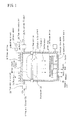
- Fig. 1 is a front view showing schematically an apparatus which realizes the process for producing a silicon compound according to the embodiment of the present invention. Prior to an explanation for the process according to the present embodiment, the apparatus will be described.
- a support base 2 is provided in the vicinity of the bottom of a chamber 1 formed in a cylindrical shape and made of, for example, a ceramic (made of an insulating material).
- a substrate 3 is placed on the support base 2.
- An interface of Si is exposed at the upper surface of the substrate 3.
- a temperature control means 6 equipped with a heater 4 and a coolant flow means 5 is provided in the support base 2.
- the support base 2 is controlled to a predetermined temperature (for example, a temperature at which the substrate 3 is maintained at 100 to 300°C) by the temperature control means 6.
- the upper surface of the chamber 1 is an opening portion, and the opening portion is closed with a ceiling plate 7 which is a plate of an insulating material (for example, a ceramic).
- a plasma antenna 8 for plasmatizing the interior of the chamber 1 is provided above the ceiling plate 7, and the plasma antenna 8 is formed in the shape of a flat ring parallel to the plane of the ceiling plate 7.
- a matching circuit 9 and a power supply 10 are connected to the plasma antenna 8 to supply a high frequency current.
- the plasma antenna 8, the matching circuit 9, and the power supply 10 constitute a plasma generation means for generating an inductive plasma.
- a member 11 to be etched which is formed of a material containing an element capable of forming a compound with Si, is held in the chamber 1.
- the member 11 to be etched is disposed in a discontinuous state, with respect to the flow of electricity of the plasma antenna 8, between the substrate 3 and the ceiling plate 7.
- the member 11 to be etched comprises rod-shaped protrusions 12 and a ring portion 13.
- the ring portion 13 is provided such that the protrusions 12 extend toward the center of the chamber 1. Because of this configuration, the member 11 to be etched is in a structurally discontinuous state with respect to a circumferential direction which is the direction of flow of electricity of the plasma antenna 8.
- a mode in which the member to be etched is formed like a lattice or like a network is conceivable as a configuration in which the member to be etched is brought into a discontinuous state with respect to the flow of electricity of the plasma antenna 8.
- Apluralityof nozzles 14 for supplying an acting gas (Cl 2 gas) 21 containing Cl as a halogen to the interior of the chamber 1 are connected (for example, at eight locations; two locations are shown in the drawing), with equal spacing in the circumferential direction, to the periphery of the tubular portion of the chamber 1 above the member 11 to be etched.
- Each of the nozzles 14 is fed with the Cl 2 gas 21 via a flow rate controller 15 which controls the flow rate and pressure.
- the flow rate controller 15 controls the amount of the Cl 2 gas 21 supplied into the chamber 1, thereby controlling a gas plasma density within the chamber 1.
- Substances such as a gas which does not take part in the reaction, are discharged through an exhaust port 18.
- the interior of the chamber 1 sealed by the ceiling plate 7 is maintained at a predetermined degree of vacuum by evacuation using a vacuum device 19.
- Fluorine, bromine and iodine can be applied as a halogen contained in the acting gas.
- an inexpensive Cl 2 gas is used as the halogen, whereby the running cost can be reduced.
- the Cl 2 gas 21 is supplied to the interior of the chamber 1 through the nozzles 14, and a high frequency electromagnetic wave is thrown by the plasma antenna 8 into the chamber 1. By so doing, the Cl 2 gas 21 is ionized to generate a Cl 2 gas plasma 23, generating Cl radicals.
- the gas plasma 23 acts on the member 11 to be etched, thereby heating the member 11 to be etched, and causing an etching reaction to the member 11 to be etched.
- a gaseous precursor 24 is formed which is a compound of the material for the member 11 to be etched and Cl.
- the precursor 24 is adsorbed onto the surface of the substrate 3 which is at a lower temperature than the temperature of the member 11 to be etched. Cl radicals act on the adsorbed precursor 24 to reduce it. As a result, a compound of Si with the material for the member 11 to be etched is produced on the substrate 3.
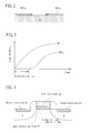
- NiSi can be produced on the substrate 3. If, during production of NiSi, a SiO 2 film and a Si interface are coexistent on the surface of the substrate 3, as shown in Fig. 2, a NiSi film is selectively formed at the Si interface. This is because the rate of formation of the NiSi film greatly differs, depending on whether the NiSi film is formed on Si or it is formed on SiO 2 . That is, as shown in Fig. 3, film formation on SiO 2 starts only after a lapse of a predetermined incubation time to, and the rate of film formation on SiO 2 is low after start of film formation.
- NiSi can be formed selectively only at the Si interface. Even if the Ni film is formed on SiO 2 the amount of its formation is very small compared with that of the NiSi film. Thus, the Ni film on SiO 2 can be removed easily.
- the desired silicon compound can be produced on the substrate 3 by selecting, as appropriate, the material for the member 11 to be etched.
- some methods for producing concrete silicon compounds will be described as working examples.
- This example is an example in which NiSi is produced as the source electrode 01 and the drain electrode 02 of the MOS transistor shown in Fig. 4.
- the substrate 3 in this case is in a state in which a SiO 2 film is formed on a Si substrate, and the SiO 2 film at sites where the source electrode 01 and the drain electrode 02 are to be formed is removed, with the Si interface being exposed at these sites.
- the substrate 3 of such a configuration is placed on the support base 2 within the chamber 1 of the apparatus shown in Fig. 1. At this time, the member 11 to be etched is formed of Ni.
- the Cl 2 gas 21 is supplied to the interior of the chamber 1 through the nozzles 14, and a high frequency electromagnetic wave is thrown by the plasma antenna 8 into the chamber 1.
- the Cl 2 gas 21 is ionized to generate the Cl 2 gas plasma 23 and generate Cl radicals.
- the following reactions are caused within the chamber 1, whereby the source electrode 01 and the drain electrode 02 each comprising the NiSi film at the Si interface can be formed.
- the above formula (1) shows a state in which Ni is etched with the gas plasma 23 (chlorine radicals Cl*) to form the precursor (NiCl) 24.
- the gas plasma 23 is generated to heat the member 11 to be etched (for example, at 300°C to 700°C), while the temperature of the substrate 3 is kept at a temperature lower than the temperature of the member 11 to be etched (for example, at a temperature of 100°C to 300°C) by the temperature control means 6.
- NiSi is produced by the following reducing action of chlorine radicals Cl*: NiCl (ad) + Cl* ⁇ NiSi (s) + Cl 2 ⁇ (3)
- the symbol s denotes a solid state
- g denotes a gaseous state
- ad denotes an adsorbed state
- This example is an example in which the gate electrode 03 of the MOS transistor shown in Fig. 4 is formed.
- the substrate 3 in this case is in a state in which a Si interface, such as polysilicon for formation of the gate electrode 03, is exposed.
- This substrate 3 is placed on the support base 2 within the chamber 1 of the apparatus shown in Fig. 1.
- the member 11 to be etched is formed of Ni.
- the Cl 2 gas 21 is supplied to the interior of the chamber 1 through the nozzles 14, and a high frequency electromagnetic wave is thrown by the plasma antenna 8 into the chamber 1.
- the Cl 2 gas 21 is ionized to generate the Cl 2 gas plasma 23 and generate Cl radicals.
- the following reactions are caused within the chamber 1, whereby the gate electrode 03 comprising a NiSi film at the Si interface can be formed.
- This example is an example in which the gate stack of the MOS transistor shown in Fig. 4 is formed.
- the SiO 2 film which is the gate insulating film 05 is formed on the n-type silicon substrate 04 as the substrate 3 in this case.
- a Ni film is formed on the gate insulating film 05 by the same method as in the above examples. By this measure, a part of the Si component of SiO 2 reacts with Ni to form a NiSi film as the gate electrode 03.
- All the electrodes 01, 02 and 03 of the MOS transistor can be formed by combining the first and second examples mentioned above.
- all the electrodes 01, 02 and 03 of the MOS transistor can be formed, and the entire gate structure including SiO 2 which is the gate insulating film 05, can be formed, by combining the first and third examples mentioned above.
- FeSi Among substances expected as materials for a solar cell is FeSi.
- FeSi it is necessary to form a p-type silicon layer and an n-type silicon layer of the solar cell from FeSi.
- the present invention can be applied, and shows excellent effects.
- the member 11 to be etched which is shown in Fig. 1, be formed of Fe, and an Fe film be formed on a p-type silicon layer or an n-type silicon layer of the substrate 3.
- Fe and Si react to formp-type and n-type FeSi layers, whereby the p-type layer and n-type layer of the solar cell can be formed.
- the apparatus shown in Fig. 1 can be utilized.
- the member 11 to be etched be formed of Si, and a p-type Si layer and an n-type Si layer be formed, with B being incorporated into a halogen gas as the acting gas, in the case of the p-type, or with p being incorporated into the halogen gas, in the case of the n-type.
- the member 11 to be etched which is formed of Si, can be omitted by incorporating Si into the acting gas.
- the mobility of an nMOS transistor can be increased by using SiC, instead of the conventional SiGe, as the source electrode 01 and the drain electrode 02 of the MOS transistor, thereby introducing tensile strain into the channel.
- SiC instead of the conventional SiGe, as the source electrode 01 and the drain electrode 02 of the MOS transistor, thereby introducing tensile strain into the channel.
- the application of the present invention obtains the aforementioned excellent effects. Concretely, it suffices to form the member 11 to be etched, shown in Fig. 1, from graphite, and perform the same steps as in the first example.
- the halogen gas is plasmatized within the chamber 1 to form its radicals.
- the method of radical formation need not be limited thereto.
- the radicals can be formed by any of the following methods:
Landscapes
- Chemical & Material Sciences (AREA)
- Organic Chemistry (AREA)
- General Chemical & Material Sciences (AREA)
- Mechanical Engineering (AREA)
- Engineering & Computer Science (AREA)
- Materials Engineering (AREA)
- Chemical Kinetics & Catalysis (AREA)
- Metallurgy (AREA)
- Inorganic Chemistry (AREA)
- Electrochemistry (AREA)
- Electrodes Of Semiconductors (AREA)
- Chemical Vapour Deposition (AREA)
- Insulated Gate Type Field-Effect Transistor (AREA)
Abstract
Description
- This invention relates to a process for producing a silicon compound, more particularly, that useful when applied in forming a metal silicide for use, for example, in an electrode of an MOS transistor.
- Fig. 4 is an explanation drawing showing an MOS transistor conceptually. As shown in this drawing, the MOS transistor has two p-regions formed on an n-
type silicon substrate 04, asource electrode 01 and adrain electrode 02 formed in the respective p-regions, and agate electrode 03 formed on the n-type silicon substrate 04 via a gateinsulating film 05 which is a SiO2 film. Such an MOS transistor having a NiSi film formed as thesource electrode 01, thedrain electrode 02 or thegate electrode 03 is produced. - In this case, heat treatment at 450°C is necessary for silicidization of Ni. However, Ni which has been deposited for the formation of NiSi, or an impurity with which a semiconductor has been doped, may be diffused to cause defects in device manufacturing, or deterioration of characteristics.
- To solve such problems, the following complicated process has been proposed: First, heat treatment at 400°C is performed to form a mixture of a nickel-rich silicide, such as Ni2Si, and Si at the desired site (gate electrode portion). Surplus Ni is removed by wet etching, and then heat treatment at 450°C is performed to form complete NiSi.
- Such a process involves the problems that the number of steps is large, and the treating temperature is still high. The higher the treating temperature, the more likely it is that problems will occur, such as the degradation of performance of the MOS transistor due to the diffusion of the doped impurity or the deterioration of insulation in the
gate insulating film 05. - The following are present as documents disclosing the above-described conventional technologies:
- Patent Document 1:
Japanese Unexamined Patent Publication No. 2005-019705
Patent Document 2:Japanese Unexamined Patent Publication No. 2004-165627
Patent Document 3:Japanese Patent Publication No. 1997-059013 - The present invention has been accomplished in the light of the above-described conventional technologies. It is an object of the invention to provide a process for producing a silicon compound which can minimize the number of steps and can form a desired compound in a low-temperature environment.
- A first aspect of the present invention, for solving the above problems, is a process for producing a silicon compound, comprising:
- allowing a radical of a halogen gas to act on a member to be etched, which is disposed within a chamber as a vacuum vessel and is formed of a material containing an element capable of forming a compound with Si, while keeping the member at a relatively high temperature, to form a gas of a precursor, which is a compound of the above material and the halogen;
- holding a substrate accommodated within the chamber at a relatively low temperature, with a Si interface of the substrate being exposed, to adsorb the precursor onto the Si interface of the substrate; and
- then allowing the radical of the halogen gas to act on the precursor adsorbed onto the Si interface to reduce the precursor, thereby producing a compound of the above material and Si.
- A second aspect of the present invention is the first aspect, characterized in that
the member to be etched is Ni, and
NiSi is produced at the Si interface. - A third aspect of the present invention is the first aspect, characterized in that
the member to be etched is Ni, and
an incubation time, which is a difference between times of production of a Ni compound of the precursor in a SiO2 region and a Si region, is utilized to produce NiSi only at the interface of the Si region of the substrate having a surface where the SiO2 region and the Si region are exposed and coexistent. - A fourth aspect of the present invention is any one of the first to third aspects, characterized in that
an electrode of an MOS transistor is formed from NiSi produced at the silicon interface. - A fifth aspect of the present invention is the first aspect, characterized in that
the member to be etched is graphite, and
an electrode of an MOS transistor is formed from SiC produced at the silicon interface. - A sixth aspect of the present invention is the first aspect, characterized in that
the member to be etched is Fe, and
a p-type layer or an n-type layer of a solar cell is formed from FeSi produced at the Si interface. - According to the present invention, a desired silicon compound is produced by a specific CVD apparatus which utilizes the etching reaction of the member to be etched, the adsorption reaction of the precursor formed by the etching reaction, and the reduction reaction of the adsorbed precursor. Thus, the silicon compound can be produced at a low temperature. Consequently, if a gate film or the like of a transistor is to be produced, in particular, a thin film of the desired silicon compound can be produced, with its characteristics free from deterioration. If a Si interface and SiO2 are coexistent, in particular, NiSi can be selectively grown at the Si interface. Thus, a source electrode and a drain electrode of an MOS transistor can be easily and efficiently formed.
- Furthermore, unlike the conventional technologies, there is no need for a separate step, such as removal of the unnecessary portion, after heat treatment is completed. Accordingly, the production of the compound concerned can be performed efficiently.
-
- [Fig. 1] is a front view schematically showing an apparatus for use in a process for producing a silicon compound according to an embodiment of the present invention.
- [Fig. 2] is an explanation drawing showing the coexistence of a Si interface and a SiO2 surface conceptually.
- [Fig. 3] is a graph showing the formation characteristics of a Ni film at the Si interface and the SiO2 surface.
- [Fig. 4] is an explanation drawing showing an MOS transistor conceptually.
-
- 1
- Chamber
- 3
- Substrate
- 8
- Plasma antenna
- 11
- Member to be etched
- 21
- Acting source
- An embodiment of the present invention will now be described in detail based on the accompanying drawings. The description of this embodiment is illustrative, and the features of the present invention are not limited to the following description.
- Fig. 1 is a front view showing schematically an apparatus which realizes the process for producing a silicon compound according to the embodiment of the present invention. Prior to an explanation for the process according to the present embodiment, the apparatus will be described.
- As shown in Fig. 1, a
support base 2 is provided in the vicinity of the bottom of achamber 1 formed in a cylindrical shape and made of, for example, a ceramic (made of an insulating material). Asubstrate 3 is placed on thesupport base 2. An interface of Si is exposed at the upper surface of thesubstrate 3. - A temperature control means 6 equipped with a
heater 4 and a coolant flow means 5 is provided in thesupport base 2. Thesupport base 2 is controlled to a predetermined temperature (for example, a temperature at which thesubstrate 3 is maintained at 100 to 300°C) by the temperature control means 6. - The upper surface of the
chamber 1 is an opening portion, and the opening portion is closed with aceiling plate 7 which is a plate of an insulating material (for example, a ceramic). Aplasma antenna 8 for plasmatizing the interior of thechamber 1 is provided above theceiling plate 7, and theplasma antenna 8 is formed in the shape of a flat ring parallel to the plane of theceiling plate 7. Amatching circuit 9 and apower supply 10 are connected to theplasma antenna 8 to supply a high frequency current. Theplasma antenna 8, thematching circuit 9, and thepower supply 10 constitute a plasma generation means for generating an inductive plasma. - A member 11 to be etched, which is formed of a material containing an element capable of forming a compound with Si, is held in the
chamber 1. The member 11 to be etched is disposed in a discontinuous state, with respect to the flow of electricity of theplasma antenna 8, between thesubstrate 3 and theceiling plate 7. For example, the member 11 to be etched comprises rod-shaped protrusions 12 and aring portion 13. Thering portion 13 is provided such that the protrusions 12 extend toward the center of thechamber 1. Because of this configuration, the member 11 to be etched is in a structurally discontinuous state with respect to a circumferential direction which is the direction of flow of electricity of theplasma antenna 8. - A mode in which the member to be etched is formed like a lattice or like a network is conceivable as a configuration in which the member to be etched is brought into a discontinuous state with respect to the flow of electricity of the
plasma antenna 8. -
Apluralityof nozzles 14 for supplying an acting gas (Cl2 gas) 21 containing Cl as a halogen to the interior of thechamber 1 are connected (for example, at eight locations; two locations are shown in the drawing), with equal spacing in the circumferential direction, to the periphery of the tubular portion of thechamber 1 above the member 11 to be etched. Each of thenozzles 14 is fed with the Cl2 gas 21 via aflow rate controller 15 which controls the flow rate and pressure. Theflow rate controller 15 controls the amount of the Cl2 gas 21 supplied into thechamber 1, thereby controlling a gas plasma density within thechamber 1. - Substances, such as a gas which does not take part in the reaction, are discharged through an
exhaust port 18. The interior of thechamber 1 sealed by theceiling plate 7 is maintained at a predetermined degree of vacuum by evacuation using avacuum device 19. - Fluorine, bromine and iodine can be applied as a halogen contained in the acting gas. In the present embodiment, an inexpensive Cl2 gas is used as the halogen, whereby the running cost can be reduced.
- To form a silicon compound on the
substrate 3 with the use of such an apparatus, the Cl2 gas 21 is supplied to the interior of thechamber 1 through thenozzles 14, and a high frequency electromagnetic wave is thrown by theplasma antenna 8 into thechamber 1. By so doing, the Cl2 gas 21 is ionized to generate a Cl2 gas plasma 23, generating Cl radicals. - Here, the
gas plasma 23 acts on the member 11 to be etched, thereby heating the member 11 to be etched, and causing an etching reaction to the member 11 to be etched. Upon this etching reaction, agaseous precursor 24 is formed which is a compound of the material for the member 11 to be etched and Cl. - The
precursor 24 is adsorbed onto the surface of thesubstrate 3 which is at a lower temperature than the temperature of the member 11 to be etched. Cl radicals act on the adsorbedprecursor 24 to reduce it. As a result, a compound of Si with the material for the member 11 to be etched is produced on thesubstrate 3. - If the member 11 to be etched is formed of Ni, NiSi can be produced on the
substrate 3. If, during production of NiSi, a SiO2 film and a Si interface are coexistent on the surface of thesubstrate 3, as shown in Fig. 2, a NiSi film is selectively formed at the Si interface. This is because the rate of formation of the NiSi film greatly differs, depending on whether the NiSi film is formed on Si or it is formed on SiO2. That is, as shown in Fig. 3, film formation on SiO2 starts only after a lapse of a predetermined incubation time to, and the rate of film formation on SiO2 is low after start of film formation. - If the incubation time t0 is utilized, and if it is attempted to complete film formation during this incubation time to, NiSi can be formed selectively only at the Si interface. Even if the Ni film is formed on SiO2 the amount of its formation is very small compared with that of the NiSi film. Thus, the Ni film on SiO2 can be removed easily.
- In the
substrate 3 where the Si interface and the SiO2 surface are coexistent, as noted above, selective growth of the NiSi film at the Si interface can be achieved. This is a major characteristic of the present invention. - According to the above-described embodiment, the desired silicon compound can be produced on the
substrate 3 by selecting, as appropriate, the material for the member 11 to be etched. Thus, some methods for producing concrete silicon compounds will be described as working examples. - This example is an example in which NiSi is produced as the
source electrode 01 and thedrain electrode 02 of the MOS transistor shown in Fig. 4. Thesubstrate 3 in this case is in a state in which a SiO2 film is formed on a Si substrate, and the SiO2 film at sites where thesource electrode 01 and thedrain electrode 02 are to be formed is removed, with the Si interface being exposed at these sites. Thesubstrate 3 of such a configuration is placed on thesupport base 2 within thechamber 1 of the apparatus shown in Fig. 1. At this time, the member 11 to be etched is formed of Ni. - Using such an apparatus, the Cl2 gas 21 is supplied to the interior of the
chamber 1 through thenozzles 14, and a high frequency electromagnetic wave is thrown by theplasma antenna 8 into thechamber 1. By so doing, the Cl2 gas 21 is ionized to generate the Cl2 gas plasma 23 and generate Cl radicals. As a result, the following reactions are caused within thechamber 1, whereby thesource electrode 01 and thedrain electrode 02 each comprising the NiSi film at the Si interface can be formed. - By the action of Cl* radicals, the following etching reaction of the member 11 to be etched proceeds:
Ni (s) + C1* → NiCl (g) (1)
- The above formula (1) shows a state in which Ni is etched with the gas plasma 23 (chlorine radicals Cl*) to form the precursor (NiCl) 24.
As noted above, thegas plasma 23 is generated to heat the member 11 to be etched (for example, at 300°C to 700°C), while the temperature of thesubstrate 3 is kept at a temperature lower than the temperature of the member 11 to be etched (for example, at a temperature of 100°C to 300°C) by the temperature control means 6. - Under the above temperature conditions, the following adsorption reaction of the
precursor 24 proceeds:
NiCl (g) → NiCl (ad) (2)
- NiSi is produced by the following reducing action of chlorine radicals Cl*:
NiCl (ad) + Cl* → NiSi (s) + Cl2↑ (3)
- In the above formulas (1) to (3), the symbol s denotes a solid state, g denotes a gaseous state, and ad denotes an adsorbed state.
- This example is an example in which the
gate electrode 03 of the MOS transistor shown in Fig. 4 is formed. Thesubstrate 3 in this case is in a state in which a Si interface, such as polysilicon for formation of thegate electrode 03, is exposed. Thissubstrate 3 is placed on thesupport base 2 within thechamber 1 of the apparatus shown in Fig. 1. At this time, the member 11 to be etched is formed of Ni. - Using such an apparatus, the Cl2 gas 21 is supplied to the interior of the
chamber 1 through thenozzles 14, and a high frequency electromagnetic wave is thrown by theplasma antenna 8 into thechamber 1. By so doing, the Cl2 gas 21 is ionized to generate the Cl2 gas plasma 23 and generate Cl radicals. As a result, the following reactions are caused within thechamber 1, whereby thegate electrode 03 comprising a NiSi film at the Si interface can be formed. - This example is an example in which the gate stack of the MOS transistor shown in Fig. 4 is formed. The SiO2 film which is the
gate insulating film 05 is formed on the n-type silicon substrate 04 as thesubstrate 3 in this case. A Ni film is formed on thegate insulating film 05 by the same method as in the above examples. By this measure, a part of the Si component of SiO2 reacts with Ni to form a NiSi film as thegate electrode 03. - All the
electrodes - Similarly, all the
electrodes gate insulating film 05, can be formed, by combining the first and third examples mentioned above. - Among substances expected as materials for a solar cell is FeSi. To prepare a solar cell by use of FeSi, it is necessary to form a p-type silicon layer and an n-type silicon layer of the solar cell from FeSi. In this case as well, the present invention can be applied, and shows excellent effects. Concretely, it is recommendable that the member 11 to be etched, which is shown in Fig. 1, be formed of Fe, and an Fe film be formed on a p-type silicon layer or an n-type silicon layer of the
substrate 3. By so doing, Fe and Si react to formp-type and n-type FeSi layers, whereby the p-type layer and n-type layer of the solar cell can be formed. - In forming the n-type silicon layer and the p-type silicon layer, the apparatus shown in Fig. 1 can be utilized. For example, it is advisable that the member 11 to be etched be formed of Si, and a p-type Si layer and an n-type Si layer be formed, with B being incorporated into a halogen gas as the acting gas, in the case of the p-type, or with p being incorporated into the halogen gas, in the case of the n-type.
- On this occasion, the member 11 to be etched, which is formed of Si, can be omitted by incorporating Si into the acting gas.
- Recently, it has been found that the mobility of an nMOS transistor can be increased by using SiC, instead of the conventional SiGe, as the
source electrode 01 and thedrain electrode 02 of the MOS transistor, thereby introducing tensile strain into the channel. In forming SiC in this case, the application of the present invention obtains the aforementioned excellent effects. Concretely, it suffices to form the member 11 to be etched, shown in Fig. 1, from graphite, and perform the same steps as in the first example. - In the apparatus shown in Fig. 1, the halogen gas is plasmatized within the
chamber 1 to form its radicals. However, the method of radical formation need not be limited thereto. For example, the radicals can be formed by any of the following methods: -
- 1) A high frequency electric field is allowed to act on a halogen gas flowing through a tubular passage communicating with the
chamber 1, to plasmatize the halogen gas. - 2) A microwave is supplied to a halogen gas flowing through a tubular passage communicating with the
chamber 1, to plasmatize the halogen gas. - 3) A halogen gas flowing through a tubular passage communicating with the
chamber 1 is heated for thermal dissociation. - 4) An electromagnetic wave or an electron beam is supplied to a halogen gas flowing through a tubular passage communicating with the
chamber 1, to dissociate the halogen gas. - 5) A halogen gas flowing through a tubular passage communicating with the
chamber 1 is brought into contact with a catalytic metal which dissociates the halogen gas by a catalytic action.
Claims (6)
- A process for producing a silicon compound, comprising:allowing a radical of a halogen gas to act on a member to be etched, which is disposed within a chamber as a vacuum vessel and is formed of a material containing an element capable of forming a compound with Si, while keeping the member at a relatively high temperature, to form a gas of a precursor, which is a compound of the material and the halogen;holding a substrate accommodated within the chamber at a relatively low temperature, with a Si interface of the substrate being exposed, to adsorb the precursor onto the Si interface of the substrate; andthen allowing the radical of the halogen gas to act on the precursor adsorbed onto the Si interface to reduce the precursor, thereby producing a compound of the material and Si.
- The process for producing a silicon compound according to claim 1, wherein
the member to be etched is Ni, and
NiSi is produced at the Si interface. - The process for producing a silicon compound according to claim 1, wherein
the member to be etched is Ni, and
an incubation time, which is a difference between times of production of a Ni compound of the precursor in a SiO2 region and a Si region, is utilized to produce NiSi only at the interface of the Si region of the substrate having a surface where the SiO2 region and the Si region are exposed and coexistent. - The process for producing a silicon compound according to any one of claims 1 to 3, wherein
an electrode of an MOS transistor is formed from NiSi produced at the silicon interface. - The process for producing a silicon compound according to claim 1, wherein
the member to be etched is graphite, and
an electrode of an MOS transistor is formed from SiC produced at the silicon interface. - The process for producing a silicon compound according to claim 1, wherein
the member to be etched is Fe, and
a p-type layer or an n-type layer of a solar cell is formed from FeSi produced at the Si interface.
Applications Claiming Priority (2)
| Application Number | Priority Date | Filing Date | Title |
|---|---|---|---|
| JP2005144616A JP4852261B2 (en) | 2005-05-17 | 2005-05-17 | Method for forming silicon compound |
| PCT/JP2006/309794 WO2006123673A1 (en) | 2005-05-17 | 2006-05-17 | Process for producing silicon compound |
Publications (2)
| Publication Number | Publication Date |
|---|---|
| EP1884987A1 true EP1884987A1 (en) | 2008-02-06 |
| EP1884987A4 EP1884987A4 (en) | 2012-11-21 |
Family
ID=37431245
Family Applications (1)
| Application Number | Title | Priority Date | Filing Date |
|---|---|---|---|
| EP06746497A Withdrawn EP1884987A4 (en) | 2005-05-17 | 2006-05-17 | PROCESS FOR PRODUCING A SILICON-BASED COMPOUND |
Country Status (5)
| Country | Link |
|---|---|
| US (1) | US7776751B2 (en) |
| EP (1) | EP1884987A4 (en) |
| JP (1) | JP4852261B2 (en) |
| KR (1) | KR100940824B1 (en) |
| WO (1) | WO2006123673A1 (en) |
Families Citing this family (2)
| Publication number | Priority date | Publication date | Assignee | Title |
|---|---|---|---|---|
| JPWO2008065908A1 (en) * | 2006-11-29 | 2010-03-04 | キヤノンアネルバ株式会社 | Method for forming metal group IV element compound film and method for manufacturing semiconductor device |
| US8617411B2 (en) * | 2011-07-20 | 2013-12-31 | Lam Research Corporation | Methods and apparatus for atomic layer etching |
Family Cites Families (16)
| Publication number | Priority date | Publication date | Assignee | Title |
|---|---|---|---|---|
| JP3194256B2 (en) | 1991-11-14 | 2001-07-30 | 富士通株式会社 | Film growth method and film growth apparatus |
| JP3084497B2 (en) * | 1992-03-25 | 2000-09-04 | 東京エレクトロン株式会社 | Method for etching SiO2 film |
| JPH06318563A (en) * | 1993-05-10 | 1994-11-15 | Toshiba Corp | Semiconductor device and manufacturing method thereof |
| JPH0794446A (en) * | 1993-09-20 | 1995-04-07 | Hitachi Ltd | Method for manufacturing semiconductor device |
| JPH0959013A (en) | 1995-08-22 | 1997-03-04 | Mitsubishi Heavy Ind Ltd | Preparation of silicide film |
| JP2001024194A (en) | 1999-05-06 | 2001-01-26 | Toshiba Corp | Semiconductor device manufacturing method and semiconductor device |
| JP2001064099A (en) | 1999-08-26 | 2001-03-13 | Matsushita Electronics Industry Corp | Thin film formation |
| JP3727878B2 (en) * | 2001-11-14 | 2005-12-21 | 三菱重工業株式会社 | Metal film production equipment |
| JP3716235B2 (en) | 2002-03-08 | 2005-11-16 | 三菱重工業株式会社 | Metal film manufacturing method and metal film manufacturing apparatus |
| DE60329292D1 (en) * | 2002-03-08 | 2009-10-29 | Canon Anelva Corp | Method and device for producing metal layers |
| JP3733424B2 (en) * | 2002-07-08 | 2006-01-11 | 国立大学法人名古屋大学 | Nickel-silicon thin film, nickel-silicon multilayer structure, and method for producing nickel-silicon thin film |
| JP3782763B2 (en) * | 2002-08-23 | 2006-06-07 | 三菱重工業株式会社 | Metal film manufacturing method and metal film manufacturing apparatus |
| KR100446309B1 (en) | 2002-11-14 | 2004-09-01 | 삼성전자주식회사 | Method of fabricating semiconductor device having L-type spacer |
| JP3840198B2 (en) * | 2003-04-28 | 2006-11-01 | 株式会社東芝 | Semiconductor device and manufacturing method thereof |
| JP3872773B2 (en) * | 2003-06-25 | 2007-01-24 | 三菱重工業株式会社 | Metal film manufacturing method and metal film manufacturing apparatus |
| JP3828511B2 (en) * | 2003-06-26 | 2006-10-04 | 株式会社東芝 | Manufacturing method of semiconductor device |
-
2005
- 2005-05-17 JP JP2005144616A patent/JP4852261B2/en not_active Expired - Fee Related
-
2006
- 2006-05-17 KR KR1020077029289A patent/KR100940824B1/en not_active Expired - Fee Related
- 2006-05-17 WO PCT/JP2006/309794 patent/WO2006123673A1/en not_active Ceased
- 2006-05-17 US US11/919,484 patent/US7776751B2/en not_active Expired - Fee Related
- 2006-05-17 EP EP06746497A patent/EP1884987A4/en not_active Withdrawn
Also Published As
| Publication number | Publication date |
|---|---|
| KR20080017364A (en) | 2008-02-26 |
| WO2006123673A1 (en) | 2006-11-23 |
| US20090081869A1 (en) | 2009-03-26 |
| KR100940824B1 (en) | 2010-02-05 |
| JP4852261B2 (en) | 2012-01-11 |
| US7776751B2 (en) | 2010-08-17 |
| EP1884987A4 (en) | 2012-11-21 |
| JP2006324357A (en) | 2006-11-30 |
Similar Documents
| Publication | Publication Date | Title |
|---|---|---|
| KR102554853B1 (en) | Method for fabricating junctions and spacers for horizontal gate all around devices | |
| US7759598B2 (en) | Substrate treating method and production method for semiconductor device | |
| KR101189926B1 (en) | Plasma cvd method, method for forming silicon nitride film and method for manufacturing semiconductor device | |
| JP5283147B2 (en) | Semiconductor device and manufacturing method of semiconductor device | |
| JP2006261217A (en) | Thin film formation method | |
| KR20110104001A (en) | Method and apparatus for growing oxide thin films on silicon with minimal effect on existing structures | |
| WO2016111833A1 (en) | Direct deposition of nickel silicide nanowire | |
| CN117637438A (en) | Adding Argon to Remote Plasma Oxidation | |
| US20130023111A1 (en) | Low temperature methods and apparatus for microwave crystal regrowth | |
| JP2004533727A (en) | Method for increasing mobility of inversion layer of silicon carbide metal oxide semiconductor field effect transistor | |
| JP5018473B2 (en) | Manufacturing method of semiconductor device | |
| JP2008282921A (en) | Method for introducing dopant element into silicon layer, method for producing polysilicon solar cell, method for producing polysilicon thin film transistor, and apparatus for introducing dopant element into silicon layer | |
| JP7400389B2 (en) | Silicon carbide polycrystalline film, silicon carbide polycrystalline film manufacturing method, and silicon carbide polycrystalline film forming apparatus | |
| KR20230149249A (en) | Contact formation process for cmos devices | |
| US7776751B2 (en) | Process for producing silicon compound | |
| JP5618430B2 (en) | Semiconductor device and manufacturing method thereof | |
| CN116261774A (en) | Growth of thin oxide layers utilizing amorphous silicon and oxidation | |
| CN117238758A (en) | Method for passivating SiC MOS interface defects by sacrificial oxidation NANO-P doping EPI | |
| CN117219674A (en) | A kind of superjunction trench type MOSFET device and preparation method | |
| TWI520335B (en) | Method and apparatus for forming a semiconductor structure | |
| JP2006319306A (en) | In situ growth method for polycrystalline thin films. | |
| CN117497605A (en) | PMOS with low on-resistance at high temperature and preparation method thereof | |
| Liao et al. | NMOS SiP Epitaxy Process-Optimizing Facet Growth | |
| KR100368318B1 (en) | Method of processing for selective epitaxial growth in semiconductor device | |
| CN117497604A (en) | Improved planar gate MOSFET and preparation method |
Legal Events
| Date | Code | Title | Description |
|---|---|---|---|
| PUAI | Public reference made under article 153(3) epc to a published international application that has entered the european phase |
Free format text: ORIGINAL CODE: 0009012 |
|
| 17P | Request for examination filed |
Effective date: 20071120 |
|
| AK | Designated contracting states |
Kind code of ref document: A1 Designated state(s): AT BE BG CH CY CZ DE DK EE ES FI FR GB GR HU IE IS IT LI LT LU LV MC NL PL PT RO SE SI SK TR |
|
| DAX | Request for extension of the european patent (deleted) | ||
| RAP1 | Party data changed (applicant data changed or rights of an application transferred) |
Owner name: CANON ANELVA CORPORATION |
|
| A4 | Supplementary search report drawn up and despatched |
Effective date: 20121024 |
|
| RIC1 | Information provided on ipc code assigned before grant |
Ipc: C23C 16/44 20060101ALI20121019BHEP Ipc: H01L 21/28 20060101ALI20121019BHEP Ipc: C23C 16/32 20060101ALI20121019BHEP Ipc: H01L 21/336 20060101ALI20121019BHEP Ipc: C23C 16/42 20060101ALI20121019BHEP Ipc: C01B 33/06 20060101ALI20121019BHEP Ipc: H01L 21/285 20060101AFI20121019BHEP Ipc: H01L 31/04 20060101ALI20121019BHEP Ipc: H01L 29/78 20060101ALI20121019BHEP |
|
| STAA | Information on the status of an ep patent application or granted ep patent |
Free format text: STATUS: THE APPLICATION HAS BEEN WITHDRAWN |
|
| 18W | Application withdrawn |
Effective date: 20130502 |