EP1881530A1 - Power semiconductor apparatus - Google Patents
Power semiconductor apparatus Download PDFInfo
- Publication number
- EP1881530A1 EP1881530A1 EP06026107A EP06026107A EP1881530A1 EP 1881530 A1 EP1881530 A1 EP 1881530A1 EP 06026107 A EP06026107 A EP 06026107A EP 06026107 A EP06026107 A EP 06026107A EP 1881530 A1 EP1881530 A1 EP 1881530A1
- Authority
- EP
- European Patent Office
- Prior art keywords
- case
- resin package
- power semiconductor
- semiconductor element
- power
- Prior art date
- Legal status (The legal status is an assumption and is not a legal conclusion. Google has not performed a legal analysis and makes no representation as to the accuracy of the status listed.)
- Granted
Links
Images

Classifications
-
- H—ELECTRICITY
- H10—SEMICONDUCTOR DEVICES; ELECTRIC SOLID-STATE DEVICES NOT OTHERWISE PROVIDED FOR
- H10W—GENERIC PACKAGES, INTERCONNECTIONS, CONNECTORS OR OTHER CONSTRUCTIONAL DETAILS OF DEVICES COVERED BY CLASS H10
- H10W90/00—Package configurations
-
- H—ELECTRICITY
- H10—SEMICONDUCTOR DEVICES; ELECTRIC SOLID-STATE DEVICES NOT OTHERWISE PROVIDED FOR
- H10W—GENERIC PACKAGES, INTERCONNECTIONS, CONNECTORS OR OTHER CONSTRUCTIONAL DETAILS OF DEVICES COVERED BY CLASS H10
- H10W40/00—Arrangements for thermal protection or thermal control
- H10W40/10—Arrangements for heating
-
- H—ELECTRICITY
- H10—SEMICONDUCTOR DEVICES; ELECTRIC SOLID-STATE DEVICES NOT OTHERWISE PROVIDED FOR
- H10W—GENERIC PACKAGES, INTERCONNECTIONS, CONNECTORS OR OTHER CONSTRUCTIONAL DETAILS OF DEVICES COVERED BY CLASS H10
- H10W42/00—Arrangements for protection of devices
- H10W42/121—Arrangements for protection of devices protecting against mechanical damage
-
- H—ELECTRICITY
- H10—SEMICONDUCTOR DEVICES; ELECTRIC SOLID-STATE DEVICES NOT OTHERWISE PROVIDED FOR
- H10W—GENERIC PACKAGES, INTERCONNECTIONS, CONNECTORS OR OTHER CONSTRUCTIONAL DETAILS OF DEVICES COVERED BY CLASS H10
- H10W72/00—Interconnections or connectors in packages
- H10W72/071—Connecting or disconnecting
- H10W72/076—Connecting or disconnecting of strap connectors
- H10W72/07651—Connecting or disconnecting of strap connectors characterised by changes in properties of the strap connectors during connecting
- H10W72/07653—Connecting or disconnecting of strap connectors characterised by changes in properties of the strap connectors during connecting changes in shapes
-
- H—ELECTRICITY
- H10—SEMICONDUCTOR DEVICES; ELECTRIC SOLID-STATE DEVICES NOT OTHERWISE PROVIDED FOR
- H10W—GENERIC PACKAGES, INTERCONNECTIONS, CONNECTORS OR OTHER CONSTRUCTIONAL DETAILS OF DEVICES COVERED BY CLASS H10
- H10W72/00—Interconnections or connectors in packages
- H10W72/50—Bond wires
- H10W72/551—Materials of bond wires
- H10W72/552—Materials of bond wires comprising metals or metalloids, e.g. silver
- H10W72/5524—Materials of bond wires comprising metals or metalloids, e.g. silver comprising aluminium [Al]
-
- H—ELECTRICITY
- H10—SEMICONDUCTOR DEVICES; ELECTRIC SOLID-STATE DEVICES NOT OTHERWISE PROVIDED FOR
- H10W—GENERIC PACKAGES, INTERCONNECTIONS, CONNECTORS OR OTHER CONSTRUCTIONAL DETAILS OF DEVICES COVERED BY CLASS H10
- H10W72/00—Interconnections or connectors in packages
- H10W72/60—Strap connectors, e.g. thick copper clips for grounding of power devices
- H10W72/651—Materials of strap connectors
- H10W72/652—Materials of strap connectors comprising metals or metalloids, e.g. silver
-
- H—ELECTRICITY
- H10—SEMICONDUCTOR DEVICES; ELECTRIC SOLID-STATE DEVICES NOT OTHERWISE PROVIDED FOR
- H10W—GENERIC PACKAGES, INTERCONNECTIONS, CONNECTORS OR OTHER CONSTRUCTIONAL DETAILS OF DEVICES COVERED BY CLASS H10
- H10W72/00—Interconnections or connectors in packages
- H10W72/851—Dispositions of multiple connectors or interconnections
- H10W72/853—On the same surface
- H10W72/871—Bond wires and strap connectors
-
- H—ELECTRICITY
- H10—SEMICONDUCTOR DEVICES; ELECTRIC SOLID-STATE DEVICES NOT OTHERWISE PROVIDED FOR
- H10W—GENERIC PACKAGES, INTERCONNECTIONS, CONNECTORS OR OTHER CONSTRUCTIONAL DETAILS OF DEVICES COVERED BY CLASS H10
- H10W72/00—Interconnections or connectors in packages
- H10W72/851—Dispositions of multiple connectors or interconnections
- H10W72/874—On different surfaces
- H10W72/884—Die-attach connectors and bond wires
-
- H—ELECTRICITY
- H10—SEMICONDUCTOR DEVICES; ELECTRIC SOLID-STATE DEVICES NOT OTHERWISE PROVIDED FOR
- H10W—GENERIC PACKAGES, INTERCONNECTIONS, CONNECTORS OR OTHER CONSTRUCTIONAL DETAILS OF DEVICES COVERED BY CLASS H10
- H10W72/00—Interconnections or connectors in packages
- H10W72/851—Dispositions of multiple connectors or interconnections
- H10W72/874—On different surfaces
- H10W72/886—Die-attach connectors and strap connectors
-
- H—ELECTRICITY
- H10—SEMICONDUCTOR DEVICES; ELECTRIC SOLID-STATE DEVICES NOT OTHERWISE PROVIDED FOR
- H10W—GENERIC PACKAGES, INTERCONNECTIONS, CONNECTORS OR OTHER CONSTRUCTIONAL DETAILS OF DEVICES COVERED BY CLASS H10
- H10W74/00—Encapsulations, e.g. protective coatings
-
- H—ELECTRICITY
- H10—SEMICONDUCTOR DEVICES; ELECTRIC SOLID-STATE DEVICES NOT OTHERWISE PROVIDED FOR
- H10W—GENERIC PACKAGES, INTERCONNECTIONS, CONNECTORS OR OTHER CONSTRUCTIONAL DETAILS OF DEVICES COVERED BY CLASS H10
- H10W90/00—Package configurations
- H10W90/701—Package configurations characterised by the relative positions of pads or connectors relative to package parts
- H10W90/751—Package configurations characterised by the relative positions of pads or connectors relative to package parts of bond wires
- H10W90/756—Package configurations characterised by the relative positions of pads or connectors relative to package parts of bond wires between a chip and a stacked lead frame, conducting package substrate or heat sink
-
- H—ELECTRICITY
- H10—SEMICONDUCTOR DEVICES; ELECTRIC SOLID-STATE DEVICES NOT OTHERWISE PROVIDED FOR
- H10W—GENERIC PACKAGES, INTERCONNECTIONS, CONNECTORS OR OTHER CONSTRUCTIONAL DETAILS OF DEVICES COVERED BY CLASS H10
- H10W90/00—Package configurations
- H10W90/701—Package configurations characterised by the relative positions of pads or connectors relative to package parts
- H10W90/761—Package configurations characterised by the relative positions of pads or connectors relative to package parts of strap connectors
- H10W90/766—Package configurations characterised by the relative positions of pads or connectors relative to package parts of strap connectors between a chip and a stacked lead frame, conducting package substrate or heat sink
Definitions
- the present invention relates to a case type power semiconductor apparatus which encloses a power semiconductor element and a control semiconductor element with a case, and more particularly, to a power semiconductor apparatus providing excellent productivity and moreover excellent recyclability which facilitates reuse of the case.
- IPM Insulated Gate Bipolar Transistor
- a mold type IPM is used for consumer applications.
- This mold type IPM is made up of an IC and a power semiconductor chip (IGBT, diode) which are die-mounted on a Cu frame and consolidated with epoxy mold resin.
- IGBT power semiconductor chip
- There is also a proposal of a mold type IPM provided with a heat sink to improve a heat radiation characteristic for example, see Japanese Patent Laid-Open No. 2001-085613 ).
- a case type IPM is used as a small/medium capacity industrial IPM (600 V/50 A or above).
- Fig. 3 is a sectional view showing a conventional case type IPM and
- Fig. 4 is a top view thereof.
- An insertion case 1 incorporates an insulating substrate 4 mounted with an IGBT chip 2 and a diode 3 as power semiconductor elements and a mounting substrate 5 mounted with a control IC as a control semiconductor element, resistors and capacitors. These components are connected to each other using A1 wires 6.
- the IGBT chip 2 and diode 3 are connected to the outside through a power terminal 7 incorporated in the insertion case
- the case type IPM includes more parts and requires higher assembly cost, and is therefore inferior in productivity. Furthermore, as in the case of the mold type IPM, the case type IPM involves a problem that when the case is filled with resin, the case cannot be reused.
- the present invention has been implemented to solve the above described problems and it is an object of the present invention to provide a case type power semiconductor apparatus providing excellent productivity and excellent recyclability facilitating reuse of the case.
- the power semiconductor apparatus includes a resin package made up of a power semiconductor element and a control semiconductor element which are mounted on a main front surface of a lead frame and sealed with mold resin, a power terminal led out of the resin package and electrically connected to the power semiconductor element, a control terminal led out of the resin package and electrically connected to the control semiconductor element and a cylindrical case which is formed in a manner separable from the resin package and encloses the resin package, wherein the power terminal and the control terminal are led out of lead insertion slots formed in the case, and a part of the power terminal which is led out of the case is bent along an end face of the case.
- the present invention makes it possible to realize a case type power semiconductor apparatus providing excellent productivity and excellent recyclability facilitating reuse of the case.
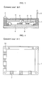
- Fig. 1 is a sectional view showing a power semiconductor apparatus according to Embodiment 1 of the present invention.
- a power semiconductor element 12 such as an IGBT chip and diode and a control semiconductor element 13 such as a control IC are mounted on the main front surface of lead frames 11. These components are electrically connected to each other through A1 wires 14. Furthermore, the power semiconductor element 12 is electrically connected to a power terminal 16 through a Cu terminal 15 and the control semiconductor element 13 is electrically connected to a control terminal 17 through an A1 wire 14.
- a heat sink 19 is provided through an insulation sheet 18 on the main back surface of the lead frame 11.
- a resin package 21 is formed by sealing these components with mold resin 20. Furthermore, the power terminal 16 and control terminal 17 are led out of the resin package 21. A part of the outside surface of the heat sink 19 is exposed from the resin package 21.
- the heat radiation characteristic of the resin package 21 can be improved by this heat sink 19. More specifically, the heat resistance is 0.6°C/W at 600 V/50 A and it is possible to achieve heat resistance substantially equivalent to that of the conventional case type IPM.
- the heat sink 19 requires no fixing means.
- the resin package 21 is enclosed by a cylindrical insertion case 22 made of plastic.
- the power terminal 16 and control terminal 17 are led out of lead insertion slots 23 which are provided in the insertion case 22.
- the part of the power terminal 16 which is led out of the insertion case 22 is bent along the end face of the insertion case 22.
- An outside wire (not shown) is made to contact the bent part of this power terminal 16 and the two parts are connected with a screw which penetrates the two parts.
- the power semiconductor apparatus has the same locations of the power terminal and the control terminal as the conventional case type IPM in appearance, which allows the customer to handle the apparatus using the same assembly method as that for the conventional case type IPM and eliminates the necessity for modifying the apparatus.
- the insertion case 22 is made separable from the resin package 21. In this way, when the power semiconductor element 12 and the control semiconductor element 13 or the like are damaged, only the resin package 21 can be replaced. Therefore, it is possible to realize a power semiconductor apparatus providing excellent recyclability which makes reuse of the case easier.
- peripheral edges of the heat sink 19 protrude from peripheral edges of an enclosure of the resin package 21 and are engaged with open end edges of the insertion case 22. This eliminates the necessity for fixing means for fixing the resin package 21 to the insertion case 22, and can thereby provide a power semiconductor apparatus providing excellent assemblability, that is, excellent productivity.
- Fig. 2 is a sectional view showing a power semiconductor apparatus according to Embodiment 2 of the present invention.
- peripheral edges of a heat sink 19 protrude from peripheral edges of an enclosure of a resin package 21 and are connected to open end edges of an insertion case 22 using bolts 24.
- the rest of the configuration is the same as that of Embodiment 1.
Landscapes
- Structures Or Materials For Encapsulating Or Coating Semiconductor Devices Or Solid State Devices (AREA)
- Cooling Or The Like Of Semiconductors Or Solid State Devices (AREA)
- Inverter Devices (AREA)
Abstract
Description
- The present invention relates to a case type power semiconductor apparatus which encloses a power semiconductor element and a control semiconductor element with a case, and more particularly, to a power semiconductor apparatus providing excellent productivity and moreover excellent recyclability which facilitates reuse of the case.
- In recent years, there is a growing demand for IPM modularization of an IGBT module (Insulated Gate Bipolar Transistor) used for industrial motor control and servo applications. Here, "IPM" is a power module which incorporates a drive circuit and a self protection function for a power device such as a MOSFET and IGBT which controls power.
- A mold type IPM is used for consumer applications. This mold type IPM is made up of an IC and a power semiconductor chip (IGBT, diode) which are die-mounted on a Cu frame and consolidated with epoxy mold resin. There is also a proposal of a mold type IPM provided with a heat sink to improve a heat radiation characteristic (for example, see
Japanese Patent Laid-Open No. 2001-085613 - On the other hand, a case type IPM is used as a small/medium capacity industrial IPM (600 V/50 A or above). Fig. 3 is a sectional view showing a conventional case type IPM and Fig. 4 is a top view thereof. An
insertion case 1 incorporates an insulating substrate 4 mounted with anIGBT chip 2 and adiode 3 as power semiconductor elements and amounting substrate 5 mounted with a control IC as a control semiconductor element, resistors and capacitors. These components are connected to each other usingA1 wires 6. - Furthermore, the
IGBT chip 2 anddiode 3 are connected to the outside through apower terminal 7 incorporated in the insertion case - 1. The
mounting substrate 5 is connected to the outside through a control terminal 8 incorporated in theinsertion case 1. Furthermore, aCu base 9 is formed on the back side of the insulating substrate 4 to radiate heat from theIGBT chip 2 anddiode 3. Moreover,case rings 10 are provided in the four corners of theinsertion case 1. - However, compared to the mold type IPM, the case type IPM includes more parts and requires higher assembly cost, and is therefore inferior in productivity. Furthermore, as in the case of the mold type IPM, the case type IPM involves a problem that when the case is filled with resin, the case cannot be reused.
- The present invention has been implemented to solve the above described problems and it is an object of the present invention to provide a case type power semiconductor apparatus providing excellent productivity and excellent recyclability facilitating reuse of the case.
- According to one aspect of the present invention, the power semiconductor apparatus includes a resin package made up of a power semiconductor element and a control semiconductor element which are mounted on a main front surface of a lead frame and sealed with mold resin, a power terminal led out of the resin package and electrically connected to the power semiconductor element, a control terminal led out of the resin package and electrically connected to the control semiconductor element and a cylindrical case which is formed in a manner separable from the resin package and encloses the resin package, wherein the power terminal and the control terminal are led out of lead insertion slots formed in the case, and a part of the power terminal which is led out of the case is bent along an end face of the case.
- The present invention makes it possible to realize a case type power semiconductor apparatus providing excellent productivity and excellent recyclability facilitating reuse of the case.
- Other and further objects, features and advantages of the invention will appear more fully from the following description.
-
- Fig. 1 is a sectional view showing a power semiconductor apparatus according to
Embodiment 1 of the present invention. - Fig. 2 is a sectional view showing a power semiconductor apparatus according to
Embodiment 2 of the present invention. - Fig. 3 is a sectional view showing a conventional case type IPM.
- Fig. 4 is a top view showing a conventional case type IPM.
- Fig. 1 is a sectional view showing a power semiconductor apparatus according to
Embodiment 1 of the present invention. Apower semiconductor element 12 such as an IGBT chip and diode and acontrol semiconductor element 13 such as a control IC are mounted on the main front surface oflead frames 11. These components are electrically connected to each other throughA1 wires 14. Furthermore, thepower semiconductor element 12 is electrically connected to apower terminal 16 through aCu terminal 15 and thecontrol semiconductor element 13 is electrically connected to acontrol terminal 17 through anA1 wire 14. - A
heat sink 19 is provided through aninsulation sheet 18 on the main back surface of thelead frame 11. Aresin package 21 is formed by sealing these components withmold resin 20. Furthermore, thepower terminal 16 andcontrol terminal 17 are led out of theresin package 21. A part of the outside surface of theheat sink 19 is exposed from theresin package 21. The heat radiation characteristic of theresin package 21 can be improved by thisheat sink 19. More specifically, the heat resistance is 0.6°C/W at 600 V/50 A and it is possible to achieve heat resistance substantially equivalent to that of the conventional case type IPM. Theheat sink 19 requires no fixing means. - The
resin package 21 is enclosed by acylindrical insertion case 22 made of plastic. Thepower terminal 16 andcontrol terminal 17 are led out oflead insertion slots 23 which are provided in theinsertion case 22. Moreover, the part of thepower terminal 16 which is led out of theinsertion case 22 is bent along the end face of theinsertion case 22. An outside wire (not shown) is made to contact the bent part of thispower terminal 16 and the two parts are connected with a screw which penetrates the two parts. - As explained above, partially adopting a mold type IPM structure makes it possible to reduce assembly parts and reduce cost compared to the conventional case type IPM and realize a power semiconductor apparatus providing excellent productivity. Moreover, the power semiconductor apparatus according to this embodiment has the same locations of the power terminal and the control terminal as the conventional case type IPM in appearance, which allows the customer to handle the apparatus using the same assembly method as that for the conventional case type IPM and eliminates the necessity for modifying the apparatus.
- Furthermore, by avoiding the
mold resin 20 from filling theinsertion case 22, theinsertion case 22 is made separable from theresin package 21. In this way, when thepower semiconductor element 12 and thecontrol semiconductor element 13 or the like are damaged, only theresin package 21 can be replaced. Therefore, it is possible to realize a power semiconductor apparatus providing excellent recyclability which makes reuse of the case easier. - Furthermore, peripheral edges of the
heat sink 19 protrude from peripheral edges of an enclosure of theresin package 21 and are engaged with open end edges of theinsertion case 22. This eliminates the necessity for fixing means for fixing theresin package 21 to theinsertion case 22, and can thereby provide a power semiconductor apparatus providing excellent assemblability, that is, excellent productivity. - Fig. 2 is a sectional view showing a power semiconductor apparatus according to
Embodiment 2 of the present invention. In this embodiment, peripheral edges of aheat sink 19 protrude from peripheral edges of an enclosure of aresin package 21 and are connected to open end edges of aninsertion case 22 usingbolts 24. The rest of the configuration is the same as that ofEmbodiment 1. - In this way, it is possible to reduce the number of parts and provide a power semiconductor apparatus with excellent assemblability, that is, excellent productivity. Furthermore, the strength of mounting the resin package and the case is greater than that of
Embodiment 1. - Obviously many modifications and variations of the present invention are possible in the light of the above teachings. It is therefore to be understood that within the scope of the appended claims the invention may be practiced otherwise than as specif ically described.
- The entire disclosure of a
Japanese Patent Application No. 2006-196259, filed on July 18, 2006
Claims (4)
- A power semiconductor apparatus comprising:a resin package made up of a power semiconductor element (12) and a control semiconductor element (13) which are mounted on a main front surface of a lead frame (11) and sealed with mold resin;a power terminal (16) led out of said resin package and electrically connected to said power semiconductor element (12);a control terminal (17) led out of said resin package and electrically connected to said control semiconductor element (13); anda cylindrical case (22) which is formed in a manner separable from said resin package and encloses said resin package,wherein said power terminal (16) and said control terminal (17) are led out of lead insertion slots (23) formed in said case, anda part of said power terminal which is led out of said case is bent along an end face of said case.
- The power semiconductor apparatus according to claim 1, wherein said resin package further comprises a heat sink (19) provided on a main back surface of said lead frame and a part of an outside surface is exposed from said resin package.
- The power semiconductor apparatus according to claim 2, wherein the peripheral edges of said heat sink (19) protrude from peripheral edges of an enclosure of said resin package and are engaged with open end edges of said case.
- The power semiconductor apparatus according to claim 2 or 3, wherein the peripheral edges of said heat sink (19) protrude from peripheral edges of an enclosure of said resin package and are connected to open end edges of said case bolts (24).
Applications Claiming Priority (1)
| Application Number | Priority Date | Filing Date | Title |
|---|---|---|---|
| JP2006196259A JP4760585B2 (en) | 2006-07-18 | 2006-07-18 | Power semiconductor device |
Publications (2)
| Publication Number | Publication Date |
|---|---|
| EP1881530A1 true EP1881530A1 (en) | 2008-01-23 |
| EP1881530B1 EP1881530B1 (en) | 2016-03-16 |
Family
ID=38259385
Family Applications (1)
| Application Number | Title | Priority Date | Filing Date |
|---|---|---|---|
| EP06026107.0A Active EP1881530B1 (en) | 2006-07-18 | 2006-12-15 | Power semiconductor apparatus |
Country Status (5)
| Country | Link |
|---|---|
| US (1) | US7449726B2 (en) |
| EP (1) | EP1881530B1 (en) |
| JP (1) | JP4760585B2 (en) |
| KR (1) | KR100898774B1 (en) |
| TW (1) | TWI334216B (en) |
Cited By (1)
| Publication number | Priority date | Publication date | Assignee | Title |
|---|---|---|---|---|
| JP2013051300A (en) * | 2011-08-31 | 2013-03-14 | Sanken Electric Co Ltd | Semiconductor module |
Families Citing this family (35)
| Publication number | Priority date | Publication date | Assignee | Title |
|---|---|---|---|---|
| KR101221807B1 (en) * | 2006-12-29 | 2013-01-14 | 페어차일드코리아반도체 주식회사 | Power device package |
| CN201011655Y (en) * | 2007-01-10 | 2008-01-23 | 上海凯虹科技电子有限公司 | A frame of a high-power semiconductor device |
| JP5112101B2 (en) * | 2007-02-15 | 2013-01-09 | 株式会社東芝 | Semiconductor package |
| CN101681905B (en) * | 2007-05-18 | 2012-06-13 | 株式会社三社电机制作所 | Arc discharge device |
| CN101681907B (en) * | 2007-11-30 | 2012-11-07 | 松下电器产业株式会社 | Heat dissipating structure base board, module using heat dissipating structure base board, and method for manufacturing heat dissipating structure base board |
| KR101454321B1 (en) * | 2008-01-22 | 2014-10-23 | 페어차일드코리아반도체 주식회사 | Semiconductor package with insulated metal substrate and method of fabricating the same |
| DE102008031231B4 (en) * | 2008-07-02 | 2012-12-27 | Siemens Aktiengesellschaft | Manufacturing process for planar electronic power electronics modules for high-temperature applications and corresponding power electronics module |
| TW201011869A (en) * | 2008-09-10 | 2010-03-16 | Cyntec Co Ltd | Chip package structure |
| US8076696B2 (en) * | 2009-10-30 | 2011-12-13 | General Electric Company | Power module assembly with reduced inductance |
| CN101834267B (en) * | 2010-04-30 | 2013-07-10 | 深圳市奥伦德元器件有限公司 | Planar bracket and encapsulating method |
| CN102340233B (en) * | 2010-07-15 | 2014-05-07 | 台达电子工业股份有限公司 | Power module |
| JP2013016629A (en) * | 2011-07-04 | 2013-01-24 | Mitsubishi Electric Corp | Semiconductor module |
| US9147637B2 (en) * | 2011-12-23 | 2015-09-29 | Infineon Technologies Ag | Module including a discrete device mounted on a DCB substrate |
| CN103430307B (en) * | 2012-02-13 | 2016-04-27 | 松下知识产权经营株式会社 | Semiconductor device and manufacture method thereof |
| JP5796640B2 (en) | 2012-02-14 | 2015-10-21 | 三菱電機株式会社 | Semiconductor device |
| JP5656907B2 (en) * | 2012-04-11 | 2015-01-21 | 三菱電機株式会社 | Power module |
| JP5859906B2 (en) * | 2012-04-20 | 2016-02-16 | 三菱電機株式会社 | Semiconductor device and manufacturing method of semiconductor device |
| JP5863599B2 (en) * | 2012-08-21 | 2016-02-16 | 三菱電機株式会社 | Power module |
| KR101482317B1 (en) * | 2012-10-30 | 2015-01-13 | 삼성전기주식회사 | Unit power module and power module package comprising the same |
| KR101443985B1 (en) * | 2012-12-14 | 2014-11-03 | 삼성전기주식회사 | Power module package |
| KR102034717B1 (en) | 2013-02-07 | 2019-10-21 | 삼성전자주식회사 | Substrate and terminals for power module and power module comprising the same |
| CN105990265B (en) * | 2015-02-26 | 2019-04-05 | 台达电子工业股份有限公司 | Packaging module of power conversion circuit and manufacturing method thereof |
| JP6613806B2 (en) * | 2015-10-23 | 2019-12-04 | 富士電機株式会社 | Semiconductor device |
| CN108604580B (en) * | 2016-02-04 | 2021-08-13 | 三菱电机株式会社 | semiconductor device |
| WO2018193581A1 (en) * | 2017-04-20 | 2018-10-25 | 三菱電機株式会社 | Power conversion device |
| JP6395164B1 (en) * | 2017-04-20 | 2018-09-26 | 三菱電機株式会社 | Power converter |
| US10679929B2 (en) * | 2017-07-28 | 2020-06-09 | Advanced Semiconductor Engineering Korea, Inc. | Semiconductor package device and method of manufacturing the same |
| JP6870531B2 (en) * | 2017-08-21 | 2021-05-12 | 三菱電機株式会社 | Power module and power converter |
| JP6939392B2 (en) * | 2017-10-17 | 2021-09-22 | 三菱電機株式会社 | Power module |
| CN111448653B (en) * | 2017-12-13 | 2024-05-24 | 三菱电机株式会社 | Semiconductor device and power conversion device |
| DE102018214059A1 (en) * | 2018-08-21 | 2020-02-27 | Robert Bosch Gmbh | Housing frame for a control device which is suitable for the electrical external contacting of a circuit carrier of the control device |
| US11081422B2 (en) * | 2019-03-14 | 2021-08-03 | Toyota Motor Engineering & Manufacturing North America, Inc. | Self-healing PDMS encapsulation and repair of power modules |
| JP7168071B2 (en) * | 2019-04-01 | 2022-11-09 | 富士電機株式会社 | semiconductor module |
| JP7355707B2 (en) * | 2020-05-13 | 2023-10-03 | 日立Astemo株式会社 | Semiconductor equipment, busbars and power conversion equipment |
| KR102418409B1 (en) * | 2020-06-30 | 2022-07-07 | 하나 세미컨덕터 (아유타야) 씨오., 엘티디 | Electrically isolated power semiconductor with heat clip |
Citations (2)
| Publication number | Priority date | Publication date | Assignee | Title |
|---|---|---|---|---|
| JPS6279653A (en) * | 1985-10-03 | 1987-04-13 | Fujitsu Ltd | Packaging structure of hybrid ic |
| JP2001085613A (en) * | 1999-09-13 | 2001-03-30 | Hitachi Ltd | Transfer mold type power module |
Family Cites Families (10)
| Publication number | Priority date | Publication date | Assignee | Title |
|---|---|---|---|---|
| JPH0278265A (en) * | 1988-09-14 | 1990-03-19 | Nippon Inter Electronics Corp | Lead frame and compound semiconductor device provided therewith |
| JP3435271B2 (en) * | 1995-11-30 | 2003-08-11 | 三菱電機株式会社 | Semiconductor device |
| JP3882252B2 (en) * | 1996-09-02 | 2007-02-14 | 富士電機機器制御株式会社 | Contactless semiconductor contactor |
| US6069401A (en) * | 1996-10-29 | 2000-05-30 | Kabushiki Kaisha Toshiba | Semiconductor chip |
| JPH10335579A (en) * | 1997-05-27 | 1998-12-18 | Toshiba Corp | High power semiconductor module device |
| JP4177571B2 (en) * | 2001-09-20 | 2008-11-05 | 三菱電機株式会社 | Semiconductor device |
| JP4262453B2 (en) | 2002-07-15 | 2009-05-13 | 三菱電機株式会社 | Power semiconductor device |
| JP3938113B2 (en) * | 2003-08-08 | 2007-06-27 | 株式会社日立製作所 | Composite materials and their uses |
| JP4453498B2 (en) * | 2004-09-22 | 2010-04-21 | 富士電機システムズ株式会社 | Power semiconductor module and manufacturing method thereof |
| JP2006179856A (en) * | 2004-11-25 | 2006-07-06 | Fuji Electric Holdings Co Ltd | Insulating substrate and semiconductor device |
-
2006
- 2006-07-18 JP JP2006196259A patent/JP4760585B2/en active Active
- 2006-11-27 TW TW095143710A patent/TWI334216B/en not_active IP Right Cessation
- 2006-12-14 US US11/610,624 patent/US7449726B2/en active Active
- 2006-12-15 EP EP06026107.0A patent/EP1881530B1/en active Active
-
2007
- 2007-06-11 KR KR1020070056555A patent/KR100898774B1/en active Active
Patent Citations (2)
| Publication number | Priority date | Publication date | Assignee | Title |
|---|---|---|---|---|
| JPS6279653A (en) * | 1985-10-03 | 1987-04-13 | Fujitsu Ltd | Packaging structure of hybrid ic |
| JP2001085613A (en) * | 1999-09-13 | 2001-03-30 | Hitachi Ltd | Transfer mold type power module |
Cited By (1)
| Publication number | Priority date | Publication date | Assignee | Title |
|---|---|---|---|---|
| JP2013051300A (en) * | 2011-08-31 | 2013-03-14 | Sanken Electric Co Ltd | Semiconductor module |
Also Published As
| Publication number | Publication date |
|---|---|
| US20080017882A1 (en) | 2008-01-24 |
| JP2008027993A (en) | 2008-02-07 |
| TWI334216B (en) | 2010-12-01 |
| EP1881530B1 (en) | 2016-03-16 |
| JP4760585B2 (en) | 2011-08-31 |
| KR20080008218A (en) | 2008-01-23 |
| TW200807678A (en) | 2008-02-01 |
| KR100898774B1 (en) | 2009-05-20 |
| US7449726B2 (en) | 2008-11-11 |
Similar Documents
| Publication | Publication Date | Title |
|---|---|---|
| EP1881530A1 (en) | Power semiconductor apparatus | |
| US8796831B2 (en) | Complex semiconductor packages and methods of fabricating the same | |
| US7706146B2 (en) | Power system module and method of fabricating the same | |
| US6307272B1 (en) | Semiconductor device and method for manufacturing the same | |
| CN103681389B (en) | The manufacture method of semiconductor devices | |
| US7982304B2 (en) | Chip package structure | |
| JP6470938B2 (en) | Power module and power converter | |
| JP6119313B2 (en) | Semiconductor device | |
| US10163752B2 (en) | Semiconductor device | |
| WO2013121491A1 (en) | Semiconductor device and method for manufacturing same | |
| CN105874596A (en) | Semiconductor module | |
| US11183436B2 (en) | Power module package and packaging techniques | |
| JP2009111154A (en) | Power semiconductor module | |
| KR101994727B1 (en) | Power module Package and Manufacturing Method for the same | |
| CN106165089A (en) | Semiconductor module and driving device equipped with semiconductor module | |
| JP5181310B2 (en) | Semiconductor device | |
| US9281257B2 (en) | Semiconductor package including a connecting member | |
| JP2024513524A (en) | Power semiconductor module including molded body and method for manufacturing power semiconductor module | |
| JP5244522B2 (en) | Power converter | |
| KR20150048459A (en) | Power Module Package | |
| KR20150061441A (en) | Package Substrate and Manufacturing Method for the same and Power module Package using the same | |
| US20250379197A1 (en) | Low Profile Power Module | |
| JP2009206343A (en) | Lead frame, semiconductor device using the same, and manufacturing method thereof | |
| KR101464984B1 (en) | Intelligent power module with compaction size standardized | |
| JP2009231607A (en) | Semiconductor device and its manufacturing method |
Legal Events
| Date | Code | Title | Description |
|---|---|---|---|
| PUAI | Public reference made under article 153(3) epc to a published international application that has entered the european phase |
Free format text: ORIGINAL CODE: 0009012 |
|
| 17P | Request for examination filed |
Effective date: 20071002 |
|
| AK | Designated contracting states |
Kind code of ref document: A1 Designated state(s): AT BE BG CH CY CZ DE DK EE ES FI FR GB GR HU IE IS IT LI LT LU LV MC NL PL PT RO SE SI SK TR |
|
| AX | Request for extension of the european patent |
Extension state: AL BA HR MK YU |
|
| AKX | Designation fees paid |
Designated state(s): DE FR IT |
|
| GRAP | Despatch of communication of intention to grant a patent |
Free format text: ORIGINAL CODE: EPIDOSNIGR1 |
|
| INTG | Intention to grant announced |
Effective date: 20151023 |
|
| GRAS | Grant fee paid |
Free format text: ORIGINAL CODE: EPIDOSNIGR3 |
|
| GRAA | (expected) grant |
Free format text: ORIGINAL CODE: 0009210 |
|
| AK | Designated contracting states |
Kind code of ref document: B1 Designated state(s): DE FR IT |
|
| REG | Reference to a national code |
Ref country code: DE Ref legal event code: R096 Ref document number: 602006048234 Country of ref document: DE |
|
| REG | Reference to a national code |
Ref country code: DE Ref legal event code: R097 Ref document number: 602006048234 Country of ref document: DE |
|
| PG25 | Lapsed in a contracting state [announced via postgrant information from national office to epo] |
Ref country code: IT Free format text: LAPSE BECAUSE OF FAILURE TO SUBMIT A TRANSLATION OF THE DESCRIPTION OR TO PAY THE FEE WITHIN THE PRESCRIBED TIME-LIMIT Effective date: 20160316 |
|
| PLBE | No opposition filed within time limit |
Free format text: ORIGINAL CODE: 0009261 |
|
| STAA | Information on the status of an ep patent application or granted ep patent |
Free format text: STATUS: NO OPPOSITION FILED WITHIN TIME LIMIT |
|
| 26N | No opposition filed |
Effective date: 20161219 |
|
| REG | Reference to a national code |
Ref country code: FR Ref legal event code: ST Effective date: 20170831 |
|
| PG25 | Lapsed in a contracting state [announced via postgrant information from national office to epo] |
Ref country code: FR Free format text: LAPSE BECAUSE OF NON-PAYMENT OF DUE FEES Effective date: 20170102 |
|
| REG | Reference to a national code |
Ref country code: DE Ref legal event code: R084 Ref document number: 602006048234 Country of ref document: DE |
|
| P01 | Opt-out of the competence of the unified patent court (upc) registered |
Effective date: 20230512 |
|
| REG | Reference to a national code |
Ref country code: DE Ref legal event code: R079 Ref document number: 602006048234 Country of ref document: DE Free format text: PREVIOUS MAIN CLASS: H01L0025160000 Ipc: H10W0090000000 |
|
| PGFP | Annual fee paid to national office [announced via postgrant information from national office to epo] |
Ref country code: DE Payment date: 20251028 Year of fee payment: 20 |