EP1881505A1 - Memory device with embedded microprocessor for autonomously searching and repairing failures - Google Patents
Memory device with embedded microprocessor for autonomously searching and repairing failures Download PDFInfo
- Publication number
- EP1881505A1 EP1881505A1 EP06425503A EP06425503A EP1881505A1 EP 1881505 A1 EP1881505 A1 EP 1881505A1 EP 06425503 A EP06425503 A EP 06425503A EP 06425503 A EP06425503 A EP 06425503A EP 1881505 A1 EP1881505 A1 EP 1881505A1
- Authority
- EP
- European Patent Office
- Prior art keywords
- array
- logic
- fail
- redundancy
- memory
- Prior art date
- Legal status (The legal status is an assumption and is not a legal conclusion. Google has not performed a legal analysis and makes no representation as to the accuracy of the status listed.)
- Withdrawn
Links
- 238000012360 testing method Methods 0.000 claims abstract description 64
- 238000012795 verification Methods 0.000 claims description 14
- 230000006870 function Effects 0.000 claims description 6
- 238000013507 mapping Methods 0.000 claims description 5
- 238000007726 management method Methods 0.000 claims description 3
- 230000011664 signaling Effects 0.000 claims description 2
- 238000013500 data storage Methods 0.000 claims 1
- 238000000034 method Methods 0.000 abstract description 20
- 230000008569 process Effects 0.000 abstract description 12
- 230000003993 interaction Effects 0.000 abstract description 5
- 238000013480 data collection Methods 0.000 abstract description 2
- 238000011144 upstream manufacturing Methods 0.000 abstract description 2
- 238000006467 substitution reaction Methods 0.000 description 7
- 238000003491 array Methods 0.000 description 4
- 230000009467 reduction Effects 0.000 description 4
- 238000004891 communication Methods 0.000 description 3
- 238000004519 manufacturing process Methods 0.000 description 3
- XUIMIQQOPSSXEZ-UHFFFAOYSA-N Silicon Chemical compound [Si] XUIMIQQOPSSXEZ-UHFFFAOYSA-N 0.000 description 2
- 238000010586 diagram Methods 0.000 description 2
- 230000004224 protection Effects 0.000 description 2
- 229910052710 silicon Inorganic materials 0.000 description 2
- 239000010703 silicon Substances 0.000 description 2
- 238000004458 analytical method Methods 0.000 description 1
- 238000013459 approach Methods 0.000 description 1
- 238000010420 art technique Methods 0.000 description 1
- 230000007547 defect Effects 0.000 description 1
- 230000010354 integration Effects 0.000 description 1
- 238000012986 modification Methods 0.000 description 1
- 230000004048 modification Effects 0.000 description 1
- 230000008439 repair process Effects 0.000 description 1
- 238000010998 test method Methods 0.000 description 1
- 238000010200 validation analysis Methods 0.000 description 1
Images


Classifications
-
- G—PHYSICS
- G11—INFORMATION STORAGE
- G11C—STATIC STORES
- G11C29/00—Checking stores for correct operation ; Subsequent repair; Testing stores during standby or offline operation
- G11C29/04—Detection or location of defective memory elements, e.g. cell constructio details, timing of test signals
- G11C29/08—Functional testing, e.g. testing during refresh, power-on self testing [POST] or distributed testing
- G11C29/48—Arrangements in static stores specially adapted for testing by means external to the store, e.g. using direct memory access [DMA] or using auxiliary access paths
-
- G—PHYSICS
- G11—INFORMATION STORAGE
- G11C—STATIC STORES
- G11C29/00—Checking stores for correct operation ; Subsequent repair; Testing stores during standby or offline operation
- G11C29/04—Detection or location of defective memory elements, e.g. cell constructio details, timing of test signals
- G11C29/08—Functional testing, e.g. testing during refresh, power-on self testing [POST] or distributed testing
- G11C29/12—Built-in arrangements for testing, e.g. built-in self testing [BIST] or interconnection details
- G11C29/14—Implementation of control logic, e.g. test mode decoders
- G11C29/16—Implementation of control logic, e.g. test mode decoders using microprogrammed units, e.g. state machines
-
- G—PHYSICS
- G11—INFORMATION STORAGE
- G11C—STATIC STORES
- G11C29/00—Checking stores for correct operation ; Subsequent repair; Testing stores during standby or offline operation
- G11C29/04—Detection or location of defective memory elements, e.g. cell constructio details, timing of test signals
- G11C29/08—Functional testing, e.g. testing during refresh, power-on self testing [POST] or distributed testing
- G11C29/12—Built-in arrangements for testing, e.g. built-in self testing [BIST] or interconnection details
- G11C29/44—Indication or identification of errors, e.g. for repair
- G11C29/4401—Indication or identification of errors, e.g. for repair for self repair
-
- G—PHYSICS
- G11—INFORMATION STORAGE
- G11C—STATIC STORES
- G11C29/00—Checking stores for correct operation ; Subsequent repair; Testing stores during standby or offline operation
- G11C29/70—Masking faults in memories by using spares or by reconfiguring
- G11C29/78—Masking faults in memories by using spares or by reconfiguring using programmable devices
- G11C29/80—Masking faults in memories by using spares or by reconfiguring using programmable devices with improved layout
- G11C29/816—Masking faults in memories by using spares or by reconfiguring using programmable devices with improved layout for an application-specific layout
- G11C29/82—Masking faults in memories by using spares or by reconfiguring using programmable devices with improved layout for an application-specific layout for EEPROMs
-
- G—PHYSICS
- G11—INFORMATION STORAGE
- G11C—STATIC STORES
- G11C16/00—Erasable programmable read-only memories
- G11C16/02—Erasable programmable read-only memories electrically programmable
- G11C16/04—Erasable programmable read-only memories electrically programmable using variable threshold transistors, e.g. FAMOS
Definitions
- a technique for increasing yield, used for years, consists in implementing row, column and sector redundancy. These techniques, even if they allow to increment the yield, increase relevantly the time required for testing the devices on wafer (EWS) because the test machine, besides detecting the physical position of the fail in the array, must implement a series of procedures for mapping the failed element (row, column, sector) on an available valid spare resource. This limits relevantly productivity, and for improving it further investments are made for attaining the required throughput of validated devices.
- the devices being fabricated are usually tested on wafer by using electric techniques (EWS - Electrical Wafer Sort) for determining the presence of failed elements (rows, columns, or whole sectors), and for repairing them by substituting the failed element with spare resources available on chip.
- EWS - Electrical Wafer Sort electric techniques
- test machine that must establish a communication with each single die in order to:
- modem nonvolatile FLASH memory devices (even stand alone devices) more and more often include a small microcontroller system for managing operations of the memory, comprising a microprocessor and a relative ROM storing program codes for executing the various functions, an internal address counter, one or more auxiliary RAM memory arrays, for example for managing the protection of sectors and for storing configuration information of the device that are read during the turn on phase, arrays of CAMs or a reserved sector of the non volatile memory array, inaccessible by the user, in which, during a phase of test on wafer of the device being fabricated, redundancy and configuration information of the inner circuitry and other specific parameters of the device under test are permanently written.
- a small microcontroller system for managing operations of the memory, comprising a microprocessor and a relative ROM storing program codes for executing the various functions, an internal address counter, one or more auxiliary RAM memory arrays, for example for managing the protection of sectors and for storing configuration information of the device that are read during the turn on phase, arrays of CAM
- the new automatic redundance system of this invention exploits the existing management microprocessor system available on chip for carrying out automatically, without communicating with the external test machine, the operations of writing data in the memory array according to one or more preestablished test schemes, of verifying data successively read from the memory array, eventually of substituting failed elements of the array with equivalent redundant structures.
- the redundance system utilizes a specifically embodied logic structure for detecting and storing eventual failed elements of the array of memory cells, upstream of the output data path of the memory device that speeds up data collection of eventual fails without any interaction with the external test machine, apart from communicating the end of its task.
- a logic circuitry that implements specific redundancy rules of the device interacts with the microprocessor of the device in order to map the failed element on an available analogous spare element, by registering data of the effected substitution in a reserved sector of memory cells or in other nonvolatile memory elements such as for example in an array of CAMs.
- the invention overcomes the above mentioned drawbacks by carrying out a writing, verification and substitution of fail elements process that, once started, is carried out in a substantially autonomous and completely automatic manner, without any intervention of an operator through the test machine. Practically, the process generates a validation or an irrecoverable-fail flag of the device being fabricated, that in the last case is discarded.
- the realization of the necessary dedicated structures in the device has, moreover, a very low impact on the area occupied by the device.
- the process of this invention consists in executing a certain set of algorithms, written in an internal ROM, for searching eventual electric fails in the memory cell array.
- These algorithms are of two types:
- the die receive, from the test machine, a single command for starting the execution of the test routines the codes of which may be stored in the same ROM (Read Only Memory) of the management system, properly dimensioned such to start the relative scanning of the whole array from a certain address (for example 0x000000, row 0, column 0).
- ROM Read Only Memory
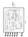
- FIG. 2 A block diagram of the architecture of this invention is depicted in Figure 2.
- the dedicated additional structures to the existent structures of the microprocessor system for managing the functions of the memory device that have been introduced according to this invention are substantially represented by the three circuit blocks: PATTERN LOGIC, FAIL LOGIC and REDUNDANCY LOGIC.
- the process that is autonomously executed by internal structures of the memory device comprises the following steps:
- the microcontroller MICRO for managing the device through the address counter ADDCNT, scans the whole array of memory cells ARRAY.
- the addresses ADDRESS generated by the address counter ADDCNT, are sent to the block PATTERN LOGIC that, in function of the chosen pattern, will output the flag TO_BE_PROG. This flag indicates to the microcontroller that the addressed location of the array must be programmed.
- the writing algorithm of the test pattern may be resumed as follows:
- Figure 3 shows the architecture of the logic that drives each LATCH_FAIL of the block.
- the driving logic of each LATCH_FAIL is input with the logic value generated on the output node SA_OUT of a respective sense amplifier of the bank of sense amplifiers SENSE of the array of memory cells and the expected logic value READ_ONE that, combined by the logic XOR gate, generate the resulting logic value READ_OK that is stored in the LATCH_FAIL.
- the fails eventually detected on the column are stored in the LATCH_FAIL and the addresses of the columns that contained fails are stored in a memory buffer RAM_TEST, in order to be successively substituted with redundancy columns.
- the read algorithm of the pattern may be resumed as follows:
- the verification mode is similar to the program mode: the addresses arrive to the PATTERN LOGIC, that will generate the flag READ_ONE that is XORed with the bit value read from the ARRAY either allowing or not to set the relative LATCH_FAIL of the block FAIL LOGIC.
- the memory buffer RAM dedicated for storing the addresses of the columns that contains a fail must have a capacity corresponding to the maximum number of redundable fails, that is an adequate number of "packets" of single memory cells each appropriate to store the address of a fail column.
- the buffer RAM_TEST may be defined in one of the RAM arrays that are normally present for other purposes in modem FLASH memory devices (for example, RAM for protections, and so on), by simply increasing its size.
- the MICRO starts communicating with the block REDUNDANCY LOGIC through the signal REDUNDANCY_RULES.
- the logic of the block REDUNDANCY LOGIC implements the column redundancy rules of the device by considering both the fail information relative to the current test pattern and written in the RAM_TEST and the fail information detected with a previously used test pattern and already permanently stored in a CAM array or (as in the shown example in Figure 2) in the PO_SECTOR.
- the die would not be redundable and the block REDUNDANCY LOGIC would send a NO_RED_POSSIBLE flag to the MICRO, that on its turn would provide through the output pad of the device, and thus to the test machine, a fail code and the processed die will eventually be discarded.
- a usable redundancy resource will be located and the MICRO will execute the algorithms for writing in the CAM array or in the PO_SECTOR the redundancy information of the new fails, relying on the information provided from the block REDUNDANCY LOGIC and on the fail addresses stored in the RAM TEST.
- the pad connections of a device with the architecture of this invention, with the EWS test machine may, compatibly with other peculiar features of the device, be significantly reduced in number.
- Figure 5 illustrates the protocol for starting up the verification process with a certain test pattern and Figure 6 illustrates the read protocol for the verification of the results.
Abstract
Description
- The market of FLASH memory devices offers very small margins for manufacturers of memory devices. Industries are studying new manufacturing techniques and methods in order to maximize at the same time both yield and productivity.
- A technique for increasing yield, used for years, consists in implementing row, column and sector redundancy. These techniques, even if they allow to increment the yield, increase relevantly the time required for testing the devices on wafer (EWS) because the test machine, besides detecting the physical position of the fail in the array, must implement a series of procedures for mapping the failed element (row, column, sector) on an available valid spare resource. This limits relevantly productivity, and for improving it further investments are made for attaining the required throughput of validated devices.
- The devices being fabricated are usually tested on wafer by using electric techniques (EWS - Electrical Wafer Sort) for determining the presence of failed elements (rows, columns, or whole sectors), and for repairing them by substituting the failed element with spare resources available on chip.
- As schematically depicted in Figure 1A, the whole test, substitution and verification process is carried out by the test machine that must establish a communication with each single die in order to:
- 1. carry out specific tests for determining the presence of eventual fails;
- 2. store (in the test machine) the position of the fails detected in the memory array of cells;
- 3. apply the redundancy rules of the particular architecture (written in the software for managing the test machine) necessary for mapping correctly the failed element on an equivalent spare (redundancy) element;
- 4. write in a nonvolatile fashion in the memory under test the information obtained in the previous steps.
- This process has mainly two evident drawbacks:
- complex test programs must be developed for carrying out the search of and implementing complex techniques for repairing eventual fails;
- the time required by the test machine for interrogating each single die to be tested, for determining eventual fails and for arranging substitution by spare resources, where it is possible, is relatively long.
- This implies that the yield increase due to the exploitation of purposely fabricated spare resources in the device (redundancy) reduces productivity, and it is possible to compensate for this reduction only by buying and installing numerous test machines.
- In order to improve productivity, architectures of memory devices that contemplate integrating in the same device dedicated structures for simplifying the operations carried out by the test machine have been proposed. The prior published
European patent application No. 1 624 465 in the name of the same applicant, discloses an architecture developed to provide a tool for the analysis of fails that may suggest possible effective modifications of certain process conditions for reducing the number of fails. - The article "Programmable Built-In Self-Testing of Embedded RAM Clusters in System-on-Chip Architectures", by A. Benso, et al., IEEE Communications Magazine, September 2003, pages 90 to 97, provides another example of these known approaches.
- These known techniques have the drawback of requiring the integration on each memory chip of complex dedicated structures such as dedicated processors for realizing a so-called BIST (Built In Self Test) system or, as in the case of the above mentioned prior application, for realizing a BISR (Built In Self Test and Self Repair) system, the realization of which implies a relevant silicon area occupation. This makes this architecture not usable on stand alone FLASH memory devices. It may be employed in systems on chip or on complex architectures of chips that include, for commercial purposes, microcontrollers and large volatile memory arrays (RAM). Moreover, these systems still contemplate an interaction with the EWS test machine for collecting verification data when reading the memory and for carrying out redundancy operations and read operations, carried out for verifying the correct functionality of memory locations, involve the whole data path of the memory device.
- On another account, modem nonvolatile FLASH memory devices (even stand alone devices) more and more often include a small microcontroller system for managing operations of the memory, comprising a microprocessor and a relative ROM storing program codes for executing the various functions, an internal address counter, one or more auxiliary RAM memory arrays, for example for managing the protection of sectors and for storing configuration information of the device that are read during the turn on phase, arrays of CAMs or a reserved sector of the non volatile memory array, inaccessible by the user, in which, during a phase of test on wafer of the device being fabricated, redundancy and configuration information of the inner circuitry and other specific parameters of the device under test are permanently written.
- An effective solution to the above mentioned problems of maximization of the production yield and of maximization of the productivity of fabrication of nonvolatile FLASH memory devices that comprise a microprocessor system for managing the functions of the memory device, has been found.
- The objective of reducing the time needed for executing the tests and substituting failed parts of the array of nonvolatile memory cells with redundancy structures, thus limiting also the interaction between the EWS test machine and each device being fabricated and without a burdensome increase of the silicon area occupied by the device is fully attained by the architecture of this invention.
- The new automatic redundance system of this invention exploits the existing management microprocessor system available on chip for carrying out automatically, without communicating with the external test machine, the operations of writing data in the memory array according to one or more preestablished test schemes, of verifying data successively read from the memory array, eventually of substituting failed elements of the array with equivalent redundant structures. The redundance system utilizes a specifically embodied logic structure for detecting and storing eventual failed elements of the array of memory cells, upstream of the output data path of the memory device that speeds up data collection of eventual fails without any interaction with the external test machine, apart from communicating the end of its task.
- Moreover, a logic circuitry that implements specific redundancy rules of the device interacts with the microprocessor of the device in order to map the failed element on an available analogous spare element, by registering data of the effected substitution in a reserved sector of memory cells or in other nonvolatile memory elements such as for example in an array of CAMs.
- The invention overcomes the above mentioned drawbacks by carrying out a writing, verification and substitution of fail elements process that, once started, is carried out in a substantially autonomous and completely automatic manner, without any intervention of an operator through the test machine. Practically, the process generates a validation or an irrecoverable-fail flag of the device being fabricated, that in the last case is discarded. The realization of the necessary dedicated structures in the device has, moreover, a very low impact on the area occupied by the device.
- The invention is defined in the annexed claims.
-
- Figure 1A shows schematically the interaction between the EWS test machine and the device under test.
- Figure 1B shows different test patterns that are commonly used for finding eventual fails in the array.
- Figure 2 is a block diagram of the architecture of this invention.
- Figure 3 is a detailed circuit scheme of the block FAIL LOGIC of the architecture of this invention.
- Figure 4 is a scheme that shows the connections of the logic circuitry of the block FAIL LOGIC at the output of the read sense amplifiers of the array.
- Figures 5 and 6 illustrate, respectively, the start-up protocol of the verification process with a certain test pattern and the read protocol of the verification results.
- The process of this invention consists in executing a certain set of algorithms, written in an internal ROM, for searching eventual electric fails in the memory cell array. These algorithms are of two types:
- 1. the task of a first type of algorithms consists in writing in the array, that is in programming the cells of the array according to a series of specific patterns such as the Checkerboad pattern, the inverted Checkerboard pattern and the Diagonal pattern, depicted in Figure 1B, besides the ALL0 pattern;
- 2. the task of a second type of algorithms consists in verifying, by a read operation, the physical state of the cells of the array in respect to internal reference states for the particular write pattern of the cells and in signaling to a control logic eventual fails (difference between the read value and the expected value) detected during the execution of the verification scanning.
- In practice, according to this invention, it is assumed that the die receive, from the test machine, a single command for starting the execution of the test routines the codes of which may be stored in the same ROM (Read Only Memory) of the management system, properly dimensioned such to start the relative scanning of the whole array from a certain address (for example 0x000000,
row 0, column 0). This means that the communication between the test machine and the die is carried out in "one shot" fashion, that is only a start-up command of the testing and fail elements substitution process is issued to the die, the internal redundancy system of which carries out the fail search tests, the storage of the fail location data in a RAM array of the device, the application of specific redundancy rules and the writing in nonvolatile storage elements present in the die, such as a CAM array or a reserved FLASH sector (called also power-on sector) of the FLASH memory array, the mapping of the element in which a fail has been detected on a certain corresponding redundancy element. - A block diagram of the architecture of this invention is depicted in Figure 2. The dedicated additional structures to the existent structures of the microprocessor system for managing the functions of the memory device that have been introduced according to this invention are substantially represented by the three circuit blocks: PATTERN LOGIC, FAIL LOGIC and REDUNDANCY LOGIC.
- For each selected test pattern, Checkerboard, Diagonal and so on, the process that is autonomously executed by internal structures of the memory device comprises the following steps:
- 1. writing a selected test pattern in the memory array;
- 2. verifying that data read from the array correspond to the written data data;
- 3. storing the address of an eventual failed element;
- 4. substituting, if possible, the failed element with a substitutive redundant element.
- The different steps will be described in detail hereinbelow referring to the circuit scheme of Figure 2.
- The microcontroller MICRO for managing the device, through the address counter ADDCNT, scans the whole array of memory cells ARRAY.
- The addresses ADDRESS, generated by the address counter ADDCNT, are sent to the block PATTERN LOGIC that, in function of the chosen pattern, will output the flag TO_BE_PROG. This flag indicates to the microcontroller that the addressed location of the array must be programmed. The writing algorithm of the test pattern may be resumed as follows:
- a) initialization, executed by the MICRO, of the address counter ADDCNT;
- b) if TO_BE_PROG=0, go to step d);
- c) if TO_BE_PROG=1, then the MICRO carries out the program algorithm;
- d) increment of the address, executed by the MICRO;
- e) if the last location of the array has not been reached, go to step b), otherwise execute the successive step.
- In this phase a verification of the correctness of the PATTERN previously written in the array ARRAY is carried out, in order to locate eventual discrepancies indicative of physical fails in the array. The verification is carried out by reading all the bits on the addressed column. An eventual discrepancy from the expected value indicates the presence of a fail in the column. This event is stored in a latch of the block FAIL LOGIC.
- Figure 3 shows the architecture of the logic that drives each LATCH_FAIL of the block. According to a main feature of the architecture of this invention, the driving logic of each LATCH_FAIL is input with the logic value generated on the output node SA_OUT of a respective sense amplifier of the bank of sense amplifiers SENSE of the array of memory cells and the expected logic value READ_ONE that, combined by the logic XOR gate, generate the resulting logic value READ_OK that is stored in the LATCH_FAIL.
- In practice, the fails eventually detected on the column are stored in the LATCH_FAIL and the addresses of the columns that contained fails are stored in a memory buffer RAM_TEST, in order to be successively substituted with redundancy columns.
- The read algorithm of the pattern may be resumed as follows:
- a) initialization, executed by the MICRO, of the address counter ADDCNT;
- b) resetting of the related LATCH_FAIL through the command RESET_FAIL_LATCH of the microprocessor;
- c) reading of the addressed bit and comparison with the expected value given by the signal READ_ONE;
- d) if the read value differs from the expected one, the LATCH_FAIL stores the event that a discrepancy between the expected value and the read value has occurred;
- e) incrementing of the row address and iteration from point (c) up to the completion of the column scanning;
- f) control of the output of the block FAIL _LOGIC:
- 1. if the output is high (presence of a FAIL), storing of the current address of the fail column in a memory buffer RAM_TEST through the write signal WRITE_FAIL,
- 2. if the output is low, the addressed column does not contain fails, and the successive step is carried out;
- g) incrementing of the column address and iteration from the step b) up to the completion of the scanning of the whole array.
- Clearly, verification may take place for a column of cells at the time or alternatively it may be carried out on a certain number N of columns, in case the memory architecture contemplate a parallelism that allows to read N columns in parallel, as indicated in the scheme of Figure 4.
- As described above, the verification mode is similar to the program mode: the addresses arrive to the PATTERN LOGIC, that will generate the flag READ_ONE that is XORed with the bit value read from the ARRAY either allowing or not to set the relative LATCH_FAIL of the block FAIL LOGIC.
- Clearly, the memory buffer RAM dedicated for storing the addresses of the columns that contains a fail must have a capacity corresponding to the maximum number of redundable fails, that is an adequate number of "packets" of single memory cells each appropriate to store the address of a fail column. The buffer RAM_TEST may be defined in one of the RAM arrays that are normally present for other purposes in modem FLASH memory devices (for example, RAM for protections, and so on), by simply increasing its size.
- When the scanning of the ARRAY is completed, the MICRO starts communicating with the block REDUNDANCY LOGIC through the signal REDUNDANCY_RULES. The logic of the block REDUNDANCY LOGIC implements the column redundancy rules of the device by considering both the fail information relative to the current test pattern and written in the RAM_TEST and the fail information detected with a previously used test pattern and already permanently stored in a CAM array or (as in the shown example in Figure 2) in the PO_SECTOR.
- If the topology of the detected fails with the test pattern just used is such to violate the redundancy rules imposed by the architecture, or the number of fail elements surpasses the number of available resources, the die would not be redundable and the block REDUNDANCY LOGIC would send a NO_RED_POSSIBLE flag to the MICRO, that on its turn would provide through the output pad of the device, and thus to the test machine, a fail code and the processed die will eventually be discarded.
- In the opposite case, a usable redundancy resource will be located and the MICRO will execute the algorithms for writing in the CAM array or in the PO_SECTOR the redundancy information of the new fails, relying on the information provided from the block REDUNDANCY LOGIC and on the fail addresses stored in the RAM TEST.
- Obviously, if the verification phase of a particular test pattern terminates without detecting any fail, the SUBSTITUTION phase is skipped.
- The advantages provided by the present invention may be resumed as follows:
- a) the intervention of the test machine is no longer required for driving the device under test for finding and mapping defects of the array on the available redundancy resources, thus it is possible to carry out the redundancy process on a plurality of devices in parallel for increasing productivity;
- b) the reduced number of connection pads machine/device under test enhance the compatibility with the test methods that may be implemented in a Low Pin Count mode;
- c) substantial reduction of the time for testing and permanently writing redundancy data compared to prior art techniques;
- d) reduction of the complexity of test programs;
- e) reduction of the time-to-market of new FLASH memory devices.
- The above advantages are attained with a modest increment of overhead area in the single devices, because test structures, logic parts, algorithms and storage devices, most of which are already present in a FLASH memory device, are exploited.
- As indicated in Figure 2, the pad connections of a device with the architecture of this invention, with the EWS test machine may, compatibly with other peculiar features of the device, be significantly reduced in number.
- Figure 5 illustrates the protocol for starting up the verification process with a certain test pattern and Figure 6 illustrates the read protocol for the verification of the results.
Claims (6)
- A memory device, comprising an array of cells (ARRAY FLASH), at least a row decoding circuit and a column decoding circuit (COL DEC) associated to a relative bank of sense amplifiers (SENSE) and incorporating a microcontroller system (MICRO) for managing erase, program, erase verify, program verify and read operations of data in said memory cell array, characterized in that it comprises
a logic circuit (FAIL LOGIC) for verifying and storing the existence of fail cells in one or more columns of the array during the execution of a test algorithm, connected to the output of each sense amplifier, comprising a logic gate (XOR) having a first input connected to the output of a respective sense amplifier and a second input suitable for receiving the expected logic value according to said test algorithm, a resettable bistable circuit (FAIL LATCH) for storing information on an eventual fail in a column, connected in cascade to said logic gate (XOR);
a pattern logic circuit (PATTERN_LOGIC) input with addresses (ADDREAD) for accessing memory locations of said array generated by an internal address counter of the management system and outputting, in function of a certain pattern for testing the integrity of the memory, command flags for programming the addressed cell sent to said microprocessor and said expected logic value applied to an input of said logic verification circuit (FAIL_LOGIC); and
a redundancy logic circuit (REDUNDANCY LOGIC) connected to and interacting with said microcontroller system for automatically substituting fail columns or generating a non rendundability flag. - The FLASH memory device of claim 1, characterized in that said logic redundancy circuit (REDUNDANCY LOGIC) implements rules in function of which fail columns eventually detected during the execution of said test algorithm are mapped on available redundancy columns of the array of cells.
- The FLASH memory device of claim 1, characterized in that said array of memory cells (ARRAY FLASH) comprises a reserved sector inaccessible by an external user on which mapping data of said fail columns are permanently written.
- The memory device of claim 1, characterized in that one or more test algorithms are programmed in a read only memory (ROM TEST) of said microprocessor system for managing the device.
- The memory device of claim 1, characterized in that said array of memory cells (ARRAY FLASH) is organized in sectors, the data storage locations of which are located by a row and a column address.
- The memory device of claim 1, characterized in that it interacts with a EWS test machine for implementing said automatic redundancy of fail columns or for signaling the non redundability and the consequent rejection of the dice only through supply pads (VCC, GND, VPP), a pad of application of a clock signal (CLK), a pad of application of chip enabling command (/CE), a pad of write enabling command (/WE) and pads of input/output enabling command and commands for inputting addresses and outputting memory data (SI/O<3:0>).
Priority Applications (2)
| Application Number | Priority Date | Filing Date | Title |
|---|---|---|---|
| EP06425503A EP1881505A1 (en) | 2006-07-20 | 2006-07-20 | Memory device with embedded microprocessor for autonomously searching and repairing failures |
| US11/780,581 US7646655B2 (en) | 2006-07-20 | 2007-07-20 | Memory device with fail search and redundancy |
Applications Claiming Priority (1)
| Application Number | Priority Date | Filing Date | Title |
|---|---|---|---|
| EP06425503A EP1881505A1 (en) | 2006-07-20 | 2006-07-20 | Memory device with embedded microprocessor for autonomously searching and repairing failures |
Publications (1)
| Publication Number | Publication Date |
|---|---|
| EP1881505A1 true EP1881505A1 (en) | 2008-01-23 |
Family
ID=37649366
Family Applications (1)
| Application Number | Title | Priority Date | Filing Date |
|---|---|---|---|
| EP06425503A Withdrawn EP1881505A1 (en) | 2006-07-20 | 2006-07-20 | Memory device with embedded microprocessor for autonomously searching and repairing failures |
Country Status (2)
| Country | Link |
|---|---|
| US (1) | US7646655B2 (en) |
| EP (1) | EP1881505A1 (en) |
Families Citing this family (12)
| Publication number | Priority date | Publication date | Assignee | Title |
|---|---|---|---|---|
| JP2006048777A (en) * | 2004-08-02 | 2006-02-16 | Toshiba Corp | Nand flash memory and data writing method |
| US8495467B1 (en) | 2009-06-30 | 2013-07-23 | Micron Technology, Inc. | Switchable on-die memory error correcting engine |
| US8412987B2 (en) * | 2009-06-30 | 2013-04-02 | Micron Technology, Inc. | Non-volatile memory to store memory remap information |
| US8412985B1 (en) | 2009-06-30 | 2013-04-02 | Micron Technology, Inc. | Hardwired remapped memory |
| US8392777B2 (en) * | 2009-08-27 | 2013-03-05 | Advanced Micro Devices, Inc. | Centralized MBIST failure information |
| US9099173B2 (en) * | 2012-12-14 | 2015-08-04 | Virtium Technology, Inc. | Classifying flash devices using ECC |
| US8929167B2 (en) | 2013-01-31 | 2015-01-06 | Qualcomm Incorporated | MRAM self-repair with BIST logic |
| US10635526B2 (en) * | 2017-06-12 | 2020-04-28 | Sandisk Technologies Llc | Multicore on-die memory microcontroller |
| US10504604B2 (en) | 2017-09-28 | 2019-12-10 | Taiwan Semiconductor Manufacturing Co., Ltd. | Systems and methods to test a memory device |
| US11899550B2 (en) | 2020-03-31 | 2024-02-13 | Advantest Corporation | Enhanced auxiliary memory mapped interface test systems and methods |
| US11650893B2 (en) * | 2020-03-31 | 2023-05-16 | Advantest Corporation | Multiple name space test systems and methods |
| CN112261388B (en) * | 2020-09-07 | 2023-08-01 | 中国电影器材有限责任公司 | Redundancy recovery method, device and system for satellite transmission digital film package |
Citations (3)
| Publication number | Priority date | Publication date | Assignee | Title |
|---|---|---|---|---|
| US20020001241A1 (en) * | 2000-06-29 | 2002-01-03 | Kazuo Hotaka | Redundancy memory circuit |
| EP1453062A1 (en) * | 2003-02-27 | 2004-09-01 | STMicroelectronics S.r.l. | Built-in testing methodology in flash memory |
| US20050034040A1 (en) * | 2003-08-07 | 2005-02-10 | Broadcom Corporation | System and method for self-adaptive redundancy choice logic |
Family Cites Families (3)
| Publication number | Priority date | Publication date | Assignee | Title |
|---|---|---|---|---|
| JP3867862B2 (en) * | 1997-04-16 | 2007-01-17 | 株式会社ルネサステクノロジ | Semiconductor integrated circuit and memory inspection method |
| US6067262A (en) * | 1998-12-11 | 2000-05-23 | Lsi Logic Corporation | Redundancy analysis for embedded memories with built-in self test and built-in self repair |
| US6879530B2 (en) * | 2002-07-18 | 2005-04-12 | Micron Technology, Inc. | Apparatus for dynamically repairing a semiconductor memory |
-
2006
- 2006-07-20 EP EP06425503A patent/EP1881505A1/en not_active Withdrawn
-
2007
- 2007-07-20 US US11/780,581 patent/US7646655B2/en active Active
Patent Citations (3)
| Publication number | Priority date | Publication date | Assignee | Title |
|---|---|---|---|---|
| US20020001241A1 (en) * | 2000-06-29 | 2002-01-03 | Kazuo Hotaka | Redundancy memory circuit |
| EP1453062A1 (en) * | 2003-02-27 | 2004-09-01 | STMicroelectronics S.r.l. | Built-in testing methodology in flash memory |
| US20050034040A1 (en) * | 2003-08-07 | 2005-02-10 | Broadcom Corporation | System and method for self-adaptive redundancy choice logic |
Also Published As
| Publication number | Publication date |
|---|---|
| US7646655B2 (en) | 2010-01-12 |
| US20080049514A1 (en) | 2008-02-28 |
Similar Documents
| Publication | Publication Date | Title |
|---|---|---|
| EP1881505A1 (en) | Memory device with embedded microprocessor for autonomously searching and repairing failures | |
| JP4761959B2 (en) | Semiconductor integrated circuit device | |
| US7463520B2 (en) | Memory device with variable trim settings | |
| US7739559B2 (en) | Semiconductor device and program data redundancy method therefor | |
| JP5013230B2 (en) | Self-healing method of nonvolatile memory device having trouble in erasing / programming and nonvolatile memory device related thereto | |
| CN101512669B (en) | Defective block isolation in a non-volatile memory system | |
| EP1453062B1 (en) | Built-in testing methodology in flash memory | |
| KR101075091B1 (en) | Semiconductor memory device and test method thereof | |
| US8095834B2 (en) | Macro and command execution from memory array | |
| US6981188B2 (en) | Non-volatile memory device with self test | |
| US6922649B2 (en) | Multiple on-chip test runs and repairs for memories | |
| US8201037B2 (en) | Semiconductor integrated circuit and method for controlling semiconductor integrated circuit | |
| US20080109594A1 (en) | Non-volatile memory device controlled by a micro-controller | |
| CN101111900B (en) | Semi-conductor device, address assignment method | |
| US9318222B2 (en) | Hierarchical, distributed built-in self-repair solution | |
| KR101967270B1 (en) | Memory device and method for testing the same | |
| EP1394810B1 (en) | Nonvolatile storage device and self-repair method for the same | |
| JP6594712B2 (en) | Semiconductor memory and method for verifying semiconductor memory | |
| US7196952B1 (en) | Column/sector redundancy CAM fast programming scheme using regular memory core array in multi-plane flash memory device | |
| CN107274931A (en) | Test the method and system of semiconductor devices | |
| TWI779610B (en) | Method for detecting flash memory module and associated system on chip | |
| US10504607B1 (en) | Multiple-channel, programmable fuse control unit | |
| JP2004039055A (en) | Nonvolatile semiconductor memory device | |
| US7434092B2 (en) | Semiconductor memory and method of storing configuration data | |
| CN116721689A (en) | Storage device with post-package repair function and repair method thereof |
Legal Events
| Date | Code | Title | Description |
|---|---|---|---|
| PUAI | Public reference made under article 153(3) epc to a published international application that has entered the european phase |
Free format text: ORIGINAL CODE: 0009012 |
|
| AK | Designated contracting states |
Kind code of ref document: A1 Designated state(s): AT BE BG CH CY CZ DE DK EE ES FI FR GB GR HU IE IS IT LI LT LU LV MC NL PL PT RO SE SI SK TR |
|
| AX | Request for extension of the european patent |
Extension state: AL BA HR MK YU |
|
| 17P | Request for examination filed |
Effective date: 20080722 |
|
| 17Q | First examination report despatched |
Effective date: 20080825 |
|
| AKX | Designation fees paid |
Designated state(s): DE GB |
|
| RAP1 | Party data changed (applicant data changed or rights of an application transferred) |
Owner name: STMICROELECTRONICS SRL |
|
| STAA | Information on the status of an ep patent application or granted ep patent |
Free format text: STATUS: THE APPLICATION IS DEEMED TO BE WITHDRAWN |
|
| 18D | Application deemed to be withdrawn |
Effective date: 20101104 |