EP1880862A1 - Screen printing plate - Google Patents
Screen printing plate Download PDFInfo
- Publication number
- EP1880862A1 EP1880862A1 EP07112629A EP07112629A EP1880862A1 EP 1880862 A1 EP1880862 A1 EP 1880862A1 EP 07112629 A EP07112629 A EP 07112629A EP 07112629 A EP07112629 A EP 07112629A EP 1880862 A1 EP1880862 A1 EP 1880862A1
- Authority
- EP
- European Patent Office
- Prior art keywords
- screen printing
- hole patterns
- printing plate
- holes
- squeegee
- Prior art date
- Legal status (The legal status is an assumption and is not a legal conclusion. Google has not performed a legal analysis and makes no representation as to the accuracy of the status listed.)
- Granted
Links
- 238000007650 screen-printing Methods 0.000 title claims abstract description 53
- 238000007639 printing Methods 0.000 claims abstract description 48
- 238000007599 discharging Methods 0.000 claims abstract description 23
- 239000007788 liquid Substances 0.000 claims abstract description 12
- 238000010018 discharge printing Methods 0.000 claims description 2
- 239000012774 insulation material Substances 0.000 claims description 2
- 238000009413 insulation Methods 0.000 description 24
- 238000000034 method Methods 0.000 description 18
- 239000011229 interlayer Substances 0.000 description 15
- 239000000758 substrate Substances 0.000 description 14
- 230000000052 comparative effect Effects 0.000 description 11
- 239000010410 layer Substances 0.000 description 9
- 239000000839 emulsion Substances 0.000 description 6
- 239000011159 matrix material Substances 0.000 description 6
- 239000004065 semiconductor Substances 0.000 description 6
- 238000004519 manufacturing process Methods 0.000 description 5
- 239000002245 particle Substances 0.000 description 5
- 239000002904 solvent Substances 0.000 description 5
- BQCADISMDOOEFD-UHFFFAOYSA-N Silver Chemical compound [Ag] BQCADISMDOOEFD-UHFFFAOYSA-N 0.000 description 4
- 239000000463 material Substances 0.000 description 4
- 239000003094 microcapsule Substances 0.000 description 4
- 229920005989 resin Polymers 0.000 description 4
- 239000011347 resin Substances 0.000 description 4
- 239000006185 dispersion Substances 0.000 description 3
- 238000001035 drying Methods 0.000 description 3
- 238000011156 evaluation Methods 0.000 description 3
- 238000011144 upstream manufacturing Methods 0.000 description 3
- XUIMIQQOPSSXEZ-UHFFFAOYSA-N Silicon Chemical compound [Si] XUIMIQQOPSSXEZ-UHFFFAOYSA-N 0.000 description 2
- 239000004020 conductor Substances 0.000 description 2
- 239000000945 filler Substances 0.000 description 2
- 230000005484 gravity Effects 0.000 description 2
- 239000011256 inorganic filler Substances 0.000 description 2
- 229910003475 inorganic filler Inorganic materials 0.000 description 2
- 238000010030 laminating Methods 0.000 description 2
- 238000000206 photolithography Methods 0.000 description 2
- 229920000642 polymer Polymers 0.000 description 2
- 230000003014 reinforcing effect Effects 0.000 description 2
- 230000000452 restraining effect Effects 0.000 description 2
- 229910052710 silicon Inorganic materials 0.000 description 2
- 239000010703 silicon Substances 0.000 description 2
- 229910052709 silver Inorganic materials 0.000 description 2
- 239000004332 silver Substances 0.000 description 2
- 239000007787 solid Substances 0.000 description 2
- DHKHKXVYLBGOIT-UHFFFAOYSA-N 1,1-Diethoxyethane Chemical compound CCOC(C)OCC DHKHKXVYLBGOIT-UHFFFAOYSA-N 0.000 description 1
- OKTJSMMVPCPJKN-UHFFFAOYSA-N Carbon Chemical compound [C] OKTJSMMVPCPJKN-UHFFFAOYSA-N 0.000 description 1
- RYGMFSIKBFXOCR-UHFFFAOYSA-N Copper Chemical compound [Cu] RYGMFSIKBFXOCR-UHFFFAOYSA-N 0.000 description 1
- 108010010803 Gelatin Proteins 0.000 description 1
- 229920000084 Gum arabic Polymers 0.000 description 1
- CTQNGGLPUBDAKN-UHFFFAOYSA-N O-Xylene Chemical compound CC1=CC=CC=C1C CTQNGGLPUBDAKN-UHFFFAOYSA-N 0.000 description 1
- 239000004642 Polyimide Substances 0.000 description 1
- 239000004372 Polyvinyl alcohol Substances 0.000 description 1
- VYPSYNLAJGMNEJ-UHFFFAOYSA-N Silicium dioxide Chemical compound O=[Si]=O VYPSYNLAJGMNEJ-UHFFFAOYSA-N 0.000 description 1
- GWEVSGVZZGPLCZ-UHFFFAOYSA-N Titan oxide Chemical compound O=[Ti]=O GWEVSGVZZGPLCZ-UHFFFAOYSA-N 0.000 description 1
- 235000010489 acacia gum Nutrition 0.000 description 1
- 239000000205 acacia gum Substances 0.000 description 1
- 239000011354 acetal resin Substances 0.000 description 1
- 239000002253 acid Substances 0.000 description 1
- -1 acryl Chemical group 0.000 description 1
- 230000002411 adverse Effects 0.000 description 1
- XAGFODPZIPBFFR-UHFFFAOYSA-N aluminium Chemical compound [Al] XAGFODPZIPBFFR-UHFFFAOYSA-N 0.000 description 1
- 229910052782 aluminium Inorganic materials 0.000 description 1
- 229910052799 carbon Inorganic materials 0.000 description 1
- 239000006229 carbon black Substances 0.000 description 1
- 238000005354 coacervation Methods 0.000 description 1
- 239000000306 component Substances 0.000 description 1
- 238000007796 conventional method Methods 0.000 description 1
- 229910052802 copper Inorganic materials 0.000 description 1
- 239000010949 copper Substances 0.000 description 1
- 230000001419 dependent effect Effects 0.000 description 1
- 230000000694 effects Effects 0.000 description 1
- 238000005401 electroluminescence Methods 0.000 description 1
- 239000012530 fluid Substances 0.000 description 1
- 229920000159 gelatin Polymers 0.000 description 1
- 239000008273 gelatin Substances 0.000 description 1
- 235000019322 gelatine Nutrition 0.000 description 1
- 235000011852 gelatine desserts Nutrition 0.000 description 1
- 239000011521 glass Substances 0.000 description 1
- 230000001771 impaired effect Effects 0.000 description 1
- 230000010354 integration Effects 0.000 description 1
- 239000004973 liquid crystal related substance Substances 0.000 description 1
- 238000012986 modification Methods 0.000 description 1
- 230000004048 modification Effects 0.000 description 1
- 239000003921 oil Substances 0.000 description 1
- 229920002037 poly(vinyl butyral) polymer Polymers 0.000 description 1
- 239000004417 polycarbonate Substances 0.000 description 1
- 229920000515 polycarbonate Polymers 0.000 description 1
- 229920006289 polycarbonate film Polymers 0.000 description 1
- 229920001721 polyimide Polymers 0.000 description 1
- 229920006324 polyoxymethylene Polymers 0.000 description 1
- 229920002451 polyvinyl alcohol Polymers 0.000 description 1
- 238000004528 spin coating Methods 0.000 description 1
- 238000012719 thermal polymerization Methods 0.000 description 1
- 229920002803 thermoplastic polyurethane Polymers 0.000 description 1
- OGIDPMRJRNCKJF-UHFFFAOYSA-N titanium oxide Inorganic materials [Ti]=O OGIDPMRJRNCKJF-UHFFFAOYSA-N 0.000 description 1
- 229920002554 vinyl polymer Polymers 0.000 description 1
- 239000004034 viscosity adjusting agent Substances 0.000 description 1
- 235000012431 wafers Nutrition 0.000 description 1
- 238000009941 weaving Methods 0.000 description 1
- 239000008096 xylene Substances 0.000 description 1
Images





Classifications
-
- B—PERFORMING OPERATIONS; TRANSPORTING
- B41—PRINTING; LINING MACHINES; TYPEWRITERS; STAMPS
- B41N—PRINTING PLATES OR FOILS; MATERIALS FOR SURFACES USED IN PRINTING MACHINES FOR PRINTING, INKING, DAMPING, OR THE LIKE; PREPARING SUCH SURFACES FOR USE AND CONSERVING THEM
- B41N1/00—Printing plates or foils; Materials therefor
- B41N1/24—Stencils; Stencil materials; Carriers therefor
-
- B—PERFORMING OPERATIONS; TRANSPORTING
- B41—PRINTING; LINING MACHINES; TYPEWRITERS; STAMPS
- B41M—PRINTING, DUPLICATING, MARKING, OR COPYING PROCESSES; COLOUR PRINTING
- B41M1/00—Inking and printing with a printer's forme
- B41M1/12—Stencil printing; Silk-screen printing
-
- B—PERFORMING OPERATIONS; TRANSPORTING
- B41—PRINTING; LINING MACHINES; TYPEWRITERS; STAMPS
- B41M—PRINTING, DUPLICATING, MARKING, OR COPYING PROCESSES; COLOUR PRINTING
- B41M3/00—Printing processes to produce particular kinds of printed work, e.g. patterns
- B41M3/003—Printing processes to produce particular kinds of printed work, e.g. patterns on optical devices, e.g. lens elements; for the production of optical devices
-
- H—ELECTRICITY
- H05—ELECTRIC TECHNIQUES NOT OTHERWISE PROVIDED FOR
- H05K—PRINTED CIRCUITS; CASINGS OR CONSTRUCTIONAL DETAILS OF ELECTRIC APPARATUS; MANUFACTURE OF ASSEMBLAGES OF ELECTRICAL COMPONENTS
- H05K3/00—Apparatus or processes for manufacturing printed circuits
- H05K3/10—Apparatus or processes for manufacturing printed circuits in which conductive material is applied to the insulating support in such a manner as to form the desired conductive pattern
- H05K3/12—Apparatus or processes for manufacturing printed circuits in which conductive material is applied to the insulating support in such a manner as to form the desired conductive pattern using thick film techniques, e.g. printing techniques to apply the conductive material or similar techniques for applying conductive paste or ink patterns
- H05K3/1216—Apparatus or processes for manufacturing printed circuits in which conductive material is applied to the insulating support in such a manner as to form the desired conductive pattern using thick film techniques, e.g. printing techniques to apply the conductive material or similar techniques for applying conductive paste or ink patterns by screen printing or stencil printing
- H05K3/1225—Screens or stencils; Holders therefor
Definitions
- the present invention relates to a screen printing plate, a thick film having through-holes, a multilayer wiring structure, and an image display apparatus.
- CMOS complementary metal-oxide-semiconductor
- CMOS complementary metal-oxide-semiconductor
- an interlayer insulation film which includes via-holes for electrical connection of wiring is used.
- an organic insulation film having a relative permittivity smaller than that of a silicone dioxide film is widely used as a material of the interlayer insulation film. Since photolithography is employed to form through-holes in the organic insulation film, however, using the organic insulation film requires a large number of steps as a manufacturing method and is disadvantageous in terms of cost.
- a squeegee is slid to discharge ink so as to perform printing with the ink deposited on a mesh (screen printing plate) having an emulsion formed in a non-discharging area from which no ink is discharged.
- the method has advantages in that the number of steps can be reduced and the usage efficiency of a material is high.
- the screen printing method is thus capable of forming fine patterns with an easy technique. Therefore, it is being used for the wiring step of transistors or the like, as well. However, it is not suitable for forming minute through-holes.
- a through-hole in a large area printing is on the order of 300 ⁇ m square using time-proven methods.
- the present invention may provide a screen printing plate capable of forming minute through-holes in a stable manner; a thick film having through-holes, which is formed by the screen printing plate; a multilayer wiring structure with a thick film having the through-holes; and an image display apparatus.
- a screen printing plate for performing printing by causing a squeegee to be slid to discharge printing liquid.
- the screen printing plate comprises: a discharging area from which printing liquid is discharged; and a non-discharging area from which no printing liquid is discharged.
- the non-discharging area is of a polygonal shape having as an apex the point with which the squeegee first comes in contact when being slid, and a width of the non-discharging area in a length direction of the squeegee increases from the apex to a maximum of the width. Accordingly, it is possible to provide the screen printing plate capable of forming minute through-holes in a stable manner.
- a screen printing plate capable of forming minute through-holes in a stable manner; a thick film having through-holes, which is formed by the screen printing plate; a multilayer wiring structure having a thick film having the through-holes; and an image display apparatus.
- a screen printing plate of an embodiment of the present invention includes through-hole patterns which are of a polygonal shape each having as an apex the point with which a squeegee first comes in contact and whose width in the length direction of the squeegee gradually increases from the apex up to the maximum of the width of the through-hole pattern when the squeegee is slid to discharge ink so as to perform printing. Accordingly, it is possible to restrain ink from oozing out under the through-hole patterns at printing and form minute through-holes in a stable manner even in a large area.
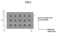
- FIG. 1 shows an example of the screen printing plate of the present invention.
- the screen printing plate as shown in FIG. 1 has regular hexagonal through-hole patterns 2 formed on a mesh 1.
- the through-hole patterns 2 are non-discharging areas of ink at printing.
- each of the through-hole patterns 2 is of a regular hexagonal shape having as the apex the point with which the squeegee first comes in contact and whose width in the length direction of the squeegee gradually increases from the apex up to the maximum of the through-hole pattern 2. Accordingly, it is possible to form a thick film having through-holes.
- the length direction of the squeegee is generally orthogonal to the printing direction.
- FIG. 2A shows an example of the through-hole pattern 2 whose side first comes in contact with the squeegee 3 in the printing direction.
- the ink flows as shown in FIG. 2A.
- the ink on the upstream side of the through-hole patterns 2 is intercepted by the through-hole patterns 2 when the squeegee 3 passes through the through-holes patterns 2.
- some of the ink is caused to ooze out under the through-hole patterns 2 by the pressure of the squeegee 3.
- the ink oozing out under the through-hole patterns 2 is printed on the areas where through-holes of a print member are to be formed and fills in the through-holes.
- the ink remaining under the through-hole patterns 2 has an adverse affect on the subsequent printing, the repeating stability of the printing would be impaired.
- the through-hole patterns 2 whose apexes first come in contact with the squeegee 3 in the printing direction, as shown in FIG. 2B.
- the ink on the upstream side of the through-hole patterns 2 can flow along both sides of the through-hole patterns 2, thereby making it is possible to restrain the ink from oozing out under the through-hole patterns 2..
- the through-hole patterns 2 are of a shape such as a circle or an ellipse having no apex as shown in FIG. 2C. Ink is less likely to ooze out under the through-hole patterns 2 compared with the case of FIG. 2A while it is more likely to ooze out under the through-hole patterns compared with that of FIG. 2B. This is because the ink in the case of FIG. 2B easily flows along both sides of the through-hole patterns 2 when the squeegee 3 passes through the through-hole patterns 2.
- the above-described effect of the screen printing plate of the present embodiment is particularly useful if the diameter of the through-hole pattern 2 is less than 300 ⁇ m, namely, if the length of the side of a minimum square including the through-hole pattern 2 is less than 300 ⁇ m. Furthermore, the minimum diameter of the through-hole pattern 2 depends on the wire diameter of the mesh 1 for use in the screen printing plate. It is thus theoretically possible to reduce the diameter of the through-hole pattern 2 as the wire diameter of the mesh 1 is reduced.
- the finest mesh 1 currently available is one obtained by weaving a wire rod having a wire diameter of about 10 ⁇ m at a density of 840 pieces per inch. As shown in FIG. 9, the diameter of the opening (discharging area) of the mesh 1 is about 20 ⁇ m.
- each of the through-hole patterns 2 In order to have the through-hole patterns 2 supported on the mesh 1, it is generally required for each of the through-hole patterns 2 to include two or more intersections of the mesh 1. This is because, if the through-hole patterns 2 include one intersection of the mesh, the mesh 1 contacts the through-hole patterns 2 at small areas, which may result in the dropping of the through-hole patterns 2 at printing.
- the through-hole patterns 2 having a diameter of 40 ⁇ m are formed on the mesh 1, for example, it is difficult for the through-hole patterns 2 to include two intersections of the mesh as shown in FIG, 9. If the through-hole patterns 2 have a diameter of 50 ⁇ m, on the other hand, it is possible for them to substantially include two or more intersections of the mesh.
- the through-hole patterns 2 having a diameter of 50 ⁇ m or more, it is possible to form minute through-holes in a stable manner even in a large area. Assuming that the wire diameter of the mesh 1 is about 15 ⁇ m, furthermore, the diameter of the through-hole pattern capable of forming minute through holes in a stable manner even in a large area is 80 ⁇ m or more.
- each of the through-hole patterns 2 is preferably axisymmetric with respect to the axis in the printing direction in the present invention. Accordingly, the ink on the upstream side of the through-hole patterns 2 can uniformly flow along both sides of the through-hole patterns 2, making it possible to further restrain the ink from oozing out under the through-hole patterns 2.
- the through-hole patterns 2 are preferably of a shape so that one or more corners other than the one including the apex with which the squeegee 3 first comes in contact are formed into a curved line, and are particularly preferably of a shape so that all the corners other than the one including the apex with which the squeegee 3 first comes in contact are formed into a curved line.
- the through-hole patterns 2 have the corners, one corner including the apex with which the squeegee 3 first comes in contact and the other ones being formed into a curved line, the ink on the outside of the through-hole patterns 2 easily smoothly flows along the curved line, thereby making it possible to further restrain the ink from oozing out under the through-hole patterns 2. Since the corners of printed through-hole patterns are formed into a curved line, the surface tension at the edge of the through-holes is equalized, thereby making it possible to restrain the occurrence of feathering caused by the fluidity of ink.
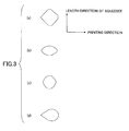
- FIGS. 3A through 3D show specific examples of such through-hole patterns 2.
- FIG. 3A shows a square in which three corners are formed into a curved line
- FIG. 3B and 3C each show a rhombus in which two corners are formed into a curved line
- FIG. 3D shows a rhombus in which three corners are formed into a curved line.
- the through-hole patterns of the screen printing plate of the present invention do not strictly match the shapes of the through-holes to be formed.
- the through-hole patterns 2 can be formed by publicly known methods. For example, it is possible to apply photolithography to the mesh 1 having a photosensitive emulsion coated thereon so as to form the through-hole patterns 2.
- a thick film having through-holes of the present embodiment is formed by performing printing with the screen printing plate of the invention. Specifically, after ink is applied to the screen printing plate arranged on a print member, the squeegee 3 is slid in the printing direction on the screen printing plate having the ink applied thereon as shown in FIG. 1. Accordingly, the ink is discharged from discharging areas other than the through-hole patterns 2 (non-discharging areas) of the mesh 1 into the print member. Subsequently, the print member having the ink discharged thereon is dried (hardened) to thereby obtain the thick film having through-holes.
- ink used for forming a thick film having through-holes is not particularly restricted, and publicly known materials containing resin components, fillers, and solvents are available.
- ink which does not easily flow at printing and drying.
- examples of the ink include one which has a viscosity of 100 Pa ⁇ s or more under the temperature condition to perform printing and a solid volume ratio of 25% or more of the ink.
- an insulation material is used to form a thick film having through-holes to thereby obtain an insulation film having the through-holes.
- a film thickness of a thick film having through-holes is determined by the formula, (thickness of mesh ⁇ opening ratio + thickness of emulsion) ⁇ solid volume ratio of ink. Accordingly, it is possible to form a thick film having a predetermined film thickness by adjusting the respective parameters as needed.
- An interlayer wiring structure of the present embodiment can be formed by laminating the thick film (interlayer insulation film) having through-holes of the invention with plural electrodes with a predetermined arrangement and electrically connecting upper and lower electrodes of the interlayer insulation film to each other via the through-holes. Accordingly, it is possible to greatly reduce the manufacturing steps and obtain a miniaturized multilayer wiring structure.
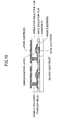
- FIG. 10 shows an example of the multilayer wiring structure of the present embodiment.
- transistors each having a gate electrode, a gate insulation film, source/drain electrodes, and semiconductor layers formed on a substrate, there is formed an interlayer insulation film having through-holes.
- a conductive layer fills in the through-holes, and the upper electrodes are formed on the interlayer insulation film.
- the upper electrodes and the conductive layer can be formed by the use of commercially-available conductive pastes containing conductive materials. Examples of the conductive materials include silver, copper, aluminum, carbon, or the like.
- An image display apparatus of the present embodiment can be formed by laminating image display elements on an active matrix substrate in which transistor elements are provided in a lattice shape, where transistors and pixel electrodes are electrically connected to each other via the through-holes through the thick film (interlayer insulation film). Accordingly, it is possible to obtain a slim and lightweight image display apparatus with an easy manufacturing process.
- a liquid crystal display element, an electrophoretic display element, and an organic EL (electroluminescence) element can be used as the image display element. Accordingly, it is possible to obtain a flat-panel type or flexible image display apparatus, which can reduce the burden on a viewer's eyes.
- FIG. 11 shows an example of the image display apparatus of the present embodiment.
- the interlayer insulation film having through-holes.
- the conductive layer fills in the through-holes, and the pixel electrodes are formed on the interlayer insulation film.
- the active matrix substrate having such a configuration, there are bonded electrophoretic display elements formed on a supporting substrate and covered by a transparent electrode.
- the screen printing plate there was employed, as the screen printing plate, one in which the square through-hole patterns 2, 200 ⁇ m on a side, were arranged in a matrix form at intervals of 400 ⁇ m (see FIG. 4) on the mesh 1 (200 mm ⁇ 200 mm) having a wire diameter of 23 ⁇ m and an opening ratio of about 50%.
- the through-hole patterns 2 are axisymmetric with respect to the axis in the printing direction as shown in FIG. 4 and have the apex with which the squeegee first comes in contact.
- the through-hole patterns 2 were by formed by exposing, developing, and drying a mesh coated with a photosensitive emulsion via a photomask having the through-hole patterns formed thereon.
- a polycarbonate film substrate (220 mm ⁇ 220 mm) having a thickness of 120 ⁇ m was dried for 60 minutes at 100°C to obtain a thick film.
- the thick film paste one prepared by dissolving a polyvinyl alcohol resin in a solvent and then adding a filler and a viscosity modifier thereto to have a viscosity of about 200 Pa ⁇ s.
- Example 1 Except that the screen printing plate as shown in FIG. 5A was used instead of that as shown in FIG. 4, a thick film was formed in the same manner as Example 1. Note that the through-hole patterns 2 are axisymmetric with respect to the axis in the printing direction as shown in FIG. 5A and have the side with which the squeegee first comes in contact.
- amorphous through-holes as shown in FIG. 5B were formed on the entire surface of the thick film.
- the formed through-holes were caused to slightly shrink in the printing direction, and they were 160 ⁇ m long ⁇ 145 ⁇ m wide on average.
- the through-hole patterns 2 of the screen printing plate as shown in FIG. 4 were changed to circular through-hole patterns having a diameter of 200 ⁇ m as shown in FIG. 6A, a thick film was formed in the same manner as Example 1. Note that the through-hole patterns are axisymmetric with respect to the axis in the printing direction as shown in FIG. 6A and have the apex with which the squeegee first comes in contact.
- the formed through-holes were 160 ⁇ m long ⁇ 160 ⁇ m wide on average.
- Through-holes were formed on the entire surface of the obtained thick film.
- the formed through-holes were caused to slightly shrink in the printing direction, and they were 160 ⁇ m long ⁇ 150 ⁇ m wide on average.
- Example 2 As compared with Example 2, it is found that although the areas of the through-hole patterns on the screen printing plate of Example 2 are smaller than those of Comparative Example 2, the through-holes formed in Example 2 are larger in size than those formed in Comparative Example 2.
- FIG. 7A there was employed, as the screen printing plate, one in which pattern units having through-hole patterns, each having a diameter of 350, 300, 250, 200, 150, 100, and 50 ⁇ m were formed on a mesh having a wire diameter of 18 ⁇ m and an opening ratio of about 40%.
- FIG. 7B 1000 pieces of two types of circular (Comparative Example 3) and droplet (Example 3) through-hole patterns were arranged in each of the pattern units at intervals of 500 ⁇ m.
- the through-hole patterns 2 were formed by exposing, developing, and drying a mesh coated with a photosensitive emulsion via a photomask having the through-hole patterns formed thereon.
- the droplet through-hole patterns (Example 3) are axisymmetric with respect to the axis in the printing direction as shown in the figure and have the apex with which the squeegee first comes in contact.
- the width of the droplet through-hole patterns in the printing direction is identical in size with that in the length direction of the squeegee.
- a washed glass substrate was dried for 30 minutes at 110°C to obtain an insulation film.
- the insulating paste one prepared by dissolving a polyvinyl butyral resin in a solvent and then adding an inorganic filler having an average particle diameter of 0.1 ⁇ m thereto to have a viscosity of about 400 Pa ⁇ s.
- the through-hole patterns As apparent from Table 1, in order to form the through-holes in a stable manner, it is required for the through-hole patterns to have a diameter of 300 ⁇ m or more in the case of Comparative Example 3 and that of 150 ⁇ m or more in the case of Example 3.
- Nano-silver ink was formed on a polycarbonate substrate by an ink jet method and then dried to form gate electrodes.
- a gate insulation film was formed by applying thermal polymerization polyimide thereto by a spin coating method and thermal-treating it at 190°C.
- the formed gate insulation film had a relative permittivity of 3.6 and a film thickness of 0.4 ⁇ m.
- Ultraviolet rays were applied to the areas, on which source/drain electrodes will be formed via a photomask, to modify the surface of the areas.
- nano-silver ink was formed on the areas by the ink jet method and then dried to form the source/drain electrodes.
- an organic semiconductor material expressed by the structural formula was dissolved in xylene to form ink.
- the resulting ink was formed into a film by the ink jet method to form an organic semiconductor layer, thereby obtaining organic transistors.
- the organic transistors thus obtained had a channel length of 5 ⁇ m and a channel width of 2 mm..
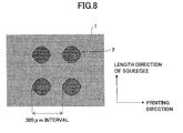
- the screen printing plate there was employed, as the screen printing plate, one in which the through-hole patterns 2 similar to those of FIG. 6A were arranged in a matrix form at intervals of 300 ⁇ m (see FIG. 8) on the mesh 1 (200 mm ⁇ 200 mm) having a wire diameter of 23 ⁇ m and an opening ratio of about 50%. Note that the through-hole patterns 2 are axisymmetric with respect to the axis in the printing direction as shown in FIG. 8 and have the apex with which the squeegee first comes in contact.
- the organic transistors were dried to obtain an interlayer insulation film having through-holes.
- the insulating paste one prepared by dissolving a polyvinyl acetal resin in a solvent and then adding an inorganic filler having an average particle diameter of 0.1 ⁇ m thereto to have a viscosity of about 400 Pa ⁇ s.
- a silver paste made of Ag particles, an acryl resin, and a solvent was formed on the interlayer insulation film by the screen printing method and then dried to fill in the through-holes of the interlayer insulation film with conductive layers and form pixel electrodes electrically connected to low-level organic transistors, thereby obtaining an active matrix substrate in which transistor elements are arranged in a lattice shape.
- the dispersion liquid prepared by dispersing the microcapsules thus obtained in a urethane resin solution was spread on a film substrate with a transparent electrode film by a wire blade method, thereby forming a uniform microcapsule sheet. Consequently an electrophoretic display element was obtained.
- the electrophoretic display element thus obtained was bonded to the active matrix substrate to obtain the image display as shown in FIG. 11.
Landscapes
- Engineering & Computer Science (AREA)
- Manufacturing & Machinery (AREA)
- Microelectronics & Electronic Packaging (AREA)
- Manufacturing Of Printed Wiring (AREA)
- Screen Printers (AREA)
- Printing Methods (AREA)
- Printing Plates And Materials Therefor (AREA)
Abstract
Description
- The present invention relates to a screen printing plate, a thick film having through-holes, a multilayer wiring structure, and an image display apparatus.
- Known semiconductor devices which have transistors and diodes on substrates or semiconductor wafers are of a multilayer wiring structure to enhance their degree of integration. In such a multilayer wiring structure, an interlayer insulation film which includes via-holes for electrical connection of wiring is used.
- In recent years and continuing, an organic insulation film having a relative permittivity smaller than that of a silicone dioxide film is widely used as a material of the interlayer insulation film. Since photolithography is employed to form through-holes in the organic insulation film, however, using the organic insulation film requires a large number of steps as a manufacturing method and is disadvantageous in terms of cost.
- In a screen printing method, on the other hand, a squeegee is slid to discharge ink so as to perform printing with the ink deposited on a mesh (screen printing plate) having an emulsion formed in a non-discharging area from which no ink is discharged. The method has advantages in that the number of steps can be reduced and the usage efficiency of a material is high. The screen printing method is thus capable of forming fine patterns with an easy technique. Therefore, it is being used for the wiring step of transistors or the like, as well. However, it is not suitable for forming minute through-holes. First, this is because it adopts a dynamic process, resulting in the ink oozing out under the non-discharging area of the screen printing plate at printing being caused to be printed on the substrate. Second, this is because the surface of fluid ink immediately after the printing becomes even due to gravity, and at the same time, a small amount of feathering is caused to occur (leveling). In forming minute through-holes, therefore, there is a high probability of the ink oozing out under the non-discharging area at printing and the ink leveling off on all sides after printing filling in the through-holes. Consequently, it is said that the limit under the conventional technique is a 100 µm square through-hole. In addition, since the screen printing method is dependent on plural parameters such as clearance (distance between the screen plate and the substrate), the angle, pressure, and speed of the squeegee, it is difficult to form minute through-holes in a stable manner; a through-hole in a large area printing is on the order of 300 µm square using time-proven methods.
- This particular screen printing method is frequently used for filling in via-holes. In
patent document 1, however, it is used for printing paste films made of a conductive paste with patterns forming island-shaped extracted portions inside the contour defining the outer shape of the paste films.. Specifically, there is employed a screen printing plate which includes, as a negative pattern of the paste film, the outside corresponding part corresponding to an outside area of the contour of the paste film, island-shaped corresponding parts corresponding to the island-shaped extracted part, and reinforcing linking parts provided to link the plural island-shaped corresponding parts with a width less than the diameter of the island-shaped corresponding part and has an emulsion area through which the conductive paste is not allowed to pass. Accordingly, it is possible to restrain print feathering from occurring. However, since the reinforcing linking parts happen to be non-discharging areas, it is not possible to perform screen printing on the entire surface other than the island-shaped parts.
[Patent Document 1]JP-B-3582480 - In view of the problem of the above-described related art, the present invention may provide a screen printing plate capable of forming minute through-holes in a stable manner; a thick film having through-holes, which is formed by the screen printing plate; a multilayer wiring structure with a thick film having the through-holes; and an image display apparatus.
- According to an aspect of the present invention, there is provided a screen printing plate for performing printing by causing a squeegee to be slid to discharge printing liquid. The screen printing plate comprises: a discharging area from which printing liquid is discharged; and a non-discharging area from which no printing liquid is discharged. In the screen printing plate, the non-discharging area is of a polygonal shape having as an apex the point with which the squeegee first comes in contact when being slid, and a width of the non-discharging area in a length direction of the squeegee increases from the apex to a maximum of the width. Accordingly, it is possible to provide the screen printing plate capable of forming minute through-holes in a stable manner.
- According to an embodiment of the present invention, it is possible to provide a screen printing plate capable of forming minute through-holes in a stable manner; a thick film having through-holes, which is formed by the screen printing plate; a multilayer wiring structure having a thick film having the through-holes; and an image display apparatus.
-
- FIG. 1 is a drawing showing an example of a screen printing plate of an embodiment of the present invention;
- FIGS. 2A through 2C are drawings describing the mechanism of restraining ink from oozing out under through-hole patterns;
- FIGS. 3A through 3D are drawings showing specific examples of through-hole patterns;
- FIG. 4 is a drawing showing the screen printing plate of Example 1;
- FIGS. 5A and 5B are drawings showing the screen printing plate of Comparative Example 1 and the formed through-holes thereof, respectively;
- FIGS. 6A and 6B are drawings showing a through-hole pattern of Example 2 and that of Comparative Example 2, respectively;
- FIGS. 7A and 7B are drawings showing the screen printing plate of Example 3 and Comparative Example 3 and the through-hole patterns thereof, respectively;
- FIG. 8 is a drawing showing the screen printing plate of Example 4;
- FIG. 9 is a drawing describing the minimum diameters of through-hole patterns;
- FIG. 10 is a drawing showing an example of the multilayer wiring structure of the present invention; and
- FIG. 11 is a drawing showing an example of the image display apparatus of the present invention.
- Next, a description is made about preferred embodiments to carry out the present invention with reference to the accompanying drawings.
- A screen printing plate of an embodiment of the present invention includes through-hole patterns which are of a polygonal shape each having as an apex the point with which a squeegee first comes in contact and whose width in the length direction of the squeegee gradually increases from the apex up to the maximum of the width of the through-hole pattern when the squeegee is slid to discharge ink so as to perform printing. Accordingly, it is possible to restrain ink from oozing out under the through-hole patterns at printing and form minute through-holes in a stable manner even in a large area.
- FIG. 1 shows an example of the screen printing plate of the present invention. The screen printing plate as shown in FIG. 1 has regular hexagonal through-
hole patterns 2 formed on amesh 1. The through-hole patterns 2 are non-discharging areas of ink at printing. In performing printing in the printing direction (direction in which thesqueegee 3 is slid) as shown in FIG. 1, each of the through-hole patterns 2 is of a regular hexagonal shape having as the apex the point with which the squeegee first comes in contact and whose width in the length direction of the squeegee gradually increases from the apex up to the maximum of the through-hole pattern 2. Accordingly, it is possible to form a thick film having through-holes. Note that the length direction of the squeegee is generally orthogonal to the printing direction. - In the present embodiment, a description is given below of the mechanism of restraining ink from oozing out under the through-
hole patterns 2 by forming the through-hole patterns 2 in such a shape and arrangement that the point with which thesqueegee 3 first comes in contact at printing is the apex" - FIG. 2A shows an example of the through-
hole pattern 2 whose side first comes in contact with thesqueegee 3 in the printing direction. When printing is performed in the printing direction of FIG. 2A to discharge ink into places other than the through-hole patterns 2, the ink flows as shown in FIG. 2A. The ink on the upstream side of the through-hole patterns 2 is intercepted by the through-hole patterns 2 when thesqueegee 3 passes through the through-holes patterns 2. However, some of the ink is caused to ooze out under the through-hole patterns 2 by the pressure of thesqueegee 3. At this time, the ink oozing out under the through-hole patterns 2 is printed on the areas where through-holes of a print member are to be formed and fills in the through-holes. In addition, since the ink remaining under the through-hole patterns 2 has an adverse affect on the subsequent printing, the repeating stability of the printing would be impaired.. - On the other hand, assume that there are formed the through-
hole patterns 2 whose apexes first come in contact with thesqueegee 3 in the printing direction, as shown in FIG. 2B. The ink on the upstream side of the through-hole patterns 2 can flow along both sides of the through-hole patterns 2, thereby making it is possible to restrain the ink from oozing out under the through-hole patterns 2.. As a result, it is possible to restrain the ink oozing out under the through-hole patterns 2 from being printed on the areas where the through-holes are to be formed and form minute through-holes in a stable manner. - Furthermore, assume that the through-
hole patterns 2 are of a shape such as a circle or an ellipse having no apex as shown in FIG. 2C. Ink is less likely to ooze out under the through-hole patterns 2 compared with the case of FIG. 2A while it is more likely to ooze out under the through-hole patterns compared with that of FIG. 2B. This is because the ink in the case of FIG. 2B easily flows along both sides of the through-hole patterns 2 when thesqueegee 3 passes through the through-hole patterns 2. - The above-described effect of the screen printing plate of the present embodiment is particularly useful if the diameter of the through-
hole pattern 2 is less than 300 µm, namely, if the length of the side of a minimum square including the through-hole pattern 2 is less than 300 µm. Furthermore, the minimum diameter of the through-hole pattern 2 depends on the wire diameter of themesh 1 for use in the screen printing plate. It is thus theoretically possible to reduce the diameter of the through-hole pattern 2 as the wire diameter of themesh 1 is reduced. Thefinest mesh 1 currently available is one obtained by weaving a wire rod having a wire diameter of about 10 µm at a density of 840 pieces per inch. As shown in FIG. 9, the diameter of the opening (discharging area) of themesh 1 is about 20 µm. In order to have the through-hole patterns 2 supported on themesh 1, it is generally required for each of the through-hole patterns 2 to include two or more intersections of themesh 1. This is because, if the through-hole patterns 2 include one intersection of the mesh, themesh 1 contacts the through-hole patterns 2 at small areas, which may result in the dropping of the through-hole patterns 2 at printing. When the through-hole patterns 2 having a diameter of 40 µm are formed on themesh 1, for example, it is difficult for the through-hole patterns 2 to include two intersections of the mesh as shown in FIG, 9. If the through-hole patterns 2 have a diameter of 50 µm, on the other hand, it is possible for them to substantially include two or more intersections of the mesh. With the through-hole patterns 2 having a diameter of 50 µm or more, it is possible to form minute through-holes in a stable manner even in a large area. Assuming that the wire diameter of themesh 1 is about 15 µm, furthermore, the diameter of the through-hole pattern capable of forming minute through holes in a stable manner even in a large area is 80 µm or more. - As shown in FIG. 1, each of the through-
hole patterns 2 is preferably axisymmetric with respect to the axis in the printing direction in the present invention. Accordingly, the ink on the upstream side of the through-hole patterns 2 can uniformly flow along both sides of the through-hole patterns 2, making it possible to further restrain the ink from oozing out under the through-hole patterns 2. - In the present embodiment, the through-
hole patterns 2 are preferably of a shape so that one or more corners other than the one including the apex with which thesqueegee 3 first comes in contact are formed into a curved line, and are particularly preferably of a shape so that all the corners other than the one including the apex with which thesqueegee 3 first comes in contact are formed into a curved line. Since with this particular preference the through-hole patterns 2 have the corners, one corner including the apex with which thesqueegee 3 first comes in contact and the other ones being formed into a curved line, the ink on the outside of the through-hole patterns 2 easily smoothly flows along the curved line, thereby making it possible to further restrain the ink from oozing out under the through-hole patterns 2. Since the corners of printed through-hole patterns are formed into a curved line, the surface tension at the edge of the through-holes is equalized, thereby making it possible to restrain the occurrence of feathering caused by the fluidity of ink. Note that although examples of the curved line in this case include a circle, an ellipse, a parabola, or the like, the curved lines are not particularly limited so long as they are projected to the outside. FIGS. 3A through 3D show specific examples of such through-hole patterns 2. FIG. 3A shows a square in which three corners are formed into a curved line, FIG. 3B and 3C each show a rhombus in which two corners are formed into a curved line, and FIG. 3D shows a rhombus in which three corners are formed into a curved line. - Note, however, that the surface of the ink discharged from the screen printing plate becomes even due to gravity, and at the same time, a small amount of feathering is caused to occur because of the principle of the screen printing method. Therefore, the through-hole patterns of the screen printing plate of the present invention do not strictly match the shapes of the through-holes to be formed.
- In the present embodiment, the through-
hole patterns 2 can be formed by publicly known methods. For example, it is possible to apply photolithography to themesh 1 having a photosensitive emulsion coated thereon so as to form the through-hole patterns 2. - A thick film having through-holes of the present embodiment is formed by performing printing with the screen printing plate of the invention. Specifically, after ink is applied to the screen printing plate arranged on a print member, the
squeegee 3 is slid in the printing direction on the screen printing plate having the ink applied thereon as shown in FIG. 1. Accordingly, the ink is discharged from discharging areas other than the through-hole patterns 2 (non-discharging areas) of themesh 1 into the print member. Subsequently, the print member having the ink discharged thereon is dried (hardened) to thereby obtain the thick film having through-holes. - In the present embodiment, ink used for forming a thick film having through-holes is not particularly restricted, and publicly known materials containing resin components, fillers, and solvents are available. In order to form through-holes, each having a diameter of 300 µm or less, it is particularly preferable to use ink which does not easily flow at printing and drying. Specifically, examples of the ink include one which has a viscosity of 100 Pa·s or more under the temperature condition to perform printing and a solid volume ratio of 25% or more of the ink.
- In the present embodiment, an insulation material is used to form a thick film having through-holes to thereby obtain an insulation film having the through-holes.
- Note that a film thickness of a thick film having through-holes is determined by the formula, (thickness of mesh × opening ratio + thickness of emulsion) × solid volume ratio of ink. Accordingly, it is possible to form a thick film having a predetermined film thickness by adjusting the respective parameters as needed.
- An interlayer wiring structure of the present embodiment can be formed by laminating the thick film (interlayer insulation film) having through-holes of the invention with plural electrodes with a predetermined arrangement and electrically connecting upper and lower electrodes of the interlayer insulation film to each other via the through-holes. Accordingly, it is possible to greatly reduce the manufacturing steps and obtain a miniaturized multilayer wiring structure. In order to have the upper and the lower electrodes of the interlayer insulation film electrically connected to each other, it is preferable to fill in the through-holes with a conductive layer. At this time, it is further preferable to form upper electrodes at the upper portions of the interlayer insulation film and fill in the through-holes with the conductive layer by the screen printing method. It is thus possible to use the same apparatus and simplify the manufacturing process.
- FIG. 10 shows an example of the multilayer wiring structure of the present embodiment. On transistors, each having a gate electrode, a gate insulation film, source/drain electrodes, and semiconductor layers formed on a substrate, there is formed an interlayer insulation film having through-holes. Moreover, a conductive layer fills in the through-holes, and the upper electrodes are formed on the interlayer insulation film. The upper electrodes and the conductive layer can be formed by the use of commercially-available conductive pastes containing conductive materials. Examples of the conductive materials include silver, copper, aluminum, carbon, or the like.
- An image display apparatus of the present embodiment can be formed by laminating image display elements on an active matrix substrate in which transistor elements are provided in a lattice shape, where transistors and pixel electrodes are electrically connected to each other via the through-holes through the thick film (interlayer insulation film). Accordingly, it is possible to obtain a slim and lightweight image display apparatus with an easy manufacturing process. Note that a liquid crystal display element, an electrophoretic display element, and an organic EL (electroluminescence) element can be used as the image display element. Accordingly, it is possible to obtain a flat-panel type or flexible image display apparatus, which can reduce the burden on a viewer's eyes.
- FIG. 11 shows an example of the image display apparatus of the present embodiment. On the transistors, each having the gate electrode, the gate insulation film, the source/drain electrodes, and the semiconductor layer formed on the substrate, there is formed the interlayer insulation film having through-holes. Moreover, the conductive layer fills in the through-holes, and the pixel electrodes are formed on the interlayer insulation film. On the active matrix substrate having such a configuration, there are bonded electrophoretic display elements formed on a supporting substrate and covered by a transparent electrode.
- There was employed, as the screen printing plate, one in which the square through-
hole patterns hole patterns 2 are axisymmetric with respect to the axis in the printing direction as shown in FIG. 4 and have the apex with which the squeegee first comes in contact. Furthermore, the through-hole patterns 2 were by formed by exposing, developing, and drying a mesh coated with a photosensitive emulsion via a photomask having the through-hole patterns formed thereon. - After being printed with the screen printing plate and a thick film paste in the printing direction as shown in FIG. 4, a polycarbonate film substrate (220 mm × 220 mm) having a thickness of 120 µm was dried for 60 minutes at 100°C to obtain a thick film. Note that there was employed, as the thick film paste, one prepared by dissolving a polyvinyl alcohol resin in a solvent and then adding a filler and a viscosity modifier thereto to have a viscosity of about 200 Pa·s.
- As a result of the evaluation of the obtained thick film with a length measuring microscope, it was found that through-holes substantially in the shape of a square were formed on the entire surface of the thick film. Note that a side of the formed through-holes was 160 µm on average.
- Except that the screen printing plate as shown in FIG. 5A was used instead of that as shown in FIG. 4, a thick film was formed in the same manner as Example 1. Note that the through-
hole patterns 2 are axisymmetric with respect to the axis in the printing direction as shown in FIG. 5A and have the side with which the squeegee first comes in contact. - As a result of the evaluation of the obtained thick film with a length measuring microscope, it was found that amorphous through-holes as shown in FIG. 5B were formed on the entire surface of the thick film. The formed through-holes were caused to slightly shrink in the printing direction, and they were 160 µm long × 145 µm wide on average.
- Except that the through-
hole patterns 2 of the screen printing plate as shown in FIG. 4 were changed to circular through-hole patterns having a diameter of 200 µm as shown in FIG. 6A, a thick film was formed in the same manner as Example 1. Note that the through-hole patterns are axisymmetric with respect to the axis in the printing direction as shown in FIG. 6A and have the apex with which the squeegee first comes in contact. - On the entire surface of the obtained thick film, there were formed through-holes having a shape substantially the same as that of the through-hole patterns" The formed through-holes were 160 µm long × 160 µm wide on average.
- Except that the through-
hole patterns 2 of the screen printing plate as shown in FIG. 4 were changed to circular through-hole patterns having a diameter of 200 µm as shown in FIG. 6B, a thick film was formed in the same manner as Example 1. - Through-holes were formed on the entire surface of the obtained thick film.. The formed through-holes were caused to slightly shrink in the printing direction, and they were 160 µm long × 150 µm wide on average.
- As compared with Example 2, it is found that although the areas of the through-hole patterns on the screen printing plate of Example 2 are smaller than those of Comparative Example 2, the through-holes formed in Example 2 are larger in size than those formed in Comparative Example 2.
- As shown in FIG. 7A, there was employed, as the screen printing plate, one in which pattern units having through-hole patterns, each having a diameter of 350, 300, 250, 200, 150, 100, and 50 µm were formed on a mesh having a wire diameter of 18 µm and an opening ratio of about 40%. Note that, as shown in FIG. 7B, 1000 pieces of two types of circular (Comparative Example 3) and droplet (Example 3) through-hole patterns were arranged in each of the pattern units at intervals of 500 µm. At this time, the through-
hole patterns 2 were formed by exposing, developing, and drying a mesh coated with a photosensitive emulsion via a photomask having the through-hole patterns formed thereon. Furthermore, the droplet through-hole patterns (Example 3) are axisymmetric with respect to the axis in the printing direction as shown in the figure and have the apex with which the squeegee first comes in contact. In addition, the width of the droplet through-hole patterns in the printing direction is identical in size with that in the length direction of the squeegee. - After being printed with the screen printing plate and an insulating paste in the printing direction as shown in FIG. 7A, a washed glass substrate was dried for 30 minutes at 110°C to obtain an insulation film. Note that there was employed, as the insulating paste, one prepared by dissolving a polyvinyl butyral resin in a solvent and then adding an inorganic filler having an average particle diameter of 0.1 µm thereto to have a viscosity of about 400 Pa·s.
- The obtained insulation film was examined under a microscope to evaluate the number of through-holes formed without being filled in each of the pattern units. Table 1 shows the evaluation results.
TABLE 1 DIAMETERS OF THROUGH-HOLE PATTERNS [µm] EXAMPLE 3 COMPARATIVE EXAMPLE 3 EXAMPLE 3 350 1000 1000 300 1000 1000 250 1000 998 200 1000 915 150 1000 780 100 995 635 50 550 360 - As apparent from Table 1, in order to form the through-holes in a stable manner, it is required for the through-hole patterns to have a diameter of 300 µm or more in the case of Comparative Example 3 and that of 150 µm or more in the case of Example 3.
- Nano-silver ink was formed on a polycarbonate substrate by an ink jet method and then dried to form gate electrodes. Next, a gate insulation film was formed by applying thermal polymerization polyimide thereto by a spin coating method and thermal-treating it at 190°C. The formed gate insulation film had a relative permittivity of 3.6 and a film thickness of 0.4 µm. Ultraviolet rays were applied to the areas, on which source/drain electrodes will be formed via a photomask, to modify the surface of the areas. In addition, nano-silver ink was formed on the areas by the ink jet method and then dried to form the source/drain electrodes. Next, an organic semiconductor material expressed by the structural formula

- There was employed, as the screen printing plate, one in which the through-
hole patterns 2 similar to those of FIG. 6A were arranged in a matrix form at intervals of 300 µm (see FIG. 8) on the mesh 1 (200 mm × 200 mm) having a wire diameter of 23 µm and an opening ratio of about 50%. Note that the through-hole patterns 2 are axisymmetric with respect to the axis in the printing direction as shown in FIG. 8 and have the apex with which the squeegee first comes in contact. - After being printed with the screen printing plate as shown in FIG. 8 and an insulating paste in the printing direction as shown in FIG. 8, the organic transistors were dried to obtain an interlayer insulation film having through-holes. Note that there was employed, as the insulating paste, one prepared by dissolving a polyvinyl acetal resin in a solvent and then adding an inorganic filler having an average particle diameter of 0.1 µm thereto to have a viscosity of about 400 Pa·s.
- In addition, a silver paste made of Ag particles, an acryl resin, and a solvent was formed on the interlayer insulation film by the screen printing method and then dried to fill in the through-holes of the interlayer insulation film with conductive layers and form pixel electrodes electrically connected to low-level organic transistors, thereby obtaining an active matrix substrate in which transistor elements are arranged in a lattice shape.
- Next, 20 parts by weight of titanium oxide, 1 part by weight of acid polymer, 2 parts by weight of silicon polymer graft carbon black MX3-GRX-001 (manufactured by Nippon Shokubai Co., Ltd.), 77 parts by weight of silicon oil KF96L-1cs (manufacture by Shin-Etsu Chemical Co., Ltd.) were mixed together and then dispersed for one hour with ultrasonic waves to obtain a dispersion liquid with black and white particles. Microcapsules were made from the dispersion liquid by a gelatin/acacia gum complex coacervation method. At this time, the average particle diameter of the microcapsules was about 60 µm. The dispersion liquid prepared by dispersing the microcapsules thus obtained in a urethane resin solution was spread on a film substrate with a transparent electrode film by a wire blade method, thereby forming a uniform microcapsule sheet. Consequently an electrophoretic display element was obtained.
- The electrophoretic display element thus obtained was bonded to the active matrix substrate to obtain the image display as shown in FIG. 11.
- The present invention is not limited to the specifically disclosed embodiments, and variations and modifications may be made without departing from the scope of the present invention.
- The present application is based on
Japanese Priority Patent Application No. 2006-195980, filed on July 18, 2006
Claims (8)
- A screen printing plate for performing printing by causing a squeegee to be slid to discharge printing liquid, comprising:a discharging area from which printing liquid is discharged; anda non-discharging area from which no printing liquid is discharged; whereinthe non-discharging area is of a polygonal shape having as an apex the point with which the squeegee first comes in contact when being slid, anda width of the non-discharging area in a length direction of the squeegee increases from the apex to a maximum of the width.
- The screen printing plate according to claim 1, characterized in that
the non-discharging area is axisymmetric with respect to the axis in the direction in which the squeegee is slid. - The screen printing plate according to claim 1, characterized in that
the non-discharging area has the shape in which one or more corners other than the apex are formed into a curved line. - The screen printing plate asccording to claim 1, characterized in that
the non-discharging area has a diameter of 50 µm or more and less than 300 µm. - A thick film having a through-hole, which is formed by printing with the screen printing plate according to claim 1.
- The thick film according to claim 5, which is made of an insulation material.
- A multilayer wiring structure which includes at least the thick film having a through-hole according to claim 5.
- An image display apparatus which includes at least the thick film having a through-hole according to claim 5.
Applications Claiming Priority (1)
| Application Number | Priority Date | Filing Date | Title |
|---|---|---|---|
| JP2006195980A JP5374810B2 (en) | 2006-07-18 | 2006-07-18 | Screen printing version |
Publications (2)
| Publication Number | Publication Date |
|---|---|
| EP1880862A1 true EP1880862A1 (en) | 2008-01-23 |
| EP1880862B1 EP1880862B1 (en) | 2011-01-05 |
Family
ID=38370907
Family Applications (1)
| Application Number | Title | Priority Date | Filing Date |
|---|---|---|---|
| EP07112629A Ceased EP1880862B1 (en) | 2006-07-18 | 2007-07-17 | Screen printing plate |
Country Status (4)
| Country | Link |
|---|---|
| US (1) | US20080017053A1 (en) |
| EP (1) | EP1880862B1 (en) |
| JP (1) | JP5374810B2 (en) |
| DE (1) | DE602007011693D1 (en) |
Families Citing this family (46)
| Publication number | Priority date | Publication date | Assignee | Title |
|---|---|---|---|---|
| US20090078458A1 (en) * | 2007-09-21 | 2009-03-26 | Ricoh Company, Ltd. | Paste composition, insulating film, multilayer interconnection structure, printed-circuit board, image display device, and manufacturing method of paste composition |
| JP5446131B2 (en) * | 2008-05-28 | 2014-03-19 | 株式会社リコー | Screen plate and method for forming a plurality of individual electrodes |
| JP4898748B2 (en) * | 2008-07-18 | 2012-03-21 | 株式会社リコー | Screen plate, interlayer insulating film, circuit board, active matrix circuit board, and image display device |
| EP2658680B1 (en) | 2010-12-31 | 2020-12-09 | Saint-Gobain Ceramics & Plastics, Inc. | Abrasive articles comprising abrasive particles having particular shapes and methods of forming such articles |
| WO2013003831A2 (en) | 2011-06-30 | 2013-01-03 | Saint-Gobain Ceramics & Plastics, Inc. | Liquid phase sintered silicon carbide abrasive particles |
| WO2013003830A2 (en) | 2011-06-30 | 2013-01-03 | Saint-Gobain Ceramics & Plastics, Inc. | Abrasive articles including abrasive particles of silicon nitride |
| US9517546B2 (en) | 2011-09-26 | 2016-12-13 | Saint-Gobain Ceramics & Plastics, Inc. | Abrasive articles including abrasive particulate materials, coated abrasives using the abrasive particulate materials and methods of forming |
| KR20140106737A (en) | 2011-12-30 | 2014-09-03 | 생-고뱅 세라믹스 앤드 플라스틱스, 인코포레이티드 | Forming shaped abrasive particles |
| PL2797716T3 (en) | 2011-12-30 | 2021-07-05 | Saint-Gobain Ceramics & Plastics, Inc. | Composite shaped abrasive particles and method of forming same |
| KR102074138B1 (en) | 2011-12-30 | 2020-02-07 | 생-고뱅 세라믹스 앤드 플라스틱스, 인코포레이티드 | Shaped abrasive particle and method of forming same |
| EP2802436B1 (en) | 2012-01-10 | 2019-09-25 | Saint-Gobain Ceramics & Plastics, Inc. | Abrasive particles having complex shapes |
| US8840696B2 (en) | 2012-01-10 | 2014-09-23 | Saint-Gobain Ceramics & Plastics, Inc. | Abrasive particles having particular shapes and methods of forming such particles |
| WO2013149209A1 (en) | 2012-03-30 | 2013-10-03 | Saint-Gobain Abrasives, Inc. | Abrasive products having fibrillated fibers |
| KR101813466B1 (en) | 2012-05-23 | 2017-12-29 | 생-고뱅 세라믹스 앤드 플라스틱스, 인코포레이티드 | Shaped abrasive particles and methods of forming same |
| WO2014005120A1 (en) | 2012-06-29 | 2014-01-03 | Saint-Gobain Ceramics & Plastics, Inc. | Abrasive particles having particular shapes and methods of forming such particles |
| EP2906392B1 (en) | 2012-10-15 | 2025-04-16 | Saint-Gobain Abrasives, Inc. | Abrasive particles having particular shapes and methods of forming such particles |
| CN104994995B (en) | 2012-12-31 | 2018-12-14 | 圣戈本陶瓷及塑料股份有限公司 | Granular materials and forming method thereof |
| WO2014161001A1 (en) | 2013-03-29 | 2014-10-02 | Saint-Gobain Abrasives, Inc. | Abrasive particles having particular shapes and methods of forming such particles |
| TW201502263A (en) | 2013-06-28 | 2015-01-16 | Saint Gobain Ceramics | Abrasive article including shaped abrasive particles |
| CN111978921A (en) | 2013-09-30 | 2020-11-24 | 圣戈本陶瓷及塑料股份有限公司 | Shaped abrasive particles and methods of forming the same |
| KR102081045B1 (en) | 2013-12-31 | 2020-02-26 | 생-고뱅 어브레이시브즈, 인코포레이티드 | Abrasive article including shaped abrasive particles |
| US9771507B2 (en) | 2014-01-31 | 2017-09-26 | Saint-Gobain Ceramics & Plastics, Inc. | Shaped abrasive particle including dopant material and method of forming same |
| AU2015247739B2 (en) | 2014-04-14 | 2017-10-26 | Saint-Gobain Ceramics & Plastics, Inc. | Abrasive article including shaped abrasive particles |
| AU2015247826A1 (en) | 2014-04-14 | 2016-11-10 | Saint-Gobain Ceramics & Plastics, Inc. | Abrasive article including shaped abrasive particles |
| WO2015184355A1 (en) | 2014-05-30 | 2015-12-03 | Saint-Gobain Abrasives, Inc. | Method of using an abrasive article including shaped abrasive particles |
| US9914864B2 (en) | 2014-12-23 | 2018-03-13 | Saint-Gobain Ceramics & Plastics, Inc. | Shaped abrasive particles and method of forming same |
| US9707529B2 (en) | 2014-12-23 | 2017-07-18 | Saint-Gobain Ceramics & Plastics, Inc. | Composite shaped abrasive particles and method of forming same |
| US9676981B2 (en) | 2014-12-24 | 2017-06-13 | Saint-Gobain Ceramics & Plastics, Inc. | Shaped abrasive particle fractions and method of forming same |
| TWI634200B (en) | 2015-03-31 | 2018-09-01 | 聖高拜磨料有限公司 | Fixed abrasive article and method of forming same |
| US10196551B2 (en) | 2015-03-31 | 2019-02-05 | Saint-Gobain Abrasives, Inc. | Fixed abrasive articles and methods of forming same |
| EP3307483B1 (en) | 2015-06-11 | 2020-06-17 | Saint-Gobain Ceramics&Plastics, Inc. | Abrasive article including shaped abrasive particles |
| JP6679306B2 (en) * | 2015-12-28 | 2020-04-15 | シャープ株式会社 | Method of manufacturing light emitting device |
| KR102313436B1 (en) | 2016-05-10 | 2021-10-19 | 생-고뱅 세라믹스 앤드 플라스틱스, 인코포레이티드 | Abrasive particles and method of forming the same |
| EP4071224A3 (en) | 2016-05-10 | 2023-01-04 | Saint-Gobain Ceramics and Plastics, Inc. | Methods of forming abrasive articles |
| EP4349896A3 (en) | 2016-09-29 | 2024-06-12 | Saint-Gobain Abrasives, Inc. | Fixed abrasive articles and methods of forming same |
| US10563105B2 (en) | 2017-01-31 | 2020-02-18 | Saint-Gobain Ceramics & Plastics, Inc. | Abrasive article including shaped abrasive particles |
| US10759024B2 (en) | 2017-01-31 | 2020-09-01 | Saint-Gobain Ceramics & Plastics, Inc. | Abrasive article including shaped abrasive particles |
| CN110719946B (en) | 2017-06-21 | 2022-07-15 | 圣戈本陶瓷及塑料股份有限公司 | Particulate material and method of forming the same |
| CN108958564A (en) * | 2018-07-27 | 2018-12-07 | 京东方科技集团股份有限公司 | A kind of printing screen plate, touch panel, its production method and display device |
| WO2021133876A1 (en) | 2019-12-27 | 2021-07-01 | Saint-Gobain Ceramics & Plastics, Inc. | Abrasive articles and methods of forming same |
| EP4081370A4 (en) | 2019-12-27 | 2024-04-24 | Saint-Gobain Ceramics & Plastics Inc. | Abrasive articles and methods of forming same |
| US11926019B2 (en) | 2019-12-27 | 2024-03-12 | Saint-Gobain Ceramics & Plastics, Inc. | Abrasive articles and methods of forming same |
| JP7478262B2 (en) * | 2020-12-24 | 2024-05-02 | 京セラ株式会社 | Screen printing plate making and screen printing equipment |
| MX2024007593A (en) | 2021-12-30 | 2024-08-20 | Saint Gobain Abrasives Inc | Abrasive articles and methods of forming same. |
| EP4457054A4 (en) | 2021-12-30 | 2026-01-14 | Saint Gobain Abrasives Inc | Grinding articles and methods for shaping them |
| CN118591436A (en) | 2021-12-30 | 2024-09-03 | 圣戈班磨料磨具有限公司 | Abrasive article and method of forming the same |
Citations (3)
| Publication number | Priority date | Publication date | Assignee | Title |
|---|---|---|---|---|
| DE2256263A1 (en) * | 1971-11-18 | 1973-05-24 | Martino Manfredini | Screen print plates mass prodn - for ceramic ind using pvc to seal nonpatterned meshes |
| JP2002160467A (en) * | 2000-11-27 | 2002-06-04 | Murata Mfg Co Ltd | Screen printing plate, method for screen printing and laminated capacitor |
| US20030124757A1 (en) * | 2001-12-27 | 2003-07-03 | Lee Yun Bok | Method of forming pattern |
Family Cites Families (13)
| Publication number | Priority date | Publication date | Assignee | Title |
|---|---|---|---|---|
| US203992A (en) * | 1878-05-21 | Improvement in stencil-plates | ||
| US338621A (en) * | 1886-03-23 | Stencil | ||
| US631634A (en) * | 1899-06-16 | 1899-08-22 | Albert Haberstroh | Stencil. |
| US1808986A (en) * | 1929-04-29 | 1931-06-09 | Ralph W Hunter | Stencil |
| GB1547967A (en) * | 1975-07-26 | 1979-07-04 | Engineering Components Ltd | Screen printing |
| CH603361A5 (en) * | 1975-11-10 | 1978-08-15 | Iten K Ag | |
| US4174664A (en) * | 1978-05-08 | 1979-11-20 | Milliken Research Corporation | Cylindrical screen having aperatures with geometric centers defined by arrays of equilateral triangles |
| US4953460A (en) * | 1989-10-02 | 1990-09-04 | At&T Bell Laboratories | Method and apparatus for screen printing |
| JP2000147781A (en) * | 1998-11-06 | 2000-05-26 | Ngk Insulators Ltd | Screen mask, its production and wiring base board |
| JP2003078248A (en) * | 2001-08-31 | 2003-03-14 | Noritake Co Ltd | Method of manufacturing thick-film multilayer substrate having via-hole |
| JP2006062117A (en) * | 2004-08-25 | 2006-03-09 | Ricoh Microelectronics Co Ltd | Printing device/method, method for manufacturing printing mask used in printing device/method |
| JP4994727B2 (en) * | 2005-09-08 | 2012-08-08 | 株式会社リコー | Organic transistor active substrate, manufacturing method thereof, and electrophoretic display using the organic transistor active substrate |
| JP2008023716A (en) * | 2006-07-18 | 2008-02-07 | Dainippon Printing Co Ltd | Screen plate and printing material |
-
2006
- 2006-07-18 JP JP2006195980A patent/JP5374810B2/en not_active Expired - Fee Related
-
2007
- 2007-07-10 US US11/775,448 patent/US20080017053A1/en not_active Abandoned
- 2007-07-17 DE DE602007011693T patent/DE602007011693D1/en active Active
- 2007-07-17 EP EP07112629A patent/EP1880862B1/en not_active Ceased
Patent Citations (3)
| Publication number | Priority date | Publication date | Assignee | Title |
|---|---|---|---|---|
| DE2256263A1 (en) * | 1971-11-18 | 1973-05-24 | Martino Manfredini | Screen print plates mass prodn - for ceramic ind using pvc to seal nonpatterned meshes |
| JP2002160467A (en) * | 2000-11-27 | 2002-06-04 | Murata Mfg Co Ltd | Screen printing plate, method for screen printing and laminated capacitor |
| US20030124757A1 (en) * | 2001-12-27 | 2003-07-03 | Lee Yun Bok | Method of forming pattern |
Also Published As
| Publication number | Publication date |
|---|---|
| DE602007011693D1 (en) | 2011-02-17 |
| US20080017053A1 (en) | 2008-01-24 |
| JP5374810B2 (en) | 2013-12-25 |
| EP1880862B1 (en) | 2011-01-05 |
| JP2008023748A (en) | 2008-02-07 |
Similar Documents
| Publication | Publication Date | Title |
|---|---|---|
| EP1880862B1 (en) | Screen printing plate | |
| EP1859662B1 (en) | Method of manufacturing a multilayer wiring structure | |
| CN1288767C (en) | Patterning method | |
| US8071432B2 (en) | Organic transistor active substrate, manufacturing method thereof, and electrophoretic display | |
| US20090026634A1 (en) | Electronic part mounting structure and its manufacturing method | |
| EP2307199B1 (en) | Screen printing plate and printing method | |
| KR100956090B1 (en) | Method of manufacturing multilevel interconnect structure and multilevel interconnect structure | |
| CN1707811A (en) | Manufacturing method of printed transistor | |
| EP2533103B1 (en) | Method of manufacturing interconnection member and electronic device, interconnection member, multilayered interconnections, electronic device, electronic device array and display device using the method | |
| US7615481B2 (en) | Method of manufacturing multilevel interconnect structure and multilevel interconnect structure | |
| CN1799292A (en) | Substrate and its manufacturing method | |
| US20090078458A1 (en) | Paste composition, insulating film, multilayer interconnection structure, printed-circuit board, image display device, and manufacturing method of paste composition | |
| JP2009272437A (en) | Laminated structure, semiconductor device, laminated structure manufacturing method, and semiconductor device manufacturing method | |
| JP5434510B2 (en) | Circuit board, image display apparatus, circuit board manufacturing method, and image display apparatus manufacturing method | |
| WO2023039882A1 (en) | Display panel and preparation method therefor | |
| CN113296316A (en) | Array substrate and display panel | |
| WO2005107346A1 (en) | Component placement substrate and production method thereof | |
| CN215576035U (en) | Array substrate, display panel | |
| JP4939030B2 (en) | Thick film having through-hole and method for producing thick film having through-hole | |
| JP5887881B2 (en) | Wiring formation method | |
| KR101015549B1 (en) | Manufacturing method of dye-sensitized solar cell | |
| JP4293031B2 (en) | Manufacturing method of electronic component mounting structure | |
| JP2010170041A (en) | Multilayer wiring structure, method for manufacturing the same, and display apparatus | |
| JP2009271311A (en) | Method for manufacturing circuit board, circuit board, active matrix circuit board, and image display device | |
| JP6671335B2 (en) | Functional film patterning method and electronic device manufacturing method |
Legal Events
| Date | Code | Title | Description |
|---|---|---|---|
| PUAI | Public reference made under article 153(3) epc to a published international application that has entered the european phase |
Free format text: ORIGINAL CODE: 0009012 |
|
| AK | Designated contracting states |
Kind code of ref document: A1 Designated state(s): AT BE BG CH CY CZ DE DK EE ES FI FR GB GR HU IE IS IT LI LT LU LV MC MT NL PL PT RO SE SI SK TR |
|
| AX | Request for extension of the european patent |
Extension state: AL BA HR MK YU |
|
| 17P | Request for examination filed |
Effective date: 20080310 |
|
| 17Q | First examination report despatched |
Effective date: 20080821 |
|
| AKX | Designation fees paid |
Designated state(s): DE ES FR GB IT NL |
|
| GRAP | Despatch of communication of intention to grant a patent |
Free format text: ORIGINAL CODE: EPIDOSNIGR1 |
|
| GRAS | Grant fee paid |
Free format text: ORIGINAL CODE: EPIDOSNIGR3 |
|
| GRAA | (expected) grant |
Free format text: ORIGINAL CODE: 0009210 |
|
| AK | Designated contracting states |
Kind code of ref document: B1 Designated state(s): DE ES FR GB IT NL |
|
| REG | Reference to a national code |
Ref country code: GB Ref legal event code: FG4D |
|
| RIN2 | Information on inventor provided after grant (corrected) |
Inventor name: ARAUMI, MAYUKA Inventor name: MURAKAMI, AKISHIGE |
|
| REF | Corresponds to: |
Ref document number: 602007011693 Country of ref document: DE Date of ref document: 20110217 Kind code of ref document: P |
|
| REG | Reference to a national code |
Ref country code: DE Ref legal event code: R096 Ref document number: 602007011693 Country of ref document: DE Effective date: 20110217 |
|
| REG | Reference to a national code |
Ref country code: NL Ref legal event code: VDEP Effective date: 20110105 |
|
| PG25 | Lapsed in a contracting state [announced via postgrant information from national office to epo] |
Ref country code: ES Free format text: LAPSE BECAUSE OF FAILURE TO SUBMIT A TRANSLATION OF THE DESCRIPTION OR TO PAY THE FEE WITHIN THE PRESCRIBED TIME-LIMIT Effective date: 20110416 |
|
| PG25 | Lapsed in a contracting state [announced via postgrant information from national office to epo] |
Ref country code: NL Free format text: LAPSE BECAUSE OF FAILURE TO SUBMIT A TRANSLATION OF THE DESCRIPTION OR TO PAY THE FEE WITHIN THE PRESCRIBED TIME-LIMIT Effective date: 20110105 |
|
| PLBE | No opposition filed within time limit |
Free format text: ORIGINAL CODE: 0009261 |
|
| STAA | Information on the status of an ep patent application or granted ep patent |
Free format text: STATUS: NO OPPOSITION FILED WITHIN TIME LIMIT |
|
| 26N | No opposition filed |
Effective date: 20111006 |
|
| PG25 | Lapsed in a contracting state [announced via postgrant information from national office to epo] |
Ref country code: IT Free format text: LAPSE BECAUSE OF FAILURE TO SUBMIT A TRANSLATION OF THE DESCRIPTION OR TO PAY THE FEE WITHIN THE PRESCRIBED TIME-LIMIT Effective date: 20110105 |
|
| REG | Reference to a national code |
Ref country code: DE Ref legal event code: R097 Ref document number: 602007011693 Country of ref document: DE Effective date: 20111006 |
|
| REG | Reference to a national code |
Ref country code: DE Ref legal event code: R082 Ref document number: 602007011693 Country of ref document: DE Representative=s name: MEISSNER BOLTE PATENTANWAELTE RECHTSANWAELTE P, DE Ref country code: DE Ref legal event code: R082 Ref document number: 602007011693 Country of ref document: DE Representative=s name: MEISSNER, BOLTE & PARTNER GBR, DE |
|
| REG | Reference to a national code |
Ref country code: DE Ref legal event code: R082 Ref document number: 602007011693 Country of ref document: DE Representative=s name: MEISSNER, BOLTE & PARTNER GBR, DE |
|
| REG | Reference to a national code |
Ref country code: FR Ref legal event code: PLFP Year of fee payment: 10 |
|
| REG | Reference to a national code |
Ref country code: FR Ref legal event code: PLFP Year of fee payment: 11 |
|
| REG | Reference to a national code |
Ref country code: FR Ref legal event code: PLFP Year of fee payment: 12 |
|
| PGFP | Annual fee paid to national office [announced via postgrant information from national office to epo] |
Ref country code: FR Payment date: 20180725 Year of fee payment: 12 Ref country code: DE Payment date: 20180723 Year of fee payment: 12 |
|
| PGFP | Annual fee paid to national office [announced via postgrant information from national office to epo] |
Ref country code: GB Payment date: 20180719 Year of fee payment: 12 |
|
| REG | Reference to a national code |
Ref country code: DE Ref legal event code: R119 Ref document number: 602007011693 Country of ref document: DE |
|
| GBPC | Gb: european patent ceased through non-payment of renewal fee |
Effective date: 20190717 |
|
| PG25 | Lapsed in a contracting state [announced via postgrant information from national office to epo] |
Ref country code: DE Free format text: LAPSE BECAUSE OF NON-PAYMENT OF DUE FEES Effective date: 20200201 Ref country code: GB Free format text: LAPSE BECAUSE OF NON-PAYMENT OF DUE FEES Effective date: 20190717 |
|
| PG25 | Lapsed in a contracting state [announced via postgrant information from national office to epo] |
Ref country code: FR Free format text: LAPSE BECAUSE OF NON-PAYMENT OF DUE FEES Effective date: 20190731 |