EP1878694A2 - Method of nanostructuring the surface of a substrate - Google Patents
Method of nanostructuring the surface of a substrate Download PDFInfo
- Publication number
- EP1878694A2 EP1878694A2 EP07112226A EP07112226A EP1878694A2 EP 1878694 A2 EP1878694 A2 EP 1878694A2 EP 07112226 A EP07112226 A EP 07112226A EP 07112226 A EP07112226 A EP 07112226A EP 1878694 A2 EP1878694 A2 EP 1878694A2
- Authority
- EP
- European Patent Office
- Prior art keywords
- substrate
- implants
- process according
- crystalline
- thermally
- Prior art date
- Legal status (The legal status is an assumption and is not a legal conclusion. Google has not performed a legal analysis and makes no representation as to the accuracy of the status listed.)
- Withdrawn
Links
Images


Classifications
-
- B—PERFORMING OPERATIONS; TRANSPORTING
- B81—MICROSTRUCTURAL TECHNOLOGY
- B81C—PROCESSES OR APPARATUS SPECIALLY ADAPTED FOR THE MANUFACTURE OR TREATMENT OF MICROSTRUCTURAL DEVICES OR SYSTEMS
- B81C1/00—Manufacture or treatment of devices or systems in or on a substrate
- B81C1/00436—Shaping materials, i.e. techniques for structuring the substrate or the layers on the substrate
- B81C1/00634—Processes for shaping materials not provided for in groups B81C1/00444 - B81C1/00626
-
- H—ELECTRICITY
- H01—ELECTRIC ELEMENTS
- H01L—SEMICONDUCTOR DEVICES NOT COVERED BY CLASS H10
- H01L21/00—Processes or apparatus adapted for the manufacture or treatment of semiconductor or solid state devices or of parts thereof
- H01L21/02—Manufacture or treatment of semiconductor devices or of parts thereof
- H01L21/04—Manufacture or treatment of semiconductor devices or of parts thereof the devices having at least one potential-jump barrier or surface barrier, e.g. PN junction, depletion layer or carrier concentration layer
- H01L21/18—Manufacture or treatment of semiconductor devices or of parts thereof the devices having at least one potential-jump barrier or surface barrier, e.g. PN junction, depletion layer or carrier concentration layer the devices having semiconductor bodies comprising elements of Group IV of the Periodic System or AIIIBV compounds with or without impurities, e.g. doping materials
- H01L21/22—Diffusion of impurity materials, e.g. doping materials, electrode materials, into or out of a semiconductor body, or between semiconductor regions; Interactions between two or more impurities; Redistribution of impurities
- H01L21/221—Diffusion of impurity materials, e.g. doping materials, electrode materials, into or out of a semiconductor body, or between semiconductor regions; Interactions between two or more impurities; Redistribution of impurities of killers
-
- H—ELECTRICITY
- H01—ELECTRIC ELEMENTS
- H01L—SEMICONDUCTOR DEVICES NOT COVERED BY CLASS H10
- H01L21/00—Processes or apparatus adapted for the manufacture or treatment of semiconductor or solid state devices or of parts thereof
- H01L21/02—Manufacture or treatment of semiconductor devices or of parts thereof
- H01L21/04—Manufacture or treatment of semiconductor devices or of parts thereof the devices having at least one potential-jump barrier or surface barrier, e.g. PN junction, depletion layer or carrier concentration layer
- H01L21/18—Manufacture or treatment of semiconductor devices or of parts thereof the devices having at least one potential-jump barrier or surface barrier, e.g. PN junction, depletion layer or carrier concentration layer the devices having semiconductor bodies comprising elements of Group IV of the Periodic System or AIIIBV compounds with or without impurities, e.g. doping materials
- H01L21/26—Bombardment with radiation
- H01L21/263—Bombardment with radiation with high-energy radiation
- H01L21/265—Bombardment with radiation with high-energy radiation producing ion implantation
- H01L21/26506—Bombardment with radiation with high-energy radiation producing ion implantation in group IV semiconductors
-
- H—ELECTRICITY
- H01—ELECTRIC ELEMENTS
- H01L—SEMICONDUCTOR DEVICES NOT COVERED BY CLASS H10
- H01L21/00—Processes or apparatus adapted for the manufacture or treatment of semiconductor or solid state devices or of parts thereof
- H01L21/02—Manufacture or treatment of semiconductor devices or of parts thereof
- H01L21/04—Manufacture or treatment of semiconductor devices or of parts thereof the devices having at least one potential-jump barrier or surface barrier, e.g. PN junction, depletion layer or carrier concentration layer
- H01L21/18—Manufacture or treatment of semiconductor devices or of parts thereof the devices having at least one potential-jump barrier or surface barrier, e.g. PN junction, depletion layer or carrier concentration layer the devices having semiconductor bodies comprising elements of Group IV of the Periodic System or AIIIBV compounds with or without impurities, e.g. doping materials
- H01L21/26—Bombardment with radiation
- H01L21/263—Bombardment with radiation with high-energy radiation
- H01L21/265—Bombardment with radiation with high-energy radiation producing ion implantation
- H01L21/2654—Bombardment with radiation with high-energy radiation producing ion implantation in AIIIBV compounds
-
- H—ELECTRICITY
- H01—ELECTRIC ELEMENTS
- H01L—SEMICONDUCTOR DEVICES NOT COVERED BY CLASS H10
- H01L21/00—Processes or apparatus adapted for the manufacture or treatment of semiconductor or solid state devices or of parts thereof
- H01L21/02—Manufacture or treatment of semiconductor devices or of parts thereof
- H01L21/04—Manufacture or treatment of semiconductor devices or of parts thereof the devices having at least one potential-jump barrier or surface barrier, e.g. PN junction, depletion layer or carrier concentration layer
- H01L21/18—Manufacture or treatment of semiconductor devices or of parts thereof the devices having at least one potential-jump barrier or surface barrier, e.g. PN junction, depletion layer or carrier concentration layer the devices having semiconductor bodies comprising elements of Group IV of the Periodic System or AIIIBV compounds with or without impurities, e.g. doping materials
- H01L21/26—Bombardment with radiation
- H01L21/263—Bombardment with radiation with high-energy radiation
- H01L21/268—Bombardment with radiation with high-energy radiation using electromagnetic radiation, e.g. laser radiation
-
- B—PERFORMING OPERATIONS; TRANSPORTING
- B81—MICROSTRUCTURAL TECHNOLOGY
- B81B—MICROSTRUCTURAL DEVICES OR SYSTEMS, e.g. MICROMECHANICAL DEVICES
- B81B2203/00—Basic microelectromechanical structures
- B81B2203/03—Static structures
- B81B2203/0323—Grooves
- B81B2203/033—Trenches
-
- B—PERFORMING OPERATIONS; TRANSPORTING
- B81—MICROSTRUCTURAL TECHNOLOGY
- B81C—PROCESSES OR APPARATUS SPECIALLY ADAPTED FOR THE MANUFACTURE OR TREATMENT OF MICROSTRUCTURAL DEVICES OR SYSTEMS
- B81C2201/00—Manufacture or treatment of microstructural devices or systems
- B81C2201/01—Manufacture or treatment of microstructural devices or systems in or on a substrate
- B81C2201/0101—Shaping material; Structuring the bulk substrate or layers on the substrate; Film patterning
- B81C2201/0147—Film patterning
- B81C2201/0154—Film patterning other processes for film patterning not provided for in B81C2201/0149 - B81C2201/015
Definitions
- the present invention relates to a method for nanostructuring the surface of a substrate.
- Many applications in nanotechnology use nanostructures organized for example in microelectronics, optoelectronics or biology. These nanostructures are generally obtained by growth or by deposition on the surface of a substrate. It seeks to control as accurately as possible the density and the period of these nanostructures distributed on the surface of the substrate.
- this nanostructuring can be a pre-engraving as described in the article Controlled arrangement of self-organized Si (001) substrates G. Lin et al. Applied Physics Letters, vol.75, No. 18, pages 2752 to 2754 or for example in the article "Templated Self-Assembly of Block Copolymers: Effect of Substrate Topography” Joy Y. Cheng et al. Advanced Materials 2003, 15, No. 19, October 2, pages 1599-1602 .
- periodic surface nanostructuring it is meant that periodic patterns are produced at the nanoscale at the surface of the host substrate.
- Performing a pre-etching of the host substrate is a simple way of controlling the spatial ordering of the nanostructures during the growth or deposition step.
- This pre-engraving leads to a topographic nanostructuring of the starting substrate, that is to say an embodiment of periodic patterns in relief.
- the bonding is done so as to obtain covalent bonds between the two crystal lattices of the faces to be assembled.
- An arrangement is obtained provided with a grain boundary at the bonding interface and this grain boundary thus causes the appearance of a network of dislocations whose characteristics: orientation, period, type of dislocations, symmetry, depend only on characteristics of the crystalline meshes of the substrate and of the film as well as the angles of disorientation in torsion and bending introduced during bonding. For example, starting from a film and a silicon substrate whose faces to be assembled are oriented in the ⁇ 001> direction, without disorientation of bending and with a twist disorientation of 0.88 °, a network is obtained.
- the object of the present invention is precisely to propose a method of periodic nanostructuring of the surface of a substrate which does not have the disadvantages mentioned above. More precisely, the method of the invention makes it possible to obtain, with great precision, a periodic network of structural patterns on the surface of the substrate. This network is easily produced over large areas and the surface of the nucleation sites is as smooth as possible, which is favorable for the growth or deposition of nanostructures on the patterns.
- Periodic nanostructuring is topographic or thermal.
- irradiating the substrate briefly so as to limit the thermal effects it is possible to ablate at least a portion of the implants resulting in an exfoliation of at least the crystalline material of the crystalline zone in front of the implants, between the implants and the face of the substrate, this ablation and exfoliation helping to form the nanostructuration.
- brief irradiation is in the order of one or more femtoseconds.
- irradiating the substrate more prolonged can cause an increase in temperature of the face by thermal effects.
- This temperature increase can be inhomogeneous at the level of the implants and at the level of the crystalline zone situated between the implants.
- irradiation more prolonged means of the order of one or a few picoseconds or even of the order of one or a few nanoseconds.
- the inhomogeneous increase in temperature can cause plastic deformation or exfoliation of the crystalline material facing the implants, between the implants and the face of the substrate, the deformation or exfoliation contributing to form the nanostructuration.
- the increase in temperature can cause the appearance, on the face of the substrate, of zones more affected thermally compared to the implants, these zones being warmer, these zones more affected thermally bordering zones less affected thermally, that is to say say less warm, these areas more affected thermally and less affected thermally can form the nanostructuration.
- a preferential deposit can be made on the areas more affected thermally vis-à-vis areas less affected thermally, so that the nanostructuration is topographic.
- a deposition based on a phase change material can be made on the face of the substrate before the irradiation, this material this material leading to the nanostructuration.
- the implants can be obtained by thermally diffusing a previously deposited metal material onto one of the faces of the substrate.
- the method consists of removing the remaining metallic material on the deposited surface before irradiation with the electromagnetic wave.
- the metallic material of the implants can be made of gold, titanium, aluminum, platinum, copper, tungsten, nickel, silver.
- the implanted species can be chosen from among gold, titanium, aluminum, copper, platinum, tungsten, nickel, silver or a dopant of the crystalline material.
- a step of homogeneous heating of the substrate before and / or during irradiation, deposition or etching can be carried out to promote the migration of the species and to promote etching.
- the exfoliation can cause a deposition of exfoliated material on the face of the substrate, it is possible to then provide a step of removing the exfoliated material by brushing, chemical cleaning or megasonic.
- the crystalline material of the elements may be selected from silicon, III-V materials such as gallium arsenide, indium arsenide or aluminum nitride, II-VI materials such as cadmium tellurium or aluminum oxide. zinc selenide, or germanium, gallium nitride, silicon germanium Si x Ge y , silicon carbide, indium phosphide, sapphire, quartz, garnet, diamond.
- One of the elements is preferably a film which is on the side of the nanostructured substrate, which allows the dislocations to be close to one of the faces of the substrate.
- the electromagnetic wave can be pulsed or continuous.
- the electromagnetic wave may be monochromatic or almost monochromatic or have one or more wavelengths. When it has several wavelengths, these can be transmitted at the same time or successively, the electromagnetic wave then being subdivided into several parts corresponding to the different wavelengths, these parts having equal or different intensities.
- the method of periodic nanostructuring can be carried out under a controlled atmosphere or in a liquid so as to control the exfoliation and / or facilitate the structuring.
- the present invention also relates to a process for producing nanostructures which comprises a step of depositing a material on a substrate provided with a nanostructuration obtained by the method thus characterized.
- the deposition of the nanostructures can be done for example by molecular jet, taking advantage of a different growth rate between the said zones.
- FIGS. 1A to 1G reference will now be made to an example of a method according to the invention.
- This substrate 10 can be obtained for example as described in the patent application FR-A-2,766,620 .
- the starting substrate 10 is illustrated in FIG. 1A.
- One of the elements 2 may be thinner than the other, it may be preferably a crystalline thin film having for example a thickness less than about 10 micrometers. It is possible that at the time of gluing, the thin film is not available but that it is obtained later by thinning the corresponding element.
- This element can in particular be a composite substrate formed of a stack of a support, a stop layer to thinning, a crystalline thin film. It may be in particular an SOI (semiconductor on insulator or semiconductor on insulator) substrate. It can be provided as in the patent application FR-A-2,819,099 that the thin film has previously been taken from a crystalline base substrate, which remains of the base substrate after the sample has been taken to give the other element. The sampling can be done by producing a buried embrittled zone obtained for example by ion implantation (for example hydrogen), in the base substrate and then fracture at the weakened zone.
- ion implantation for example hydrogen
- the implants 6 will be distributed in the substrate 10 at each dislocation 3 in a material different from that of the crystalline zone 4. in which are the dislocations 3 ( Figure 1B).
- the electromagnetic wave may be delivered by a laser (not shown). It can be continuous or preferably in pulses.
- the pulses may be brief, very advantageously of the order of one or a few femtoseconds or temporally more spread out, of the order of one or a few picoseconds or one or a few nanoseconds. In continuous, we find the same mechanisms as slow pulsed.
- the electromagnetic wave used for the irradiation can be monochromatic or almost monochromatic or on the contrary have several wavelengths.
- these wavelengths can be emitted successively or simultaneously.
- the electromagnetic wave used for the irradiation has several wavelengths, it is subdivided into several parts according to the different wavelengths, these parts having equal or different intensities.
- the implants 6 are atomized and therefore disappear, however it is possible that only a part of the implant disappears causing Exfoliation of what is on it and leave intact what is on it, including some of the implant.
- This removal can be done by conventional techniques in microelectronics such as brushing, chemical cleaning and / or megasonic.
- a step of depositing a sacrificial layer 30 on the substrate 10, on the side of its face which will be irradiated but before irradiation ( Figure 3A). After the irradiation, the exfoliated material 20 will fall on the sacrificial layer 30.
- a detachment step (known by the English name of lift-off), the sacrificial layer 30 and the exfoliated material 20 can be removed. deposited on it.
- the material of the sacrificial layer 30 may for example be silicon oxide.
- the localized absorption of the electromagnetic wave by the implants 6 creates an increase in temperature at the level of the implants 6.
- Localized temperature increase is schematically illustrated in Figure 1E by concentric circles.
- the surface nanostructuring 12 can be caused by the expansion of the material of the implants 6 and / or the material of the crystalline zone 4 which surrounds the implants 6 and consequently by the deformation of the material overlying the implants 6.
- the nanostructuration 12 is then a topographic nanostructuring. Projections 12.1 are formed in front of the implants 6.
- the deformation occurs first, on the face of the substrate closest to the implants, in the example described on the thin film side 2 because its thickness allows the propagation of this deformation.
- This configuration is illustrated in Figure 1F.
- the deformation can in particular be plastic, that is to say permanent or irreversible, it remains after stopping the irradiation with the electromagnetic wave 11.
- the deformation may even lead to exfoliation of the material overlying the implants 6 as shown in FIG. 1G.
- Holes 12.2 are then formed in front of the implants 6.
- the increase in temperature is inhomogeneous at the level of the implants 6 and at the level of the crystalline zone 4 between the implants. More thermally affected areas 7 (i.e., warmer areas) are created adjacent to less thermally affected areas 8 (i.e., less hot areas).
- a deposition step may be by molecular jet, the surface temperature of the host substrate 10 influences the manner in which the atoms of the deposited crystalline material are distributed.
- the deposition is done with different growth rates depending on the temperature of the receiving zone. With this deposit, we obtain a growth of nanostructures 14 as shown in Figure 3E. If a material is deposited on the surface of a substrate having topographic nanostructuring, depending on the affinity between this material and the material on the surface of the substrate, the material will naturally be localized in the hollows if there is a great deal of Affinity and on bumps, if there is little affinity, affine to minimize the energy of the system.
- This material may be a phase change material depending on the temperature such as GeSbTe (germanium antimony tellurium).
- a juxtaposition of amorphous zones 13.1 and crystalline zones 13.2 will be obtained as shown in FIG. 3D.
- the location of the amorphous zones depends in fact on the thermal history of the location, the initial state of the phase-change material. In general, amorphous material is obtained when the cooling after the rise in temperature is rapid and the crystalline material when the cooling is slow.
- phase-change material in crystalline form, to raise locally at the level of the implants 6 the temperature to a temperature sufficient to ensure the transition and to fall rapidly in temperature so as to obtain at the level of the implants amorphous areas.
- Other configurations are of course possible.
- the substrate 10 Before and / or during the growth, deposition, etching or irradiation, it is possible to heat the substrate 10 in a homogeneous manner. This can be done in an oven, the temperature increase can be for example between about 100 ° C and 600 ° C. This increase in temperature takes place globally. The local temperature gradients generated by the irradiation are added to the temperature obtained by the homogeneous heating. This step is not representable. This step makes it possible, for example, in the case of the phase-change material, to locate before irradiation in the vicinity of the transition temperature of the material. It also helps to promote the attack.
- the crystalline material of these two elements may be the same for example silicon or be different.
- This substrate 10 can be called "twisted” because of the rotational disorientation angle often called “twist” angle.
- FIG. 2A which shows the "twisted" substrate 10 having the ordered network of dislocations 3 within a crystalline zone 4 located in the vicinity of bonding interface 5. It is assumed, in the example described, that the crystalline faces of the two elements 1, 2 are made of silicon.
- One of the elements 1 can be a solid silicon substrate and the other element 2 a thin film.
- the other element 2 may be thicker at least at the time of assembly, it will include crystalline material on its face to assemble. It can be composite as illustrated in Figure 2A. It will undergo a thinning step to keep a thin film 2 whose thickness will be for example about 10 nanometers. Thinning to retain only the thin film 2 can be done immediately after assembly or later after the implanting step. This thinning step can for example be rectified, by mechanical abrasion or even by chemical abrasion.
- Silicon can be used as a crystalline material for either element 1, 2. It is of course possible to use other materials such as III-V materials such as gallium arsenide, indium arsenide or aluminum nitride, materials II-VI such as cadmium tellurium or zinc selenide or germanium, gallium nitride, germanium silicon Si x Ge y , silicon carbide, indium phosphide, sapphire, quartz, garnets, diamond.
- III-V materials such as gallium arsenide, indium arsenide or aluminum nitride, materials II-VI such as cadmium tellurium or zinc selenide or germanium, gallium nitride, germanium silicon Si x Ge y , silicon carbide, indium phosphide, sapphire, quartz, garnets, diamond.
- the implants 6 at the level of the dislocations 3 it is possible to deposit on the surface of the substrate 10, preferably on the side of the thin film 2, a layer 19 of metallic material capable of diffusing in the crystalline material of the thin film 2 to the dislocation network 3 and capable of strongly absorbing an electromagnetic wave used thereafter. It may be a chemical vapor deposition, an electrolytic deposition or a sputtering. We can refer to Figure 2B.
- the deposit could quite well be made on the side of the solid substrate 1 insofar as the deposited metallic material is capable of diffusing up to the dislocation network 3.
- the metallic material employed can be made from gold but others Materials are also suitable such as titanium, aluminum, platinum, copper, tungsten, nickel, silver.
- the thickness of the layer 19 will be equal to or less than about 15 nanometers if it is gold.
- the deposited metallic material is then thermally diffused in the crystalline material of the crystalline zone 4 so that it reaches the dislocations 6 by means of the application of a thermal budget with a temperature of between approximately 100 ° C. and 1000 ° C. , and for example of the order of 500 ° C for a period of time between about 1 minute and 10 hours, for example for 5 hours. By diffusing to dislocations 3, the metallic material forms the implants 6.
- the remainder of the layer 19 of metallic material is removed from the surface as shown in FIG. 2C.
- This removal can be done for example, when it is gold or platinum, by a wet chemical attack with aqua regia.
- aqua regia is a highly oxidizing liquid formed of a mixture of hydrochloric and nitric acids. She has the property of attacking gold and all the metals of the platinum family. A dry attack of ionic type could also be used.
- the implants 6 can also be obtained by performing at least one ion implantation of the selected species to achieve them, followed by thermal diffusion.
- the implantation will preferably be on the side of the thin film 2.
- the implanted species may be chosen in particular from gold, titanium, aluminum, copper, platinum, tungsten, nickel, silver or dopants of the thin film material 2 (in the example of silicon), for example boron, arsenic.
- This figure shows five successive gold implantations with energies of 3 KeV, 5 KeV, 7 KeV, 10 KeV, 12 KeV.
- the implantation profile or profiles may lie less deeply, at the same level or deeper than the dislocations 3.
- a heat treatment step then makes it possible to diffuse the implanted species which naturally come to locate at the level of the dislocations to form the implants. .
- Figs. 2C may very well illustrate the implants 6 obtained by ion implantation.
- the substrate 10 is irradiated from one of its main faces with the pulsed electromagnetic wave 11, the pulse duration of which may be longer or shorter.
- thermal effects By using a continuous or pulsed electromagnetic wave of long pulse duration (of the order of one or a few nanoseconds), the absorption of the energy of the laser and the relaxation of this energy within the implants and crystalline materials will be done by classical processes of absorption and relaxation of electrons-phonons on time scales of the order of one picosecond, known generically as "thermal effects". These thermal effects lead to an increase in temperature, which can reach the vaporization temperature of the material of the implants or even the crystalline material. This vaporization of the material can occur on time scales of a few nanoseconds, depending on the physical and optical properties of the irradiated material and the characteristics of the laser beam used.
- temperature gradients may be localized to the surface. Nanostructuring of the surface can be induced by these temperature gradients or by the vaporization of the implants. Due to the diffusion of heat to the surface of the material, it is advantageous to have a large distance between the implants in order to distinguish on the surface of the thermally affected areas of the less heat-affected areas. This distance is typically between about 0.1 to 1 micrometer.
- the energy of the laser will be absorbed, in the case of metal implants, by the free electrons, while that for the semiconductor crystalline material between the implants, the electrons will be excited from the valence band, which requires that the photon energy of the laser be greater than the energy gap between the valence band and the band of conduction of the crystalline material.
- the ultrashort pulse duration laser Following the irradiation of the surface by the ultrashort pulse duration laser, in particular by using not too high power densities, for which free carriers can not be created within the crystalline semiconductor material between implants 6 by photoionization processes or ionization by electron-electron impact, hot electrons, ie an electronic plasma, will be created in the implants 6, which will lead to a preferential ablation of these implants 6, where the free carrier density is the highest and therefore the exfoliation of the crystalline areas overlying the implants 6.
- the plasma can be created, preferentially in the zone where will result a high density of free electrons, following the appearance of a significant charge density which will induce an avalanche of ionization then a breakdown.
- the electrons will be carried at very high temperature by the absorption of the electromagnetic wave of ultra-short duration, in comparison with the crystalline lattice much less absorbing on these time scales. This may lead to the formation of a shock wave of hot electrons and thus the ejection of localized material in the areas where the electromagnetic wave has been preferentially absorbed. It should be noted that this technique makes it possible to minimize the coupling between the electrons and the phonons of the substrate. There is therefore little or no increase in the average temperature of the semiconductor substrate.
- FIG. 2E This nanostructuration 12 which is topographic is illustrated in FIG. 2E, it has hollows 12.2 facing the implants 6. It corresponds to the case where the irradiation was carried out with very short pulses.
- a silicon oxide layer 30 may be deposited on the surface of the substrate 10, after the implants 6 have been made, but before irradiation as illustrated in FIG. 3A.
- the hollows 12.2 are oxide-free but there are oxide-coated areas 12.3.
- TMAH a solution to Based on TMAH
- the process for producing the nanostructration that has just been described can take place under a controlled atmosphere, for example based on vacuum, oxygen O 2 , nitrogen N 2 , argon Ar, helium He, hydrogen H 2 or in a liquid such as water or any other liquid that does not absorb the wavelength of the laser. This allows, for example, to promote the attack, to control the exfoliation.
Abstract
Description
La présente invention est relative à un procédé de nanostructuration de la surface d'un substrat. Beaucoup d'applications en nanotechnologie utilisent des nanostructures organisées par exemple en microélectronique, en optoélectronique ou en biologie. Ces nanostructures sont généralement obtenues par croissance ou par dépôt sur la surface d'un substrat. On cherche à contrôler de manière aussi précise que possible la densité et la période de ces nanostructures réparties à la surface du substrat.The present invention relates to a method for nanostructuring the surface of a substrate. Many applications in nanotechnology use nanostructures organized for example in microelectronics, optoelectronics or biology. These nanostructures are generally obtained by growth or by deposition on the surface of a substrate. It seeks to control as accurately as possible the density and the period of these nanostructures distributed on the surface of the substrate.
L'obtention de nanostructures organisées obtenues durant la croissance de nanoparticules, par exemple par épitaxie, sur un substrat est décrite par exemple dans l'article
De nombreuses méthodes sont connues pour faire cette nanostructuration périodique de surface. On peut par exemple utiliser des techniques standard en microélectronique telles que la lithographie et la gravure ionique. Malheureusement ces méthodes sont longues et difficilement utilisables en industrie pour la gravure de grandes surfaces de l'ordre de quelques millimètres carrés.Many methods are known to make this periodic surface nanostructuring. For example, standard techniques in microelectronics such as lithography and ion etching can be used. Unfortunately these methods are long and difficult to use in industry for engraving large areas of the order of a few square millimeters.
On connaît aussi dans les demandes de brevet
Avec la maîtrise des angles de collage, on maîtrise la période du réseau de dislocations et donc la période de la nanostructuration. On peut ainsi ajuster la distance entre les sites de nucléation et donc la période et la densité des nanostructures qui seront supportées par les dits sites de nucléation. Cette technique a pour avantage d'être rapide puisque l'on grave sélectivement l'ensemble de la surface de l'arrangement obtenu par le collage, cette surface pouvant correspondre à celle d'un substrat microélectronique ayant typiquement un diamètre de 300 millimètres. Son inconvénient est que la gravure sélective a tendance à rendre rugueuse la surface des sites de nucléation. Cette rugosité est ensuite très gênante lors de la croissance ou le dépôt ultérieur des nanostructures.With the control of bonding angles, we control the period of the dislocation network and therefore the period of nanostructuration. It is thus possible to adjust the distance between the nucleation sites and therefore the period and the density of the nanostructures that will be supported by said nucleation sites. This technique has the advantage of being rapid since the entire surface of the arrangement obtained by gluing is selectively etched, this surface being able to correspond to that of a microelectronic substrate typically having a diameter of 300 millimeters. Its disadvantage is that selective etching tends to roughen the surface of the nucleation sites. This roughness is then very troublesome during the growth or the subsequent deposition of the nanostructures.
La présente invention a justement comme but de proposer un procédé de nanostructuration périodique de la surface d'un substrat qui ne présente pas les inconvénients mentionnés ci-dessus. Plus précisément le procédé de l'invention permet d'obtenir, avec une grande précision, un réseau périodique de motifs structuraux en surface du substrat. Ce réseau est réalisé aisément sur de grandes surfaces et la surface des sites de nucléation est aussi lisse que possible, ce qui est favorable à la croissance ou au dépôt de nanostructures sur les motifs.The object of the present invention is precisely to propose a method of periodic nanostructuring of the surface of a substrate which does not have the disadvantages mentioned above. More precisely, the method of the invention makes it possible to obtain, with great precision, a periodic network of structural patterns on the surface of the substrate. This network is easily produced over large areas and the surface of the nucleation sites is as smooth as possible, which is favorable for the growth or deposition of nanostructures on the patterns.
Pour atteindre ces buts, l'invention concerne plus précisément un procédé de réalisation d'une nanostructuration périodique sur une des faces d'un substrat présentant un réseau de dislocations périodique enterré au sein d'une zone cristalline située au voisinage d'une interface entre des faces en matériau cristallin de deux éléments assemblés par collage pour former le substrat. Il comporte les étapes suivantes :
- formation au niveau des dislocations d'implants en un matériau autre que celui de la zone cristalline ;
- irradiation du substrat avec une onde électromagnétique pour provoquer une absorption d'énergie électromagnétique localisée au niveau des implants, cette absorption conduisant à l'apparition de la nanostructuration périodique sur la face du substrat.
- formation at implant dislocation level of a material other than that of the crystalline zone;
- irradiating the substrate with an electromagnetic wave to cause an absorption of electromagnetic energy localized at the level of the implants, this absorption leading to the appearance of the periodic nanostructuration on the face of the substrate.
La nanostructuration périodique est topographique ou thermique.Periodic nanostructuring is topographic or thermal.
En irradiant le substrat de manière brève, de façon à limiter les effets thermiques, on peut provoquer une ablation d'au moins une partie des implants entraînant une exfoliation d'au moins le matériau cristallin de la zone cristalline face aux implants, entre les implants et la face du substrat, cette ablation et cette exfoliation contribuant à former la nanostructuration. L'irradiation brève signifie dans ce contexte de l'ordre d'une ou plusieurs femtosecondes.By irradiating the substrate briefly so as to limit the thermal effects, it is possible to ablate at least a portion of the implants resulting in an exfoliation of at least the crystalline material of the crystalline zone in front of the implants, between the implants and the face of the substrate, this ablation and exfoliation helping to form the nanostructuration. In this context, brief irradiation is in the order of one or more femtoseconds.
En variante, en irradiant le substrat de manière plus prolongée, on peut provoquer une augmentation de température de la face par des effets thermiques. Cette augmentation de température peut être inhomogène au niveau des implants et au niveau de la zone cristalline située entre les implants. Dans ce contexte, l'irradiation de manière plus prolongée signifie de l'ordre d'une ou de quelques picosecondes voire de l'ordre d'une ou de quelques nanosecondes.Alternatively, by irradiating the substrate more prolonged, it can cause an increase in temperature of the face by thermal effects. This temperature increase can be inhomogeneous at the level of the implants and at the level of the crystalline zone situated between the implants. In this context, irradiation more prolonged means of the order of one or a few picoseconds or even of the order of one or a few nanoseconds.
L'augmentation inhomogène de température peut engendrer une déformation plastique ou une exfoliation du matériau cristallin situé face aux implants, entre les implants et la face du substrat, la déformation ou l'exfoliation contribuant à former la nanostructuration.The inhomogeneous increase in temperature can cause plastic deformation or exfoliation of the crystalline material facing the implants, between the implants and the face of the substrate, the deformation or exfoliation contributing to form the nanostructuration.
L'augmentation de température peut engendrer l'apparition, sur la face du substrat, de zones plus affectées thermiquement en regard des implants, ces zones étant plus chaudes, ces zones plus affectées thermiquement avoisinant des zones moins affectées thermiquement, c'est-à-dire moins chaudes, ces zones plus affectées thermiquement et moins affectées thermiquement pouvant former la nanostructuration.The increase in temperature can cause the appearance, on the face of the substrate, of zones more affected thermally compared to the implants, these zones being warmer, these zones more affected thermally bordering zones less affected thermally, that is to say say less warm, these areas more affected thermally and less affected thermally can form the nanostructuration.
On peut réaliser une attaque préférentielle des zones plus affectées thermiquement vis-à-vis des zones moins affectées thermiquement, de manière à obtenir une nanostructuration topographique.It is possible to carry out a preferential attack of the zones which are more thermally affected with respect to the zones which are less affected thermally, so as to obtain a topographic nanostructuring.
On peut réaliser un dépôt préférentiel sur les zones plus affectées thermiquement vis-à-vis des zones moins affectées thermiquement, de manière à ce que la nanostructuration soit topographique.A preferential deposit can be made on the areas more affected thermally vis-à-vis areas less affected thermally, so that the nanostructuration is topographic.
En variante, on peut réaliser un dépôt à base d'un matériau à changement de phase sur la face du substrat avant l'irradiation, ce matériau ce matériau conduisant à la nanostructuration.Alternatively, a deposition based on a phase change material can be made on the face of the substrate before the irradiation, this material this material leading to the nanostructuration.
Les implants peuvent être obtenus en faisant diffuser thermiquement un matériau métallique déposé au préalable sur l'une des faces du substrat.The implants can be obtained by thermally diffusing a previously deposited metal material onto one of the faces of the substrate.
Le procédé consiste à ôter le matériau métallique restant sur la face ayant reçu le dépôt, avant l'irradiation avec l'onde électromagnétique.The method consists of removing the remaining metallic material on the deposited surface before irradiation with the electromagnetic wave.
Le matériau métallique des implants peut être réalisé à base d'or, de titane, d'aluminium, de platine, de cuivre, de tungstène, de nickel, d'argent.The metallic material of the implants can be made of gold, titanium, aluminum, platinum, copper, tungsten, nickel, silver.
En variante, il est possible de procéder à une implantation ionique dans le substrat d'une espèce que l'on fait diffuser thermiquement pour obtenir les implants.Alternatively, it is possible to carry out an ion implantation in the substrate of a species that is made to diffuse thermally to obtain the implants.
L'espèce implantée peut être choisie parmi l'or, le titane, l'aluminium, le cuivre, le platine, le tungstène, le nickel, l'argent ou un dopant du matériau cristallin.The implanted species can be chosen from among gold, titanium, aluminum, copper, platinum, tungsten, nickel, silver or a dopant of the crystalline material.
On peut procéder à une étape de chauffage homogène du substrat avant et/ou pendant l'irradiation, le dépôt ou l'attaque pour favoriser la migration des espèces et favoriser l'attaque chimique.A step of homogeneous heating of the substrate before and / or during irradiation, deposition or etching can be carried out to promote the migration of the species and to promote etching.
L'exfoliation peut entraîner un dépôt de matière exfoliée sur la face du substrat, il possible de prévoir alors une étape de retrait de la matière exfoliée par brossage, nettoyage chimique ou mégasonique.The exfoliation can cause a deposition of exfoliated material on the face of the substrate, it is possible to then provide a step of removing the exfoliated material by brushing, chemical cleaning or megasonic.
En variante, il est possible de revêtir la face du substrat avec une couche sacrificielle de manière à ce que, lors de l'exfoliation, de la matière exfoliée se dépose sur la couche sacrificielle, puis d'éliminer la couche sacrificielle ainsi que la matière exfoliée qui s'y est déposée.Alternatively, it is possible to coat the face of the substrate with a sacrificial layer so that, during the exfoliation, the exfoliated material is deposited on the sacrificial layer, then to eliminate the sacrificial layer and the material exfoliated which is deposited there.
Le matériau cristallin des éléments peut être choisi parmi le silicium, les matériaux III-V comme l'arséniure de gallium, l'arséniure d'indium ou le nitrure d'aluminium, les matériaux II-VI comme que le tellure de cadmium ou le séléniure de zinc, ou bien le germanium, le nitrure de gallium, le germanium-silicium SixGey, le carbure de silicium, le phosphure d'indium, le saphir, le quartz, les grenats, le diamant.The crystalline material of the elements may be selected from silicon, III-V materials such as gallium arsenide, indium arsenide or aluminum nitride, II-VI materials such as cadmium tellurium or aluminum oxide. zinc selenide, or germanium, gallium nitride, silicon germanium Si x Ge y , silicon carbide, indium phosphide, sapphire, quartz, garnet, diamond.
L'un des éléments est de préférence un film qui se trouve du côté de la face du substrat doté de la nanostructuration, ce qui permet aux dislocations d'être proches d'une des faces du substrat.One of the elements is preferably a film which is on the side of the nanostructured substrate, which allows the dislocations to be close to one of the faces of the substrate.
L'onde électromagnétique peut être pulsée ou continue.The electromagnetic wave can be pulsed or continuous.
L'onde électromagnétique peut être monochromatique ou quasi monochromatique ou comporter une ou plusieurs longueurs d'ondes. Lorsqu'elle comporte plusieurs longueurs d'ondes, ces dernières peuvent être émises en même temps ou successivement, l'onde électromagnétique étant alors subdivisée en plusieurs parties correspondant aux différentes longueurs d'ondes, ces parties ayant des intensités égales ou différentes.The electromagnetic wave may be monochromatic or almost monochromatic or have one or more wavelengths. When it has several wavelengths, these can be transmitted at the same time or successively, the electromagnetic wave then being subdivided into several parts corresponding to the different wavelengths, these parts having equal or different intensities.
Le procédé de nanostructuration périodique peut être réalisé sous atmosphère contrôlée ou au sein d'un liquide de manière à contrôler l'exfoliation et/ou faciliter la structuration.The method of periodic nanostructuring can be carried out under a controlled atmosphere or in a liquid so as to control the exfoliation and / or facilitate the structuring.
La présente invention concerne également un procédé de réalisation de nanostructures qui comprend une étape de dépôt d'un matériau sur un substrat doté d'une nanostructuration obtenue par le procédé ainsi caractérisé.The present invention also relates to a process for producing nanostructures which comprises a step of depositing a material on a substrate provided with a nanostructuration obtained by the method thus characterized.
En cas de nanostructuration formée de zones affectées thermiquement et de zones moins affectées thermiquement, le dépôt des nanostructures peut se faire par exemple par jet moléculaire en profitant d'une vitesse de croissance différente entre les dites zones.In the case of nanostructuring formed of heat-affected zones and zones with less heat-affected areas, the deposition of the nanostructures can be done for example by molecular jet, taking advantage of a different growth rate between the said zones.
La présente invention sera mieux comprise à la lecture de la description d'exemples de réalisation donnés, à titre purement indicatif et nullement limitatif, en faisant référence aux dessins annexés sur lesquels :
- les figures 1A à 1G montrent différentes étapes d'un exemple d'un procédé selon l'invention ;
- les figures 2A à 2E montrent des étapes d'un autre exemple du procédé de l'invention ;
- les figures 3A à 3E montrent encore d'autres étapes d'un exemple du procédé de l'invention ;
- la figure 4 illustre des profils d'implantation utilisés pour réaliser les implants.
- FIGS. 1A to 1G show different steps of an example of a method according to the invention;
- Figures 2A to 2E show steps of another example of the method of the invention;
- FIGS. 3A to 3E show still other steps of an example of the method of the invention;
- Figure 4 illustrates implantation profiles used to make the implants.
Des parties identiques, similaires ou équivalentes des différentes figures décrites ci-après portent les mêmes références numériques de façon à faciliter le passage d'une figure à l'autre.Identical, similar or equivalent parts of the different figures described below bear the same numerical references so as to facilitate the passage from one figure to another.
Les différentes parties représentées sur les figures ne le sont pas nécessairement selon une échelle uniforme, pour rendre les figures plus lisibles.The different parts shown in the figures are not necessarily in a uniform scale, to make the figures more readable.
On va maintenant en se référant aux figures 1A à 1G décrire un exemple de procédé selon l'invention. On part d'un substrat 10 possédant un réseau de dislocations 3 enterré. Ce substrat 10 peut être obtenu par exemple comme décrit dans la demande de brevet
Cet élément peut notamment être un substrat composite formé d'un empilement d'un support, d'une couche d'arrêt à l'amincissement, d'un film mince cristallin. Il peut s'agir notamment d'un substrat SOI (acronyme anglo-saxon semiconductor on insulator soit semi-conducteur sur isolant). On peut prévoir comme dans la demande de brevet
On va ensuite répartir dans le substrat 10 au niveau de chaque dislocation 3 des implants 6 en un matériau différent que celui de la zone cristalline 4 dans laquelle se trouvent les dislocations 3 (figure 1B).Subsequently, the
On va par la suite irradier une face du substrat 10 avec une onde électromagnétique 11 qui va entrer en interaction forte avec les implants 6 tandis que le matériau de la zone cristalline 4 autour des implants 6 sera soumis à une interaction plus faible. On peut se référer à la figure 1C. Cette interaction va conduire à la nanostructuration périodique en surface du substrat 10. L'onde électromagnétique peut être délivrée par un laser (non représenté). Elle peut être continue ou préférentiellement en impulsions. Les impulsions peuvent être brèves, très avantageusement de l'ordre d'une ou quelques femtosecondes ou bien temporellement plus étalées, de l'ordre d'une ou quelques picosecondes ou d'une ou quelques nanosecondes. En continu, on retrouvera les mêmes mécanismes qu'en pulsé lent.Subsequently, one side of the
Elle peut être monochromatique ou quasi monochromatique ou au contraire posséder plusieurs longueurs d'ondes. Lorsque l'onde électromagnétique utilisée pour l'irradiation possède plusieurs longueurs d'ondes, ces longueurs d'ondes peuvent être émises successivement ou simultanément. Lorsque l'onde électromagnétique utilisée pour l'irradiation possède plusieurs longueurs d'ondes, elle est subdivisée en plusieurs parties selon les différentes longueurs d'ondes, ces parties ayant des intensités égales ou différentes.It can be monochromatic or almost monochromatic or on the contrary have several wavelengths. When the electromagnetic wave used for the irradiation has several wavelengths, these wavelengths can be emitted successively or simultaneously. When the electromagnetic wave used for the irradiation has several wavelengths, it is subdivided into several parts according to the different wavelengths, these parts having equal or different intensities.
On va expliquer maintenant comment la nanostructuration périodique en surface peut être obtenue.We will now explain how periodic surface nanostructuration can be obtained.
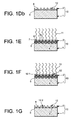
Plusieurs phénomènes peuvent se produire en fonction de la durée de l'irradiation. Si celle-ci est très brève, par exemple est délivrée par un laser femtoseconde, il se produit une ablation des implants 6 entraînant une exfoliation de la matière sus-jacente aux implants 6 sans échange significatif de chaleur. La nanostructuration 12 périodique est topographique comme illustré sur les figures 1Da, 1Db. C'est la faible durée de l'irradiation qui permet de limiter les effets thermiques.Several phenomena can occur depending on the duration of the irradiation. If it is very brief, for example is delivered by a femtosecond laser, there is
Il est ensuite possible de prévoir une étape de retrait de la matière exfoliée 20 qui pourrait se redéposer sur le substrat 10. En principe les implants 6 sont atomisés et donc disparaissent, cependant il se peut que seulement une partie de l'implant disparaisse entraînant l'exfoliation de ce qu'il y a dessus et laisse intact ce qu'il y a dessus, y compris une partie de l'implant.It is then possible to provide a step of removing the exfoliated
Ce retrait peut se faire par des techniques classiques en microélectronique telles que le brossage, le nettoyage chimique et/ou mégasonique.This removal can be done by conventional techniques in microelectronics such as brushing, chemical cleaning and / or megasonic.
On suppose que le substrat 10 représenté sur la figure 1Da est vu avant l'étape de nettoyage. Le résultat après nettoyage est représenté sur la figure 1Db.It is assumed that the
Il est possible de prévoir une étape de dépôt d'une couche sacrificielle 30 sur le substrat 10, du côté de sa face qui va être irradiée mais avant l'irradiation (figure 3A). Après l'irradiation, de la matière exfoliée 20 va retomber sur la couche sacrificielle 30. Par une étape de décollement (connue sous la dénomination anglo-saxonne de lift-off), on pourra retirer la couche sacrificielle 30 et la matière exfoliée 20 qui s'est déposée dessus. On obtiendra une configuration similaire à celle de la figure 1Db. Le matériau de la couche sacrificielle 30 peut par exemple être de l'oxyde de silicium.It is possible to provide a step of depositing a
Si l'irradiation se prolonge, les impulsions ayant une durée de l'ordre d'une ou quelques picosecondes ou nanosecondes, l'absorption localisée de l'onde électromagnétique par les implants 6 crée une augmentation de température au niveau des implants 6. Cette augmentation de température localisée est illustrée schématiquement sur la figure 1E par les cercles concentriques. La nanostructuration 12 surfacique peut être provoquée par la dilatation du matériau des implants 6 et/ou du matériau de la zone cristalline 4 qui entoure les implants 6 et en conséquence par la déformation du matériau sus-jacent aux implants 6. La nanostructuration 12 est alors une nanostructuration topographique. Il se forme des saillies 12.1 face aux implants 6. Cette déformation se produit en premier, sur la face du substrat la plus proche des implants, dans l'exemple décrit côté film mince 2 parce que son épaisseur permet la propagation de cette déformation. Cette configuration est illustrée sur la figure 1F. La déformation peut notamment être plastique, c'est-à-dire permanente ou irréversible, elle subsiste après l'arrêt de l'irradiation avec l'onde électromagnétique 11.If the irradiation is prolonged, the pulses having a duration of the order of one or a few picoseconds or nanoseconds, the localized absorption of the electromagnetic wave by the
La déformation peut même conduire à une exfoliation du matériau sus-jacent aux implants 6 comme illustré sur la figure 1G. Il se forme alors des creux 12.2 face aux implants 6.The deformation may even lead to exfoliation of the material overlying the
L'augmentation de température est inhomogène au niveau des implants 6 et au niveau de la zone cristalline 4 entre les implants. Il se crée des zones plus affectées thermiquement 7 (c'est à dire des zones plus chaudes) avoisinant des zones moins affectées thermiquement 8 (c'est-à-dire des zones moins chaudes).The increase in temperature is inhomogeneous at the level of the
Ces zones sont représentées sur la figure 1E. Il est possible que les zones plus affectées thermiquement 7 et les zones 8 moins affectées thermiquement en surface forment à elles seules la nanostructuration surfacique périodique. Cette nanostructuration 12 est alors thermique et non plus topographique. Une étape de dépôt ou de gravure pourra avoir lieu directement à la surface du substrat 10 possédant cette nanostructuration thermique. Une étape de gravure est illustrée à la figure 3B décrite ultérieurement.These areas are shown in Figure 1E. It is possible that the more thermally affected
Une étape de dépôt peut se faire par jet moléculaire, la température en surface du substrat d'accueil 10 influence la façon dont les atomes du matériau cristallin déposé se répartissent. Le dépôt se fait avec des vitesses de croissance différentes en fonction de la température de la zone réceptrice. On obtient avec ce dépôt, une croissance de nanostructures 14 tel qu'illustré sur la figure 3E. Si on dépose un matériau sur la surface d'un substrat présentant une nanostructuration topographique, en fonction de l'affinité entre ce matériau et le matériau en surface du substrat, la matière viendra naturellement se localiser dans les creux s'il y a une grande affinité et sur les bosses, s'il y a peu d'affinité, affin de minimiser l'énergie du système.A deposition step may be by molecular jet, the surface temperature of the
Il est possible, en variante, de déposer sur le substrat 10, préalablement à l'irradiation, une couche 13 d'un matériau qui va conduire à la nanostructuration lorsque l'irradiation aura eu lieu comme illustré sur la figure 3C. Ce matériau peut être un matériau à changement de phase en fonction de la température tel que le GeSbTe (germanium antimoine tellure). Après l'irradiation, on obtiendra une juxtaposition de zones amorphes 13.1 et de zones cristallines 13.2 comme illustré sur la figure 3D. La localisation des zones amorphes dépend en fait de l'historique thermique de l'emplacement, de l'état de départ du matériau à changement de phase. En général, on obtient du matériau amorphe quand le refroidissement, après la montée en température, est rapide et du matériau cristallin quand le refroidissement est lent. On peut donc déposer par exemple la matériau à changement de phase sous forme cristalline, élever localement au niveau des implants 6 la température jusqu'à une température suffisante pour assurer la transition et descendre rapidement en température pour obtenir au niveau des implants des zones amorphes. D'autres configurations sont bien sûr possibles.It is possible, alternatively, to deposit on the
Avant et/ou pendant la croissance, le dépôt, l'attaque ou l'irradiation, il est possible de chauffer de manière homogène le substrat 10. Cela peut se faire dans un four, l'augmentation de température peut être comprise par exemple entre environ 100°C et 600°C. Cette augmentation de température s'effectue de manière globale. Les gradients locaux de température engendrés par l'irradiation s'ajoutent à la température obtenue par le chauffage homogène. Cette étape n'est pas représentable. Cette étape permet par exemple, dans le cas du matériau à changement de phase, de situer avant irradiation au voisinage de la température de transition du matériau. Elle permet également de favoriser l'attaque.Before and / or during the growth, deposition, etching or irradiation, it is possible to heat the
On va voir maintenant plus en détail un exemple de réalisation du procédé de l'invention en se référant aux figures 2A à 2E.We will now see in more detail an embodiment of the method of the invention with reference to Figures 2A to 2E.
On part d'un substrat 10 formé de deux éléments 1, 2 ayant chacun une face en matériau cristallin, ces faces étant assemblées par collage moléculaire en prévoyant un angle de décalage en rotation de 0,88° entre leurs réseaux cristallins et pas de désorientation en flexion. Le matériau cristallin de ces deux éléments peut être le même par exemple du silicium ou bien être différent. Ce substrat 10 peut être qualifié de « twisté » à cause de l'angle de désorientation en rotation souvent appelé angle de « twist ». On se réfère à la figure 2A qui montre le substrat « twisté » 10 doté du réseau ordonné de dislocations 3 au sein d'une zone cristalline 4 située au voisinage d'interface 5 de collage. On suppose, dans l'exemple décrit, que les faces cristallines des deux éléments 1, 2, sont en silicium. L'un des éléments 1 peut être un substrat en silicium massif et l'autre élément 2 un film mince. En variante, l'autre élément 2 pourra être plus épais au moins au moment de l'assemblage, il comportera du matériau cristallin sur sa face à assembler. Il pourra être composite comme illustré sur la figure 2A. On lui fera subir une étape d'amincissement pour ne garder qu'un film mince 2 dont l'épaisseur sera par exemple d'environ 10 nanomètres. L'amincissement pour ne conserver que le film mince 2 peut se faire tout de suite après l'assemblage ou bien ultérieurement après l'étape de réalisation des implants. Cette étape d'amincissement peut par exemple se faire rectification, par abrasion mécanique ou même par abrasion chimique.It starts from a
Du silicium peut être employé comme matériau cristallin pour l'un ou l'autre des éléments 1, 2. Il est bien sûr possible d'utiliser d'autres matériaux tels que les matériaux III-V comme l'arséniure de gallium, l'arséniure d'indium ou le nitrure d'aluminium, les matériaux II-VI comme que le tellure de cadmium ou le séléniure de zinc ou le germanium, le nitrure de gallium, le germanium-silicium SixGey, le carbure de silicium, le phosphure d'indium, le saphir, le quartz, les grenats, le diamant.Silicon can be used as a crystalline material for either
Pour réaliser les implants 6 au niveau des dislocations 3, on peut déposer en surface du substrat 10, de préférence du côté du film mince 2, une couche 19 de matériau métallique apte à diffuser dans le matériau du cristallin du film mince 2 jusqu'au réseau de dislocations 3 et capable d'absorber fortement une onde électromagnétique utilisée par la suite. Il peut s'agir d'un dépôt chimique en phase vapeur, d'un dépôt électrolytique ou d'une pulvérisation. On peut se référer à la figure 2B. Le dépôt pourrait tout à fait être réalisé du côté du substrat massif 1 dans la mesure où le matériau métallique déposé est capable de diffuser jusqu'au réseau de dislocations 3. Le matériau métallique employé peut être réalisé à base d'or mais d'autres matériaux conviennent également tel le titane, l'aluminium, le platine, le cuivre, le tungstène, le nickel, l'argent.To produce the
L'épaisseur de la couche 19 sera égale ou inférieure à environ 15 nanomètres s'il s'agit d'or. On fait ensuite diffuser thermiquement le matériau métallique déposé dans le matériau cristallin de la zone cristalline 4 pour qu'il atteigne les dislocations 6 au moyen de l'application d'un budget thermique avec une température comprise entre environ 100°C et 1000°C, et par exemple de l'ordre de 500°C pendant un laps de temps compris entre environ 1 minute et 10 heures, par exemple pendant 5 heures. En diffusant jusqu'aux dislocations 3, le matériau métallique forme les implants 6.The thickness of the
Après la diffusion du matériau métallique, on ôte ce qui reste de la couche 19 de matériau métallique en surface comme illustré sur la figure 2C. Ce retrait peut se faire par exemple, lorsqu'il s'agit d'or ou de platine, par une attaque chimique humide avec de l'eau régale. On rappelle que l'eau régale est un liquide très oxydant formé d'un mélange d'acides chlorhydrique et nitrique. Elle a la propriété d'attaquer l'or et tous les métaux de la famille du platine. Une attaque sèche de type ionique pourrait aussi être utilisée.After the diffusion of the metallic material, the remainder of the
En variante, les implants 6 peuvent aussi être obtenus en réalisant au moins une implantation ionique de l'espèce choisie pour les réaliser, suivie d'une diffusion thermique. L'implantation se fera de préférence du côté du film mince 2. L'espèce implantée peut être notamment choisie parmi l'or, le titane, l'aluminium, le cuivre, le platine, le tungstène, le nickel, l'argent ou des dopants du matériau du film mince 2 (dans l'exemple du silicium) comme par exemple, le bore, l'arsenic. Avantageusement il est possible d'étaler le profil d'implantation en effectuant plusieurs implantations successives à différentes énergies comme dans l'exemple de la figure 4 afin de répartir les contraintes dans la structure. Si l'on implantait trop au même endroit, cela pourrait rendre amorphe localement le matériau, ce qui n'est pas le but recherché. On a représenté sur cette figure cinq implantations d'or successives avec des énergies de 3 KeV, 5 KeV, 7 KeV, 10 KeV, 12 KeV. Le ou les profils d'implantation peuvent se situer moins profondément, au même niveau ou plus profondément que les dislocations 3. Une étape de traitement thermique permet ensuite de faire diffuser les espèces implantées qui naturellement viennent se localiser au niveau des dislocations pour former les implants. Pour ne pas multiplier le nombre de figures inutilement, la figure 2C peut tout à fait illustrer les implants 6 obtenus par implantation ionique.Alternatively, the
On irradie par la suite, comme illustré à la figure 2D, le substrat 10 à partir de l'une de ses faces principales avec l'onde électromagnétique 11 pulsée dont la durée d'impulsion peut être plus ou moins longue.Subsequently, as shown in FIG. 2D, the
En utilisant une onde électromagnétique continue ou pulsée de grande durée d'impulsion (de l'ordre d'une ou quelques nanosecondes), l'absorption de l'énergie du laser puis la relaxation de cette énergie au sein des matériaux des implants et cristallin se feront par des processus classiques d'absorption puis de relaxation électrons-phonons sur des échelles de temps de l'ordre de la picoseconde, connus sous l'appellation générique "d'effets thermiques". Ces effets thermiques conduisent à une augmentation de la température, pouvant atteindre la température de vaporisation du matériau des implants voire du matériau cristallin. Cette vaporisation du matériau peut intervenir sur des échelles de temps de quelques nanosecondes, dépendant des propriétés physiques et optiques du matériau irradié et des caractéristiques du faisceau laser utilisé. Du fait de la différence de nature entre les implants et le matériau cristallin entre ces implants, des gradients de température pourront être localisés à la surface. La nanostructuration de la surface peut être induite par ces gradients de température ou par la vaporisation des implants. Du fait de la diffusion de la chaleur à la surface du matériau, il est avantageux d'avoir une distance importante entre les implants afin de distinguer en surface les zones thermiquement affectées des zones moins thermiquement affectées. Cette distance est typiquement comprise entre environ 0,1 à 1 micromètre.By using a continuous or pulsed electromagnetic wave of long pulse duration (of the order of one or a few nanoseconds), the absorption of the energy of the laser and the relaxation of this energy within the implants and crystalline materials will be done by classical processes of absorption and relaxation of electrons-phonons on time scales of the order of one picosecond, known generically as "thermal effects". These thermal effects lead to an increase in temperature, which can reach the vaporization temperature of the material of the implants or even the crystalline material. This vaporization of the material can occur on time scales of a few nanoseconds, depending on the physical and optical properties of the irradiated material and the characteristics of the laser beam used. Due to the difference in nature between the implants and the crystalline material between these implants, temperature gradients may be localized to the surface. Nanostructuring of the surface can be induced by these temperature gradients or by the vaporization of the implants. Due to the diffusion of heat to the surface of the material, it is advantageous to have a large distance between the implants in order to distinguish on the surface of the thermally affected areas of the less heat-affected areas. This distance is typically between about 0.1 to 1 micrometer.
En utilisant des impulsions de durée ultra brève (de l'ordre d'une ou quelques femtosecondes, voire d'une ou quelques picosecondes), l'énergie du laser sera absorbée, dans le cas des implants métalliques, par les électrons libres, tandis que pour le matériau cristallin semi-conducteur entre les implants, les électrons seront excités à partir de la bande de valence, ce qui nécessite que l'énergie des photons du laser soit supérieure au gap d'énergie entre la bande de valence et la bande de conduction du matériau cristallin. Suite à l'irradiation de la surface par le laser de durée d'impulsion ultra brève, en particulier en utilisant des densités de puissance pas trop élevées, pour lesquelles des porteurs libres ne pourront pas être créés au sein du matériau cristallin semi-conducteur entre les implants 6 par des processus de photo-ionisation ou d'ionisation par impact électron-électron, des électrons chauds, c'est à dire un plasma électronique, seront créés dans les implants 6, ce qui conduira à une ablation préférentielle de ces implants 6, là où la densité de porteurs libres est la plus élevée et donc à l'exfoliation des zones cristallines sus-jacente au implants 6. En fonction de la densité de puissance du faisceau laser, le plasma pourra être créé, préférentiellement dans la zone où résultera une densité importante d'électrons libres, à la suite de l'apparition d'une densité de charges importante qui induira une avalanche d'ionisation puis un claquage. Les électrons seront portés à très haute température par l'absorption de l'onde électromagnétique de durée ultra-brève, en comparaison du réseau cristallin beaucoup moins absorbant sur ces échelles de temps. Cela pourra conduire à la formation d'une onde de choc des électrons chauds et donc à l'éjection de matière localisée dans les zones où l'onde électromagnétique aura été préférentiellement absorbée. Il est à noter que cette technique permet de minimiser le couplage entre les électrons et les phonons du substrat. Il n'y donc pas ou peu d'élévation de la température moyenne du substrat semi-conducteur.By using pulses of ultra-short duration (of the order of one or a few femtoseconds, or even one or a few picoseconds), the energy of the laser will be absorbed, in the case of metal implants, by the free electrons, while that for the semiconductor crystalline material between the implants, the electrons will be excited from the valence band, which requires that the photon energy of the laser be greater than the energy gap between the valence band and the band of conduction of the crystalline material. Following the irradiation of the surface by the ultrashort pulse duration laser, in particular by using not too high power densities, for which free carriers can not be created within the crystalline semiconductor material between
On obtient alors une nanostructuration 12 surfacique qui possède la même période et la même symétrie que celles du réseau de dislocations 3 du substrat 10 avant traitement. Cette nanostructuration 12 qui est topographique est illustrée en figure 2E, elle possède des creux 12.2 face aux implants 6. Elle correspond au cas où l'irradiation a été menée avec des impulsions très brèves.
On peut par exemple déposer une couche d'oxyde de silicium 30 en surface du substrat 10, après la réalisation des implants 6 mais avant l'irradiation comme illustré à la figure 3A. Une fois l'irradiation appliquée et l'exfoliation obtenue, les creux 12.2 sont sans oxyde mais il reste des zones revêtues d'oxyde 12.3. Par gravure par exemple à l'aide d'une solution à base de TMAH, on peut accentuer le relief des creux 12.2 obtenus vis-à-vis des zones revêtues d'oxyde 12.3 qui elles ne sont pas attaquées comme illustré à la figure 3B. On obtient alors des zones revêtues d'oxyde 12.3 séparées par les creux 12.2. L'oxyde peut être éliminé comme évoqué plus haut surtout si lors de l'irradiation de la matière exfoliée s'est déposée sur les zones revêtues d'oxyde 12.3.For example, a
Le procédé de réalisation de la nanostructration qui vient d'être décrit peut avoir lieu sous atmosphère contrôlée par exemple à base de vide, d'oxygène O2, d'azote N2, d'argon Ar, d'hélium He, d'hydrogène H2 ou au sein d'un liquide tel que de l'eau ou tout autre liquide qui n'absorbe pas la longueur d'onde du laser. Cela permet, par exemple, de favoriser l'attaque, de contrôler l'exfoliation.The process for producing the nanostructration that has just been described can take place under a controlled atmosphere, for example based on vacuum, oxygen O 2 , nitrogen N 2 , argon Ar, helium He, hydrogen H 2 or in a liquid such as water or any other liquid that does not absorb the wavelength of the laser. This allows, for example, to promote the attack, to control the exfoliation.
Bien que plusieurs modes de réalisation de la présente invention aient été représentés et décrits de façon détaillée, on comprendra que différents changements et modifications puissent être apportés sans sortir du cadre de l'invention. Ces différentes possibilités (variantes) doivent être comprises comme n'étant pas exclusives les unes des autres.Although several embodiments of the present invention have been shown and described in detail, it will be understood that various changes and modifications can be made without departing from the scope of the invention. These different possibilities (variants) must be understood as not being exclusive of each other.
Claims (25)
Applications Claiming Priority (1)
| Application Number | Priority Date | Filing Date | Title |
|---|---|---|---|
| FR0652981A FR2903810B1 (en) | 2006-07-13 | 2006-07-13 | METHOD FOR NANOSTRUCTURING THE SURFACE OF A SUBSTRATE |
Publications (2)
| Publication Number | Publication Date |
|---|---|
| EP1878694A2 true EP1878694A2 (en) | 2008-01-16 |
| EP1878694A3 EP1878694A3 (en) | 2008-12-17 |
Family
ID=37688477
Family Applications (1)
| Application Number | Title | Priority Date | Filing Date |
|---|---|---|---|
| EP07112226A Withdrawn EP1878694A3 (en) | 2006-07-13 | 2007-07-11 | Method of nanostructuring the surface of a substrate |
Country Status (4)
| Country | Link |
|---|---|
| US (1) | US7655578B2 (en) |
| EP (1) | EP1878694A3 (en) |
| JP (1) | JP2008034843A (en) |
| FR (1) | FR2903810B1 (en) |
Families Citing this family (3)
| Publication number | Priority date | Publication date | Assignee | Title |
|---|---|---|---|---|
| FR2982853B1 (en) * | 2011-11-22 | 2018-01-12 | Ecole Polytechnique | METHOD FOR MANUFACTURING GRAPHENE FILM |
| JP6819093B2 (en) * | 2016-06-29 | 2021-01-27 | 株式会社Ihi | Material manufacturing equipment and material manufacturing method |
| CN109326712B (en) * | 2018-10-23 | 2023-03-21 | 京东方科技集团股份有限公司 | Preparation method of flexible substrate, flexible substrate and display panel |
Citations (2)
| Publication number | Priority date | Publication date | Assignee | Title |
|---|---|---|---|---|
| FR2766620A1 (en) * | 1997-07-22 | 1999-01-29 | Commissariat Energie Atomique | PRODUCTION OF MICROSTRUCTURES OR NANOSTRUCTURES ON A SUPPORT |
| WO2002029876A1 (en) * | 2000-10-06 | 2002-04-11 | Commissariat A L'energie Atomique | Method for revealing crystalline defects and/or stress field defects at the molecular adhesion interface of two solid materials |
Family Cites Families (8)
| Publication number | Priority date | Publication date | Assignee | Title |
|---|---|---|---|---|
| FR2819099B1 (en) | 2000-12-28 | 2003-09-26 | Commissariat Energie Atomique | METHOD FOR PRODUCING A STACKED STRUCTURE |
| US6831017B1 (en) * | 2002-04-05 | 2004-12-14 | Integrated Nanosystems, Inc. | Catalyst patterning for nanowire devices |
| FR2839505B1 (en) * | 2002-05-07 | 2005-07-15 | Univ Claude Bernard Lyon | METHOD FOR MODIFYING THE PROPERTIES OF A THIN LAYER AND SUBSTRATE USING THE PROCESS |
| ITTO20030730A1 (en) * | 2003-09-23 | 2005-03-24 | Infm Istituto Naz Per La Fisi Ca Della Mater | PROCEDURE FOR THE MANUFACTURE OF COMPLEX THREE-DIMENSIONAL STRUCTURES ON A SUB-MICROMETRIC SCALE BY COMBINED TWO-RESIST LITHOGRAPHY. |
| KR100666564B1 (en) * | 2004-08-04 | 2007-01-09 | 삼성에스디아이 주식회사 | Method for fabricating thin film transistor |
| US7820064B2 (en) * | 2005-05-10 | 2010-10-26 | The Regents Of The University Of California | Spinodally patterned nanostructures |
| US7276424B2 (en) * | 2005-06-29 | 2007-10-02 | Hewlett-Packard Development Company, L.P. | Fabrication of aligned nanowire lattices |
| FR2895419B1 (en) * | 2005-12-27 | 2008-02-22 | Commissariat Energie Atomique | PROCESS FOR SIMPLIFIED REALIZATION OF AN EPITAXIC STRUCTURE |
-
2006
- 2006-07-13 FR FR0652981A patent/FR2903810B1/en not_active Expired - Fee Related
-
2007
- 2007-07-03 US US11/773,082 patent/US7655578B2/en not_active Expired - Fee Related
- 2007-07-11 EP EP07112226A patent/EP1878694A3/en not_active Withdrawn
- 2007-07-12 JP JP2007183637A patent/JP2008034843A/en active Pending
Patent Citations (2)
| Publication number | Priority date | Publication date | Assignee | Title |
|---|---|---|---|---|
| FR2766620A1 (en) * | 1997-07-22 | 1999-01-29 | Commissariat Energie Atomique | PRODUCTION OF MICROSTRUCTURES OR NANOSTRUCTURES ON A SUPPORT |
| WO2002029876A1 (en) * | 2000-10-06 | 2002-04-11 | Commissariat A L'energie Atomique | Method for revealing crystalline defects and/or stress field defects at the molecular adhesion interface of two solid materials |
Non-Patent Citations (1)
| Title |
|---|
| LEE D M ET AL: "IMPURITY GETTERING BY MISFIT DISLOCATIONS IN SI (2% GE) EPITAXY: NICKEL" APPLIED PHYSICS LETTERS, AIP, AMERICAN INSTITUTE OF PHYSICS, MELVILLE, NY, US, vol. 53, no. 5, 1 août 1988 (1988-08-01), pages 370-372, XP000020101 ISSN: 0003-6951 * |
Also Published As
| Publication number | Publication date |
|---|---|
| FR2903810A1 (en) | 2008-01-18 |
| US20080280419A1 (en) | 2008-11-13 |
| US7655578B2 (en) | 2010-02-02 |
| EP1878694A3 (en) | 2008-12-17 |
| FR2903810B1 (en) | 2008-10-10 |
| JP2008034843A (en) | 2008-02-14 |
Similar Documents
| Publication | Publication Date | Title |
|---|---|---|
| EP0801419B1 (en) | Process of making a thin semiconductor film comprising electronic devices | |
| EP1285461B1 (en) | Method of manufacturing a thin film | |
| EP0660140B1 (en) | Method for making a relief structure on a substrate from semiconductor material | |
| EP2237698B1 (en) | Object provided with a graphics element transferred onto a support wafer and method of producing such an object | |
| EP3058583B1 (en) | Method for obtaining a wavy layer locally suspended on a substrate using a deformation by formation of wrinkles | |
| EP0994503B1 (en) | Process for manufacturing a structure comprising a thin layer composed of material containing conductive and isolation regions | |
| EP2468931B1 (en) | Method for cleaving a substrate and a substrate-structure assembly enabling this cleavage | |
| FR2978604A1 (en) | METHOD FOR THE HEALING OF DEFECTS IN A SEMICONDUCTOR LAYER | |
| EP2342744B1 (en) | Process for forming a single-crystal film in the microelectronics field | |
| EP1268884B1 (en) | Method and device for making substrates | |
| FR2896913A1 (en) | PROCESS FOR PRODUCING A QUASI-SUBSTRATE WAFER AND SEMICONDUCTOR BODY PRODUCED BY USING A QUASI-SUBSTRATE WAFER OF THIS TYPE | |
| WO2005064657A1 (en) | Method of sealing two plates with the formation of an ohmic contact therebetween | |
| WO2008031980A1 (en) | Method of transferring a layer at high temperature | |
| WO2004112125A1 (en) | Method for production of a very thin layer with thinning by means of induced self-support | |
| EP1878694A2 (en) | Method of nanostructuring the surface of a substrate | |
| EP1337683B1 (en) | Method for automatic organisation of microstructures or nanostructures and related device obtained | |
| FR2924273A1 (en) | DEFORMATION MODERATION METHOD | |
| FR2858461A1 (en) | IMPLEMENTING A STRUCTURE COMPRISING A PROTECTIVE LAYER AGAINST CHEMICAL TREATMENTS | |
| WO2006100301A1 (en) | Method of producing a hetero-structure comprising at least one thick layer of semiconductor material | |
| WO2023151852A1 (en) | Method for transferring a thin film onto a support substrate | |
| FR3079657A1 (en) | DETACHABLE COMPOSITE STRUCTURE BY APPLYING A LUMINOUS FLOW, AND METHOD FOR SEPARATING SUCH A STRUCTURE | |
| FR3062398A1 (en) | PROCESS FOR PRODUCING A SUBSTRATE FOR GROWING A TWO-DIMENSIONAL FILM OF HEXAGONAL CRYSTALLINE STRUCTURE | |
| EP4060716A1 (en) | Method for modifying a state of stress of at least one semiconductor layer |
Legal Events
| Date | Code | Title | Description |
|---|---|---|---|
| PUAI | Public reference made under article 153(3) epc to a published international application that has entered the european phase |
Free format text: ORIGINAL CODE: 0009012 |
|
| AK | Designated contracting states |
Kind code of ref document: A2 Designated state(s): AT BE BG CH CY CZ DE DK EE ES FI FR GB GR HU IE IS IT LI LT LU LV MC MT NL PL PT RO SE SI SK TR |
|
| AX | Request for extension of the european patent |
Extension state: AL BA HR MK YU |
|
| PUAL | Search report despatched |
Free format text: ORIGINAL CODE: 0009013 |
|
| AK | Designated contracting states |
Kind code of ref document: A3 Designated state(s): AT BE BG CH CY CZ DE DK EE ES FI FR GB GR HU IE IS IT LI LT LU LV MC MT NL PL PT RO SE SI SK TR |
|
| AX | Request for extension of the european patent |
Extension state: AL BA HR MK RS |
|
| 17P | Request for examination filed |
Effective date: 20090605 |
|
| AKX | Designation fees paid |
Designated state(s): AT BE BG CH CY CZ DE DK EE ES FI FR GB GR HU IE IS IT LI LT LU LV MC MT NL PL PT RO SE SI SK TR |
|
| STAA | Information on the status of an ep patent application or granted ep patent |
Free format text: STATUS: THE APPLICATION IS DEEMED TO BE WITHDRAWN |
|
| 18D | Application deemed to be withdrawn |
Effective date: 20110201 |