EP1873878B1 - Surface-emitting type semiconductor laser - Google Patents
Surface-emitting type semiconductor laser Download PDFInfo
- Publication number
- EP1873878B1 EP1873878B1 EP07012566A EP07012566A EP1873878B1 EP 1873878 B1 EP1873878 B1 EP 1873878B1 EP 07012566 A EP07012566 A EP 07012566A EP 07012566 A EP07012566 A EP 07012566A EP 1873878 B1 EP1873878 B1 EP 1873878B1
- Authority
- EP
- European Patent Office
- Prior art keywords
- layer
- refractive index
- type semiconductor
- semiconductor laser
- emitting type
- Prior art date
- Legal status (The legal status is an assumption and is not a legal conclusion. Google has not performed a legal analysis and makes no representation as to the accuracy of the status listed.)
- Expired - Fee Related
Links
Images

Classifications
-
- H—ELECTRICITY
- H01—ELECTRIC ELEMENTS
- H01S—DEVICES USING THE PROCESS OF LIGHT AMPLIFICATION BY STIMULATED EMISSION OF RADIATION [LASER] TO AMPLIFY OR GENERATE LIGHT; DEVICES USING STIMULATED EMISSION OF ELECTROMAGNETIC RADIATION IN WAVE RANGES OTHER THAN OPTICAL
- H01S5/00—Semiconductor lasers
- H01S5/10—Construction or shape of the optical resonator, e.g. extended or external cavity, coupled cavities, bent-guide, varying width, thickness or composition of the active region
- H01S5/18—Surface-emitting [SE] lasers, e.g. having both horizontal and vertical cavities
- H01S5/183—Surface-emitting [SE] lasers, e.g. having both horizontal and vertical cavities having only vertical cavities, e.g. vertical cavity surface-emitting lasers [VCSEL]
- H01S5/18308—Surface-emitting [SE] lasers, e.g. having both horizontal and vertical cavities having only vertical cavities, e.g. vertical cavity surface-emitting lasers [VCSEL] having a special structure for lateral current or light confinement
- H01S5/18311—Surface-emitting [SE] lasers, e.g. having both horizontal and vertical cavities having only vertical cavities, e.g. vertical cavity surface-emitting lasers [VCSEL] having a special structure for lateral current or light confinement using selective oxidation
- H01S5/18313—Surface-emitting [SE] lasers, e.g. having both horizontal and vertical cavities having only vertical cavities, e.g. vertical cavity surface-emitting lasers [VCSEL] having a special structure for lateral current or light confinement using selective oxidation by oxidizing at least one of the DBR layers
-
- H—ELECTRICITY
- H01—ELECTRIC ELEMENTS
- H01S—DEVICES USING THE PROCESS OF LIGHT AMPLIFICATION BY STIMULATED EMISSION OF RADIATION [LASER] TO AMPLIFY OR GENERATE LIGHT; DEVICES USING STIMULATED EMISSION OF ELECTROMAGNETIC RADIATION IN WAVE RANGES OTHER THAN OPTICAL
- H01S5/00—Semiconductor lasers
- H01S5/10—Construction or shape of the optical resonator, e.g. extended or external cavity, coupled cavities, bent-guide, varying width, thickness or composition of the active region
- H01S5/18—Surface-emitting [SE] lasers, e.g. having both horizontal and vertical cavities
- H01S5/183—Surface-emitting [SE] lasers, e.g. having both horizontal and vertical cavities having only vertical cavities, e.g. vertical cavity surface-emitting lasers [VCSEL]
- H01S5/18344—Surface-emitting [SE] lasers, e.g. having both horizontal and vertical cavities having only vertical cavities, e.g. vertical cavity surface-emitting lasers [VCSEL] characterized by the mesa, e.g. dimensions or shape of the mesa
- H01S5/18347—Mesa comprising active layer
-
- H—ELECTRICITY
- H01—ELECTRIC ELEMENTS
- H01S—DEVICES USING THE PROCESS OF LIGHT AMPLIFICATION BY STIMULATED EMISSION OF RADIATION [LASER] TO AMPLIFY OR GENERATE LIGHT; DEVICES USING STIMULATED EMISSION OF ELECTROMAGNETIC RADIATION IN WAVE RANGES OTHER THAN OPTICAL
- H01S2301/00—Functional characteristics
- H01S2301/16—Semiconductor lasers with special structural design to influence the modes, e.g. specific multimode
- H01S2301/166—Single transverse or lateral mode
-
- H—ELECTRICITY
- H01—ELECTRIC ELEMENTS
- H01S—DEVICES USING THE PROCESS OF LIGHT AMPLIFICATION BY STIMULATED EMISSION OF RADIATION [LASER] TO AMPLIFY OR GENERATE LIGHT; DEVICES USING STIMULATED EMISSION OF ELECTROMAGNETIC RADIATION IN WAVE RANGES OTHER THAN OPTICAL
- H01S2301/00—Functional characteristics
- H01S2301/18—Semiconductor lasers with special structural design for influencing the near- or far-field
-
- H—ELECTRICITY
- H01—ELECTRIC ELEMENTS
- H01S—DEVICES USING THE PROCESS OF LIGHT AMPLIFICATION BY STIMULATED EMISSION OF RADIATION [LASER] TO AMPLIFY OR GENERATE LIGHT; DEVICES USING STIMULATED EMISSION OF ELECTROMAGNETIC RADIATION IN WAVE RANGES OTHER THAN OPTICAL
- H01S5/00—Semiconductor lasers
- H01S5/10—Construction or shape of the optical resonator, e.g. extended or external cavity, coupled cavities, bent-guide, varying width, thickness or composition of the active region
- H01S5/18—Surface-emitting [SE] lasers, e.g. having both horizontal and vertical cavities
- H01S5/183—Surface-emitting [SE] lasers, e.g. having both horizontal and vertical cavities having only vertical cavities, e.g. vertical cavity surface-emitting lasers [VCSEL]
- H01S5/18344—Surface-emitting [SE] lasers, e.g. having both horizontal and vertical cavities having only vertical cavities, e.g. vertical cavity surface-emitting lasers [VCSEL] characterized by the mesa, e.g. dimensions or shape of the mesa
Definitions
- the present invention relates to surface-emitting type semiconductor lasers.
- the number of oscillation modes of surface-emitting type semiconductor lasers may be reduced by reducing the aperture diameter of the oxidized constricting layer.
- the output of a semiconductor laser increases with an increase in the current value injected, and reaches a maximum value (i.e., a rolloff point) at a certain current value.
- a maximum value i.e., a rolloff point
- the output of a semiconductor laser increases with an increase in the current value injected, and reaches a maximum value (i.e., a rolloff point) at a certain current value.
- Japanese laid-open patent application JP-A-2003-86895 describes a method in which a groove reaching the current constricting section is formed around the light emitting section, and an electrode is formed directly over the groove. As a result, the distance between a heat generating section and the electrode is shortened, thereby improving the heat radiation efficiency.
- the formulae (1) and (2) of claim 1 are satisfied.
- an energy increasing rate of a higher order resonance mode component can be reduced while scarcely reducing an energy increasing rate of a lower order resonance mode component among light that resonates in the active layer (hereafter referred to as "resonance light"), without regard to the thickness or the diameter of the current constricting layer.
- resonance light of higher order resonance mode components would be prevented from being laser-oscillated, without reducing the output of the surface-emitting type semiconductor laser, compared to a case where the aperture diameter of the current constricting layer is simply reduced.
- the design wavelength is a wavelength of light having the maximum intensity among light generated by the surface-emitting type semiconductor laser.
- the case of "a pair of a lower refractive index layer and a higher refractive index layer laminated in a thickness direction” includes a case in which another layer is laminated between the lower refractive index layer and the higher refractive index layer.
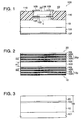
- the surface-emitting type semiconductor laser 100 may include, as shown in FIG. 1 , a substrate 101, a lower mirror 10, an active layer 103, an upper mirror 20, a dielectric layer 110, a first electrode 107 and a second electrode 109.
- the substrate 101 may be formed from, for example, a first conductivity type (for example, n-type) GaAs substrate.
- the lower mirror layer 10 of, for example, the first conductivity type is formed on the substrate 101.
- the lower mirror 10 is a multilayer mirror in which unit multilayer films 10p are laminated in plurality.
- Each of the unit multilayer films 10p may be composed of, for example, a lower refractive index layer 10L and a higher refractive index layer 10H formed below the lower refractive index layer 10L, as shown in FIG. 2 .
- the lower mirror 10 may be composed of, for example, a distributed Bragg reflection type (DBR) mirror of alternately laminated lower refractive index layers 10L and higher refractive index layers 10H.
- DBR distributed Bragg reflection type
- the lower refractive index layer 10L may be composed of, for example, an n-type Al 0.9 Ga 0.1 As layer (having a refractive index of 3.049).
- the higher refractive index layer 10H may be composed of, for example, an n-type Al 0.15 Ga 0.85 As layer (having a refractive index of 3.525).
- the number of the unit multilayer films 10p (the number of the pairs) may be, for example, 35.5 pairs to 43.5 pairs. It is noted that, as the unit multilayer films 10p of the lower mirror 10, any layers can be used if the layers compose the lower mirror 10 through repeating the layer structure of the unit multilayer films 10p.
- the unit multilayer film 10p may be composed of a lower refractive index layer 10L and a higher refractive index layer 10H formed on the lower refractive index layer 10L.
- the active layer 103 is formed on the lower mirror 10.
- the active layer 103 has a multiple quantum well (MQW) structure in which quantum well structures each formed from, for example, a GaAs well layer and an Al 0.2 Ga 0.8 As barrier layer are laminated in three layers.
- MQW multiple quantum well
- the upper mirror layer 20 of, for example, a second conductivity type (for example, p-type) is formed on the active layer 103.
- the upper mirror 20 is a multilayer mirror in which unit multilayer films 20p are laminated in plurality.
- Each of the unit multilayer films 20p may be composed of, for example, a lower refractive index layer 20L and a higher refractive index layer 20H formed below the lower refractive index layer 20L, as shown in FIG. 2 .
- the upper mirror 20 may be composed of, for example, a DBR mirror of alternately laminated lower refractive index layers 20L and higher refractive index layers 20H.
- the lower refractive index layer 20L may be composed of, for example, a p-type Al 0.9 Ga 0.1 As layer (having a refractive index of 3.049).
- the higher refractive index layer 20H may be composed of, for example, a p-type Al 0.15 Ga 0.85 As layer (having a refractive index of 3.525).
- the number of the unit multilayer films 20p (the number of the pairs) may be, for example, 19 pairs to 31 pairs. It is noted that, as the unit multilayer films 20p of the upper mirror 20, any layers can be used if the layers compose the upper mirror 20 through repeating the layer structure of the unit multilayer films 20p.
- the unit multilayer film 20p may be composed of a lower refractive index layer 20L and a higher refractive index layer 20H formed on the lower refractive index layer 20L.
- each of the plurality of unit multilayer films 10p and 20p described above may satisfy a formula (1) below.
- the active layer 103 satisfies a formula (2) below.
- ⁇ is a design wavelength of the surface-emitting type semiconductor laser 100
- m is a positive integer
- d D is a thickness of the unit multilayer film 10p
- 20p n D is a mean refractive index of the unit multilayer film 10p
- 20p is a thickness of the active layer 103
- n A is a means refractive index of the active layer 103.
- the lower limit value of d D and the upper limit value of d A may be decided depending on whether ⁇ is in a reflection band of the multilayer film mirrors (the lower mirror 10 and the upper mirror 20).
- the upper limit value of d A may be appropriately decided according to the design wavelength ⁇ , and may be a value that is greater by, for example, about 20% than the value of m ⁇ /2n A .
- the ratio (d A / d D ) between the thickness d A of the active layer 103 and the thickness d D of the unit multilayer film 10p, 20p may satisfy a formula (B) below.
- the design wavelength ⁇ may be, for example, 780 nm, 850 nm, 1300 nm or the like, without any particular limitation. Also, when m is, for example, 2, a 1 ⁇ resonator is formed, but m is not particularly limited.
- the thickness of each of the plural unit multilayer films 10p in the lower mirror 10 and the thickness of each of the plural unit multilayer films 20p in the upper mirror 20 may be the same d D .
- a mean refractive index of each of the plural unit multilayer films 10p in the lower mirror 10 and a mean refractive index of each of the plural unit multilayer films 20p in the upper mirror 20 may be the same n D .
- At least two pluralities of unit multilayer films 10p among the plural unit multilayer films 10p in the lower mirror 10 may have mutually different thicknesses.
- at least two pluralities of unit multilayer films 10p among the plural unit multilayer films 10p in the lower mirror 10 may have mutually different mean refractive indexes.
- at least two pluralities of unit multilayer films 20p among the plural unit multilayer films 20p in the upper mirror 20 may have mutually different thicknesses and/or mutually different mean refractive indexes.
- the formula (1) described above may be satisfied by at least one of the plural unit multilayer films 10p, 20p in the lower mirror 10 and the upper mirror 20.
- those of the unit multilayer films 10p, 20p that do not satisfy the formula (1) described above may satisfy a formula (3) below.
- d H is a thickness of the lower refractive index layer film
- d L is a thickness of the higher refractive index layer
- n L is a refractive index of the lower refractive index layer
- n H is a refractive index of the higher refractive index layer
- the number of laminated unit multilayer films 10p in the lower mirror 10, and the number of laminated unit multilayer films 20p in the upper mirror 20 may be appropriately adjusted, whereby the threshold value of the surface-emitting type semiconductor laser 100 can be adjusted.
- the lower mirror 10, the active layer 103 and the upper mirror 20 can form a vertical resonator. It is noted that the composition of each of the layers and the number of the layers composing the lower mirror 10, the active layer 103 and the upper mirror 20 may be appropriately adjusted depending on the requirements.
- the p-type upper mirror 20, the active layer 103 that is not doped with an impurity and the n-type lower mirror 10 form a pin diode.
- the upper mirror 20, the active layer 103 and a portion of the lower mirror 10 may form, for example, a columnar semiconductor laminate (hereafter referred to as a "columnar section") 30.
- the columnar section 30 has a plane configuration of, for example, a circular shape.
- At least one of the layers composing the upper mirror 20 can be formed as a current constricting layer 105.
- the current constricting layer 105 is formed in a region near the active layer 103.
- As the current constricting layer 105 for example, an AlGaAs layer that is oxidized or implanted with protons can be used.
- the current constricting layer 105 is a dielectric layer having an opening section.
- the current constricting layer 105 is formed in a ring shape.
- the first electrode 107 is formed on the back surface of the substrate 101, i.e., on the surface on the substrate side opposite to that on which the lower mirror 10 is formed.
- the first electrode 107 is electrically connected to the lower mirror 10 through the substrate 101.
- the first electrode 107 may be formed, for example, on the top surface of the lower mirror 10.
- the second electrode 109 is formed on the upper mirror 20 and the dielectric layer 110.
- the second electrode 109 is electrically connected to the upper mirror 20.
- the second electrode 109 has an opening section on the columnar section 30.
- the opening section forms a region where the second electrode 109 is not provided on the top surface of the upper mirror 20. This region defines a laser light emission surface 108.
- the emission surface 108 has a plane configuration of, for example, a circular shape.
- the dielectric layer 110 is formed on the lower mirror 10.
- the dielectric layer 110 is formed in a manner to surround the columnar section 30.
- the dielectric layer 110 can electrically isolate the second electrode 109 from the lower mirror 10.
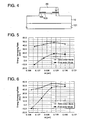
- FIG. 3 and FIG. 4 are cross-sectional views schematically showing steps of a manufacturing process for manufacturing the surface-emitting type semiconductor laser 100 in accordance with the present embodiment shown in FIG. 1 .
- an optical simulation on the surface-emitting type semiconductor laser 100 in accordance with the present embodiment was conducted, using the Finite-Difference Time-Domain method (FDTD method).
- the simulation was conducted on six samples (Nos. 1- 6).
- the samples to which numerical calculation was applied have the following structure.
- the substrate 101 an n-type GaAs substrate (with a refractive index of 3.62)
- the unit multilayer film 10p of the lower mirror 10 a film having a two-layer structure composed of an n-type Al 0.9 Ga 0.1 As layer (having a refractive index of 3.049), and an n-type Al 0.15 Ga 0.85 As layer (having a refractive index of 3.525).
- the active layer 103 a layer having a triple QW structure in which three layers of a quantum well structure each formed from a GaAs well layer (having a refractive index of 3.6201) and an Al 0.2 Ga 0.8 As barrier layer (having a refractive index of 3.4297) are laminated upon each other
- the mean refractive index n A of the active layer 103 3.3838
- the unit multilayer film 20p of the upper mirror 20 a film having a two-layer structure composed of a p-type Al 0.9 Ga 0.1 As layer (having a refractive index of 3.049), and a p-type Al 0.15 Ga 0.85 As layer (having a refractive index of 3.525)
- the dielectric layer 110 a layer of polyimide resin (having a refractive index of 1.78)
- the external atmosphere 40 of the surface-emitting type semiconductor laser 100 air (having a refractive index of 1.00)
- the inclination angle (the post inclination angle) ⁇ of the columnar section 30 80 degrees
- the outer diameter (the post diameter) of the columnar section 30 in a plan view i.e., the greatest diameter: about 50 ⁇ m
- the current constricting layer 105 an AlGaAs layer at the first layer on the active layer 103 that was oxidized (having a refractive index of 1.6)
- the aperture diameter of the current constricting layer 105 13 ⁇ m
- the thickness of the current constricting layer 105 12 nm, 30 nm
- the design wavelength ⁇ 850 nm
- the thicknesses of the layers composing each of the plural unit multilayer films 10p in the lower mirror 10 were decided to have the same ratio. More concretely, they were decided to be in reverse proportion to n H and n L . Also, the mean refractive index of each of the plural unit multilayer films 10p in the lower mirror 10, and the mean refractive index of each of the plural unit multilayer films 20p of in the upper mirror 20 were given the same n D .
- the thickness d D of the unit multilayer film 10p, 20p, the thickness d A of the active layer 103, the ratio of d A / d D , the number of pairs in the lower mirror 10, and the number of pairs in the upper mirror 20, in each of the numerical calculation samples (No. 1- No. 6) and the comparison examples, are shown in Table 1 and Table 2.
- Table 1 shows the cases where the thickness of the current constricting layer 105 was 12 nm
- Table 2 shows the cases where the thickness of the current constricting layer 105 was 30 nm.
- the values are presented in an effective number of digits that exceeds the grating cycle of AlGaAs, but they were used strictly for calculation, and would not present a particular problem if the values are used based on the real conditions.
- the thicknesses d D and d A were adjusted such that the design wavelength ⁇ was 850 nm.
- the number of pairs was calculated by calculating the life of photons using a one-dimensional FDTD method such that the mirror loss, that occurs when the thickness do of the unit multilayer film 10p, 20p is changed, would become equal in each of the samples. This was conducted only for maintaining the life of photons of the zero-order resonance mode component to be described below at about the same level, for comparison. Cases where the number of pairs is different from the present examples shall not depart from the invention. Table 1 No.
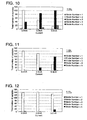
- FIG. 5 shows the case where the thickness of the current constricting layer 105 is 12 nm, and FIG.
- FIG. 6 shows the case where the thickness of the current constricting layer 105 is 30 nm.
- the thickness d D of the unit multilayer film 10p, 20p is plotted along the respective abscissa, and the active layer energy increasing rate is plotted along the respective ordinate.
- d D is made smaller (d A / d D is made greater)
- the energy increasing rate of resonance light of the first-order mode component changes to the negative, and goes into a state that does not arrive at laser oscillation.
- the first or higher-order resonance mode components do not arrive at laser oscillation (accordingly, the surface-emitting type semiconductor laser 100 does not emit light), and only the zero-order mode component resonance light causes laser oscillation (accordingly, the surface-emitting type semiconductor laser 100 emits light). Therefore, the laser light emitted from the surface-emitting type semiconductor laser 100 can be formed in a single mode. It is noted that, among resonance light, elimination of high-order resonance mode components (for example, the first-order mode component) is possible irrespective of the thickness of the current constricting layer 105, as indicated in FIG. 5 and FIG. 6 .
- the simulation was conducted with the zero-order mode component, among the resonance light, used as a lower order resonance mode component (hereafter referred to as the "lower order mode component"), and the first-order mode component as a higher order resonance mode component (hereafter referred to as the "higher order mode component”), but the present embodiment is not limited to them.
- a lower order mode component may be any mode component that has a lower order number than that of a higher order mode component. Accordingly, for example, as a lower order mode component, any one of the third or lower order resonance mode components may be used, and as a higher order mode component, any one of the fourth or higher order resonance mode components may be used.
- optical simulation on the surface-emitting type semiconductor laser 100 in accordance with the present embodiment was conducted, using the one-dimensional FDTD method, and its design was done in a manner such that the Q values (corresponding to the light confinement effect in a longitudinal direction due to the one-dimensional calculation) were generally at the same level.
- the threshold currents in other words, the current values that cause the lowest-order mode to oscillate can be set generally at the same level.
- the simulation was conducted for surface-emitting type semiconductor lasers with three conditions A-C. Samples to which the numerical calculation was applied have the following structure. Unless specifically noted otherwise, the samples have the same structure as that of the exemplary samples for numerical calculation described above.
- the unit multilayer film 10p of the lower mirror 10 a film having a two-layer structure composed of an n-type Al 0.9 Ga 0.1 As layer (having a refractive index of 3.049), and an n-type Al 0.12 Ga 0.88 As layer (having a refractive index of 3.544).
- the mean refractive index no of the unit multilayer film 10p of the lower mirror 10 2 n H n L /(n H + n L ) 3.278
- the active layer 103 a layer having a GRIN-SCH (graded-index, separate-confinement heterostructure) structure including a triple QW structure in which three layers of a quantum well structure each formed from a GaAs well layer (having a refractive index of 3.6201) and an Al 0.2 Ga 0.8 As barrier layer (having a refractive index of 3.4297) are laminated is sandwiched by upper and lower graded index layers composed of AlGaAs
- GRIN-SCH graded-index, separate-confinement heterostructure
- the mean refractive index n A of the active layer 103 3.3838
- the unit multilayer film 20p of the upper mirror 20 a film having a two-layer structure composed of a p-type Al 0.9 Ga 0.1 As layer (having a refractive index of 3.049), and a p-type Al 0.12 Ga 0.88 As layer (having a refractive index of 3.544)
- the aperture diameter (the diameter of the opening section) of the current constricting layer 105 4.5 ⁇ m, 6.0 ⁇ m
- the thickness of the current constricting layer 105 12 nm
- the total thickness d D of the unit multilayer film 10p, 20p, the details of d D i.e., the thickness of the higher refractive index layer 10H, 20H and the thickness of the lower refractive index layer 10L, 20L
- the thickness d A of the active layer 103 i.e., the thickness of the higher refractive index layer 10H, 20H and the thickness of the lower refractive index layer 10L, 20L
- the thickness d A of the active layer 103 i.e., the thickness of the higher refractive index layer 10H, 20H and the thickness of the lower refractive index layer 10L, 20L
- the thickness d A of the active layer 103 i.e., the thickness of the higher refractive index layer 10H, 20H and the thickness of the lower refractive index layer 10L, 20L
- the ratio of d A / d D between d A and d D in each of the samples (with the conditions A to C) and the comparison examples are shown in Table 3.
- the design wavelength, the number of pairs in the lower mirror 10, the number of pairs in the upper mirror 20, and Q values of the samples (with the conditions A to C) and the comparison samples are shown in Table 4.
- Table 6 shows mean values of threshold currents of the surface-emitting type semiconductor lasers. Table 6 Condition d A /d D Threshold Current [mA] Aperture Diameter of Current Constricting Layer 9.0 ⁇ m Aperture Diameter of Current Constricting Layer 12.0 ⁇ m A 1.05 r 0 0.308 0.421 B 1.10 r 0 0.423 0.479 C 1.15 r 0 0.393 0.425
- the threshold currents are about at the same level in both of the cases where the aperture diameter of the current constricting layer 105 is 4.5 ⁇ m and 6.0 ⁇ m. It is understood from this result that the currents that cause the lowest-order resonance mode component to oscillate can be set generally at the same level.
- FIG. 7 to FIG. 12 show the total number of samples whose mode number was 1, 2, 3, 4, and 5 or greater, respectively. It is noted that FIGS. 7 to 9 show the cases where the aperture diameter of the current constricting layer 105 is 4.5 ⁇ m, and FIGS. 10 to 12 show the cases where the aperture diameter of the current constricting layer 105 is 6.0 ⁇ m. Also, FIG. 7 and FIG. 10 show the cases with the condition A, FIG. 8 and FIG. 11 show the cases with the condition B, and FIG. 9 and FIG. 12 show the cases with the condition C.
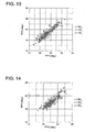
- FIG. 13 and 14 show radiation angles in perpendicularly traversing x-axis and y-axis (FFP x and FFP y , respectively). It is noted that FIG. 13 shows the case where the aperture diameter of the current constricting layer 105 is 4.5 ⁇ m, and FIG. 14 shows the case where the aperture diameter of the current constricting layer 105 is 6.0 ⁇ m.
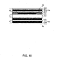
- FIG. 15 is a schematic cross-sectional view in part of a surface-emitting type semiconductor laser in accordance with the modified example.
- a unit multilayer film 10p in a lower mirror 10 may be composed of, for example, a lower refractive index layer 10L, a first graded index layer (hereafter referred to as a "first Gl layer”) 12 formed below the lower refractive index layer 10L, a higher refractive index layer 10H formed below the first Gl layer 12, and a second graded index layer (hereafter referred to as a "second Gl layer”) 14 formed below the higher refractive index layer 10H.
- the first Gl layer 12 for example, an AlGaAs layer with its Al composition continuously changing from 0.12 to 0.9 downwardly may be used.
- a unit multilayer film 20p in an upper mirror 20 may be composed of, for example, a lower refractive index layer 20L, a first GI layer 22 formed below the lower refractive index layer 20L, a higher refractive index layer 20H formed below the first GI layer 22, and a second GI layer 24 formed below the higher refractive index layer 20H.
- the energy increasing rate of resonance light of a higher order mode component can be reduced, while the energy increasing rate of resonance light of a lower order mode component is hardly reduced, irrespective of the thickness of the current constricting layer 105, the aperture diameter, and the inclination angle ⁇ of the post (the columnar section 30) and its largest outer diameter. This was also confirmed with the numerical calculation examples described above. As a result, laser oscillation of resonance light of high-order modes can be prevented from occurring, without reducing the output of the surface-emitting type semiconductor laser 100. Moreover, even when the output is increased, laser oscillation of resonance light of high-order modes can be prevented from occurring.
- the present embodiment it is possible to provide a surface-emitting type semiconductor laser which can reduce the number of oscillation modes of laser light, and can provide a higher output, compared to the case where the diameter of the current constricting layer is simply made smaller. It is noted that, when the aforementioned formulae (1) and (2) are satisfied, the effects of the surface-emitting type semiconductor laser 100 in accordance with the present embodiment can be obtained because of the following reasons.
- k z is a vertical direction component of the wavenumber vector within the resonator, and k // is a plane direction component thereof.
- k z and k // are decided to satisfy the continuity of electromagnetic field within the range that satisfies the total reflection condition at the boundary between the clad region including the current constricting layer 105 and the core region that does not include the current constricting layer 105.
- the values of k z and n eff k 0 are close to each other, such that k // has a small value, as is clear from the aforementioned formula. Accordingly, solutions of k // that satisfy the continuity of electromagnetic field described above, in other words, the number of transverse modes that can be allowed on the basis of the above formula is limited.
- the surface-emitting type semiconductor laser only those of the modes that satisfy the total reflection condition oscillate.
- k z is made even greater, whereby solutions of k // are further limited than the total reflection condition.
- k z can be made greater by reducing the thickness d D of the unit multilayer film 10p, 20p in the lower mirror 10 and the upper mirror 20.
- solutions of k // in this manner, the number of oscillation modes of laser light can be reduced.
- the wavelengths can be prevented from becoming shorter by making the thickness d A of the active layer 103 greater.
- d D smaller and d A greater, in other words, by making the thickness ratio d A / d D greater (more concretely, greater than mn D /n A ), the number of oscillation modes of laser light can be reduced, and laser oscillation can be made to occur at a desired design wavelength.
- the surface-emitting type semiconductor laser in accordance with the embodiment of the invention is applicable to, for example, a device having a waste heat structure, a device having a flip chip structure, a device having an electrostatic destruction (ESD) countermeasure structure, a device having a monitoring photodiode (MPD), a device having an ink jet microlens, a device having a dielectric mirror, an optical module such as an optical sub-assembly (OSA) using a CAN, a ceramic package or the like, an optical transmission apparatus implementing the aforementioned devices, and the like.
- ESD electrostatic destruction
- MPD monitoring photodiode
- OSA optical sub-assembly
- the substrate 101 in the surface-emitting type semiconductor laser 100 can be separated.
- the surface-emitting type semiconductor laser 100 may be provided without the substrate 101.
Description
- The present invention relates to surface-emitting type semiconductor lasers.
- With applications of surface-emitting type semiconductor lasers having expanded in recent years, it is desired further to reduce the number of oscillation modes of surface-emitting type semiconductor lasers while achieving a higher output. For example, in the case of a surface-emitting type semiconductor laser having an oxidized constriction layer, the number of oscillation modes may be reduced by reducing the aperture diameter of the oxidized constricting layer.
- It is noted that the output of a semiconductor laser increases with an increase in the current value injected, and reaches a maximum value (i.e., a rolloff point) at a certain current value. This is because, in a semiconductor laser, its gain spectrum shift with an increase in the device temperature which is caused by injection of current, and the gain reaches a maximum value at a certain temperature. When the aperture diameter of the oxidized constricting layer of the surface-emitting type semiconductor laser is relatively small, the temperature of the device would readily elevate, and its rolloff point is reached at a relatively low current value, such that a sufficient output may not be obtained. In this connection, in an attempt to prevent an increase in the device temperature,
Japanese laid-open patent application JP-A-2003-86895 - It is an object of the invention to provide a surface-emitting type semiconductor laser in which the number of oscillation modes of laser light can be reduced, and a higher output can be achieved, compared to a case where the aperture diameter of the current constricting layer is simply reduced.
- This object is achieved by a surface-emitting type semiconductor laser as claimed in
claim 1. Preferred embodiments of the invention are defined in the dependent claims. - In the surface-emitting type semiconductor laser in accordance with the present embodiment, the formulae (1) and (2) of
claim 1 are satisfied. By this, for example, an energy increasing rate of a higher order resonance mode component can be reduced while scarcely reducing an energy increasing rate of a lower order resonance mode component among light that resonates in the active layer (hereafter referred to as "resonance light"), without regard to the thickness or the diameter of the current constricting layer. This is also confirmed in a numerical calculation example to be described below. As a result, resonance light of higher order resonance mode components would be prevented from being laser-oscillated, without reducing the output of the surface-emitting type semiconductor laser, compared to a case where the aperture diameter of the current constricting layer is simply reduced. Therefore, in accordance with the present embodiment, it is possible to provide a surface-emitting type semiconductor laser that can reduce the number of oscillation modes of laser light, and provide a higher output, compared to a case where the aperture diameter of the current constricting layer is simply reduced. - It is noted that, in the invention, the design wavelength is a wavelength of light having the maximum intensity among light generated by the surface-emitting type semiconductor laser.
- It is noted that, in the present text where the term "above" is used in the context of the invention, for example, in a manner as "a certain member (hereafter referred to as 'B') formed 'above' another certain member (hereafter referred to as 'A')", the use of the term includes a case in which "B" is formed directly on "A," and a case in which "B" is formed over "A" through another member on "A."
- Also, in the present embodiment, the case of "a pair of a lower refractive index layer and a higher refractive index layer laminated in a thickness direction" includes a case in which another layer is laminated between the lower refractive index layer and the higher refractive index layer.
- Also, the notation λ /2nD expresses λ /(2nD).
- Preferred embodiments of the invention are described below with reference to the accompanying drawings, in which:
- FIG. 1
- is a schematic cross-sectional view of a surface-emitting type semiconductor laser in accordance with an embodiment of the invention;
- FIG. 2
- is a schematic cross-sectional view in part of the surface-emitting type semiconductor laser in accordance with the embodiment of the invention;
- FIG. 3
- is a view schematically showing a step of a method for manufacturing a surface-emitting type semiconductor laser in accordance with an embodiment of the invention;
- FIG.4
- is a view showing a step of the method for manufacturing a surface-emitting type semiconductor laser in accordance with the embodiment of the invention;
- FIG. 5
- is a graph showing calculation results of the energy increasing rate of resonance light at different modes in numerical calculation examples;
- FIG. 6
- is a graph showing calculation results of the energy increasing rate of resonance light at different modes in numerical calculation examples;
- FIG. 7
- is a graph showing the relation between the mode numbers and the sum of samples in experimental examples;
- FIG. 8
- is a graph showing the relation between the mode numbers and the sum of samples in experimental examples;
- FIG. 9
- is a graph showing the relation between the mode numbers and the sum of samples in experimental examples;
- FIG. 10
- is a graph showing the relation between the mode numbers and the sum of samples in experimental examples;
- FIG. 11
- is a graph showing the relation between the mode numbers and the sum of samples in experimental examples;
- FIG. 12
- is a graph showing the relation between the mode numbers and the sum of samples in experimental examples;
- FIG. 13
- is a graph showing radiation angles in two orthogonal axes in accordance with experimental examples;
- FIG. 14
- is a graph showing radiation angles in two orthogonal axes in accordance with experimental examples;
- FIG. 15
- is a schematic cross-sectional view of a surface-emitting type semiconductor laser in accordance with a modified example of the embodiment of the invention.
-
-
FIG. 1 is a schematic cross-sectional view of the surface-emittingtype semiconductor laser 100, and -
FIG. 2 is a schematic cross-sectional view in enlargement of a region V inFIG. 1 . - The surface-emitting
type semiconductor laser 100 may include, as shown inFIG. 1 , asubstrate 101, alower mirror 10, anactive layer 103, anupper mirror 20, adielectric layer 110, afirst electrode 107 and asecond electrode 109. - The
substrate 101 may be formed from, for example, a first conductivity type (for example, n-type) GaAs substrate. - The
lower mirror layer 10 of, for example, the first conductivity type is formed on thesubstrate 101. Thelower mirror 10 is a multilayer mirror in whichunit multilayer films 10p are laminated in plurality. Each of theunit multilayer films 10p may be composed of, for example, a lowerrefractive index layer 10L and a higherrefractive index layer 10H formed below the lowerrefractive index layer 10L, as shown inFIG. 2 . In other words, thelower mirror 10 may be composed of, for example, a distributed Bragg reflection type (DBR) mirror of alternately laminated lowerrefractive index layers 10L and higherrefractive index layers 10H. The lowerrefractive index layer 10L may be composed of, for example, an n-type Al0.9Ga0.1As layer (having a refractive index of 3.049). The higherrefractive index layer 10H may be composed of, for example, an n-type Al0.15Ga0.85As layer (having a refractive index of 3.525). The number of theunit multilayer films 10p (the number of the pairs) may be, for example, 35.5 pairs to 43.5 pairs. It is noted that, as theunit multilayer films 10p of thelower mirror 10, any layers can be used if the layers compose thelower mirror 10 through repeating the layer structure of theunit multilayer films 10p. For example, theunit multilayer film 10p may be composed of a lowerrefractive index layer 10L and a higherrefractive index layer 10H formed on the lowerrefractive index layer 10L. - The
active layer 103 is formed on thelower mirror 10. Theactive layer 103 has a multiple quantum well (MQW) structure in which quantum well structures each formed from, for example, a GaAs well layer and an Al0.2Ga0.8As barrier layer are laminated in three layers. - The
upper mirror layer 20 of, for example, a second conductivity type (for example, p-type) is formed on theactive layer 103. Theupper mirror 20 is a multilayer mirror in whichunit multilayer films 20p are laminated in plurality. Each of theunit multilayer films 20p may be composed of, for example, a lowerrefractive index layer 20L and a higherrefractive index layer 20H formed below the lowerrefractive index layer 20L, as shown inFIG. 2 . In other words, theupper mirror 20 may be composed of, for example, a DBR mirror of alternately laminated lower refractive index layers 20L and higher refractive index layers 20H. The lowerrefractive index layer 20L may be composed of, for example, a p-type Al0.9Ga0.1As layer (having a refractive index of 3.049). The higherrefractive index layer 20H may be composed of, for example, a p-type Al0.15Ga0.85As layer (having a refractive index of 3.525). The number of theunit multilayer films 20p (the number of the pairs) may be, for example, 19 pairs to 31 pairs. It is noted that, as theunit multilayer films 20p of theupper mirror 20, any layers can be used if the layers compose theupper mirror 20 through repeating the layer structure of theunit multilayer films 20p. For example, theunit multilayer film 20p may be composed of a lowerrefractive index layer 20L and a higherrefractive index layer 20H formed on the lowerrefractive index layer 20L. - In the present embodiment, for example, each of the plurality of
unit multilayer films active layer 103 satisfies a formula (2) below.

where λ is a design wavelength of the surface-emittingtype semiconductor laser 100,
m is a positive integer,
dD is a thickness of theunit multilayer film
nD is a mean refractive index of theunit multilayer film
dA is a thickness of theactive layer 103, and
nA is a means refractive index of theactive layer 103. - It is noted that the lower limit value of dD and the upper limit value of dA may be decided depending on whether λ is in a reflection band of the multilayer film mirrors (the
lower mirror 10 and the upper mirror 20). The lower limit value of dD may be a value that is smaller by, for example, about 5% than the value of λ /2nD in the case of a multilayer film mirror composed of AlxGa1-x As (x = 0.15, 0.90) with λ being 850 nm. Also, the upper limit value of dA may be appropriately decided according to the design wavelength λ, and may be a value that is greater by, for example, about 20% than the value of mλ /2nA. - Also, the above-described formulae (1) and (2) may be rewritten by a formula (A) below.

- Also, based on the formulae (1) and (2) described above, the ratio (dA / dD) between the thickness dA of the
active layer 103 and the thickness dD of theunit multilayer film 
- The design wavelength λ may be, for example, 780 nm, 850 nm, 1300 nm or the like, without any particular limitation. Also, when m is, for example, 2, a 1 λ resonator is formed, but m is not particularly limited.
- In the present embodiment, for example as shown in
FIG. 2 , the thickness of each of the pluralunit multilayer films 10p in thelower mirror 10 and the thickness of each of the pluralunit multilayer films 20p in theupper mirror 20 may be the same dD. Also, in accordance with the present embodiment, for example, a mean refractive index of each of the pluralunit multilayer films 10p in thelower mirror 10, and a mean refractive index of each of the pluralunit multilayer films 20p in theupper mirror 20 may be the same nD. - Also, for example, at least two pluralities of
unit multilayer films 10p among the pluralunit multilayer films 10p in thelower mirror 10 may have mutually different thicknesses. Also, for example, at least two pluralities ofunit multilayer films 10p among the pluralunit multilayer films 10p in thelower mirror 10 may have mutually different mean refractive indexes. Similarly, at least two pluralities ofunit multilayer films 20p among the pluralunit multilayer films 20p in theupper mirror 20 may have mutually different thicknesses and/or mutually different mean refractive indexes. The formula (1) described above may be satisfied by at least one of the pluralunit multilayer films lower mirror 10 and theupper mirror 20. For example, those of theunit multilayer films 
- Also, for example, as shown in
FIG. 2 , when theunit multilayer films 10p of thelower mirror 10 are composed of lower refractive index layers 10L and higher refractive index layers 10H, and theunit multilayer films 20p of theupper mirror 20 are composed of lower refractive index layers 20L and higher refractive index layers 20H, the formula (1) described above can be rewritten to a formula (4) below.
where dH is a thickness of the lower refractive index layer film,
dL is a thickness of the higher refractive index layer,
nL is a refractive index of the lower refractive index layer, and
nH is a refractive index of the higher refractive index layer. - Also, the number of laminated
unit multilayer films 10p in thelower mirror 10, and the number of laminatedunit multilayer films 20p in theupper mirror 20 may be appropriately adjusted, whereby the threshold value of the surface-emittingtype semiconductor laser 100 can be adjusted. - The
lower mirror 10, theactive layer 103 and theupper mirror 20 can form a vertical resonator. It is noted that the composition of each of the layers and the number of the layers composing thelower mirror 10, theactive layer 103 and theupper mirror 20 may be appropriately adjusted depending on the requirements. The p-typeupper mirror 20, theactive layer 103 that is not doped with an impurity and the n-typelower mirror 10 form a pin diode. Theupper mirror 20, theactive layer 103 and a portion of thelower mirror 10 may form, for example, a columnar semiconductor laminate (hereafter referred to as a "columnar section") 30. Thecolumnar section 30 has a plane configuration of, for example, a circular shape. - Also, as shown in
FIG. 1 , for example, at least one of the layers composing theupper mirror 20 can be formed as acurrent constricting layer 105. Thecurrent constricting layer 105 is formed in a region near theactive layer 103. As thecurrent constricting layer 105, for example, an AlGaAs layer that is oxidized or implanted with protons can be used. Thecurrent constricting layer 105 is a dielectric layer having an opening section. Thecurrent constricting layer 105 is formed in a ring shape. - The
first electrode 107 is formed on the back surface of thesubstrate 101, i.e., on the surface on the substrate side opposite to that on which thelower mirror 10 is formed. Thefirst electrode 107 is electrically connected to thelower mirror 10 through thesubstrate 101. Though not illustrated, thefirst electrode 107 may be formed, for example, on the top surface of thelower mirror 10. - The
second electrode 109 is formed on theupper mirror 20 and thedielectric layer 110. Thesecond electrode 109 is electrically connected to theupper mirror 20. Thesecond electrode 109 has an opening section on thecolumnar section 30. The opening section forms a region where thesecond electrode 109 is not provided on the top surface of theupper mirror 20. This region defines a laser light emission surface 108. The emission surface 108 has a plane configuration of, for example, a circular shape. - The
dielectric layer 110 is formed on thelower mirror 10. Thedielectric layer 110 is formed in a manner to surround thecolumnar section 30. Thedielectric layer 110 can electrically isolate thesecond electrode 109 from thelower mirror 10. -
FIG. 3 andFIG. 4 are cross-sectional views schematically showing steps of a manufacturing process for manufacturing the surface-emittingtype semiconductor laser 100 in accordance with the present embodiment shown inFIG. 1 . - (1) First, as shown in
FIG. 3 , for example, an n-type GaAs substrate is prepared as asubstrate 101. Then, asemiconductor multilayer film 150 is formed on thesubstrate 101 by epitaxial growth while modifying its composition. Thesemiconductor multilayer film 150 is formed by successively laminating semiconductor layers that compose alower mirror 10, anactive layer 103 and anupper mirror 20. When theupper mirror 20 is grown, at least one layer thereof near theactive layer 103 is formed to be a layer that is later oxidized and becomes thecurrent constricting layer 105. As the layer that is to become thecurrent constricting layer 105, for example, an AlGaAs layer with its Al composition being 0.95 or greater may be used. - (2) Then, as shown in
FIG. 4 , thesemiconductor multilayer film 150 is patterned, thereby forming alower mirror 10, anactive layer 103, and anupper mirror 20, each in a desired configuration. By this, thecolumnar section 30 is formed. Thesemiconductor multilayer film 150 may be patterned by using, for example, a lithography technique and an etching technique.
Then, by placing thesubstrate 101 on which thecolumnar section 30 is formed through the aforementioned steps in a water vapor atmosphere, for example, at about 400°C, the layer that is to become the aforementioned current constrictinglayer 105 is oxidized from its side surface, thereby forming thecurrent constricting layer 105. - (3) Next, as shown in
FIG. 1 , adielectric layer 110 is formed on thelower mirror 10 in a manner to surround thecolumnar section 30. First, a dielectric layer composed of polyimide resin or the like is formed over the entire surface by using, for example, a spin coat method. Then, the top surface of thecolumnar section 30 is exposed by using, for example, a CMP method or the like. Then, the dielectric layer is patterned by, for example, a lithography technique and an etching technique. In this manner, thedielectric layer 110 in a desired configuration can be formed.
Then, afirst electrode 107 and asecond electrode 109 are formed. The electrodes may be formed in desired configurations, respectively, by, for example, a combination of a vacuum vapor deposition method and a lift-off method, or the like. It is noted that the order of forming the electrodes is not particularly limited. - (4) By the steps described above, the surface-emitting
type semiconductor laser 100 in accordance with the present embodiment is obtained, as shown inFIG. 1 . - In the numerical calculation examples, an optical simulation on the surface-emitting
type semiconductor laser 100 in accordance with the present embodiment was conducted, using the Finite-Difference Time-Domain method (FDTD method). The simulation was conducted on six samples (Nos. 1- 6). The samples to which numerical calculation was applied have the following structure. - The substrate 101: an n-type GaAs substrate (with a refractive index of 3.62)
- The
unit multilayer film 10p of the lower mirror 10: a film having a two-layer structure composed of an n-type Al0.9Ga0.1As layer (having a refractive index of 3.049), and an n-type Al0.15Ga0.85As layer (having a refractive index of 3.525). - The mean refractive index no of the
unit multilayer film 10p of the lower mirror 10: 2 nH nL / (nH + nL) = 3.2697 - The active layer 103: a layer having a triple QW structure in which three layers of a quantum well structure each formed from a GaAs well layer (having a refractive index of 3.6201) and an Al0.2Ga0.8As barrier layer (having a refractive index of 3.4297) are laminated upon each other
- The mean refractive index nA of the active layer 103: 3.3838
- The
unit multilayer film 20p of the upper mirror 20: a film having a two-layer structure composed of a p-type Al0.9Ga0.1As layer (having a refractive index of 3.049), and a p-type Al0.15Ga0.85As layer (having a refractive index of 3.525) - The mean refractive index nD of the
unit multilayer film 20p of the upper mirror 20: 2nHnL / (nH + nL) = 3.2697 - The dielectric layer 110: a layer of polyimide resin (having a refractive index of 1.78)
- The
external atmosphere 40 of the surface-emitting type semiconductor laser 100: air (having a refractive index of 1.00) - The inclination angle (the post inclination angle) θ of the columnar section 30: 80 degrees
- The outer diameter (the post diameter) of the
columnar section 30 in a plan view (i.e., the greatest diameter): about 50 µm - The number of pairs in the
lower mirror 10 in the columnar section 30: 4 pairs - The current constricting layer 105: an AlGaAs layer at the first layer on the
active layer 103 that was oxidized (having a refractive index of 1.6) - The aperture diameter of the current constricting layer 105: 13 µm
- The thickness of the current constricting layer 105: 12 nm, 30 nm
- The design wavelength λ : 850 nm
- m in the above-described formula (2): 2
- In each of the samples of the numerical calculation examples, the thicknesses of the layers composing each of the plural
unit multilayer films 10p in thelower mirror 10, and the thicknesses of the layers composing each of the pluralunit multilayer films 20p in theupper mirror 20 were decided to have the same ratio. More concretely, they were decided to be in reverse proportion to nH and nL. Also, the mean refractive index of each of the pluralunit multilayer films 10p in thelower mirror 10, and the mean refractive index of each of the pluralunit multilayer films 20p of in theupper mirror 20 were given the same nD. - The ratio (dA /dD) between the thickness dA of the
active layer 103 and the thickness dD of theunit multilayer film - The thickness dD of the
unit multilayer film active layer 103, the ratio of dA / dD, the number of pairs in thelower mirror 10, and the number of pairs in theupper mirror 20, in each of the numerical calculation samples (No. 1- No. 6) and the comparison examples, are shown in Table 1 and Table 2. Table 1 shows the cases where the thickness of thecurrent constricting layer 105 was 12 nm, and Table 2 shows the cases where the thickness of thecurrent constricting layer 105 was 30 nm. The values are presented in an effective number of digits that exceeds the grating cycle of AlGaAs, but they were used strictly for calculation, and would not present a particular problem if the values are used based on the real conditions. The thicknesses dD and dA were adjusted such that the design wavelength λ was 850 nm. The thicknesses dD and dA in each of the numerical calculation samples (No. 1 - No. 6) satisfied the formulae (1) and (2) described above, with m=2 in the numerical calculation examples. - Also, the number of pairs was calculated by calculating the life of photons using a one-dimensional FDTD method such that the mirror loss, that occurs when the thickness do of the
unit multilayer film Table 1 No. dD [µm] dA [µm] dA / dD Number of Pairs in Lower Mirror Number of Pairs in Upper Mirror 1 0.12663 0.28144 1.9325 × 1.15 43.5 31 2 0.12766 0.27139 1.9325 × 1.10 37.5 28 3 0.12878 0.26132 1.9325 × 1.05 35.5 26 Comparison Example 0.12998 0.25119 1.9325 37.5 25 Table 2 No. dD [µm] dA [µm] dA / dD Number of Pairs in Lower Mirror Number of Pairs in Upper Mirror 4 0.12630 0.28070 1.9325 ×1.15 43.5 31 5 0.12741 0.27086 1.9325 ×1.10 37.5 28 6 0.12853 0.26080 1.9325 ×1.05 35.5 26 Comparison Example 0.12998 0.25119 1.9325 37.5 25 - Energy increasing rates of resonance light of the zero-order resonance mode component (hereafter referred to as the "zero-order mode component") and the first-order resonance mode component (hereafter referred to as the "first-order mode component") in the active layer were calculated for each of the numerical calculation samples (No. 1 - No. 6) and the comparison example, using the two-dimensional FDTD method, and the calculation results are shown in
FIG. 5 and FIG. 6 . It is noted that the calculation was conducted with a gain given to theactive layer 103, in the amount corresponding to that at the time of a current injection.FIG. 5 shows the case where the thickness of thecurrent constricting layer 105 is 12 nm, andFIG. 6 shows the case where the thickness of thecurrent constricting layer 105 is 30 nm. The thickness dD of theunit multilayer film FIG. 5 and FIG. 6 , when dD is made smaller (dA / dD is made greater), it is observed that the energy increasing rate of resonance light of the first-order mode component decreases, while the energy increasing rate of resonance light of the zero-order mode component scarcely changes. When dD is made smaller (dA / dD is made greater), it is observed that the energy increasing rate of resonance light of the first-order mode component changes to the negative, and goes into a state that does not arrive at laser oscillation. In other words, among the resonance light, the first or higher-order resonance mode components do not arrive at laser oscillation (accordingly, the surface-emittingtype semiconductor laser 100 does not emit light), and only the zero-order mode component resonance light causes laser oscillation (accordingly, the surface-emittingtype semiconductor laser 100 emits light). Therefore, the laser light emitted from the surface-emittingtype semiconductor laser 100 can be formed in a single mode. It is noted that, among resonance light, elimination of high-order resonance mode components (for example, the first-order mode component) is possible irrespective of the thickness of thecurrent constricting layer 105, as indicated inFIG. 5 and FIG. 6 . - In the numerical calculation examples described above, the simulation was conducted with the zero-order mode component, among the resonance light, used as a lower order resonance mode component (hereafter referred to as the "lower order mode component"), and the first-order mode component as a higher order resonance mode component (hereafter referred to as the "higher order mode component"), but the present embodiment is not limited to them. A lower order mode component may be any mode component that has a lower order number than that of a higher order mode component. Accordingly, for example, as a lower order mode component, any one of the third or lower order resonance mode components may be used, and as a higher order mode component, any one of the fourth or higher order resonance mode components may be used.
- In the experimental examples, optical simulation on the surface-emitting
type semiconductor laser 100 in accordance with the present embodiment was conducted, using the one-dimensional FDTD method, and its design was done in a manner such that the Q values (corresponding to the light confinement effect in a longitudinal direction due to the one-dimensional calculation) were generally at the same level. By setting the Q values generally at the same level, the threshold currents, in other words, the current values that cause the lowest-order mode to oscillate can be set generally at the same level. The simulation was conducted for surface-emitting type semiconductor lasers with three conditions A-C. Samples to which the numerical calculation was applied have the following structure. Unless specifically noted otherwise, the samples have the same structure as that of the exemplary samples for numerical calculation described above. - The
unit multilayer film 10p of the lower mirror 10: a film having a two-layer structure composed of an n-type Al0.9Ga0.1As layer (having a refractive index of 3.049), and an n-type Al0.12Ga0.88As layer (having a refractive index of 3.544). - The mean refractive index no of the
unit multilayer film 10p of the lower mirror 10: 2 nH nL /(nH + nL) 3.278 - The active layer 103: a layer having a GRIN-SCH (graded-index, separate-confinement heterostructure) structure including a triple QW structure in which three layers of a quantum well structure each formed from a GaAs well layer (having a refractive index of 3.6201) and an Al0.2Ga0.8As barrier layer (having a refractive index of 3.4297) are laminated is sandwiched by upper and lower graded index layers composed of AlGaAs
- The mean refractive index nA of the active layer 103: 3.3838
- The
unit multilayer film 20p of the upper mirror 20: a film having a two-layer structure composed of a p-type Al0.9Ga0.1As layer (having a refractive index of 3.049), and a p-type Al0.12Ga0.88As layer (having a refractive index of 3.544) - The mean refractive index nD of the
unit multilayer film 20p of the upper mirror 20: 2 nH nL (nH + nL) = 3.2697 - The aperture diameter (the diameter of the opening section) of the current constricting layer 105: 4.5 µm, 6.0 µm
- The thickness of the current constricting layer 105: 12 nm
- The ratio dA /dD between the thickness dA of the
active layer 103 and the thickness dD of theunit multilayer film - The total thickness dD of the
unit multilayer film refractive index layer refractive index layer active layer 103, and the ratio of dA / dD between dA and dD in each of the samples (with the conditions A to C) and the comparison examples, are shown in Table 3. The values are presented in an effective number of digits that exceeds the grating cycle of AlGaAs, but they were used strictly for calculation, and would not present a particular problem if the values are used based on the real conditions. The design wavelength, the number of pairs in thelower mirror 10, the number of pairs in theupper mirror 20, and Q values of the samples (with the conditions A to C) and the comparison samples are shown in Table 4. The thicknesses dD and dA in each of the samples (with the conditions A to C) satisfy the above-described formulae (1) and (2), with m = 2 in the numerical calculation examples.Table 3 Condition dD [nm] dA [nm] dA/dD Total Thickness Details Higher refractive index layer Lower refractive index layer Comparison Example 129.66 59.96 69.69 253.77 r0 = 1.96 A 127.64 59.03 68.61 263.34 1.05 r0 B 126.58 58.57 68.04 273.59 1.10 r0 C 125.53 58.05 67.48 283.67 1.15 r0 Table 4 Condition Design Wavelength [nm] The number of pairs in the lower mirror The number of pairs in the upper mirror Q value Comparison Example 853.3 40.5 23 15560 A 850.11 24 16040 B 850.14 25 14620 C 850.18 29 15400 - It is understood from Table 3 and Table 4 that they are designed in a manner that the Q values are generally at the same level in all of the conditions.
- Then, the samples described above (with the conditions A to C) were actually manufactured according to the design described above. 144 samples were manufactured. Mean values of oscillation wavelength (peak wavelength) of the surface-emitting type semiconductor lasers manufactured are shown in Table 5.
Table 5 Condition dA/dD Oscillation Wavelength [nm] Aperture Diameter of Current Constricting Layer 9.0 µm Aperture Diameter of Current Constricting Layer 12.0 µm A 1.05 r0 852.52 850.75 B 1.10 r0 853.93 851.87 C 1.15 r0 851.64 854.82 - As shown in Table 5, it is understood that the surface-emitting type semiconductor lasers manufactured oscillate at about the same wavelength in all of the conditions.
- Table 6 below shows mean values of threshold currents of the surface-emitting type semiconductor lasers.
Table 6 Condition dA/dD Threshold Current [mA] Aperture Diameter of Current Constricting Layer 9.0 µm Aperture Diameter of Current Constricting Layer 12.0 µm A 1.05 r0 0.308 0.421 B 1.10 r0 0.423 0.479 C 1.15 r0 0.393 0.425 - As shown in Table 6, it is understood that the threshold currents are about at the same level in both of the cases where the aperture diameter of the
current constricting layer 105 is 4.5 µm and 6.0 µm. It is understood from this result that the currents that cause the lowest-order resonance mode component to oscillate can be set generally at the same level. - Then, currents (3.0 mA, 4.0 mA and 5.0 mA) were injected in each of the samples (with the condition A to C), and the numbers of resonance mode components that oscillated (hereafter also referred to as the "mode number") were measured.
FIG. 7 to FIG. 12 show the total number of samples whose mode number was 1, 2, 3, 4, and 5 or greater, respectively. It is noted thatFIGS. 7 to 9 show the cases where the aperture diameter of thecurrent constricting layer 105 is 4.5 µm, andFIGS. 10 to 12 show the cases where the aperture diameter of thecurrent constricting layer 105 is 6.0 µm. Also,FIG. 7 andFIG. 10 show the cases with the condition A,FIG. 8 andFIG. 11 show the cases with the condition B, andFIG. 9 andFIG. 12 show the cases with the condition C. - It is observed from
FIGS. 7 to 12 that, in both of the cases where the aperture diameter of thecurrent constricting layer 105 is 4.5 µm and 6.0 µm, when dD is made smaller (dA /dD is made larger), at the same current value, the total number of samples with the mode number being 3 or greater decreases. Accordingly, it is understood that, by making the ratio dA /dD greater, oscillation of high-order resonance mode components (for example, the second or higher-order resonance mode components) can be suppressed, while the threshold current is maintained at about the same level. In other words, it is understood that, while the readiness of oscillation of the lowest-order resonance mode component is maintained at about the same level, oscillation of high-order resonance mode components can be suppressed. - Also, it is understood that the structure with the least total number of samples with the mode number being 3 or greater is not the structure with the condition B (dA/dD = 1.10 r0) whose Q value is small (in other words, large threshold current), but is the structure with the condition C (dA /dD = 1.15 r0) whose Q value is large (in other words, small threshold current), as indicated in
FIGS. 7 to 12 , Table 4 and Table 6. In view of the above, it is understood that oscillation of high-order resonance mode components is suppressed in the present experimental results due to the fact that oscillation of high-order resonance mode components is suppressed by the effect of the invention, but not that all of the resonance mode components become difficult to oscillate due to an increase in the threshold current. - Next, a laser oscillation was caused to occur in each of the samples (with the condition A to C), and the radiation angle of laser light in FFP (Far Field Pattern) was measured. It is noted that the radiation angle is defined by a difference between the angles (total angles) whose maximum intensity is 1 / e2 (e is the base of the natural logarithm, which is called Napier's constant; e = 2.71828 ...) on both sides of the angle with the maximum intensity. When the intensity becomes 1 /e2 at +14 degrees and -13 degrees, the radiation angle is (14 - (-13)) = 27 degrees.
FIGS. 13 and 14 show radiation angles in perpendicularly traversing x-axis and y-axis (FFPx and FFPy, respectively). It is noted thatFIG. 13 shows the case where the aperture diameter of thecurrent constricting layer 105 is 4.5 µm, andFIG. 14 shows the case where the aperture diameter of thecurrent constricting layer 105 is 6.0 µm. - As shown in
FIG. 13 and FIG. 14 , in both of the cases where the aperture diameter of thecurrent constricting layer 105 is 4.5 µm and 6.0 µm, when do is made smaller (dA/dD is made larger), it is understood that the radiation angle decreases. This is because, in the surface-emittingtype semiconductor laser 100 in accordance with the present embodiment, k// (to be described below) having large values can be excluded as solutions. -
FIG. 15 is a schematic cross-sectional view in part of a surface-emitting type semiconductor laser in accordance with the modified example. Aunit multilayer film 10p in alower mirror 10 may be composed of, for example, a lowerrefractive index layer 10L, a first graded index layer (hereafter referred to as a "first Gl layer") 12 formed below the lowerrefractive index layer 10L, a higherrefractive index layer 10H formed below thefirst Gl layer 12, and a second graded index layer (hereafter referred to as a "second Gl layer") 14 formed below the higherrefractive index layer 10H. As thefirst Gl layer 12, for example, an AlGaAs layer with its Al composition continuously changing from 0.12 to 0.9 downwardly may be used. Also, as thesecond Gl layer 14, for example, an AlGaAs layer with its Al composition continuously changing from 0.9 to 0.12 downwardly may be used. Similarly, aunit multilayer film 20p in anupper mirror 20 may be composed of, for example, a lowerrefractive index layer 20L, afirst GI layer 22 formed below the lowerrefractive index layer 20L, a higherrefractive index layer 20H formed below thefirst GI layer 22, and asecond GI layer 24 formed below the higherrefractive index layer 20H. - It is noted that the modified example described above is merely an example, and the invention is not limited to this example.
- The energy increasing rate of resonance light of a higher order mode component can be reduced, while the energy increasing rate of resonance light of a lower order mode component is hardly reduced, irrespective of the thickness of the
current constricting layer 105, the aperture diameter, and the inclination angle θ of the post (the columnar section 30) and its largest outer diameter. This was also confirmed with the numerical calculation examples described above. As a result, laser oscillation of resonance light of high-order modes can be prevented from occurring, without reducing the output of the surface-emittingtype semiconductor laser 100. Moreover, even when the output is increased, laser oscillation of resonance light of high-order modes can be prevented from occurring. Therefore, in accordance with the present embodiment, it is possible to provide a surface-emitting type semiconductor laser which can reduce the number of oscillation modes of laser light, and can provide a higher output, compared to the case where the diameter of the current constricting layer is simply made smaller. It is noted that, when the aforementioned formulae (1) and (2) are satisfied, the effects of the surface-emittingtype semiconductor laser 100 in accordance with the present embodiment can be obtained because of the following reasons. - The magnitude of the wavenumber vector within a resonator |k| is the effective refractive index neff times the magnitude of wavenumber vector in vacuum k0. This can be expressed by the following formula (5):

- In the above formula (5), kz is a vertical direction component of the wavenumber vector within the resonator, and k// is a plane direction component thereof.
- kz and k// are decided to satisfy the continuity of electromagnetic field within the range that satisfies the total reflection condition at the boundary between the clad region including the
current constricting layer 105 and the core region that does not include thecurrent constricting layer 105. In the surface-emitting type semiconductor laser, the values of kz and neff k0 are close to each other, such that k// has a small value, as is clear from the aforementioned formula. Accordingly, solutions of k// that satisfy the continuity of electromagnetic field described above, in other words, the number of transverse modes that can be allowed on the basis of the above formula is limited. In the surface-emitting type semiconductor laser, only those of the modes that satisfy the total reflection condition oscillate. In the present embodiment of the invention, kz is made even greater, whereby solutions of k// are further limited than the total reflection condition. kz can be made greater by reducing the thickness dD of theunit multilayer film lower mirror 10 and theupper mirror 20. By limiting solutions of k// in this manner, the number of oscillation modes of laser light can be reduced. Also, the wavelengths can be prevented from becoming shorter by making the thickness dA of theactive layer 103 greater. - Accordingly, by making dD smaller and dA greater, in other words, by making the thickness ratio dA / dD greater (more concretely, greater than mnD /nA), the number of oscillation modes of laser light can be reduced, and laser oscillation can be made to occur at a desired design wavelength.
- The surface-emitting type semiconductor laser in accordance with the embodiment of the invention is applicable to, for example, a device having a waste heat structure, a device having a flip chip structure, a device having an electrostatic destruction (ESD) countermeasure structure, a device having a monitoring photodiode (MPD), a device having an ink jet microlens, a device having a dielectric mirror, an optical module such as an optical sub-assembly (OSA) using a CAN, a ceramic package or the like, an optical transmission apparatus implementing the aforementioned devices, and the like.
- Also, for example, when an epitaxial lift-off (ELO) method is used, the
substrate 101 in the surface-emittingtype semiconductor laser 100 can be separated. In other words, the surface-emittingtype semiconductor laser 100 may be provided without thesubstrate 101.
Claims (9)
- A surface-emitting type semiconductor laser comprising:a lower mirror (10);an active layer (103) formed above the lower mirror (10); andan upper mirror (20) formed above the active layer (103),wherein each of the lower mirror (10) and the upper mirror (20) is composed of a multilayer mirror in which a plurality of unit multilayer films (10p, 20p) are laminated, each of the unit multilayer films (10p, 20p) includes a pair of a lower refractive index layer (10L, 20L) and a higher refractive index layer (10H, 20H) laminated in a thickness direction,characterised in that each of the unit multilayer films (10p, 20p) satisfies the following formula (1), and the active layer (103) satisfies the following formula (2),


where λ is a design wavelength of the surface-emitting type semiconductor laser,
m is a positive integer,
dD is a thickness of the unit multilayer film,
nD is a mean refractive index of the unit multilayer film,
dA is a thickness of the active layer (103), and
nA is a mean refractive index of the active layer (103). - A surface-emitting type semiconductor laser according to claim 1, wherein the formula (1) is satisfied by at least one of the plurality of unit multilayer films (10p, 20p).
- A surface-emitting type semiconductor laser according to claim 2, wherein the formula (1) is satisfied each of the plurality of unit multilayer films (10p, 20p).
- A surface-emitting type semiconductor laser according to claim 2, wherein the unit multilayer films (10p, 20p) that do not satisfy the formula (1) satisfy the following formula (3),

- A surface-emitting type semiconductor laser according to claim 1, satisfying the following formula (4),

where dH is a thickness of the lower refractive index layer (10L, 20L) film,
dL is a thickness of the higher refractive index layer (10H, 20H),
nL is a refractive index of the lower refractive index layer (10L, 20L), and
nH is a refractive index of the higher refractive index layer (10H, 20H). - A surface-emitting type semiconductor laser according to claim 1, wherein the lower mirror (10) and the upper mirror (20) are distributed Bragg reflection type mirrors.
- A surface-emitting type semiconductor laser according to claim 1, wherein, among light resonating in the active layer (103), a lower order resonance mode component arrives at a laser oscillation, and a higher order resonance mode component does not arrive at laser a oscillation.
- A surface-emitting type semiconductor laser according to claim 1, wherein, among light resonating in the active layer (103), an energy increasing rate of a lower order resonance mode component is positive, and an energy increasing rate of a higher order resonance mode component is negative.
- A surface-emitting type semiconductor laser according to claim 7 or 8, wherein the lower order resonance mode component is a zero-order resonance mode component, and the higher order resonance mode component is a first or higher-order resonance mode component.
Applications Claiming Priority (2)
| Application Number | Priority Date | Filing Date | Title |
|---|---|---|---|
| JP2006176372 | 2006-06-27 | ||
| JP2007080820A JP4985954B2 (en) | 2006-06-27 | 2007-03-27 | Surface emitting semiconductor laser |
Publications (2)
| Publication Number | Publication Date |
|---|---|
| EP1873878A1 EP1873878A1 (en) | 2008-01-02 |
| EP1873878B1 true EP1873878B1 (en) | 2009-03-25 |
Family
ID=38292644
Family Applications (1)
| Application Number | Title | Priority Date | Filing Date |
|---|---|---|---|
| EP07012566A Expired - Fee Related EP1873878B1 (en) | 2006-06-27 | 2007-06-27 | Surface-emitting type semiconductor laser |
Country Status (6)
| Country | Link |
|---|---|
| US (1) | US7424043B2 (en) |
| EP (1) | EP1873878B1 (en) |
| JP (1) | JP4985954B2 (en) |
| KR (1) | KR100826732B1 (en) |
| DE (1) | DE602007000751D1 (en) |
| TW (1) | TW200805844A (en) |
Families Citing this family (8)
| Publication number | Priority date | Publication date | Assignee | Title |
|---|---|---|---|---|
| CN100536266C (en) * | 2006-06-27 | 2009-09-02 | 精工爱普生株式会社 | Surface-emitting type semiconductor laser |
| CN102077428B (en) | 2008-05-02 | 2013-01-16 | 株式会社理光 | Vertical cavity surface emitting laser device, vertical cavity surface emitting laser array, optical scanning apparatus, image forming apparatus, optical transmission module and optical transmission system |
| JP5262293B2 (en) * | 2008-05-26 | 2013-08-14 | 三菱電機株式会社 | Optical semiconductor device |
| JP2010251458A (en) * | 2009-04-14 | 2010-11-04 | Sony Corp | Semiconductor layer and method of manufacturing the same, and semiconductor laser and method of manufacturing the same |
| JP5444994B2 (en) * | 2009-09-25 | 2014-03-19 | 三菱電機株式会社 | Semiconductor photo detector |
| KR101725342B1 (en) | 2009-10-12 | 2017-04-11 | 삼성디스플레이 주식회사 | Mask for photoalignment, mathod for photoalignment with using the same and liquid crystal display |
| JP2017045802A (en) * | 2015-08-25 | 2017-03-02 | キヤノン株式会社 | Light conducting element |
| JP7276313B2 (en) * | 2018-03-06 | 2023-05-18 | ソニーグループ株式会社 | light emitting element |
Family Cites Families (17)
| Publication number | Priority date | Publication date | Assignee | Title |
|---|---|---|---|---|
| JPH07326813A (en) * | 1994-05-31 | 1995-12-12 | Gijutsu Kenkyu Kumiai Shinjiyouhou Shiyori Kaihatsu Kiko | Optical switch |
| JPH11220206A (en) * | 1998-01-30 | 1999-08-10 | Furukawa Electric Co Ltd:The | Manufacture of multiple-wavelength surface light-emitting semiconductor laser device |
| JP2000058958A (en) * | 1998-08-06 | 2000-02-25 | Nippon Telegr & Teleph Corp <Ntt> | Multiwavelength surface luminescent semiconductor laser array |
| JP3566902B2 (en) * | 1999-09-13 | 2004-09-15 | 古河電気工業株式会社 | Surface emitting semiconductor laser device |
| US6782021B2 (en) | 2001-03-02 | 2004-08-24 | Xiaodong Huang | Quantum dot vertical cavity surface emitting laser |
| JP3692060B2 (en) | 2001-09-14 | 2005-09-07 | 株式会社東芝 | Vertical cavity type semiconductor light emitting device |
| US7656924B2 (en) | 2002-04-05 | 2010-02-02 | The Furukawa Electric Co., Ltd. | Surface emitting laser, and transceiver, optical transceiver, and optical communication system employing the surface emitting laser |
| JP2004063634A (en) * | 2002-07-26 | 2004-02-26 | Ricoh Co Ltd | Semiconductor distributed bragg reflector, surface emitting laser element, surface emitting laser array, optical communication system, and optical interconnection system |
| US7292613B2 (en) | 2002-07-30 | 2007-11-06 | The Board Of Trustees Of The Leland Stanford Junior University | Half-wavelength micropost microcavity with electric field maximum in the high-refractive-index material |
| DE60214536T2 (en) | 2002-07-30 | 2007-08-30 | Hitachi, Ltd. | Optical device |
| JP3838218B2 (en) * | 2003-05-19 | 2006-10-25 | ソニー株式会社 | Surface emitting semiconductor laser device and method for manufacturing the same |
| JP2005044964A (en) * | 2003-07-28 | 2005-02-17 | Ricoh Co Ltd | Surface emitting laser element, method of manufacturing the same array, and module for surface emitting laser, electronic photography system, optical interconnection system, and optical communication system |
| JP3738849B2 (en) * | 2003-08-07 | 2006-01-25 | セイコーエプソン株式会社 | Surface emitting semiconductor laser, optical module, and optical transmission device |
| JP2005116933A (en) * | 2003-10-10 | 2005-04-28 | Sony Corp | Surface emitting laser element array and manufacturing method thereof |
| JP2007529910A (en) * | 2004-03-19 | 2007-10-25 | アリゾナ ボード オブ リージェンツ | High output VCSEL with lateral mode control |
| JP3876895B2 (en) * | 2004-06-04 | 2007-02-07 | ソニー株式会社 | Surface emitting semiconductor laser |
| JP4839662B2 (en) * | 2005-04-08 | 2011-12-21 | 富士ゼロックス株式会社 | Surface emitting semiconductor laser array and optical transmission system using the same |
-
2007
- 2007-03-27 JP JP2007080820A patent/JP4985954B2/en not_active Expired - Fee Related
- 2007-06-12 US US11/761,748 patent/US7424043B2/en not_active Expired - Fee Related
- 2007-06-23 TW TW096122764A patent/TW200805844A/en unknown
- 2007-06-26 KR KR1020070063029A patent/KR100826732B1/en not_active IP Right Cessation
- 2007-06-27 DE DE602007000751T patent/DE602007000751D1/en active Active
- 2007-06-27 EP EP07012566A patent/EP1873878B1/en not_active Expired - Fee Related
Also Published As
| Publication number | Publication date |
|---|---|
| JP2008034797A (en) | 2008-02-14 |
| DE602007000751D1 (en) | 2009-05-07 |
| JP4985954B2 (en) | 2012-07-25 |
| KR100826732B1 (en) | 2008-04-30 |
| EP1873878A1 (en) | 2008-01-02 |
| TW200805844A (en) | 2008-01-16 |
| KR20080000530A (en) | 2008-01-02 |
| US7424043B2 (en) | 2008-09-09 |
| US20070297484A1 (en) | 2007-12-27 |
Similar Documents
| Publication | Publication Date | Title |
|---|---|---|
| EP1873878B1 (en) | Surface-emitting type semiconductor laser | |
| US9983375B2 (en) | Surface light emitting semiconductor laser element | |
| US8995489B2 (en) | Semiconductor stack and vertical cavity surface emitting laser | |
| JP6163080B2 (en) | Quantum cascade laser | |
| JP4760380B2 (en) | Surface emitting laser | |
| US8218594B2 (en) | Vertical cavity surface emitting laser | |
| US7813402B2 (en) | Surface emitting laser and method of manufacturing the same | |
| JP4728656B2 (en) | Surface emitting laser element | |
| JP2011142252A (en) | Surface emitting semiconductor laser, surface emitting semiconductor laser device, optical transmission device, and information processor | |
| JP4497859B2 (en) | Surface emitting semiconductor laser device, optical transmission module, and optical transmission system | |
| JP3652252B2 (en) | Semiconductor optical device | |
| EP1876679A1 (en) | Surface-emitting type semiconductor laser | |
| JP4614040B2 (en) | Surface emitting semiconductor laser and manufacturing method thereof | |
| JP4224981B2 (en) | Surface emitting semiconductor laser device and method for manufacturing the same | |
| JP5006242B2 (en) | Surface emitting semiconductor laser device | |
| JP5494936B2 (en) | Surface emitting semiconductor laser | |
| JP2007227860A (en) | Semiconductor light-emitting device | |
| WO2007102600A1 (en) | Surface emitting semiconductor laser element | |
| JP4771142B2 (en) | Vertical cavity light emitting diode | |
| JP4894256B2 (en) | Semiconductor light emitting device and manufacturing method thereof | |
| JP3691507B2 (en) | Semiconductor laser | |
| JP2012195477A (en) | Surface-emitting semiconductor laser device and method of manufacturing the same | |
| JP2009152296A (en) | Method of manufacturing surface-emitting semiconductor laser | |
| JP2006165403A (en) | Surface emitting semiconductor laser and its manufacturing method |
Legal Events
| Date | Code | Title | Description |
|---|---|---|---|
| PUAI | Public reference made under article 153(3) epc to a published international application that has entered the european phase |
Free format text: ORIGINAL CODE: 0009012 |
|
| AK | Designated contracting states |
Kind code of ref document: A1 Designated state(s): AT BE BG CH CY CZ DE DK EE ES FI FR GB GR HU IE IS IT LI LT LU LV MC MT NL PL PT RO SE SI SK TR |
|
| AX | Request for extension of the european patent |
Extension state: AL BA HR MK YU |
|
| 17P | Request for examination filed |
Effective date: 20080617 |
|
| AKX | Designation fees paid |
Designated state(s): DE |
|
| GRAP | Despatch of communication of intention to grant a patent |
Free format text: ORIGINAL CODE: EPIDOSNIGR1 |
|
| GRAS | Grant fee paid |
Free format text: ORIGINAL CODE: EPIDOSNIGR3 |
|
| GRAA | (expected) grant |
Free format text: ORIGINAL CODE: 0009210 |
|
| AK | Designated contracting states |
Kind code of ref document: B1 Designated state(s): DE |
|
| REF | Corresponds to: |
Ref document number: 602007000751 Country of ref document: DE Date of ref document: 20090507 Kind code of ref document: P |
|
| PLBE | No opposition filed within time limit |
Free format text: ORIGINAL CODE: 0009261 |
|
| STAA | Information on the status of an ep patent application or granted ep patent |
Free format text: STATUS: NO OPPOSITION FILED WITHIN TIME LIMIT |
|
| 26N | No opposition filed |
Effective date: 20091229 |
|
| PGFP | Annual fee paid to national office [announced via postgrant information from national office to epo] |
Ref country code: DE Payment date: 20170621 Year of fee payment: 11 |
|
| REG | Reference to a national code |
Ref country code: DE Ref legal event code: R119 Ref document number: 602007000751 Country of ref document: DE |
|
| PG25 | Lapsed in a contracting state [announced via postgrant information from national office to epo] |
Ref country code: DE Free format text: LAPSE BECAUSE OF NON-PAYMENT OF DUE FEES Effective date: 20190101 |