EP1873583A2 - A wafer scale method of manufacturing optical waveguide devices and the waveguide devices made thereby - Google Patents
A wafer scale method of manufacturing optical waveguide devices and the waveguide devices made thereby Download PDFInfo
- Publication number
- EP1873583A2 EP1873583A2 EP07252595A EP07252595A EP1873583A2 EP 1873583 A2 EP1873583 A2 EP 1873583A2 EP 07252595 A EP07252595 A EP 07252595A EP 07252595 A EP07252595 A EP 07252595A EP 1873583 A2 EP1873583 A2 EP 1873583A2
- Authority
- EP
- European Patent Office
- Prior art keywords
- wafer
- waveguide
- transmissive
- joining surface
- pedestals
- Prior art date
- Legal status (The legal status is an assumption and is not a legal conclusion. Google has not performed a legal analysis and makes no representation as to the accuracy of the status listed.)
- Granted
Links
Images









Classifications
-
- G—PHYSICS
- G02—OPTICS
- G02F—OPTICAL DEVICES OR ARRANGEMENTS FOR THE CONTROL OF LIGHT BY MODIFICATION OF THE OPTICAL PROPERTIES OF THE MEDIA OF THE ELEMENTS INVOLVED THEREIN; NON-LINEAR OPTICS; FREQUENCY-CHANGING OF LIGHT; OPTICAL LOGIC ELEMENTS; OPTICAL ANALOGUE/DIGITAL CONVERTERS
- G02F1/00—Devices or arrangements for the control of the intensity, colour, phase, polarisation or direction of light arriving from an independent light source, e.g. switching, gating or modulating; Non-linear optics
- G02F1/35—Non-linear optics
- G02F1/37—Non-linear optics for second-harmonic generation
- G02F1/377—Non-linear optics for second-harmonic generation in an optical waveguide structure
-
- G—PHYSICS
- G02—OPTICS
- G02B—OPTICAL ELEMENTS, SYSTEMS OR APPARATUS
- G02B6/00—Light guides; Structural details of arrangements comprising light guides and other optical elements, e.g. couplings
- G02B6/10—Light guides; Structural details of arrangements comprising light guides and other optical elements, e.g. couplings of the optical waveguide type
- G02B6/12—Light guides; Structural details of arrangements comprising light guides and other optical elements, e.g. couplings of the optical waveguide type of the integrated circuit kind
- G02B6/13—Integrated optical circuits characterised by the manufacturing method
-
- G—PHYSICS
- G02—OPTICS
- G02B—OPTICAL ELEMENTS, SYSTEMS OR APPARATUS
- G02B6/00—Light guides; Structural details of arrangements comprising light guides and other optical elements, e.g. couplings
- G02B6/10—Light guides; Structural details of arrangements comprising light guides and other optical elements, e.g. couplings of the optical waveguide type
- G02B6/12—Light guides; Structural details of arrangements comprising light guides and other optical elements, e.g. couplings of the optical waveguide type of the integrated circuit kind
- G02B6/13—Integrated optical circuits characterised by the manufacturing method
- G02B6/134—Integrated optical circuits characterised by the manufacturing method by substitution by dopant atoms
- G02B6/1342—Integrated optical circuits characterised by the manufacturing method by substitution by dopant atoms using diffusion
-
- G—PHYSICS
- G02—OPTICS
- G02B—OPTICAL ELEMENTS, SYSTEMS OR APPARATUS
- G02B6/00—Light guides; Structural details of arrangements comprising light guides and other optical elements, e.g. couplings
- G02B6/10—Light guides; Structural details of arrangements comprising light guides and other optical elements, e.g. couplings of the optical waveguide type
- G02B6/12—Light guides; Structural details of arrangements comprising light guides and other optical elements, e.g. couplings of the optical waveguide type of the integrated circuit kind
- G02B2006/12035—Materials
- G02B2006/1204—Lithium niobate (LiNbO3)
-
- G—PHYSICS
- G02—OPTICS
- G02B—OPTICAL ELEMENTS, SYSTEMS OR APPARATUS
- G02B6/00—Light guides; Structural details of arrangements comprising light guides and other optical elements, e.g. couplings
- G02B6/10—Light guides; Structural details of arrangements comprising light guides and other optical elements, e.g. couplings of the optical waveguide type
- G02B6/12—Light guides; Structural details of arrangements comprising light guides and other optical elements, e.g. couplings of the optical waveguide type of the integrated circuit kind
- G02B2006/12083—Constructional arrangements
- G02B2006/12097—Ridge, rib or the like
-
- G—PHYSICS
- G02—OPTICS
- G02F—OPTICAL DEVICES OR ARRANGEMENTS FOR THE CONTROL OF LIGHT BY MODIFICATION OF THE OPTICAL PROPERTIES OF THE MEDIA OF THE ELEMENTS INVOLVED THEREIN; NON-LINEAR OPTICS; FREQUENCY-CHANGING OF LIGHT; OPTICAL LOGIC ELEMENTS; OPTICAL ANALOGUE/DIGITAL CONVERTERS
- G02F2201/00—Constructional arrangements not provided for in groups G02F1/00 - G02F7/00
- G02F2201/06—Constructional arrangements not provided for in groups G02F1/00 - G02F7/00 integrated waveguide
-
- G—PHYSICS
- G02—OPTICS
- G02F—OPTICAL DEVICES OR ARRANGEMENTS FOR THE CONTROL OF LIGHT BY MODIFICATION OF THE OPTICAL PROPERTIES OF THE MEDIA OF THE ELEMENTS INVOLVED THEREIN; NON-LINEAR OPTICS; FREQUENCY-CHANGING OF LIGHT; OPTICAL LOGIC ELEMENTS; OPTICAL ANALOGUE/DIGITAL CONVERTERS
- G02F2201/00—Constructional arrangements not provided for in groups G02F1/00 - G02F7/00
- G02F2201/07—Constructional arrangements not provided for in groups G02F1/00 - G02F7/00 buffer layer
Definitions
- the present invention relates to a wafer scale process for the manufacture of optical waveguide devices, and particularly for the manufacture of ridge waveguide devices, and the improved ridge waveguides made thereby.
- Optical waveguide devices require a high degree of accuracy in the dimensions of the optical waveguiding layer.
- a wafer of optically transmissive material thinned and polished to waveguide dimensions of approximately 1-10 microns does not have the dimensional stability to be polished to or to hold the flatness required, or even to be handled without breaking.
- a master reference plane In order to achieve the degree of parallelism required in a thin optical material, a master reference plane must be provided in a carrier substrate wafer. It is known in the art to polish wafers to a uniformity of parallelism within 0.005 microns.
- Optical devices such as planar lightwave circuits, electro-optic modulators and ridge waveguide devices are examples of optical waveguide devices for which dimensional uniformity is essential to achieve wafer scale production.
- Second harmonic generation applications (frequency doubling) using ridge waveguide devices have been developed to create laser output in the ultraviolet, visible and infrared wavelength spectrum for use in numerous technologies. Demand for these devices is high.
- the manufacture of ridge waveguide devices has been limited to individual device processing.
- One problem that arises in the manufacture of ridge waveguides for the application of second harmonic generation is the control of dimensions of the ridge. In particular the thicknesses of the ridge waveguide must be controlled accurately, due to sensitivity of the upconversion wavelength to all dimensions of the ridge. Lateral dimensions are controlled with photolithographic processes, while vertical dimensions are controlled by etching and polishing processes.
- Ridge waveguide devices for second harmonic generation considered in this application have periodically poled regions in the waveguides for phase matching the pump and output signals.
- Adhesive assembly of the supporting carrier wafer and optically transmissive wafer is preferred.
- the range of thickness of the ridge and planar slab region must be controlled to within a few tenths of a micron.
- the thickness of the adhesive between the transmissive wafer and carrier wafer must be controlled to within this same range. This level of control for wafer scale manufacture has not been demonstrated in the prior art.
- Adhesive layer spacing is known in various optical industries. For instance glass fiber particles are disclosed for use as spacers between LCD display screen layers in US patent No. 4,390,245 . US patent No. 6,896,949 disclosing the wafer scale manufacture of etalons also makes use of small beads to facilitate spacing between plural assembled etalons, or of fritted glass which is applied to a certain thickness and heated to its melting point to join etalon elements.
- An image sensor as disclosed in US patent No. 5,433,911 also discloses the assembly of an individual device, using spacers constructed through resist patterning in order to secure a protective cover with controlled parallelism.
- a wafer scale manufacturing process for optical waveguide devices, and ridge waveguide devices in particular, remains highly desired in the industry.
- An object of the present invention is to provide a wafer scale manufacturing process for producing optical waveguide devices with sub micron accuracy and high yield.
- the present invention has found a process for achieving sub-micron control of an optical waveguiding layer thickness by providing a dimensionally stable wafer assembly into which adhesive can be introduced without altering the planar relationship between a carrier wafer and an optically transmissive wafer in wafer scale manufacture.
- This process permits the required dimensional control of ridge and slab in ridge waveguide devices in wafer scale manufacture. More generally, this process permits wafer scale manufacture of optical waveguide devices including thin optically transmissive layers.
- a pattern of spacer pedestals is created by a deposition and etch back, or by a surface etch process to precisely reference the joining surface of the optically transmissive wafer to the joining surface of the carrier wafer which is by necessity parallel to the exposed surface of the carrier wafer which is in turn referenced to a reusable master surface.
- the tolerance achievable in accordance with this process provides consistent yield across the wafer.
- the process additionally provides enhanced structural integrity to the finished devices.
- the present invention relates to a wafer scale process for manufacturing optical waveguide devices comprising the steps of:
- the present invention further relates to a wafer scale process wherein the waveguide structure is selected from the group consisting of : ridge waveguide, indiffused waveguide, and planar waveguide.
- Another aspect of the present invention relates to a method of manufacturing optical ridge waveguide devices comprising the steps of:
- optical waveguide device comprising:
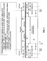
- Figure 1 is a cross-section of a ridge waveguide device in accordance with the present invention in which pedestals are located on the carrier wafer along dicing streets, prior to dicing from the assembled wafer structure;
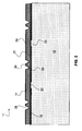
- Figure 2 is an enlarged cross-section of a portion of a further embodiment of the present invention in which pedestals are distributed across the waveguide device;
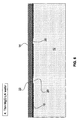
- Figure 3 illustrates a first step in a method in accordance with the present invention in which trenches are etched in a carrier wafer to form pedestals;
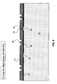
- Figure 4 illustrates a further step to the method from Figure 3, in which an SiO 2 cladding is applied to a MgO doped LN transmissive wafer prior to joining the two wafers;
- Figure 5 illustrates a further step to the method from Figure 4, in which adhesive is introduced to the space between the wafers by wicking;
- Figure 6 illustrates a further step to the method from Figure 5, in which the MgO doped LN transmissive wafer is thinned;
- Figure 7 illustrates a further step to the method from Figure 6, in which trenches are etched into the thinned MgO doped LN wafer to form ridge waveguides;
- Figure 8 illustrates a further step to the method from Figure 7, in which a cladding coating of SiO 2 is deposited over the etched MgO doped LN wafer;
- Figure 9 is a cross-section of another embodiment of the ridge waveguide device in accordance with the present invention, in which the ridge waveguides are formed on the joining surface of the transmissive wafer with pedestals in the carrier wafer aligned on the dicing streets, prior to dicing from the assembled wafer structure;
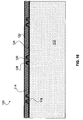
- Figure 10 is cross-section of a portion of the waveguide device of Figure 9;
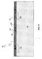
- Figure 11 is a further embodiment of the waveguide device of the present invention, in which pedestals of SiO 2 on the joining surface of the transmissive wafer surround each ridge waveguide of the device;
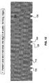
- Figure 12 illustrates a first step in a alternative method in accordance with the present invention in which trenches are etched in the joining surface of a MgO doped LN transmissive wafer to form ridge waveguides;
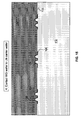
- Figure 13 illustrates a further step to the method from Figure 12, in which an SiO 2 cladding layer is deposited over the joining surface of the transmissive wafer;
- Figure 14 illustrates a further step to the method from Figure 13, in which the SiO 2 cladding layer is etched back without removing the cladding from the ridge waveguide areas;
- Figure 15 illustrates a further step to the method from Figure 14, in which the joining surface of the transmissive wafer is joined to a joining surface of the carrier wafer showing the interstices formed by the pedestals of remaining SiO 2 cladding;
- Figure 16 illustrates a further step to the method from Figure 15, in which adhesive is introduced into the interstices by wicking;
- Figure 17 illustrates a further step to the method from Figure 16, in which the MgO doped LN transmissive wafer is thinned on its exterior surface;
- Figure 18 illustrates a further step to the method from Figure 17, in which a cladding layer of SiO 2 is deposited on the exterior surface of the transmissive wafer;
- Figure 19 is a cross-section of an assembled wafer structure including a carrier wafer and a transmissive wafer with pedestals surrounded by adhesive between them.
- Second harmonic generation is a commonly practiced technique for obtaining coherent light at short wavelengths from long wavelength laser sources. It is a non-linear process where an optical beam, called the pump beam, interacts with an optically non-linear medium, in the case of second harmonic generation, to generate a second harmonic beam, where the frequency of the second harmonic beam is twice the frequency of the pump beam. Equivalently, the free space wavelength of the second harmonic is half the free space wavelength of the pump. Any material which lacks inversion symmetry can be used as the optically non-linear medium for second harmonic generation. Materials which are commonly used include lithium niobate, MgO-doped lithium niobate and KTP (KTiOPO 4 ). Second-harmonic generation is one of a class of methods, known collectively as non-linear frequency mixing, which employ similar ridge waveguide optical structures to generate or amplify coherent light at a desired wavelength from light at an input, or from a pump.
- FIG. 1 is a cross section illustrating a completed ridge waveguide assembly 10 (prior to dicing from the wafer) manufactured in accordance with the present invention.
- multiple ridge waveguides 30, in this case 11 are formed on a single chip.
- Each waveguide 30 has a slightly different conversion wavelength, which increases the probability that a ridge waveguide 30 with the correct conversion wavelength lies within the device.
- the waveguides are designed to operate at a specified laser input and output wavelength.
- the acceptance bandwidth of the waveguide is narrow, and small deviations of the waveguide dimensions can shift the operating center wavelength (CWL) too far from the specified laser input wavelength. Dimensional variation due to processing can be compensated by forming several adjacent waveguides on one device.
- Each ridge waveguide 30 within the device 10 may have slightly different lateral dimensions, or include a periodically-poled region of slightly different period.
- the conversion wavelength of each ridge waveguide 30 is measured, and the suitable waveguides are identified.
- the use of multiple, slightly different, ridge waveguides 30 improves the manufacturing yield.
- the ridge waveguide device 10 comprises a carrier wafer 12 and a transmissive layer 14 of optically non-linear material each having a joining surface secured by an adhesive layer 16.
- the transmissive layer 14, as mentioned above is an optically non-linear material such as lithium niobate, MgO doped lithium niobate, or KTP.
- the carrier wafer 12 is preferably a material having a coefficient of thermal expansion (CTE) very close to that of the transmissive layer 14, in all directions.
- the carrier wafer 12 is polished to a surface parallelism within 0.005 microns.
- a preferred assembly includes a lithium niobate carrier wafer 12 and MgO doped lithium niobate transmissive layer 14.
- the carrier wafer 12 is etched with wide trenches 18 (see Fig. 3) leaving pedestals 20 along the dicing streets.
- the tops of the pedestals 20 retain the reference plane of the polished carrier wafer 12.
- Pedestals 20 can be narrow such that they will be removed by the dicing saw; alternatively, they can be wide enough that pedestals remain in the diced devices.
- the trench depth is approximately 1 micron.
- the pedestal height of 1 micron controls the adhesive layer 16 in the trench 18 to this thickness, while the transmissive wafer 14 is supported by the tops of the pedestals 20 on the reference plane of the carrier wafer 12.
- the transmissive wafer 14 is supported by the tops of the pedestals 20 on the reference plane of the carrier wafer 12.
- the adhesive layer 16 is interrupted by a plurality of pedestals 20 within the device, which are not removed by dicing.
- the pedestals 20 are constructed of a hard, dense material which forms a solid relief structure in direct contact with the wafers 12,14. Adhesive is introduced into the interstices between the wafers 12,14 and surrounding the pedestals 20.
- Pedestals 20 can be formed by etching trenches 18 from the surface of the carrier wafer 12 through a photomask. Alternatively, pedestals 20 can be formed by depositing a highly uniform, thin layer onto the joining surface 13 of the carrier wafer 12, or the joining surface 15 of the transmissive wafer 14.
- This deposited layer is etched back to create a relief pattern of pedestals 20 into which adhesive can be introduced, by wicking or pressing for example.
- the deposited layer is applied through a shadow mask or a photolithography mask to create a relief pattern of pedestals 20.
- the pedestals 20 can be formed by deposition over a patterned photo resist and subsequent lift-off.
- the pedestals 20 are formed of a deposited layer which is of a material selected to be differentially etchable to the carrier wafer.
- a deposited layer which is of a material selected to be differentially etchable to the carrier wafer.
- an SiO 2 or Ta 2 O 5 layer is easily chemically etched and lithium niobate acts as an etch stop.
- the deposited layer is selected from a material optically similar to the adhesive, as this simplifies the thickness metrology.
- Most oxide dielectrics are suitable, as are durable metals such as Cr, Ni and Ti/W.
- a precise uniform layer can be applied by physical vapor deposition (PVD) including,sputtering, electron beam, ion assisted, or atomic layer deposition, for example.
- Chemical vapor deposition (CVD) techniques are also sufficient, such as plasma enhanced CVD.
- deposited pedestals 20 must have a height uniformity of 0.05 microns and preferably within 0.01 microns.
- the relief pattern preferably creates continuous channels open at either end to facilitate adhesive wicking.
- adhesive may be introduced on one or both joining surfaces 13,15 prior to assembly, subsequently pressure is applied to bring the joining surfaces into contact with the pedestals 20.
- Fig. 2 illustrates a narrow pedestal 20 between each ridge waveguide 30 on the device 11, while Fig. 1 shows wide pedestals 20 only at the periphery of the device 10, where a dicing saw will cut the assembly into individual devices.
- the wide pedestals can be designed to be completely removed by the dicing saw, or to remain in the finished device.
- a device can contain either narrow or wide pedestals or both.
- One benefit of leaving the pedestals in the periphery of the final device is to reduce the outgassing rate of the adhesive. This is of particular interest for device lifetime reasons in hermetic packages. Pedestals also contribute to a more dimensionally stable structure that resists slumping which might disrupt waveguide alignment over time.
- the optical properties of the joining layer do not affect the optical function of the waveguide device.
- the adhesive may be amorphous or crystalline, may be transparent, scattering or opaque and may have any refractive index and absorption coefficient.
- a preferred adhesive is low viscosity, particle-free, cures without evolving gasses, has low shrinkage, low stress, is capable of withstanding subsequent processing steps and is permanent.
- An example of a preferred adhesive includes UV 15LV, from MasterBond
- the wafer scale process according to the present invention can produce approximately 200 devices depending on the waveguide design, over a 3 inch wafer, in the same production time and energy consumption as current processes expend on a single device. Furthermore, the devices manufactured according to the wafer scale process of the present invention have a number of advantages over the prior art as discussed above.
- Figs. 3-8 illustrate a first method in accordance with the present invention.
- a lithium niobate carrier wafer 12 is polished to have a surface parallelism within 0.005 microns, and preferably within 0.001 microns.
- the carrier wafer 12 is patterned and etched to form broad shallow trenches 18 in the joining surface 13 leaving pedestals 20 between them.
- the trenches 18 are between 0.5 microns and 5 microns deep, preferably 1.0 microns deep.
- the carrier wafer 12 is preferably congruent lithium niobate of the same crystal orientation as the MgO-doped lithium niobate waveguide layer, a material of lower cost than the waveguide layer, and readily available in all size wafers.
- the pedestals 20 can be located between each ridge waveguide 30 or located only at the perimeter of each device 10, as shown in Fig 1. Adding pedestals 20 between ridge waveguides 30 improves the control of the waveguide layer reference to the carrier wafer surface. However, increasing the number of pedestals 20 does reduce the surface area of adhesive, reducing the strength of the adhesive bond. Thus, the relief pattern of pedestals must balance these factors.
- the level of accuracy of the present invention is controlled across wafers of up to 3 inch diameter, and can be applied to larger wafers.
- the surfaces need to be clean and particle-free. External uniform pressure is preferably applied
- the bottom SiO 2 coating 22 can be eliminated if the pedestals 20 are not underneath a ridge waveguide 30, though the SiO 2 coating may improve adhesion of the assembly.
- adhesive 16 is wicked into the gap created by the pedestals 20.
- the use of a cladding layer 22 eliminates any optical property specification for the adhesive material.
- the MgO-doped lithium niobate material 14 is thinned, preferably by optical lap grinding and polishing, but could be thinned by etching such as Reactive-Ion-Etching (RIE).
- etching such as Reactive-Ion-Etching (RIE).
- trenches 28 are formed into the thinned lithium niobate layer 14, as shown in Fig. 7.
- trenches may be formed via Reactive Ion Etching (RIE) or with laser milling.
- the layer of lithium niobate remaining underneath these etched trenches 28 is called the planar slab region 26.
- the thinned and etched lithium niobate layer 14 can have a coating 24 applied, as shown in Fig. 8.
- the top coating 24 is optional.
- the top coating 24 acts as a cladding, as well as, reducing the effect of contaminants on the operational charactgeristics of the device 10.
- the coating 24 may also include some conductivity, to dissipate pyroelectric generated charge.
- Reactive Ion Etching in an inductively coupled plasma is a preferred method for etching trenches 28. It comprises a method to chemically impose a topographical change in the surface of the waveguide layer 14.
- the waveguide 30 is formed by removing material on both sides of a narrow ridge.
- the ridge becomes a waveguide 30.
- ICP-RIE is not a mechanical working process.
- Figs. 9 - 11 show preferred embodiments of the frequency doubling device 100, where the ridge waveguides 130 are upside down.
- the planar slab region 126 is above the ridge 130, instead of underneath it.
- the carrier wafer 112 is still beneath the ridge 130, as it was in Figs. 1 - 8.
- the adhesive layer116 is continuous underneath all the ridges 130.
- the carrier wafer 112 is etched to create wide trenches 118 separated by pedestals 120. As shown in Fig. 9, these are centered on the dicing streets. Thus the pedestals 120 do not show in the diced chip shown in Fig. 10.
- Fig. 9 show preferred embodiments of the frequency doubling device 100, where the ridge waveguides 130 are upside down.
- the planar slab region 126 is above the ridge 130, instead of underneath it.
- the carrier wafer 112 is still beneath the ridge 130, as it was in Figs. 1 - 8.
- the adhesive layer116 is continuous underneath all the ridges 130.
- the SiO 2 cladding layer 124 is etched beyond the waveguiding area, including the ridge 130 and the slab region 126 above the trenches 128, to form a relief pattern comprising the pedestals 120 needed to control the adhesive thickness. Additional efficiency is realized in forming the pedestals 120 from the cladding layer 124.
- Figs. 12 - 18 describe the fabrication process for this second version of the upside down ridge 100.
- trenches 128 are etched into surface of an MgO-doped LN wafer 114. In this case in the joining surface 115.
- the orientation of the wafer 114 shows the trenches 128 to be on the bottom, simply to be consistent with the following figures.
- an SiO 2 coating 124 is applied over the trenches 128 and ridges 130.
- the SiO 2 coating is removed in certain regions, forming pedestals 120 needed for controlling the adhesive thickness.
- the MgO-doped lithium niobate wafer 114 is contacted with a carrier wafer 112, preferably a congruent lithium niobate wafer.
- adhesive 116 is introduced into the gap created by the patterned SiO 2 coating pedestals 120 and the trenches 128 that form the ridges 130.
- the MgO-doped lithium niobate material 114 is thinned by polishing or etching.
- An optional top coating 122 of SiO 2 is applied in Fig. 18. As before, the top coating 122 acts as a cladding, protects the surface of the thinned LN layer from contamination, and may also include some conductivity, to dissipate pyroelectric generated charge.
- Tolerances in the method of the present invention to achieve wafer scale yield across a 4" wafer must result in finished devices having a thickness variation in the waveguide layer of within 0.5 microns, and preferably within 0.1 microns.
- the carrier wafer must have a surface parallelism equal to the finished tolerance of 0.5 microns or better, and a deposited pedestal height must have a uniformity within 0.05 microns and preferably within 0.01 microns.
- waveguide reliability and fabrication yield are improved by means of a substrate that is electrically conducting.
- a substrate that is electrically conducting.
- ferroelectric material for the waveguide such as lithium niobate
- CTE matching minimizes or eliminates thermally induced strain in the waveguide, thereby improving its wavelength stability and long term reliability.
- endfaces of the individual ridge waveguide devices are polished to laser quality level.
- Anti-reflective coatings for the input and output wavelengths may be applied as required to enhance coupling efficiency
- the wafer scale process illustrated generally by the wafer assembly shown in Figure 19, is a method of adhesively securing a wafer of optically transmissive material 14 to a carrier wafer 12 having a parallelism within 0.5 microns, more preferably within 0.1 microns and accurately transferring that surface information to the joining surface 15 of the transmissive wafer 14.
- a very thin optical waveguiding layer can be created with a thickness variation of within 0.1 micron. This is accomplished by creating a relief pattern by etching into the joining surface 13 of the carrier wafer 12 to create a space 18 into which to introduce adhesive while placing the transmissive wafer 14 in direct contact with the reference surface 13 of the carrier wafer 12.
- the relief pattern is created by depositing a uniform layer over the joining surface 13, 15 of the carrier wafer 12 or the transmissive wafer 14 through a shadow mask or photolithographic mask; or by depositing a uniform layer over a patterned photo resist and subsequent lift-off.
- the pedestals 20 left standing in the relief pattern have a uniform height, within 0.1 microns, which transfer the surface information from the carrier wafer 12 to the joining surface 15 of the transmissive wafer 14.
- This method can be used in wafer scale production of planar lightwave circuits (PLC) with highly uniform dimensions.
- PLC planar lightwave circuits
- this method can be used in wafer scale manufacture of electro-optic waveguide devices with very thin indiffused waveguides to reduce voltage requirements.
Landscapes
- Physics & Mathematics (AREA)
- General Physics & Mathematics (AREA)
- Optics & Photonics (AREA)
- Nonlinear Science (AREA)
- Engineering & Computer Science (AREA)
- Microelectronics & Electronic Packaging (AREA)
- Optical Integrated Circuits (AREA)
- Optical Modulation, Optical Deflection, Nonlinear Optics, Optical Demodulation, Optical Logic Elements (AREA)
Abstract
Description
- The present invention relates to a wafer scale process for the manufacture of optical waveguide devices, and particularly for the manufacture of ridge waveguide devices, and the improved ridge waveguides made thereby.
- Optical waveguide devices require a high degree of accuracy in the dimensions of the optical waveguiding layer. In the past it has not been possible to achieve the degree of parallelism and uniformity in a wafer scale manufacturing process that would enable an adequate yield across the wafer, and from wafer to wafer. A wafer of optically transmissive material thinned and polished to waveguide dimensions of approximately 1-10 microns does not have the dimensional stability to be polished to or to hold the flatness required, or even to be handled without breaking. In order to achieve the degree of parallelism required in a thin optical material, a master reference plane must be provided in a carrier substrate wafer. It is known in the art to polish wafers to a uniformity of parallelism within 0.005 microns. However, for wafer scale manufacture, this precision is not transferred to the thin waveguiding layer due to variation introduced by the adhesive layer securing the waveguiding layer to the carrier substrate. Optical devices such as planar lightwave circuits, electro-optic modulators and ridge waveguide devices are examples of optical waveguide devices for which dimensional uniformity is essential to achieve wafer scale production.
- Second harmonic generation applications (frequency doubling) using ridge waveguide devices have been developed to create laser output in the ultraviolet, visible and infrared wavelength spectrum for use in numerous technologies. Demand for these devices is high. However, the manufacture of ridge waveguide devices has been limited to individual device processing. One problem that arises in the manufacture of ridge waveguides for the application of second harmonic generation is the control of dimensions of the ridge. In particular the thicknesses of the ridge waveguide must be controlled accurately, due to sensitivity of the upconversion wavelength to all dimensions of the ridge. Lateral dimensions are controlled with photolithographic processes, while vertical dimensions are controlled by etching and polishing processes.
- Ridge waveguide devices for second harmonic generation considered in this application have periodically poled regions in the waveguides for phase matching the pump and output signals. Adhesive assembly of the supporting carrier wafer and optically transmissive wafer is preferred. In order to achieve adequate manufacturing yield, the range of thickness of the ridge and planar slab region must be controlled to within a few tenths of a micron. In order to achieve this level of uniformity across the wafer and from wafer-to-wafer, the thickness of the adhesive between the transmissive wafer and carrier wafer must be controlled to within this same range. This level of control for wafer scale manufacture has not been demonstrated in the prior art.
- An optical wavelength conversion element is disclosed in
US patent No. 6,631,231 by Kiminori Mizuuchi et al. issued to Matsushita Electric Industrial Co. Ltd. on October 7, 2003. In this patent a continuous joining layer of amorphous material is used to join a poled waveguide structure to a substrate layer. No method for controlling the adhesive thickness is disclosed, although the disclosure does recognize some critical optical limitations to adhesive thickness. Instead, significant post assembly finishing is disclosed. These are labor intensive methods for individual device production. Such methods do not produce high yield. Furthermore, the Mizuuchi design is dependent on the optical properties of the adhesive layer, which limits the design choice. - Adhesive layer spacing is known in various optical industries. For instance glass fiber particles are disclosed for use as spacers between LCD display screen layers in
US patent No. 4,390,245 .US patent No. 6,896,949 disclosing the wafer scale manufacture of etalons also makes use of small beads to facilitate spacing between plural assembled etalons, or of fritted glass which is applied to a certain thickness and heated to its melting point to join etalon elements. An image sensor as disclosed inUS patent No. 5,433,911 also discloses the assembly of an individual device, using spacers constructed through resist patterning in order to secure a protective cover with controlled parallelism. However, none of these disclosures provide instruction for adhesive assembly suitable for the present application that can provide the level of accuracy necessary for wafer scale production control across the wafer and from wafer to wafer. Beads and spacers available in the industry do not provide the uniformity within 0.1 microns deviation needed to ensure tolerance control across the wafer. - A wafer scale manufacturing process for optical waveguide devices, and ridge waveguide devices in particular, remains highly desired in the industry.
- An object of the present invention is to provide a wafer scale manufacturing process for producing optical waveguide devices with sub micron accuracy and high yield.
- It is a further objective of the present invention to provide a ridge waveguide device made in accordance with the manufacturing process of the present invention including rigid spacing elements within a precisely dimensioned discontinuous adhesive layer.
- The present invention has found a process for achieving sub-micron control of an optical waveguiding layer thickness by providing a dimensionally stable wafer assembly into which adhesive can be introduced without altering the planar relationship between a carrier wafer and an optically transmissive wafer in wafer scale manufacture. This process permits the required dimensional control of ridge and slab in ridge waveguide devices in wafer scale manufacture. More generally, this process permits wafer scale manufacture of optical waveguide devices including thin optically transmissive layers. In particular, a pattern of spacer pedestals is created by a deposition and etch back, or by a surface etch process to precisely reference the joining surface of the optically transmissive wafer to the joining surface of the carrier wafer which is by necessity parallel to the exposed surface of the carrier wafer which is in turn referenced to a reusable master surface. The tolerance achievable in accordance with this process provides consistent yield across the wafer. The process additionally provides enhanced structural integrity to the finished devices.
- Accordingly, the present invention relates to a wafer scale process for manufacturing optical waveguide devices comprising the steps of:
- providing a transmissive wafer of optically transmissive material having a joining surface and an exterior surface;
- providing a carrier wafer having a joining surface and an exterior surface substantially parallel to the joining surface;
- creating a relief pattern on one of the joining surfaces, the relief pattern comprising pedestals having a substantially uniform height;
- contacting the pedestals with the joining surface of the other wafer and
- introducing adhesive material into the spaces created by the relief pattern;
- polishing and thinning the transmissive wafer to a prescribed dimension;
- creating a waveguide structure in the transmissive wafer;
- dicing the assembled wafer structure into individual waveguide devices.
- The present invention further relates to a wafer scale process wherein the waveguide structure is selected from the group consisting of : ridge waveguide, indiffused waveguide, and planar waveguide.
- Another aspect of the present invention relates to a method of manufacturing optical ridge waveguide devices comprising the steps of:
- providing a transmissive wafer of optically non-linear transmissive material having a joining surface and an exterior surface;
- providing a carrier wafer having a joining surface and an exterior surface;
- applying a cladding layer to the joining surface of the optically transmissive wafer including the waveguide structure,;
- etching a portion of the cladding layer to the joining surface, without removing the cladding on the waveguide structure, to create a relief pattern adapted to facilitate an adhesive joint between the joining surfaces;
- contacting the cladding layer to the joining surface of the carrier wafer, and introducing adhesive into the spaces created by the relief pattern;
- polishing and thinning the exterior surface of the transmissive wafer;
- creating a waveguide structure in the joining surface of the optically transmissive wafer; dicing the assembled wafer structure into individual waveguide devices.
- Another feature of the present invention provides an optical waveguide device comprising:
- a carrier substrate having a joining surface substantially parallel to an exterior surface;
- an optically transmissive substrate adhesively joined to the carrier substrate having a waveguide formed therein;
- a plurality of rigid pedestals abutting a joining surface of the carrier substrate and a joining surface of the transmissive substrate; and
- a discontinuous adhesive layer surrounding the pedestals and securing the joining surface of the carrier substrate to the joining surface of the transmissive substrate, having a uniform thickness defined by a height of the pedestals.
- The invention will be described in greater detail with reference to the accompanying drawings which represent preferred embodiments thereof, wherein:
- Figure 1 is a cross-section of a ridge waveguide device in accordance with the present invention in which pedestals are located on the carrier wafer along dicing streets, prior to dicing from the assembled wafer structure;
- Figure 2 is an enlarged cross-section of a portion of a further embodiment of the present invention in which pedestals are distributed across the waveguide device;
- Figure 3 illustrates a first step in a method in accordance with the present invention in which trenches are etched in a carrier wafer to form pedestals;
- Figure 4 illustrates a further step to the method from Figure 3, in which an SiO2 cladding is applied to a MgO doped LN transmissive wafer prior to joining the two wafers;
- Figure 5 illustrates a further step to the method from Figure 4, in which adhesive is introduced to the space between the wafers by wicking;
- Figure 6 illustrates a further step to the method from Figure 5, in which the MgO doped LN transmissive wafer is thinned;
- Figure 7 illustrates a further step to the method from Figure 6, in which trenches are etched into the thinned MgO doped LN wafer to form ridge waveguides;
- Figure 8 illustrates a further step to the method from Figure 7, in which a cladding coating of SiO2 is deposited over the etched MgO doped LN wafer;
- Figure 9 is a cross-section of another embodiment of the ridge waveguide device in accordance with the present invention, in which the ridge waveguides are formed on the joining surface of the transmissive wafer with pedestals in the carrier wafer aligned on the dicing streets, prior to dicing from the assembled wafer structure;
- Figure 10 is cross-section of a portion of the waveguide device of Figure 9;
- Figure 11 is a further embodiment of the waveguide device of the present invention, in which pedestals of SiO2 on the joining surface of the transmissive wafer surround each ridge waveguide of the device;
- Figure 12 illustrates a first step in a alternative method in accordance with the present invention in which trenches are etched in the joining surface of a MgO doped LN transmissive wafer to form ridge waveguides;
- Figure 13 illustrates a further step to the method from Figure 12, in which an SiO2 cladding layer is deposited over the joining surface of the transmissive wafer;
- Figure 14 illustrates a further step to the method from Figure 13, in which the SiO2 cladding layer is etched back without removing the cladding from the ridge waveguide areas;
- Figure 15 illustrates a further step to the method from Figure 14, in which the joining surface of the transmissive wafer is joined to a joining surface of the carrier wafer showing the interstices formed by the pedestals of remaining SiO2 cladding;
- Figure 16 illustrates a further step to the method from Figure 15, in which adhesive is introduced into the interstices by wicking;
- Figure 17 illustrates a further step to the method from Figure 16, in which the MgO doped LN transmissive wafer is thinned on its exterior surface;
- Figure 18 illustrates a further step to the method from Figure 17, in which a cladding layer of SiO2 is deposited on the exterior surface of the transmissive wafer;
- Figure 19 is a cross-section of an assembled wafer structure including a carrier wafer and a transmissive wafer with pedestals surrounded by adhesive between them.
- Second harmonic generation is a commonly practiced technique for obtaining coherent light at short wavelengths from long wavelength laser sources. It is a non-linear process where an optical beam, called the pump beam, interacts with an optically non-linear medium, in the case of second harmonic generation, to generate a second harmonic beam, where the frequency of the second harmonic beam is twice the frequency of the pump beam. Equivalently, the free space wavelength of the second harmonic is half the free space wavelength of the pump. Any material which lacks inversion symmetry can be used as the optically non-linear medium for second harmonic generation. Materials which are commonly used include lithium niobate, MgO-doped lithium niobate and KTP (KTiOPO4). Second-harmonic generation is one of a class of methods, known collectively as non-linear frequency mixing, which employ similar ridge waveguide optical structures to generate or amplify coherent light at a desired wavelength from light at an input, or from a pump.
- Figure 1 is a cross section illustrating a completed ridge waveguide assembly 10 (prior to dicing from the wafer) manufactured in accordance with the present invention. In this embodiment
multiple ridge waveguides 30, in thiscase 11, are formed on a single chip. Eachwaveguide 30 has a slightly different conversion wavelength, which increases the probability that aridge waveguide 30 with the correct conversion wavelength lies within the device. The waveguides are designed to operate at a specified laser input and output wavelength. The acceptance bandwidth of the waveguide is narrow, and small deviations of the waveguide dimensions can shift the operating center wavelength (CWL) too far from the specified laser input wavelength. Dimensional variation due to processing can be compensated by forming several adjacent waveguides on one device. Eachridge waveguide 30 within thedevice 10 may have slightly different lateral dimensions, or include a periodically-poled region of slightly different period. The conversion wavelength of eachridge waveguide 30 is measured, and the suitable waveguides are identified. Hence, the use of multiple, slightly different,ridge waveguides 30 improves the manufacturing yield. - As shown in Fig. 1, the
ridge waveguide device 10 comprises acarrier wafer 12 and atransmissive layer 14 of optically non-linear material each having a joining surface secured by anadhesive layer 16. Thetransmissive layer 14, as mentioned above is an optically non-linear material such as lithium niobate, MgO doped lithium niobate, or KTP. Thecarrier wafer 12 is preferably a material having a coefficient of thermal expansion (CTE) very close to that of thetransmissive layer 14, in all directions. Thecarrier wafer 12 is polished to a surface parallelism within 0.005 microns. A preferred assembly includes a lithiumniobate carrier wafer 12 and MgO doped lithiumniobate transmissive layer 14. Thecarrier wafer 12 is etched with wide trenches 18 (see Fig. 3) leavingpedestals 20 along the dicing streets. The tops of thepedestals 20 retain the reference plane of thepolished carrier wafer 12.Pedestals 20 can be narrow such that they will be removed by the dicing saw; alternatively, they can be wide enough that pedestals remain in the diced devices. The trench depth is approximately 1 micron. Thus the pedestal height of 1 micron controls theadhesive layer 16 in thetrench 18 to this thickness, while thetransmissive wafer 14 is supported by the tops of thepedestals 20 on the reference plane of thecarrier wafer 12. Alternatively, as can be seen more clearly in the enlarged section of theembodiment 11 illustrated in Fig. 2, theadhesive layer 16 is interrupted by a plurality ofpedestals 20 within the device, which are not removed by dicing. Thepedestals 20 are constructed of a hard, dense material which forms a solid relief structure in direct contact with thewafers wafers pedestals 20.Pedestals 20 can be formed by etchingtrenches 18 from the surface of thecarrier wafer 12 through a photomask. Alternatively, pedestals 20 can be formed by depositing a highly uniform, thin layer onto the joiningsurface 13 of thecarrier wafer 12, or the joiningsurface 15 of thetransmissive wafer 14. This deposited layer is etched back to create a relief pattern ofpedestals 20 into which adhesive can be introduced, by wicking or pressing for example. The deposited layer is applied through a shadow mask or a photolithography mask to create a relief pattern ofpedestals 20. Alternatively thepedestals 20 can be formed by deposition over a patterned photo resist and subsequent lift-off. - Preferably the
pedestals 20 are formed of a deposited layer which is of a material selected to be differentially etchable to the carrier wafer. For example, an SiO2 or Ta2O5 layer is easily chemically etched and lithium niobate acts as an etch stop. In addition, it is advantageous if the deposited layer is selected from a material optically similar to the adhesive, as this simplifies the thickness metrology. Most oxide dielectrics are suitable, as are durable metals such as Cr, Ni and Ti/W. A precise uniform layer can be applied by physical vapor deposition (PVD) including,sputtering, electron beam, ion assisted, or atomic layer deposition, for example. Chemical vapor deposition (CVD) techniques are also sufficient, such as plasma enhanced CVD. For manufacturing tolerances, depositedpedestals 20 must have a height uniformity of 0.05 microns and preferably within 0.01 microns. - The relief pattern preferably creates continuous channels open at either end to facilitate adhesive wicking. Alternatively adhesive may be introduced on one or both joining
surfaces pedestals 20. Fig. 2 illustrates anarrow pedestal 20 between eachridge waveguide 30 on thedevice 11, while Fig. 1 showswide pedestals 20 only at the periphery of thedevice 10, where a dicing saw will cut the assembly into individual devices. The wide pedestals can be designed to be completely removed by the dicing saw, or to remain in the finished device. Furthermore, a device can contain either narrow or wide pedestals or both. One benefit of leaving the pedestals in the periphery of the final device is to reduce the outgassing rate of the adhesive. This is of particular interest for device lifetime reasons in hermetic packages. Pedestals also contribute to a more dimensionally stable structure that resists slumping which might disrupt waveguide alignment over time. - The optical properties of the joining layer do not affect the optical function of the waveguide device. The adhesive may be amorphous or crystalline, may be transparent, scattering or opaque and may have any refractive index and absorption coefficient. A preferred adhesive is low viscosity, particle-free, cures without evolving gasses, has low shrinkage, low stress, is capable of withstanding subsequent processing steps and is permanent. An example of a preferred adhesive includes UV 15LV, from MasterBond
- The wafer scale process according to the present invention can produce approximately 200 devices depending on the waveguide design, over a 3 inch wafer, in the same production time and energy consumption as current processes expend on a single device. Furthermore, the devices manufactured according to the wafer scale process of the present invention have a number of advantages over the prior art as discussed above.
- Figs. 3-8 illustrate a first method in accordance with the present invention. In accordance with the first method as shown in Fig. 3, a lithium
niobate carrier wafer 12 is polished to have a surface parallelism within 0.005 microns, and preferably within 0.001 microns. Thecarrier wafer 12 is patterned and etched to form broadshallow trenches 18 in the joiningsurface 13 leavingpedestals 20 between them. Thetrenches 18 are between 0.5 microns and 5 microns deep, preferably 1.0 microns deep. Thecarrier wafer 12 is preferably congruent lithium niobate of the same crystal orientation as the MgO-doped lithium niobate waveguide layer, a material of lower cost than the waveguide layer, and readily available in all size wafers. Thepedestals 20 can be located between eachridge waveguide 30 or located only at the perimeter of eachdevice 10, as shown in Fig 1. Adding pedestals 20 betweenridge waveguides 30 improves the control of the waveguide layer reference to the carrier wafer surface. However, increasing the number ofpedestals 20 does reduce the surface area of adhesive, reducing the strength of the adhesive bond. Thus, the relief pattern of pedestals must balance these factors. The level of accuracy of the present invention is controlled across wafers of up to 3 inch diameter, and can be applied to larger wafers. - In Fig. 4, a thick Mg-doped
lithium niobate wafer 14, surface coated with anappropriate cladding material 22, such as SiO2 on the joiningsurface 15, is contacted to the joiningsurface 13 of thecarrier wafer 12. The surfaces need to be clean and particle-free. External uniform pressure is preferably applied The bottom SiO2 coating 22 can be eliminated if thepedestals 20 are not underneath aridge waveguide 30, though the SiO2 coating may improve adhesion of the assembly. In Fig. 5, adhesive 16 is wicked into the gap created by thepedestals 20. The use of acladding layer 22 eliminates any optical property specification for the adhesive material. - In Fig. 6, the MgO-doped
lithium niobate material 14 is thinned, preferably by optical lap grinding and polishing, but could be thinned by etching such as Reactive-Ion-Etching (RIE). After thinning,trenches 28 are formed into the thinnedlithium niobate layer 14, as shown in Fig. 7. For exampled trenches may be formed via Reactive Ion Etching (RIE) or with laser milling. The layer of lithium niobate remaining underneath these etchedtrenches 28 is called theplanar slab region 26. The thinned and etchedlithium niobate layer 14 can have acoating 24 applied, as shown in Fig. 8. Thetop coating 24 is optional. It protects the surface of the thinnedlithium niobate layer 14 from contamination. Thetop coating 24 acts as a cladding, as well as, reducing the effect of contaminants on the operational charactgeristics of thedevice 10. Thecoating 24 may also include some conductivity, to dissipate pyroelectric generated charge. - Reactive Ion Etching in an inductively coupled plasma (ICP-RIE) is a preferred method for etching
trenches 28. It comprises a method to chemically impose a topographical change in the surface of thewaveguide layer 14. When the topography consists of trenches narrowly spaced, thewaveguide 30 is formed by removing material on both sides of a narrow ridge. When the ridge is formed to the requisite width and height above thelower cladding layer 22, the ridge becomes awaveguide 30. ICP-RIE is not a mechanical working process. - Figs. 9 - 11 show preferred embodiments of the
frequency doubling device 100, where theridge waveguides 130 are upside down. Theplanar slab region 126 is above theridge 130, instead of underneath it. Thecarrier wafer 112 is still beneath theridge 130, as it was in Figs. 1 - 8. In Figs. 9 and 10, the adhesive layer116 is continuous underneath all theridges 130. As in Fig. 1, thecarrier wafer 112 is etched to create wide trenches 118 separated bypedestals 120. As shown in Fig. 9, these are centered on the dicing streets. Thus thepedestals 120 do not show in the diced chip shown in Fig. 10. Fig. 11 shows a second version of the upside down ridge, where the adhesive layer is not continuous across the width of the device. For this embodiment, the SiO2 cladding layer 124 is etched beyond the waveguiding area, including theridge 130 and theslab region 126 above thetrenches 128, to form a relief pattern comprising thepedestals 120 needed to control the adhesive thickness. Additional efficiency is realized in forming thepedestals 120 from thecladding layer 124. - Figs. 12 - 18 describe the fabrication process for this second version of the upside down
ridge 100. In Fig. 12,trenches 128 are etched into surface of an MgO-dopedLN wafer 114. In this case in the joiningsurface 115. The orientation of thewafer 114 shows thetrenches 128 to be on the bottom, simply to be consistent with the following figures. In Fig. 13, an SiO2 coating 124 is applied over thetrenches 128 andridges 130. In Fig. 14, the SiO2 coating is removed in certain regions, formingpedestals 120 needed for controlling the adhesive thickness. - In Fig. 15, the MgO-doped
lithium niobate wafer 114 is contacted with acarrier wafer 112, preferably a congruent lithium niobate wafer. In Fig. 16, adhesive 116 is introduced into the gap created by the patterned SiO2 coating pedestals 120 and thetrenches 128 that form theridges 130. In Fig. 17, the MgO-dopedlithium niobate material 114 is thinned by polishing or etching. An optionaltop coating 122 of SiO2 is applied in Fig. 18. As before, thetop coating 122 acts as a cladding, protects the surface of the thinned LN layer from contamination, and may also include some conductivity, to dissipate pyroelectric generated charge. - Tolerances in the method of the present invention to achieve wafer scale yield across a 4" wafer must result in finished devices having a thickness variation in the waveguide layer of within 0.5 microns, and preferably within 0.1 microns. To obtain this, the carrier wafer must have a surface parallelism equal to the finished tolerance of 0.5 microns or better, and a deposited pedestal height must have a uniformity within 0.05 microns and preferably within 0.01 microns.
- In this preferred embodiment, waveguide reliability and fabrication yield are improved by means of a substrate that is electrically conducting. Previous descriptions of the waveguide device use ferroelectric material for the waveguide (such as lithium niobate) and essentially the same material for the substrate, in order to optimally match the CTE of waveguide forming layer and substrate. CTE matching minimizes or eliminates thermally induced strain in the waveguide, thereby improving its wavelength stability and long term reliability.
- Once the completed wafer assembly is diced, endfaces of the individual ridge waveguide devices are polished to laser quality level. Anti-reflective coatings for the input and output wavelengths may be applied as required to enhance coupling efficiency
- The wafer scale process, illustrated generally by the wafer assembly shown in Figure 19, is a method of adhesively securing a wafer of optically
transmissive material 14 to acarrier wafer 12 having a parallelism within 0.5 microns, more preferably within 0.1 microns and accurately transferring that surface information to the joiningsurface 15 of thetransmissive wafer 14. Thus a very thin optical waveguiding layer can be created with a thickness variation of within 0.1 micron. This is accomplished by creating a relief pattern by etching into the joiningsurface 13 of thecarrier wafer 12 to create aspace 18 into which to introduce adhesive while placing thetransmissive wafer 14 in direct contact with thereference surface 13 of thecarrier wafer 12. Alternatively, the relief pattern is created by depositing a uniform layer over the joiningsurface carrier wafer 12 or thetransmissive wafer 14 through a shadow mask or photolithographic mask; or by depositing a uniform layer over a patterned photo resist and subsequent lift-off. Thepedestals 20 left standing in the relief pattern have a uniform height, within 0.1 microns, which transfer the surface information from thecarrier wafer 12 to the joiningsurface 15 of thetransmissive wafer 14. - This method can be used in wafer scale production of planar lightwave circuits (PLC) with highly uniform dimensions. Alternatively, this method can be used in wafer scale manufacture of electro-optic waveguide devices with very thin indiffused waveguides to reduce voltage requirements.
- The embodiments of the invention described above are intended to be exemplary only. The scope of the invention is therefore intended to be limited solely by the scope of the appended claims.
Claims (32)
- A wafer scale process for manufacturing optical waveguide devices comprising the steps of:providing a transmissive wafer of optically transmissive material having a joining surface and an exterior surface;providing a carrier wafer having a joining surface and an exterior surface substantially parallel to the joining surface;creating a relief pattern on one of the joining surfaces, the relief pattern comprising pedestals having a substantially uniform height;contacting the pedestals with the joining surface of the other wafer andintroducing adhesive material into the spaces created by the relief pattern;polishing and thinning the transmissive wafer to a prescribed dimension;creating a waveguide structure in the transmissive wafer;dicing the assembled wafer structure into individual waveguide devices.
- The wafer scale process in accordance with claim 1, wherein the waveguide structure is selected from the group consisting of: ridge waveguide, indiffused waveguide, and planar waveguide.
- The wafer scale process in accordance with claim 1, wherein the joining surface and the exterior surface of the carrier wafer are substantially parallel within 0.5 microns across the wafer.
- The wafer scale process in accordance with claim 3, wherein the joining surface and the exterior surface of the carrier wafer are substantially parallel within 0.1 microns across the wafer.
- The wafer scale process in accordance with claim 1 further including the step of polishing input and output end faces of the diced individual waveguide devices.
- The wafer scale process in accordance with claim 3, wherein the pedestals have a substantially uniform height within 0.05 microns across the wafer.
- The wafer scale process in accordance with claim 4, wherein the pedestals have a substantially uniform height within 0.01 microns across the wafer.
- The wafer scale process in accordance with claim 6, wherein the polished transmissive wafer has a thickness deviation of less than 0.1 micron across the wafer.
- The wafer scale process in accordance with claim 1, wherein the relief pattern is adapted to wick adhesive between the joining surfaces of the transmissive wafer and the carrier wafer.
- The wafer scale process in accordance with claim 1, wherein the step of thinning the transmissive wafer comprises thinning by reactive ion etching in an inductively coupled plasma.
- The wafer scale process in accordance with claim 2, wherein the waveguide comprises a ridge waveguide, further including the step of creating periodically poled regions on the transmissive wafer, at least in regions coinciding with the waveguide structure, prior to forming the ridge waveguide structure.
- The wafer scale process in accordance with claim 11, wherein the optical ridge waveguide devices have a thickness deviation of less than 100nm per 100mm per wafer.
- The wafer scale process in accordance with claim 11, further including the step of applying a cladding material to the joining surface of the transmissive wafer prior to contacting the pedestals with the joining surface of the other wafer.
- The wafer scale process in accordance with claim 13, further including the step of:applying a cladding material to the exterior surface of the transmissive wafer; following the step of polishing and thinning the transmissive wafer; and prior to dicing the assembled wafer structure into individual waveguide devices.
- The wafer scale process in accordance with claim 11, wherein the waveguide structure is a ridge waveguide created on the joining surface of the transmissive wafer, and the step of creating a relief pattern includes the steps of:applying a cladding layer having a uniform thickness on the joining surface of the transmissive wafer including the waveguide structure; andetching the cladding layer to create pedestals equal to the thickness of the cladding layer without removing cladding from the waveguide structure.
- The wafer scale process in accordance with claim 15, further comprising the step of:applying a cladding layer to the polished and thinned exterior surface of the transmissive wafer, prior to dicing the assembled wafer structure.
- The wafer scale process in accordance with claim 11, wherein dicing streets are defined between the waveguide devices on the assembled wafer structure, and wherein the pedestals forming the relief pattern are aligned with the dicing streets, such that the pedestals are removed from the finished waveguide devices when diced.
- The wafer scale process in accordance with claim 11, wherein dicing streets are defined between the waveguide devices on the assembled wafer structure, and wherein the pedestals forming the relief pattern are aligned with the dicing streets, the pedestals having a width such that a portion of the pedestal remains in the finished waveguide device when diced.
- The wafer scale process in accordance with claim 11, wherein dicing streets are defined between the waveguide devices on the assembled wafer structure, and wherein at least one pedestal forming the relief pattern is disposed between dicing streets and remains in the finished waveguide device when diced.
- A method of manufacturing optical waveguide devices comprising the steps of:providing a transmissive wafer of optically non-linear transmissive material having a joining surface and an exterior surface;providing a carrier wafer having a joining surface and an exterior surface;creating a ridge waveguide structure in the joining surface of the optically transmissive wafer;applying a cladding layer to the joining surface of the optically transmissive wafer including the waveguide structure,;etching a portion of the cladding layer to the joining surface, without removing the cladding on the waveguide structure, to create a relief pattern adapted to facilitate an adhesive joint between the joining surfaces;contacting the cladding layer to the joining surface of the carrier wafer, and introducing adhesive into the spaces created by the relief pattern;polishing and thinning the exterior surface of the transmissive wafer;dicing the assembled wafer structure into individual waveguide devices.
- The method of manufacturing optical waveguide devices as defined in claim 20, further including the step of forming periodically poled portions on the joining surface of the transmissive wafer at least at locations coinciding with the ridge waveguide structure.
- The method of manufacturing optical waveguide devices as defined in claim 21, wherein the ridge waveguide structure comprises a plurality of waveguide structures within each optical waveguide device, each ridge waveguide structure having a different conversion wavelength.
- An optical waveguide device comprising:a carrier substrate having a joining surface substantially parallel to an exterior surface;an optically transmissive substrate adhesively joined to the carrier substrate having a waveguide formed therein;a plurality of rigid pedestals abutting a joining surface of the carrier substrate and a joining surface of the transmissive substrate; anda discontinuous adhesive layer surrounding the pedestals and securing the joining surface of the carrier substrate to the joining surface of the transmissive substrate, having a uniform thickness defined by a height of the pedestals.
- The optical waveguide device as defined in claim 23, wherein the waveguide has a structure selected form the group consisting of: ridge waveguide, indiffused waveguide and planar waveguide.
- The optical waveguide device as defined in claim 24, wherein the waveguide comprises a ridge waveguide having periodic poling of the crystal structure.
- The optical waveguide device as defined in claim 25 wherein the optical waveguide device includes a plurality of ridge waveguides formed on the transmissive substrate, each of the plurality of ridge waveguides having a different conversion wavelength.
- The optical waveguide device as defined in claim 25, further including a cladding layer on the joining surface of the transmissive substrate.
- The optical waveguide device as defined in claim 25, wherein a coefficient of thermal expansion of the carrier substrate substantially matches a coefficient of thermal expansion of the transmissive substrate.
- The optical waveguide device as defined in claim 28, wherein the carrier substrate is lithium niobate and the transmissive substrate is magnesium doped lithium niobate.
- The optical waveguide device as defined in claim 29, further including a cladding layer on an exterior surface of the transmissive substrate.
- The optical waveguide device as defined in claim 30, wherein the cladding layer on the exterior surface of the transmissive substrate is conductive in order to dissipate pyroelectric generated charges.
- The optical waveguide device as defined in claim 28, wherein the carrier substrate is conductive lithium niobate.
Applications Claiming Priority (1)
| Application Number | Priority Date | Filing Date | Title |
|---|---|---|---|
| US80604006P | 2006-06-28 | 2006-06-28 |
Publications (3)
| Publication Number | Publication Date |
|---|---|
| EP1873583A2 true EP1873583A2 (en) | 2008-01-02 |
| EP1873583A3 EP1873583A3 (en) | 2008-02-27 |
| EP1873583B1 EP1873583B1 (en) | 2009-11-04 |
Family
ID=38462421
Family Applications (1)
| Application Number | Title | Priority Date | Filing Date |
|---|---|---|---|
| EP07252595A Not-in-force EP1873583B1 (en) | 2006-06-28 | 2007-06-26 | A wafer scale method of manufacturing optical waveguide devices and the waveguide devices made thereby |
Country Status (5)
| Country | Link |
|---|---|
| US (1) | US7512303B2 (en) |
| EP (1) | EP1873583B1 (en) |
| JP (1) | JP5117126B2 (en) |
| CN (1) | CN101097275B (en) |
| DE (1) | DE602007003053D1 (en) |
Cited By (2)
| Publication number | Priority date | Publication date | Assignee | Title |
|---|---|---|---|---|
| GB2486011A (en) * | 2010-12-01 | 2012-06-06 | Oclaro Technology Ltd | Optical waveguide with etched ridge structure |
| WO2018087485A1 (en) * | 2016-11-14 | 2018-05-17 | Commissariat à l'énergie atomique et aux énergies alternatives | Method for the collective production of a plurality of optoelectronic chips |
Families Citing this family (10)
| Publication number | Priority date | Publication date | Assignee | Title |
|---|---|---|---|---|
| JP2007241078A (en) * | 2006-03-10 | 2007-09-20 | Ngk Insulators Ltd | Wavelength converting element |
| JP5087043B2 (en) * | 2009-05-13 | 2012-11-28 | 株式会社リコー | ELECTRO-OPTICAL ELEMENT AND MANUFACTURING METHOD THEREOF |
| US8743922B2 (en) * | 2011-10-21 | 2014-06-03 | Sharp Kabushiki Kaisha | Ultraviolet laser |
| JP5951589B2 (en) * | 2013-11-28 | 2016-07-13 | 日本碍子株式会社 | Optical waveguide device |
| WO2019195193A1 (en) | 2018-04-02 | 2019-10-10 | Magic Leap, Inc. | Waveguides having integrated spacers, waveguides having edge absorbers, and methods for making the same |
| JP7070063B2 (en) * | 2018-05-11 | 2022-05-18 | 日本電信電話株式会社 | Fabrication method of wavelength conversion element and wavelength conversion element |
| US11726317B2 (en) | 2019-06-24 | 2023-08-15 | Magic Leap, Inc. | Waveguides having integral spacers and related systems and methods |
| US12535685B2 (en) | 2019-06-24 | 2026-01-27 | Magic Leap, Inc. | Waveguides having integral spacers and related systems and methods |
| CN115190837A (en) | 2020-02-28 | 2022-10-14 | 奇跃公司 | Method of manufacturing a mold for forming an eyepiece with an integral spacer |
| CN115291325A (en) * | 2022-08-12 | 2022-11-04 | 福建中科晶创光电科技有限公司 | Manufacturing method of ridge waveguide |
Family Cites Families (17)
| Publication number | Priority date | Publication date | Assignee | Title |
|---|---|---|---|---|
| JPS5616112A (en) | 1979-07-19 | 1981-02-16 | Sharp Corp | Liquid crystal display unit |
| US5388170A (en) * | 1993-11-22 | 1995-02-07 | At&T Corp. | Electrooptic device structure and method for reducing thermal effects in optical waveguide modulators |
| US5433911A (en) | 1994-05-31 | 1995-07-18 | Eastman Kodak Company | Precisely aligning and bonding a glass cover plate over an image sensor |
| US6154310A (en) * | 1997-11-21 | 2000-11-28 | Imra America, Inc. | Ultrashort-pulse source with controllable multiple-wavelength output |
| US6406636B1 (en) * | 1999-06-02 | 2002-06-18 | Megasense, Inc. | Methods for wafer to wafer bonding using microstructures |
| US6631231B2 (en) * | 2000-03-21 | 2003-10-07 | Matsushita Electric Industrial Co., Ltd. | Optical waveguide elements, optical wavelength conversion elements, and process for producing optical waveguide elements |
| JP3848093B2 (en) * | 2000-03-21 | 2006-11-22 | 松下電器産業株式会社 | Optical waveguide device, optical wavelength conversion device, and optical waveguide device manufacturing method |
| US20020015552A1 (en) * | 2000-08-01 | 2002-02-07 | Link Gayle R. | Optical wavelength router |
| US6896949B1 (en) | 2001-03-15 | 2005-05-24 | Bookham (Us) Inc. | Wafer scale production of optical elements |
| JP3963313B2 (en) * | 2001-09-05 | 2007-08-22 | 日本碍子株式会社 | Optical waveguide device, optical modulator and optical modulator mounting structure |
| WO2003058337A1 (en) * | 2002-01-06 | 2003-07-17 | Raicol Crystals Ltd. | Multiple wavelength laser source |
| US7295742B2 (en) | 2002-05-31 | 2007-11-13 | Matsushita Electric Industrial Co., Ltd. | Optical element and method for producing the same |
| JP4174377B2 (en) * | 2002-05-31 | 2008-10-29 | 松下電器産業株式会社 | Optical element |
| JP2004219751A (en) * | 2003-01-15 | 2004-08-05 | Matsushita Electric Ind Co Ltd | Optical waveguide device, optical waveguide laser using the same, and optical apparatus having the same |
| JP2005257985A (en) * | 2004-03-11 | 2005-09-22 | Matsushita Electric Ind Co Ltd | Optical waveguide, optical modulator, and optical communication system |
| JP2005274793A (en) * | 2004-03-23 | 2005-10-06 | Ngk Insulators Ltd | Optical waveguide and optical waveguide device |
| EP1801625B1 (en) | 2004-10-12 | 2019-11-20 | NGK Insulators, Ltd. | Optical waveguide substrate and harmonics generating device |
-
2007
- 2007-06-26 DE DE602007003053T patent/DE602007003053D1/en active Active
- 2007-06-26 EP EP07252595A patent/EP1873583B1/en not_active Not-in-force
- 2007-06-27 JP JP2007169503A patent/JP5117126B2/en not_active Expired - Fee Related
- 2007-06-27 US US11/769,070 patent/US7512303B2/en not_active Expired - Fee Related
- 2007-06-28 CN CN2007101230778A patent/CN101097275B/en not_active Expired - Fee Related
Cited By (5)
| Publication number | Priority date | Publication date | Assignee | Title |
|---|---|---|---|---|
| GB2486011A (en) * | 2010-12-01 | 2012-06-06 | Oclaro Technology Ltd | Optical waveguide with etched ridge structure |
| US9217827B2 (en) | 2010-12-01 | 2015-12-22 | Oclaro Technology Limited | Optical waveguide arrangements comprising an auxiliary waveguide-like structure |
| WO2018087485A1 (en) * | 2016-11-14 | 2018-05-17 | Commissariat à l'énergie atomique et aux énergies alternatives | Method for the collective production of a plurality of optoelectronic chips |
| FR3058830A1 (en) * | 2016-11-14 | 2018-05-18 | Commissariat A L'energie Atomique Et Aux Energies Alternatives | PROCESS FOR THE COLLECTIVE PRODUCTION OF A PLURALITY OF OPTOELECTRONIC CHIPS |
| US10884187B2 (en) | 2016-11-14 | 2021-01-05 | Commissariat A L'energie Atomique Et Aux Energies Alternatives | Method for the collective production of a plurality of optoelectronic chips |
Also Published As
| Publication number | Publication date |
|---|---|
| CN101097275B (en) | 2010-12-01 |
| US7512303B2 (en) | 2009-03-31 |
| JP2008040482A (en) | 2008-02-21 |
| CN101097275A (en) | 2008-01-02 |
| EP1873583B1 (en) | 2009-11-04 |
| EP1873583A3 (en) | 2008-02-27 |
| US20080085089A1 (en) | 2008-04-10 |
| JP5117126B2 (en) | 2013-01-09 |
| DE602007003053D1 (en) | 2009-12-17 |
Similar Documents
| Publication | Publication Date | Title |
|---|---|---|
| EP1873583B1 (en) | A wafer scale method of manufacturing optical waveguide devices and the waveguide devices made thereby | |
| JP5164192B2 (en) | Optical waveguide substrate and harmonic generation device | |
| JP4825847B2 (en) | Optical element and manufacturing method thereof | |
| TW200813503A (en) | Efficient nonlinear optical waveguide using single-mode, high V-number structure | |
| EP1576399A1 (en) | Process for fabrication of optical waveguides | |
| JPH04213406A (en) | Lightguide tube and manufacture thereof | |
| JP2004145261A (en) | Optical element and manufacturing method thereof | |
| US6859603B2 (en) | Method for fabrication of vertically coupled integrated optical structures | |
| JP2008052108A (en) | Method of producing slab type two-dimensional photonic crystal structure | |
| JP4225230B2 (en) | Optical element | |
| CN118091995A (en) | Electro-optical modulator and method for preparing the same | |
| Reed et al. | Trimming of ring resonators via ion implantation in silicon | |
| Yang et al. | Highly-efficient thin film LiNbO3 surface couplers connected by ridge-waveguide subwavelength gratings | |
| Chen et al. | Photonic structures based on thin films produced by ion beams | |
| JP2006065046A (en) | Optical waveguide device manufacturing method and optical waveguide device | |
| KR100860558B1 (en) | Wavelength conversion device and manufacturing method | |
| Headley | Optical ring resonators in silicon-on-insulator | |
| Zinaoui et al. | Broadband second harmonic generation by birefringent phase matching in an X-cut LiNbO3 membrane | |
| EP1433022A2 (en) | Non-linear optical stacks | |
| KR100734839B1 (en) | Wavelength converting optical device and manufacturing method thereof | |
| WO2024100865A1 (en) | Optical waveguide element and method for manufacturing same | |
| WO2011024781A1 (en) | Wavelength conversion element and method for manufacturing same | |
| JP2025139243A (en) | Method for manufacturing a waveguide element | |
| KR100721318B1 (en) | Method of manufacturing quasi-phase matched waveguide | |
| JP2001235646A (en) | Fine pattern forming method, manufacturing method of optical element, optical element and optical transmission device |
Legal Events
| Date | Code | Title | Description |
|---|---|---|---|
| PUAI | Public reference made under article 153(3) epc to a published international application that has entered the european phase |
Free format text: ORIGINAL CODE: 0009012 |
|
| AK | Designated contracting states |
Kind code of ref document: A2 Designated state(s): AT BE BG CH CY CZ DE DK EE ES FI FR GB GR HU IE IS IT LI LT LU LV MC MT NL PL PT RO SE SI SK TR |
|
| AX | Request for extension of the european patent |
Extension state: AL BA HR MK YU |
|
| PUAL | Search report despatched |
Free format text: ORIGINAL CODE: 0009013 |
|
| AK | Designated contracting states |
Kind code of ref document: A3 Designated state(s): AT BE BG CH CY CZ DE DK EE ES FI FR GB GR HU IE IS IT LI LT LU LV MC MT NL PL PT RO SE SI SK TR |
|
| AX | Request for extension of the european patent |
Extension state: AL BA HR MK YU |
|
| 17P | Request for examination filed |
Effective date: 20080826 |
|
| 17Q | First examination report despatched |
Effective date: 20080925 |
|
| AKX | Designation fees paid |
Designated state(s): DE FR GB IT NL |
|
| GRAP | Despatch of communication of intention to grant a patent |
Free format text: ORIGINAL CODE: EPIDOSNIGR1 |
|
| RIN1 | Information on inventor provided before grant (corrected) |
Inventor name: KISSA, KARL Inventor name: SHA, HIREN V. Inventor name: MINFORD, WILLIAM J. Inventor name: HULSE, CHARLES A. Inventor name: JIAZHAN XU, JASON Inventor name: DUNCAN, JULIA Inventor name: ZIEBA, JERRY Inventor name: CATCHING, BENJAMIN F. Inventor name: FRIEDRICH, DONALD M. Inventor name: VON GUNTEN, MARC K. Inventor name: REED, JASON Inventor name: DRAKE, GLEN |
|
| GRAS | Grant fee paid |
Free format text: ORIGINAL CODE: EPIDOSNIGR3 |
|
| GRAA | (expected) grant |
Free format text: ORIGINAL CODE: 0009210 |
|
| AK | Designated contracting states |
Kind code of ref document: B1 Designated state(s): DE FR GB IT NL |
|
| REG | Reference to a national code |
Ref country code: GB Ref legal event code: FG4D |
|
| REF | Corresponds to: |
Ref document number: 602007003053 Country of ref document: DE Date of ref document: 20091217 Kind code of ref document: P |
|
| PLBE | No opposition filed within time limit |
Free format text: ORIGINAL CODE: 0009261 |
|
| STAA | Information on the status of an ep patent application or granted ep patent |
Free format text: STATUS: NO OPPOSITION FILED WITHIN TIME LIMIT |
|
| 26N | No opposition filed |
Effective date: 20100805 |
|
| PGFP | Annual fee paid to national office [announced via postgrant information from national office to epo] |
Ref country code: NL Payment date: 20100624 Year of fee payment: 4 |
|
| PG25 | Lapsed in a contracting state [announced via postgrant information from national office to epo] |
Ref country code: IT Free format text: LAPSE BECAUSE OF NON-PAYMENT OF DUE FEES Effective date: 20100626 |
|
| REG | Reference to a national code |
Ref country code: NL Ref legal event code: V1 Effective date: 20120101 |
|
| PG25 | Lapsed in a contracting state [announced via postgrant information from national office to epo] |
Ref country code: NL Free format text: LAPSE BECAUSE OF NON-PAYMENT OF DUE FEES Effective date: 20120101 |
|
| PGFP | Annual fee paid to national office [announced via postgrant information from national office to epo] |
Ref country code: DE Payment date: 20120627 Year of fee payment: 6 |
|
| PGFP | Annual fee paid to national office [announced via postgrant information from national office to epo] |
Ref country code: FR Payment date: 20120705 Year of fee payment: 6 Ref country code: GB Payment date: 20120625 Year of fee payment: 6 |
|
| PGFP | Annual fee paid to national office [announced via postgrant information from national office to epo] |
Ref country code: IT Payment date: 20120621 Year of fee payment: 6 |
|
| GBPC | Gb: european patent ceased through non-payment of renewal fee |
Effective date: 20130626 |
|
| REG | Reference to a national code |
Ref country code: FR Ref legal event code: ST Effective date: 20140228 |
|
| REG | Reference to a national code |
Ref country code: DE Ref legal event code: R119 Ref document number: 602007003053 Country of ref document: DE Effective date: 20140101 |
|
| PG25 | Lapsed in a contracting state [announced via postgrant information from national office to epo] |
Ref country code: DE Free format text: LAPSE BECAUSE OF NON-PAYMENT OF DUE FEES Effective date: 20140101 Ref country code: GB Free format text: LAPSE BECAUSE OF NON-PAYMENT OF DUE FEES Effective date: 20130626 |
|
| PG25 | Lapsed in a contracting state [announced via postgrant information from national office to epo] |
Ref country code: FR Free format text: LAPSE BECAUSE OF NON-PAYMENT OF DUE FEES Effective date: 20130701 Ref country code: IT Free format text: LAPSE BECAUSE OF NON-PAYMENT OF DUE FEES Effective date: 20130626 |