EP1872948A2 - Printhead, head cartridge, and printing apparatus employing either of same - Google Patents
Printhead, head cartridge, and printing apparatus employing either of same Download PDFInfo
- Publication number
- EP1872948A2 EP1872948A2 EP07012521A EP07012521A EP1872948A2 EP 1872948 A2 EP1872948 A2 EP 1872948A2 EP 07012521 A EP07012521 A EP 07012521A EP 07012521 A EP07012521 A EP 07012521A EP 1872948 A2 EP1872948 A2 EP 1872948A2
- Authority
- EP
- European Patent Office
- Prior art keywords
- signal
- printhead
- logic
- input
- circuit
- Prior art date
- Legal status (The legal status is an assumption and is not a legal conclusion. Google has not performed a legal analysis and makes no representation as to the accuracy of the status listed.)
- Granted
Links
Images




Classifications
-
- B—PERFORMING OPERATIONS; TRANSPORTING
- B41—PRINTING; LINING MACHINES; TYPEWRITERS; STAMPS
- B41J—TYPEWRITERS; SELECTIVE PRINTING MECHANISMS, i.e. MECHANISMS PRINTING OTHERWISE THAN FROM A FORME; CORRECTION OF TYPOGRAPHICAL ERRORS
- B41J2/00—Typewriters or selective printing mechanisms characterised by the printing or marking process for which they are designed
- B41J2/005—Typewriters or selective printing mechanisms characterised by the printing or marking process for which they are designed characterised by bringing liquid or particles selectively into contact with a printing material
- B41J2/01—Ink jet
- B41J2/015—Ink jet characterised by the jet generation process
- B41J2/04—Ink jet characterised by the jet generation process generating single droplets or particles on demand
- B41J2/045—Ink jet characterised by the jet generation process generating single droplets or particles on demand by pressure, e.g. electromechanical transducers
- B41J2/04501—Control methods or devices therefor, e.g. driver circuits, control circuits
- B41J2/0458—Control methods or devices therefor, e.g. driver circuits, control circuits controlling heads based on heating elements forming bubbles
-
- G—PHYSICS
- G06—COMPUTING OR CALCULATING; COUNTING
- G06F—ELECTRIC DIGITAL DATA PROCESSING
- G06F3/00—Input arrangements for transferring data to be processed into a form capable of being handled by the computer; Output arrangements for transferring data from processing unit to output unit, e.g. interface arrangements
- G06F3/12—Digital output to print unit, e.g. line printer, chain printer
-
- B—PERFORMING OPERATIONS; TRANSPORTING
- B41—PRINTING; LINING MACHINES; TYPEWRITERS; STAMPS
- B41J—TYPEWRITERS; SELECTIVE PRINTING MECHANISMS, i.e. MECHANISMS PRINTING OTHERWISE THAN FROM A FORME; CORRECTION OF TYPOGRAPHICAL ERRORS
- B41J2/00—Typewriters or selective printing mechanisms characterised by the printing or marking process for which they are designed
- B41J2/005—Typewriters or selective printing mechanisms characterised by the printing or marking process for which they are designed characterised by bringing liquid or particles selectively into contact with a printing material
- B41J2/01—Ink jet
-
- B—PERFORMING OPERATIONS; TRANSPORTING
- B41—PRINTING; LINING MACHINES; TYPEWRITERS; STAMPS
- B41J—TYPEWRITERS; SELECTIVE PRINTING MECHANISMS, i.e. MECHANISMS PRINTING OTHERWISE THAN FROM A FORME; CORRECTION OF TYPOGRAPHICAL ERRORS
- B41J2/00—Typewriters or selective printing mechanisms characterised by the printing or marking process for which they are designed
- B41J2/005—Typewriters or selective printing mechanisms characterised by the printing or marking process for which they are designed characterised by bringing liquid or particles selectively into contact with a printing material
- B41J2/01—Ink jet
- B41J2/015—Ink jet characterised by the jet generation process
- B41J2/04—Ink jet characterised by the jet generation process generating single droplets or particles on demand
- B41J2/045—Ink jet characterised by the jet generation process generating single droplets or particles on demand by pressure, e.g. electromechanical transducers
- B41J2/04501—Control methods or devices therefor, e.g. driver circuits, control circuits
- B41J2/04518—Control methods or devices therefor, e.g. driver circuits, control circuits reducing costs
-
- B—PERFORMING OPERATIONS; TRANSPORTING
- B41—PRINTING; LINING MACHINES; TYPEWRITERS; STAMPS
- B41J—TYPEWRITERS; SELECTIVE PRINTING MECHANISMS, i.e. MECHANISMS PRINTING OTHERWISE THAN FROM A FORME; CORRECTION OF TYPOGRAPHICAL ERRORS
- B41J2/00—Typewriters or selective printing mechanisms characterised by the printing or marking process for which they are designed
- B41J2/005—Typewriters or selective printing mechanisms characterised by the printing or marking process for which they are designed characterised by bringing liquid or particles selectively into contact with a printing material
- B41J2/01—Ink jet
- B41J2/015—Ink jet characterised by the jet generation process
- B41J2/04—Ink jet characterised by the jet generation process generating single droplets or particles on demand
- B41J2/045—Ink jet characterised by the jet generation process generating single droplets or particles on demand by pressure, e.g. electromechanical transducers
- B41J2/04501—Control methods or devices therefor, e.g. driver circuits, control circuits
- B41J2/04521—Control methods or devices therefor, e.g. driver circuits, control circuits reducing number of signal lines needed
-
- B—PERFORMING OPERATIONS; TRANSPORTING
- B41—PRINTING; LINING MACHINES; TYPEWRITERS; STAMPS
- B41J—TYPEWRITERS; SELECTIVE PRINTING MECHANISMS, i.e. MECHANISMS PRINTING OTHERWISE THAN FROM A FORME; CORRECTION OF TYPOGRAPHICAL ERRORS
- B41J2/00—Typewriters or selective printing mechanisms characterised by the printing or marking process for which they are designed
- B41J2/005—Typewriters or selective printing mechanisms characterised by the printing or marking process for which they are designed characterised by bringing liquid or particles selectively into contact with a printing material
- B41J2/01—Ink jet
- B41J2/015—Ink jet characterised by the jet generation process
- B41J2/04—Ink jet characterised by the jet generation process generating single droplets or particles on demand
- B41J2/045—Ink jet characterised by the jet generation process generating single droplets or particles on demand by pressure, e.g. electromechanical transducers
- B41J2/04501—Control methods or devices therefor, e.g. driver circuits, control circuits
- B41J2/04523—Control methods or devices therefor, e.g. driver circuits, control circuits reducing size of the apparatus
-
- B—PERFORMING OPERATIONS; TRANSPORTING
- B41—PRINTING; LINING MACHINES; TYPEWRITERS; STAMPS
- B41J—TYPEWRITERS; SELECTIVE PRINTING MECHANISMS, i.e. MECHANISMS PRINTING OTHERWISE THAN FROM A FORME; CORRECTION OF TYPOGRAPHICAL ERRORS
- B41J2/00—Typewriters or selective printing mechanisms characterised by the printing or marking process for which they are designed
- B41J2/005—Typewriters or selective printing mechanisms characterised by the printing or marking process for which they are designed characterised by bringing liquid or particles selectively into contact with a printing material
- B41J2/01—Ink jet
- B41J2/015—Ink jet characterised by the jet generation process
- B41J2/04—Ink jet characterised by the jet generation process generating single droplets or particles on demand
- B41J2/045—Ink jet characterised by the jet generation process generating single droplets or particles on demand by pressure, e.g. electromechanical transducers
- B41J2/04501—Control methods or devices therefor, e.g. driver circuits, control circuits
- B41J2/04541—Specific driving circuit
Definitions
- the present invention relates to a printhead, a head cartridge, and a printing apparatus employing either of the printhead and the head cartridge, suitable for use in inkjet printing in which ink droplets are discharged.
- An inkjet printing apparatus is configured so as to print information on a print medium by discharging printing ink from a plurality of fine nozzles of a printhead according to a print signal.
- An inkjet printing apparatus has advantages such as being capable of non-contact printing to a print medium such as print paper, easy conversion to color, and being abundantly quiet.
- FIG. 1 is a block diagram showing a circuit configuration in a conventional printhead, and an example timing chart of signals transmitted to the printhead from a printing apparatus.
- a DATA signal 101 (digital signal: image data) is serially input to a shift register 105 in synchronization with the edges of a CLK signal 102 (clock signal).
- the shift register 105 temporarily stores data that has been input, the data corresponding to heaters.
- Printing is performed by repeatedly performing the above sort of data transfer and printhead driving.
- a thermal inkjet printing apparatus in addition to a signal, a high current that is allowed to flow to a heater flows to the printhead by being transmitted through a long flexible cable or the like from the main body of the printing apparatus, and noise generated by this current interferes with the signal. There is a risk this will lead to malfunction of the head. Thus, it is necessary for a thermal inkjet printing apparatus to be robust with respect to noise caused by this current.
- two signals are input to the differential input circuit for one type of signal.
- a timing chart is shown in FIG. 2.
- two signals (double-ended signals) CLK+ and CLK-, and DATA+ and DATA-, are provided for each of the CLK signal and the DATA signal, which require transfer at high frequency.
- the double-ended signals use the differential of the +/- signals, they can be transferred as signals with a smaller voltage amplitude than in the case of a conventional single-ended signal.
- the electromagnetic radiation of those double-ended signals is less than when transmitting with a single-ended signal.
- these signals pass through a flexible cable or the like adjacent to each other, electromagnetic noise generated from the current of each signal is cancelled by the other, thus suppressing interference with the other signal.
- differential data transfer is very robust with respect to external noise. Because a double-ended signal uses the differential of the +/signals, even if external noise is applied, the differential does not change provided that the same noise is applied to both the + and - signals, so the effect of noise can be ignored.
- the present invention is directed to a printhead, a head cartridge, and a printing apparatus.
- a printhead, a head cartridge, or a printing apparatus in which either is used according to this invention is capable of minimizing increased size and cost of the apparatus by reducing the number of input pads, while making use of the advantages of employing a differential input circuit.
- a printhead includes a logic circuit configured to drive a plurality of print elements with a plurality of logic signals, a differential input circuit configured to generate the plurality of logic signals in order to drive the logic circuit based on a differential signal input from outside; and an input pad to which the differential signal obtained by superimposing two or more logic signals is input.
- the differential input circuit includes a disassembling circuit that disassembles the differential signal input via the input pad into separate logic signals.
- a head cartridge includes a printhead having a logic circuit configured to drive a plurality of print elements with a plurality of logic signals, and a differential input circuit configured to generate the plurality of logic signals in order to drive said logic circuit based on a differential signal input from outside; an ink tank in which ink is encapsulated; and an input pad to which the differential signal obtained by superimposing two or more logic signals is input.
- the differential input circuit includes a disassembling circuit that disassembles the differential signal input via the input pad into separate logic signals.
- a printing apparatus that performs printing using the printhead or the head cartridge, includes a first generating unit configured to generate three or more differing logic signals; a second generating unit configured to generate a differential signal obtained by superimposing at least two differing logic signals, using the three or more differing logic signals; and an output unit outputting the differential signal generated by the second generating unit to the printhead.
- FIG. 1 is a block diagram showing a circuit diagram of a conventional printhead and a timing chart of signals transmitted to the printhead from a printing apparatus;
- FIG. 2 is a timing chart of signals input to a differential input circuit
- FIG. 3 is an outer perspective view showing an overview of the configuration of an inkjet printing apparatus that is a typical embodiment of the present invention
- FIG. 4 is a block diagram showing the configuration of a control circuit of the printing apparatus
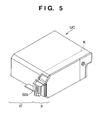
- FIG. 5 is an external perspective view showing the configuration of a head cartridge IJC in which an ink tank and a printhead have been formed as a single body;
- FIG. 6 shows a double-ended signal A and a single-ended signal B prior to being superimposed.
- FIG. 7 shows a differential input circuit and superimposed input signals
- FIG. 8 is a block diagram of a head controller and printhead of the main body of a printing apparatus with a differential input circuit and a logic circuit configured on separate element substrates;
- FIG. 9 is a timing chart of signals in which a DATA signal and a CLK signal transferred to a printhead are double-ended signals, and superimposed on an LT signal and an HE signal;
- FIG. 10 is a block diagram of a head controller and printhead of the main body of a printing apparatus with a differential input circuit and a logic circuit configured on the same element substrate;
- FIG. 11 shows a differential input circuit and superimposed input signals.
- a printing apparatus is described, by way of example, that uses a printhead according to an inkjet system.
- the terms "print” and “printing” not only include the formation of significant information such as characters and graphics, but also broadly include the formation of images, figures, patterns, and the like on a print medium, or the processing of the medium, regardless of whether they are significant or insignificant and whether they are so visualized as to be visually perceivable by humans.
- the term "print medium” not only includes a paper sheet used in common printing apparatuses, but also broadly includes materials, such as cloth, a plastic film, a metal plate, glass, ceramics, wood, and leather, capable of accepting ink.
- ink includes a liquid which, when applied onto a print medium, can form images, figures, patterns, and the like, can process the print medium, and can process ink (e.g., can solidify or insolubilize a coloring agent contained in ink applied to the print medium).
- printing element broadly includes a discharge orifice and a fluid path in communication with that orifice, and an element that generates energy used for ink discharge.
- element substrate used in this description indicates not simply a base constituted from a silicon semiconductor, but a base provided with elements, wiring, and the like. "On the element substrate” indicates not only on the surface of the element substrate, but may also refer to being on the surface of the element substrate or to being inside an element base in the vicinity of the surface of the element substrate. Also, the term “built-in” used in the invention is a term indicating not merely that separate elements are simply disposed on the base; this term indicates that elements are manufactured formed integrated on the element substrate with a semiconductor circuit manufacturing process or the like.
- FIG. 3 is an outer perspective view showing an overview of the configuration of an inkjet printing apparatus 1 that is a typical embodiment of the present invention.
- a printhead 3 that performs printing by discharging ink according to an inkjet system is loaded in the inkjet printing apparatus (referred to below as a printing apparatus).
- a transmission mechanism 4 transmits driving force generated with a carriage motor M1 to a carriage 2 in which the printhead 3 is loaded, thus moving the carriage 2 back and forth in the direction of arrow A.
- a print medium P such as print paper is supplied via a paper supply mechanism 5 and transported to a printing position. At that printing position, printing is performed by discharging ink from the printhead 3 to the print medium P.
- Loaded in the carriage 2 of the printing apparatus 1 is not only the printhead 3, but also ink cartridges 6 that store ink supplied to the printhead 3.
- the ink cartridges 6 are removable from the carriage 2.
- the printing apparatus 1 shown in FIG. 3 is capable of color printing, and therefore four ink cartridges are loaded in the carriage 2 that respectively house magenta (M), cyan (C), yellow (Y), and black (K) inks. These four ink cartridges are each independently removable.
- the printhead 3 prints by selectively discharging ink from a plurality of discharge orifices, by applying energy according to a printing signal.
- an inkjet system is adopted in which ink is discharged using thermal energy, and the printhead 3 is provided with electrothermal transducers in order to generate thermal energy. Electrical energy applied to the electrothermal transducers is converted to thermal energy.
- An electrothermal transducer is provided corresponding to each of the discharge orifices, and ink is discharged from a corresponding discharge orifice by applying a pulse voltage to a corresponding electrothermal transducer according to a printing signal.
- An element substrate is disposed within the printhead, and the aforementioned electrothermal transducers are provided on the element substrate. Also provided on the element substrate are a shift register and a latch circuit that are logic circuits for selectively driving the electrothermal transducers, and a drive circuit and the like.
- image data from outside the printhead is serially input to the shift register according to a clock signal, and after undergoing parallel conversion, the image data is held in the latch circuit according to a latch signal.
- the drive circuit is configured with an AND circuit, a switching transistor, and the like, and selectively drives the electrothermal transducers according to the image data held in the latch circuit and a time division signal.
- the carriage 2 is linked to a portion of a drive belt 7 of the transmission mechanism 4 that transmits driving force of the carriage motor M1, and is guidably supported so as to be capable of sliding along a guide shaft 13 in the direction of arrow A. Accordingly, the carriage 2 moves back and forth along the guide shaft 13 due to forward and reverse rotation of the carriage motor M1. Also, a scale 8 is provided in order to indicate the position of the carriage 2 in the movement direction (the direction of arrow A) of the carriage 2.
- a platen (not shown) is provided in the printing apparatus 1 facing a discharge orifice face where the discharge orifices (not shown) of the printhead 3 are formed, and the carriage 2 loaded with the printhead 3 is moved back and forth by the driving force of the carriage motor M1. At the same time, by discharging ink by applying a printing signal to the printhead 3, printing is performed across the entire width of a print medium P that has been transported onto the platen.
- FIG. 4 is a block diagram showing the control configuration of the printing apparatus shown in FIG. 3.
- a controller 600 includes an MPU 601 and a ROM 602 in which a program corresponding to a control sequence described below, a required table, and other fixed data are stored.
- the controller 600 also includes an application specific integrated circuit (ASIC) 603 that generates control signals for control of the carriage motor M1, control of a transport motor M2, and control of the printhead 3.
- ASIC application specific integrated circuit
- the controller 600 also includes a RAM 604 provided with an image data decompression area and a work area for program execution.
- the controller 600 also includes a system bus 605 whereby the MPU 601, the ASIC 603, and the RAM 604 are connected to each other, and data transfer is performed.
- the controller 600 includes an A/D converter 606 that performs A/D conversion of an analog signal that has been input from a sensor group described below, and supplies a digital signal to the MPU 601.
- numeral 610 indicates a computer or the like that is a supply source of image data, referred to generally as a host apparatus.
- Image data, commands, status signals, and the like are transferred between the host apparatus 610 and the printing apparatus 1 via an interface (I/F) 611.
- I/F interface
- Numeral 620 indicates a switch group configured from switches or the like for receiving input of instructions from an operator, including a power switch 621, a print switch 622 for instructing print start, a recovery switch 623 for indicating to start recovery processing, and the like.
- Numeral 630 indicates a sensor group configured with a position sensor 631 such as a photocoupler, a temperature sensor 632, and the like.
- Numeral 640 indicates a carriage motor driver that drives the carriage motor M1
- numeral 642 indicates a transport motor driver that drives the transport motor M2.
- Numeral 644 indicates a printhead driver that drives the printhead 3.
- a logic signal may be, for example, a data signal (DATA), a clock signal (CLK), a latch signal (LT), or a heat enable signal (HE).
- the ink cartridges 6 and the printhead 3 can be separated, but an exchangeable head cartridge may also be configured in which the ink cartridges 6 and the printhead 3 are formed as a single body.
- FIG. 5 is an external perspective view showing the configuration of a head cartridge IJC in which an ink tank and a printhead have been formed as a single body.
- the dotted line K is a boundary line of an ink tank IT and a printhead 3.
- the head cartridge IJC is provided with an electrode (not shown) for receiving an electrical signal such as the aforementioned differential signal provided from the carriage 2 when the head cartridge IJC has been loaded in the carriage 2. With this electrical signal, the printhead 3 is driven to discharge ink as described above.
- numeral 500 indicates a line of ink discharge orifices.
- the differential input circuit is configured from resistors 409 and 411, MOSs 405 and 406, a constant current source 410, and buffers 407 and 408.
- a low voltage differential signal (a double-ended pulse signal) has been superimposed on a single-ended pulse signal.
- a signal A+ has been superimposed on a signal B
- a signal A- has been superimposed on the signal B.
- Electrothermal transducers are provided on the element substrate of the invention, and a shift register and a latch circuit that are logic circuits for selectively driving the electrothermal transducers, and a drive circuit and the like, are provided on the element substrate.
- the printhead performs printing based on the image data, and the image data is serially input to the shift register according to the clock signal. After undergoing parallel conversion, the image data is held in the latch circuit according to a latch signal.
- the drive circuit selectively drives the electrothermal transducers according to a time determined from a heat enable signal, the image data held in the latch circuit, and a time-division signal.
- the amplitude of the superimposed double-ended signals is not particularly limited as long as the amplitude is not greater than the driving voltage of the logic circuit.
- the logic circuit is configured with a shift register, a latch circuit, and the like.
- the amplitude of the single-ended signal on which the low voltage differential signal is superimposed is a voltage of about half the driving voltage of the logic circuit.
- the input superimposed signal has an amplitude that does not exceed a differential input voltage range.
- the superimposed signals 401 and 402 satisfying the above conditions are respectively input to IN+ and IN-, which are input pads of the differential input circuit (FIG. 7) used in this example.
- the signals are respectively input to the gates of the MOSs 405 and 406.
- the MOS 405 When the difference between the signals 401 and 402 is positive, the MOS 405 is ON, and the MOS 406 is OFF. A low level signal is output to an OUT1. Conversely when the difference between the signals 401 and 402 is negative, the MOS 405 is OFF, so a high level signal is output to the OUT1.
- the output signal is shaped by the buffer 407 to have a waveform like the signal 403.
- the signal output from an OUT2 is obtained by adding together the signals input to the input pads IN+ and IN-, so the concavities and convexities in the respective signals are filled in, and due to subsequent shaping by the buffer 408, the signal output from the OUT2 has a waveform like the signal 404.
- the output signal from the OUT2 being a signal in which superimposed signals are disassembled, is a signal in which the superimposed signals 401 and 402 are added, so unlike the signal output from the OUT1, the signal output from the OUT2 is mixed with noise generated, for example, in the signal transfer path to the printhead.
- an inverter of the output signal of the OUT2 is provided with a hysteresis property, and thus the configuration is robust with respect to noise.
- FIG. 8 shows a block diagram of this example.
- the drawing is simplified by extracting only the part related to signal transmission, that is a distinguishing characteristic of the invention, and shows the controller 600 included in the main body of the printing apparatus, and the element substrate used to configure the printhead 3.
- a signal obtained by superimposing two or more logic signals is output from the controller 600 of the main body of the printing apparatus.
- a logic circuit 504 includes a heater array constituting a printing element and a drive circuit for the heater array, a latch circuit, and a shift register that are formed on the same element substrate.
- a differential input circuit 503 is the differential input circuit shown in FIG. 7, and is formed on a separate substrate from the logic circuit 504.
- the hysteresis output configuration shown in FIG. 11 may be adopted for a portion of an LT signal output stage in a circuit structure that is subjected to logic reversal due to noise.
- signals to be superimposed are high frequency signals such as a DATA signal and a CLK signal.
- INA+ and INA- are signals in which a DATA signal is superimposed on an LT signal (three logic signals, namely a DATA+ signal, a DATA-signal, and an LT signal, become a superimposed signal in which the DATA+ signal is superimposed on the LT signal (INA+), and a superimposed signal in which the DATA- signal is superimposed on the LT signal (INA-)).
- INB+ and INB- are signals in which a CLK signal is superimposed on an HE signal (three logic signals, namely a CLK+ signal, a CLK- signal, and an HE signal, become a superimposed signal in which the CLK+ signal is superimposed on the HE signal (INB+), and a superimposed signal in which the CLK- signal is superimposed on the HE signal (INB-)).
- These signals are transferred via differential data transfer that has excellent robustness with respect to noise, and little electromagnetic radiation, and input to the differential input circuit 503. After being respectively converted into a DATA signal, an LT signal, a CLK signal, and an HE signal, these signals are input to a terminal of a conventional printing element, and connected to the shift register 105, the latch circuit 106, and the drive circuit 107, which are logic circuits.
- FIG. 10 is a block diagram showing the characteristics of Example 2 of the invention.
- the logic circuit 504 includes a heater array constituting a printing element and a drive circuit for the heater array, a latch circuit, and a shift register, and on the same substrate 502, the same differential input circuit 503 as in Example 1 is configured.
- the hysteresis output configuration shown in FIG. 11 may be adopted for a portion of an LT signal output stage in a circuit structure that is subjected to logic reversal due to noise.
- a means for generating thermal energy as energy used for allowing ink discharge to be performed, and by employing a system in which a change in the state of ink is caused using that thermal energy, greater density and greater definition are attainable.
- a means for generating thermal energy for example, an electrothermal transducer or the like may be used.
- a printing apparatus other than an apparatus provided integrated or separately as an image output terminal of an information processing device such as a computer, an embodiment of a copy apparatus combined with a reader or the like may also be adopted. Further, an embodiment of a facsimile apparatus having send-receive functions may also be adopted.
Landscapes
- Engineering & Computer Science (AREA)
- Theoretical Computer Science (AREA)
- Human Computer Interaction (AREA)
- Physics & Mathematics (AREA)
- General Engineering & Computer Science (AREA)
- General Physics & Mathematics (AREA)
- Particle Formation And Scattering Control In Inkjet Printers (AREA)
- Ink Jet (AREA)
- Electronic Switches (AREA)
Abstract
Description
- The present invention relates to a printhead, a head cartridge, and a printing apparatus employing either of the printhead and the head cartridge, suitable for use in inkjet printing in which ink droplets are discharged.
- An inkjet printing apparatus is configured so as to print information on a print medium by discharging printing ink from a plurality of fine nozzles of a printhead according to a print signal. An inkjet printing apparatus has advantages such as being capable of non-contact printing to a print medium such as print paper, easy conversion to color, and being abundantly quiet.
- FIG. 1 is a block diagram showing a circuit configuration in a conventional printhead, and an example timing chart of signals transmitted to the printhead from a printing apparatus.
- A DATA signal 101 (digital signal: image data) is serially input to a
shift register 105 in synchronization with the edges of a CLK signal 102 (clock signal). Theshift register 105 temporarily stores data that has been input, the data corresponding to heaters. - Next, when an LT signal 103 (latch signal) that is input to a
latch circuit 106 goes low, the data stored in theshift register 105 is latched in thelatch circuit 106. When the LT signal 103 goes high, the data latched in thelatch circuit 106 is held. - When an HE signal 104 (heat enable signal) is input to a
drive circuit 107 in a state with data being held, electric current flows to a heater corresponding to the data according to time, at a timing when theHE signal 104 goes low. - Printing is performed by repeatedly performing the above sort of data transfer and printhead driving.
- On the other hand, at present, increased performance such as faster speed is sought for inkjet printing apparatuses. Thus, as a means for increasing printing speed, there are methods wherein the cycle in which ink is discharged from the nozzles is shortened. However, there are problems such as the fact that due to shortening that cycle, many signals are transmitted with high frequency, and thus there is an effect from radiated electromagnetic waves.
- Also, in a thermal inkjet printing apparatus, in addition to a signal, a high current that is allowed to flow to a heater flows to the printhead by being transmitted through a long flexible cable or the like from the main body of the printing apparatus, and noise generated by this current interferes with the signal. There is a risk this will lead to malfunction of the head. Thus, it is necessary for a thermal inkjet printing apparatus to be robust with respect to noise caused by this current.
- Consequently, a differential input circuit has been disclosed as one way of dealing with these problems (see
Japanese Patent Publication Laid-open No. 10-166583 - In
Japanese Patent Publication Laid-open No. 10-166583 - Because the double-ended signals use the differential of the +/- signals, they can be transferred as signals with a smaller voltage amplitude than in the case of a conventional single-ended signal. Thus the electromagnetic radiation of those double-ended signals is less than when transmitting with a single-ended signal. Also, because these signals pass through a flexible cable or the like adjacent to each other, electromagnetic noise generated from the current of each signal is cancelled by the other, thus suppressing interference with the other signal.
- Thus, electromagnetic radiation during high frequency signal transmission, which was a problem for accelerating printing speed, can be suppressed by adopting differential data transfer.
- Also, differential data transfer is very robust with respect to external noise. Because a double-ended signal uses the differential of the +/signals, even if external noise is applied, the differential does not change provided that the same noise is applied to both the + and - signals, so the effect of noise can be ignored.
- Thus, robustness with respect to noise caused by high current flowing to a heater is insured, so it is possible to prevent malfunction of the head.
- However, because it is necessary with differential data transfer to use two signal lines to transfer signals conventionally transferred with one signal line, such a configuration leads to increased size of the apparatus and also increased costs, due to an increased number of input pads and an accompanying increase in wiring.
- So, there is a desire to reduce the number of input pads, suppressing an increase in the number of input pads and an accompanying increased size and cost of the apparatus, while making use of the advantages of employing a differential input circuit.
- The present invention is directed to a printhead, a head cartridge, and a printing apparatus.
- A printhead, a head cartridge, or a printing apparatus in which either is used according to this invention is capable of minimizing increased size and cost of the apparatus by reducing the number of input pads, while making use of the advantages of employing a differential input circuit.
- According to one aspect of the present invention, a printhead includes a logic circuit configured to drive a plurality of print elements with a plurality of logic signals, a differential input circuit configured to generate the plurality of logic signals in order to drive the logic circuit based on a differential signal input from outside; and an input pad to which the differential signal obtained by superimposing two or more logic signals is input. The differential input circuit includes a disassembling circuit that disassembles the differential signal input via the input pad into separate logic signals.
- According to another aspect of the present invention, a head cartridge includes a printhead having a logic circuit configured to drive a plurality of print elements with a plurality of logic signals, and a differential input circuit configured to generate the plurality of logic signals in order to drive said logic circuit based on a differential signal input from outside; an ink tank in which ink is encapsulated; and an input pad to which the differential signal obtained by superimposing two or more logic signals is input. The differential input circuit includes a disassembling circuit that disassembles the differential signal input via the input pad into separate logic signals.
- According to still another aspect of the present invention, a printing apparatus that performs printing using the printhead or the head cartridge, includes a first generating unit configured to generate three or more differing logic signals; a second generating unit configured to generate a differential signal obtained by superimposing at least two differing logic signals, using the three or more differing logic signals; and an output unit outputting the differential signal generated by the second generating unit to the printhead.
- Further features of the present invention will become apparent from the following description of exemplary embodiments (with reference to the attached drawings).
- FIG. 1 is a block diagram showing a circuit diagram of a conventional printhead and a timing chart of signals transmitted to the printhead from a printing apparatus;
- FIG. 2 is a timing chart of signals input to a differential input circuit;
- FIG. 3 is an outer perspective view showing an overview of the configuration of an inkjet printing apparatus that is a typical embodiment of the present invention;
- FIG. 4 is a block diagram showing the configuration of a control circuit of the printing apparatus;
- FIG. 5 is an external perspective view showing the configuration of a head cartridge IJC in which an ink tank and a printhead have been formed as a single body;
- FIG. 6 shows a double-ended signal A and a single-ended signal B prior to being superimposed.
- FIG. 7 shows a differential input circuit and superimposed input signals;
- FIG. 8 is a block diagram of a head controller and printhead of the main body of a printing apparatus with a differential input circuit and a logic circuit configured on separate element substrates;
- FIG. 9 is a timing chart of signals in which a DATA signal and a CLK signal transferred to a printhead are double-ended signals, and superimposed on an LT signal and an HE signal;
- FIG. 10 is a block diagram of a head controller and printhead of the main body of a printing apparatus with a differential input circuit and a logic circuit configured on the same element substrate; and
- FIG. 11 shows a differential input circuit and superimposed input signals.
- In the examples described below, a printing apparatus is described, by way of example, that uses a printhead according to an inkjet system.
- In this specification, the terms "print" and "printing" not only include the formation of significant information such as characters and graphics, but also broadly include the formation of images, figures, patterns, and the like on a print medium, or the processing of the medium, regardless of whether they are significant or insignificant and whether they are so visualized as to be visually perceivable by humans.
- Also, the term "print medium" not only includes a paper sheet used in common printing apparatuses, but also broadly includes materials, such as cloth, a plastic film, a metal plate, glass, ceramics, wood, and leather, capable of accepting ink.
- Furthermore, the term "ink" (to be also referred to as a "liquid" hereinafter) should be extensively interpreted similar to the definition of "print" described above. That is, "ink" includes a liquid which, when applied onto a print medium, can form images, figures, patterns, and the like, can process the print medium, and can process ink (e.g., can solidify or insolubilize a coloring agent contained in ink applied to the print medium).
- Moreover, the term "printing element", if not specifically stated otherwise, broadly includes a discharge orifice and a fluid path in communication with that orifice, and an element that generates energy used for ink discharge.
- The term "element substrate" used in this description indicates not simply a base constituted from a silicon semiconductor, but a base provided with elements, wiring, and the like. "On the element substrate" indicates not only on the surface of the element substrate, but may also refer to being on the surface of the element substrate or to being inside an element base in the vicinity of the surface of the element substrate. Also, the term "built-in" used in the invention is a term indicating not merely that separate elements are simply disposed on the base; this term indicates that elements are manufactured formed integrated on the element substrate with a semiconductor circuit manufacturing process or the like.
- FIG. 3 is an outer perspective view showing an overview of the configuration of an
inkjet printing apparatus 1 that is a typical embodiment of the present invention. - As shown in FIG. 3, a
printhead 3 that performs printing by discharging ink according to an inkjet system is loaded in the inkjet printing apparatus (referred to below as a printing apparatus). Atransmission mechanism 4 transmits driving force generated with a carriage motor M1 to acarriage 2 in which theprinthead 3 is loaded, thus moving thecarriage 2 back and forth in the direction of arrow A. Along with this back and forth movement, for example, a print medium P such as print paper is supplied via apaper supply mechanism 5 and transported to a printing position. At that printing position, printing is performed by discharging ink from theprinthead 3 to the print medium P. - Loaded in the
carriage 2 of theprinting apparatus 1 is not only theprinthead 3, but alsoink cartridges 6 that store ink supplied to theprinthead 3. Theink cartridges 6 are removable from thecarriage 2. - The
printing apparatus 1 shown in FIG. 3 is capable of color printing, and therefore four ink cartridges are loaded in thecarriage 2 that respectively house magenta (M), cyan (C), yellow (Y), and black (K) inks. These four ink cartridges are each independently removable. - The joining faces of the
carriage 2 and theprinthead 3 are appropriately placed in contact, so that it is possible to achieve and maintain a required electrical connection. Theprinthead 3 prints by selectively discharging ink from a plurality of discharge orifices, by applying energy according to a printing signal. In particular, in theprinthead 3 in this example, an inkjet system is adopted in which ink is discharged using thermal energy, and theprinthead 3 is provided with electrothermal transducers in order to generate thermal energy. Electrical energy applied to the electrothermal transducers is converted to thermal energy. Using a pressure change that occurs due to the growth and contraction of bubbles due to film boiling that occurs due to application of the thermal energy to the ink, the ink is discharged from the discharge orifices. An electrothermal transducer is provided corresponding to each of the discharge orifices, and ink is discharged from a corresponding discharge orifice by applying a pulse voltage to a corresponding electrothermal transducer according to a printing signal. - An element substrate is disposed within the printhead, and the aforementioned electrothermal transducers are provided on the element substrate. Also provided on the element substrate are a shift register and a latch circuit that are logic circuits for selectively driving the electrothermal transducers, and a drive circuit and the like.
- As described below, image data from outside the printhead is serially input to the shift register according to a clock signal, and after undergoing parallel conversion, the image data is held in the latch circuit according to a latch signal. The drive circuit is configured with an AND circuit, a switching transistor, and the like, and selectively drives the electrothermal transducers according to the image data held in the latch circuit and a time division signal.
- As shown in FIG. 3, the
carriage 2 is linked to a portion of a drive belt 7 of thetransmission mechanism 4 that transmits driving force of the carriage motor M1, and is guidably supported so as to be capable of sliding along aguide shaft 13 in the direction of arrow A. Accordingly, thecarriage 2 moves back and forth along theguide shaft 13 due to forward and reverse rotation of the carriage motor M1. Also, ascale 8 is provided in order to indicate the position of thecarriage 2 in the movement direction (the direction of arrow A) of thecarriage 2. - Also, a platen (not shown) is provided in the
printing apparatus 1 facing a discharge orifice face where the discharge orifices (not shown) of theprinthead 3 are formed, and thecarriage 2 loaded with theprinthead 3 is moved back and forth by the driving force of the carriage motor M1. At the same time, by discharging ink by applying a printing signal to theprinthead 3, printing is performed across the entire width of a print medium P that has been transported onto the platen. - FIG. 4 is a block diagram showing the control configuration of the printing apparatus shown in FIG. 3.
- As shown in FIG. 4, a
controller 600 includes anMPU 601 and aROM 602 in which a program corresponding to a control sequence described below, a required table, and other fixed data are stored. Thecontroller 600 also includes an application specific integrated circuit (ASIC) 603 that generates control signals for control of the carriage motor M1, control of a transport motor M2, and control of theprinthead 3. Thecontroller 600 also includes aRAM 604 provided with an image data decompression area and a work area for program execution. Thecontroller 600 also includes asystem bus 605 whereby theMPU 601, theASIC 603, and theRAM 604 are connected to each other, and data transfer is performed. Further, thecontroller 600 includes an A/D converter 606 that performs A/D conversion of an analog signal that has been input from a sensor group described below, and supplies a digital signal to theMPU 601. - Also, in FIG. 4, numeral 610 indicates a computer or the like that is a supply source of image data, referred to generally as a host apparatus. Image data, commands, status signals, and the like are transferred between the
host apparatus 610 and theprinting apparatus 1 via an interface (I/F) 611. -
Numeral 620 indicates a switch group configured from switches or the like for receiving input of instructions from an operator, including apower switch 621, aprint switch 622 for instructing print start, arecovery switch 623 for indicating to start recovery processing, and the like.Numeral 630 indicates a sensor group configured with aposition sensor 631 such as a photocoupler, atemperature sensor 632, and the like. -
Numeral 640 indicates a carriage motor driver that drives the carriage motor M1, and numeral 642 indicates a transport motor driver that drives the transport motor M2.Numeral 644 indicates a printhead driver that drives theprinthead 3. - The
ASIC 603 and theMPU 601 of thecontroller 600 of the main body of the printing apparatus, and theprinthead driver 644, each independently create a differential signal in which two or more logic signals are superimposed. Also, theASIC 603, theMPU 601, and theprinthead driver 644, in multiple cooperation, create a differential signal in which two or more logical signals have been superimposed. When performing printing scanning with theprinthead 3, these differential signals are transferred to the differential input circuit of theprinthead 3 while directly accessing a storage area of theRAM 604. Specifically, for example, three or more logic signals are created with theASIC 603, these logic signals are made into two superimposed signals that become a differential signal with theprinthead driver 644, and this differential signal is transferred to the differential input circuit of theprinthead 3. Here, a logic signal may be, for example, a data signal (DATA), a clock signal (CLK), a latch signal (LT), or a heat enable signal (HE). - In the configuration shown in FIG. 3, the
ink cartridges 6 and theprinthead 3 can be separated, but an exchangeable head cartridge may also be configured in which theink cartridges 6 and theprinthead 3 are formed as a single body. - FIG. 5 is an external perspective view showing the configuration of a head cartridge IJC in which an ink tank and a printhead have been formed as a single body. In FIG. 5, the dotted line K is a boundary line of an ink tank IT and a
printhead 3. The head cartridge IJC is provided with an electrode (not shown) for receiving an electrical signal such as the aforementioned differential signal provided from thecarriage 2 when the head cartridge IJC has been loaded in thecarriage 2. With this electrical signal, theprinthead 3 is driven to discharge ink as described above. - In FIG. 5, numeral 500 indicates a line of ink discharge orifices.
- Next, a more detailed description is given by way of a specific example.
- Following is a description of the differential input circuit and differential signal used in this example, provided in the form of an element substrate, with reference to the example in FIG. 7. The differential input circuit is configured from
resistors MOSs current source 410, and buffers 407 and 408. In an input signal, a low voltage differential signal (a double-ended pulse signal) has been superimposed on a single-ended pulse signal. As shown in FIG. 6, in asignal 401, a signal A+ has been superimposed on a signal B, and in asignal 402, a signal A- has been superimposed on the signal B. - Electrothermal transducers are provided on the element substrate of the invention, and a shift register and a latch circuit that are logic circuits for selectively driving the electrothermal transducers, and a drive circuit and the like, are provided on the element substrate. The printhead performs printing based on the image data, and the image data is serially input to the shift register according to the clock signal. After undergoing parallel conversion, the image data is held in the latch circuit according to a latch signal. The drive circuit selectively drives the electrothermal transducers according to a time determined from a heat enable signal, the image data held in the latch circuit, and a time-division signal.
- The amplitude of the superimposed double-ended signals is not particularly limited as long as the amplitude is not greater than the driving voltage of the logic circuit. In this example, the potential of the single-ended pulse signal on which a low voltage differential signal is superimposed is used as a central potential, and the signal has a signal amplitude of about Vp-p=200mV. The logic circuit is configured with a shift register, a latch circuit, and the like.
- Also, the amplitude of the single-ended signal on which the low voltage differential signal is superimposed is a voltage of about half the driving voltage of the logic circuit.
- The input superimposed signal has an amplitude that does not exceed a differential input voltage range.
- The superimposed signals 401 and 402 satisfying the above conditions are respectively input to IN+ and IN-, which are input pads of the differential input circuit (FIG. 7) used in this example.
- The signals are respectively input to the gates of the
MOSs signals MOS 405 is ON, and theMOS 406 is OFF. A low level signal is output to an OUT1. Conversely when the difference between thesignals MOS 405 is OFF, so a high level signal is output to the OUT1. - The output signal is shaped by the
buffer 407 to have a waveform like thesignal 403. On the other hand, the signal output from an OUT2 is obtained by adding together the signals input to the input pads IN+ and IN-, so the concavities and convexities in the respective signals are filled in, and due to subsequent shaping by thebuffer 408, the signal output from the OUT2 has a waveform like thesignal 404. - By using a differential input circuit as shown in FIG. 7 in the above manner, it is possible to reduce the three pads in the case of not using a differential signal (signal A+ pad, signal A- pad, and signal B pad) to two pads (IN+, IN-).
- Next, in FIG. 7, the output signal from the OUT2, being a signal in which superimposed signals are disassembled, is a signal in which the superimposed
signals - In the case of an analog signal such as a heat enable signal (HE) that determines the driving time of a heater, there is no actual effect even if noise is mixed into the signal, but in the case of a logic signal, logic may be reversed by noise. In order to prevent such a reversal of logic, in the configuration shown in FIG. 11, an inverter of the output signal of the OUT2 is provided with a hysteresis property, and thus the configuration is robust with respect to noise.
- FIG. 8 shows a block diagram of this example.
- Here, the drawing is simplified by extracting only the part related to signal transmission, that is a distinguishing characteristic of the invention, and shows the
controller 600 included in the main body of the printing apparatus, and the element substrate used to configure theprinthead 3. - A signal obtained by superimposing two or more logic signals is output from the
controller 600 of the main body of the printing apparatus. - A
logic circuit 504 includes a heater array constituting a printing element and a drive circuit for the heater array, a latch circuit, and a shift register that are formed on the same element substrate. Adifferential input circuit 503 is the differential input circuit shown in FIG. 7, and is formed on a separate substrate from thelogic circuit 504. The hysteresis output configuration shown in FIG. 11 may be adopted for a portion of an LT signal output stage in a circuit structure that is subjected to logic reversal due to noise. - Signals INA+, INA-, and INB+, INB- that are input to the
printhead 3 are shown in FIG. 9. - It is desirable that signals to be superimposed (made double-ended) are high frequency signals such as a DATA signal and a CLK signal. By making these signals double-ended, it is possible to further anticipate results such as suppression of electromagnetic radiation and improvement of robustness with respect to noise in signal transfer between the
controller 600 and theprinthead 3. - In this example, INA+ and INA- are signals in which a DATA signal is superimposed on an LT signal (three logic signals, namely a DATA+ signal, a DATA-signal, and an LT signal, become a superimposed signal in which the DATA+ signal is superimposed on the LT signal (INA+), and a superimposed signal in which the DATA- signal is superimposed on the LT signal (INA-)). INB+ and INB- are signals in which a CLK signal is superimposed on an HE signal (three logic signals, namely a CLK+ signal, a CLK- signal, and an HE signal, become a superimposed signal in which the CLK+ signal is superimposed on the HE signal (INB+), and a superimposed signal in which the CLK- signal is superimposed on the HE signal (INB-)).
- These signals are transferred via differential data transfer that has excellent robustness with respect to noise, and little electromagnetic radiation, and input to the
differential input circuit 503. After being respectively converted into a DATA signal, an LT signal, a CLK signal, and an HE signal, these signals are input to a terminal of a conventional printing element, and connected to theshift register 105, thelatch circuit 106, and thedrive circuit 107, which are logic circuits. - In the above manner, in this example, it is possible to reduce the six input pads from the DATA+ signal, the DATA- signal, the LT signal, the CLK+ signal, the CLK- signal, and the LT signal to the four input pads from the signals INA+, INA-, INB+, and INB-. Also, in this example, by providing the logic circuit and the differential input circuit on separate substrates, there is more freedom with respect to arrangement of the respective substrates, and also arrangement of connectors and wiring and the like, resulting in increased freedom of design.
- In this example, unlike in Example 1, a configuration is provided in which the differential input circuit and the logic circuit are on the same substrate.
- FIG. 10 is a block diagram showing the characteristics of Example 2 of the invention.
- In this example, the data and timing charts of that data are the same as in Example 1, so a description thereof is omitted here.
- The
logic circuit 504 includes a heater array constituting a printing element and a drive circuit for the heater array, a latch circuit, and a shift register, and on thesame substrate 502, the samedifferential input circuit 503 as in Example 1 is configured. The hysteresis output configuration shown in FIG. 11 may be adopted for a portion of an LT signal output stage in a circuit structure that is subjected to logic reversal due to noise. - In the above manner, in this example, it is possible to reduce the six input pads from the DATA+ signal, the DATA- signal, the LT signal, the CLK+ signal, the CLK- signal, and the LT signal to the four input pads from the signals INA+, INA-, INB+, and INB-. Also, by adopting this configuration, reduced cost is possible due to a reduction in the number of components, a reduction in the total print substrate size, and the like.
- In the above examples, a means is provided for generating thermal energy as energy used for allowing ink discharge to be performed, and by employing a system in which a change in the state of ink is caused using that thermal energy, greater density and greater definition are attainable. As a means for generating thermal energy, for example, an electrothermal transducer or the like may be used.
- In addition, as an embodiment of a printing apparatus according to the invention, other than an apparatus provided integrated or separately as an image output terminal of an information processing device such as a computer, an embodiment of a copy apparatus combined with a reader or the like may also be adopted. Further, an embodiment of a facsimile apparatus having send-receive functions may also be adopted.
- With the invention, as described above, it is possible to attain transfer of a high frequency clock signal, a high frequency data signal, and the like necessary for realizing high speed driving of the printhead, while suppressing the effects of electromagnetic radiation or the like.
- Also, when these high frequency signals pass through a comparatively long flexible cable, electromagnetic radiation becomes a problem. With the invention, it is possible to suppress effects due to reducing the voltage amplitude of transmission signals.
- Also, with the invention, by superimposing two or more logic signals, in the above differential data transfer, it is possible to suppress an increase in the number of transmitted signals, the number of input signals, the number of input terminals, and the like.
- While the present invention has been described with reference to exemplary embodiments, it is to be understood that the invention is not limited to the disclosed exemplary embodiments. The scope of the following claims is to be accorded the broadest interpretation so as to encompass all such modifications and equivalent structures and functions.
Claims (11)
- A printhead (3) comprising:a logic circuit (105, 106, 107) configured to drive a plurality of print elements with a plurality of logic signals;a differential input circuit (503) configured to generate the plurality of logic signals in order to drive the logic circuit (105, 106, 107) based on a differential signal input from outside; andan input pad to which the differential signal obtained by superimposing two or more logic signals is input, wherein
the differential input circuit (503) includes a disassembling circuit that disassembles the differential signal input via the input pad into separate logic signals. - The printhead (3) according to claim 1, wherein the differential signal is obtained by superimposing a high frequency logic signal on a low frequency logic signal.
- The printhead (3) according to claim 2, wherein the high frequency logic signal is a clock signal (102), and the low frequency logic signal is a heat enable signal (104).
- The printhead (3) according to claim 2, wherein the high frequency logic signal is a data signal (101), and the low frequency logic signal is a latch signal (103).
- The printhead (3) according to any one of claims 1 to 4, wherein the logic circuit (105, 106, 107) includes a shift register (105) into which are input a clock signal (102) and a data signal (101) transmitted in synchronization with the clock signal (102).
- The printhead (3) according to any one of claims 1 to 5, wherein the differential input circuit (503) is formed on a separate substrate from the logic circuit (105, 106, 107).
- The printhead (3) according to any one of claims 1 to 5, wherein the differential input circuit (503) is formed on the same substrate as the logic circuit (105, 106, 107).
- The printhead (3) according to any one of claims 1 to 7, wherein the printhead (3) is for inkjet use.
- The printhead (3) according to claim 2, wherein the printhead (3) is for use in a thermal inkjet printing apparatus that performs ink foaming and discharge with thermal energy generated by current applied to an electrothermal transducer.
- A head cartridge (IJC) comprising:a printhead (3) including a logic circuit (105, 106, 107) configured to drive a plurality of print elements with a plurality of logic signals, and a differential input circuit (503) configured to generate the plurality of logic signals in order to drive said logic circuit (105, 106, 107) based on a differential signal input from outside;an ink tank (IT) in which ink is encapsulated; andan input pad to which the differential signal obtained by superimposing two or more logic signals is input, wherein
the differential input circuit (503) includes a disassembling circuit that disassembles the differential signal input via the input pad into separate logic signals. - A printing apparatus that performs printing using the printhead (3) according to any one of claims 1 to 9 or the head cartridge (IJC) according to claim 10, the printing apparatus comprising:a first generating unit configured to generate three or more differing logic signals;a second generating unit configured to generate a differential signal obtained by superimposing at least two differing logic signals, using the three or more differing logic signals; andan output unit outputting the differential signal generated by the second generating unit to the printhead (3).
Applications Claiming Priority (1)
| Application Number | Priority Date | Filing Date | Title |
|---|---|---|---|
| JP2006178585A JP4799292B2 (en) | 2006-06-28 | 2006-06-28 | Recording head, head cartridge, and recording apparatus using any of these |
Publications (3)
| Publication Number | Publication Date |
|---|---|
| EP1872948A2 true EP1872948A2 (en) | 2008-01-02 |
| EP1872948A3 EP1872948A3 (en) | 2009-07-29 |
| EP1872948B1 EP1872948B1 (en) | 2010-09-08 |
Family
ID=38420658
Family Applications (1)
| Application Number | Title | Priority Date | Filing Date |
|---|---|---|---|
| EP07012521A Not-in-force EP1872948B1 (en) | 2006-06-28 | 2007-06-26 | Printhead, head cartridge, and printing apparatus employing either of same |
Country Status (6)
| Country | Link |
|---|---|
| US (1) | US7959243B2 (en) |
| EP (1) | EP1872948B1 (en) |
| JP (1) | JP4799292B2 (en) |
| KR (1) | KR100916860B1 (en) |
| CN (1) | CN101096140B (en) |
| DE (1) | DE602007008979D1 (en) |
Cited By (2)
| Publication number | Priority date | Publication date | Assignee | Title |
|---|---|---|---|---|
| US8610867B2 (en) | 2008-01-21 | 2013-12-17 | Samsung Display Co., Ltd. | Liquid crystal display and liquid crystal composition included therein |
| US9341896B2 (en) | 2008-01-21 | 2016-05-17 | Samsung Display Co., Ltd. | Liquid crystal display |
Families Citing this family (5)
| Publication number | Priority date | Publication date | Assignee | Title |
|---|---|---|---|---|
| WO2010004742A1 (en) * | 2008-07-11 | 2010-01-14 | セイコーエプソン株式会社 | Liquid container, liquid jetting apparatus and liquid jetting system |
| CN101722729B (en) * | 2008-10-13 | 2012-03-07 | 北京美科艺数码科技发展有限公司 | Method and device for transmitting data between main board and spray nozzle panel of ink-jet printer |
| CN103328218B (en) | 2011-01-25 | 2015-09-30 | 惠普发展公司,有限责任合伙企业 | Print head apparatus, printer system and printhead built-in testing method |
| JP6950217B2 (en) * | 2017-03-22 | 2021-10-13 | セイコーエプソン株式会社 | Liquid discharge device |
| CN113165389A (en) * | 2018-12-03 | 2021-07-23 | 惠普发展公司,有限责任合伙企业 | Logic circuitry packaging |
Family Cites Families (13)
| Publication number | Priority date | Publication date | Assignee | Title |
|---|---|---|---|---|
| JPH10166583A (en) | 1996-12-16 | 1998-06-23 | Canon Inc | Recording head, recording head cartridge thereof, and recording apparatus using the recording head |
| JP2001121704A (en) * | 1999-10-26 | 2001-05-08 | Victor Co Of Japan Ltd | Image forming apparatus and method for image formation |
| JP3616546B2 (en) * | 2000-01-24 | 2005-02-02 | 株式会社沖データ | DRIVE CIRCUIT, PRINT HEAD USING THE SAME, ELECTROPHOTOGRAPHIC PRINTER, WIRING BOARD FOR DRIVE CIRCUIT, AND PRINT HEAD USING THE SAME |
| CN1179848C (en) * | 2000-12-08 | 2004-12-15 | 明基电通股份有限公司 | Control circuit for driving ink jet head in printing device |
| US6726298B2 (en) | 2001-02-08 | 2004-04-27 | Hewlett-Packard Development Company, L.P. | Low voltage differential signaling communication in inkjet printhead assembly |
| JP4666818B2 (en) * | 2001-06-15 | 2011-04-06 | キヤノン株式会社 | RECORDING HEAD, RECORDING HEAD CARTRIDGE, AND RECORDING DEVICE THEREOF |
| GB2407064B (en) * | 2001-07-25 | 2005-07-06 | Hewlett Packard Co | System for ink short protection |
| US6578940B2 (en) | 2001-07-25 | 2003-06-17 | Hewlett-Packard Development Company, L.P. | System for ink short protection |
| DE60223322T2 (en) * | 2001-08-31 | 2008-03-13 | Canon K.K. | Image printing device and associated control method |
| JP2005199665A (en) * | 2004-01-19 | 2005-07-28 | Canon Inc | Recording apparatus, recording head, and recording head substrate |
| KR20060067689A (en) * | 2004-12-15 | 2006-06-20 | 삼성전자주식회사 | Thermal transfer image forming apparatus and method using low voltage homogeneous signal transmission and reception method |
| JP4352019B2 (en) * | 2005-04-22 | 2009-10-28 | キヤノン株式会社 | Ink jet recording head and ink jet recording apparatus using the head |
| US7482837B2 (en) * | 2006-04-10 | 2009-01-27 | Atmel Corporation | System and method for combining signals on a differential I/O link |
-
2006
- 2006-06-28 JP JP2006178585A patent/JP4799292B2/en not_active Expired - Fee Related
-
2007
- 2007-06-18 US US11/764,705 patent/US7959243B2/en not_active Expired - Fee Related
- 2007-06-26 DE DE602007008979T patent/DE602007008979D1/en active Active
- 2007-06-26 EP EP07012521A patent/EP1872948B1/en not_active Not-in-force
- 2007-06-28 CN CN2007101270775A patent/CN101096140B/en not_active Expired - Fee Related
- 2007-06-28 KR KR1020070064250A patent/KR100916860B1/en not_active Expired - Fee Related
Cited By (2)
| Publication number | Priority date | Publication date | Assignee | Title |
|---|---|---|---|---|
| US8610867B2 (en) | 2008-01-21 | 2013-12-17 | Samsung Display Co., Ltd. | Liquid crystal display and liquid crystal composition included therein |
| US9341896B2 (en) | 2008-01-21 | 2016-05-17 | Samsung Display Co., Ltd. | Liquid crystal display |
Also Published As
| Publication number | Publication date |
|---|---|
| KR20080002641A (en) | 2008-01-04 |
| US20080001979A1 (en) | 2008-01-03 |
| DE602007008979D1 (en) | 2010-10-21 |
| CN101096140A (en) | 2008-01-02 |
| EP1872948A3 (en) | 2009-07-29 |
| KR100916860B1 (en) | 2009-09-09 |
| EP1872948B1 (en) | 2010-09-08 |
| CN101096140B (en) | 2010-08-25 |
| JP4799292B2 (en) | 2011-10-26 |
| JP2008006655A (en) | 2008-01-17 |
| US7959243B2 (en) | 2011-06-14 |
Similar Documents
| Publication | Publication Date | Title |
|---|---|---|
| JP4989433B2 (en) | Head substrate, recording head, head cartridge, and recording apparatus | |
| US7802858B2 (en) | Element board for printhead, printhead and printhead control method | |
| EP1872948B1 (en) | Printhead, head cartridge, and printing apparatus employing either of same | |
| EP1543972B1 (en) | Element board for printhead, and printhead having the same | |
| US7896469B2 (en) | Head substrate, printhead, head cartridge, and printing apparatus | |
| US7740333B2 (en) | Printhead, head cartridge, and printing apparatus using restriction circuit for restricting input of signals | |
| JP5032964B2 (en) | Head substrate, recording head, head cartridge, and recording apparatus | |
| JP2008279616A (en) | Recording apparatus and clock generation method | |
| KR100776973B1 (en) | Ink-jet printhead substrate, driving control method, ink-jet printhead and ink-jet printing apparatus | |
| US8857934B2 (en) | Print element substrate, printhead, and printing apparatus | |
| US8002370B2 (en) | Serial data transfer method, electric device, and printing apparatus | |
| JP5063314B2 (en) | Element substrate, recording head, head cartridge, and recording apparatus | |
| US7866798B2 (en) | Head cartridge, printhead, and substrate having downsized level conversion elements that suppress power consumption | |
| US20120212780A1 (en) | Printing apparatus and electronic device | |
| JP5906066B2 (en) | Head substrate, ink jet recording head using the head substrate, and recording apparatus using the recording head | |
| JP2021181220A (en) | Method for transmitting printing data and printer | |
| JP2008149494A (en) | Head substrate, recording head using the head substrate, and recording apparatus using the recording head | |
| JP2008155469A (en) | Substrate for liquid discharge head and liquid discharge head |
Legal Events
| Date | Code | Title | Description |
|---|---|---|---|
| PUAI | Public reference made under article 153(3) epc to a published international application that has entered the european phase |
Free format text: ORIGINAL CODE: 0009012 |
|
| AK | Designated contracting states |
Kind code of ref document: A2 Designated state(s): AT BE BG CH CY CZ DE DK EE ES FI FR GB GR HU IE IS IT LI LT LU LV MC MT NL PL PT RO SE SI SK TR |
|
| AX | Request for extension of the european patent |
Extension state: AL BA HR MK YU |
|
| PUAL | Search report despatched |
Free format text: ORIGINAL CODE: 0009013 |
|
| AK | Designated contracting states |
Kind code of ref document: A3 Designated state(s): AT BE BG CH CY CZ DE DK EE ES FI FR GB GR HU IE IS IT LI LT LU LV MC MT NL PL PT RO SE SI SK TR |
|
| AX | Request for extension of the european patent |
Extension state: AL BA HR MK RS |
|
| 17P | Request for examination filed |
Effective date: 20100129 |
|
| GRAP | Despatch of communication of intention to grant a patent |
Free format text: ORIGINAL CODE: EPIDOSNIGR1 |
|
| AKX | Designation fees paid |
Designated state(s): DE FR GB IT |
|
| GRAS | Grant fee paid |
Free format text: ORIGINAL CODE: EPIDOSNIGR3 |
|
| GRAA | (expected) grant |
Free format text: ORIGINAL CODE: 0009210 |
|
| AK | Designated contracting states |
Kind code of ref document: B1 Designated state(s): DE FR GB IT |
|
| REG | Reference to a national code |
Ref country code: GB Ref legal event code: FG4D |
|
| REF | Corresponds to: |
Ref document number: 602007008979 Country of ref document: DE Date of ref document: 20101021 Kind code of ref document: P |
|
| PG25 | Lapsed in a contracting state [announced via postgrant information from national office to epo] |
Ref country code: IT Free format text: LAPSE BECAUSE OF FAILURE TO SUBMIT A TRANSLATION OF THE DESCRIPTION OR TO PAY THE FEE WITHIN THE PRESCRIBED TIME-LIMIT Effective date: 20100908 |
|
| PLBE | No opposition filed within time limit |
Free format text: ORIGINAL CODE: 0009261 |
|
| STAA | Information on the status of an ep patent application or granted ep patent |
Free format text: STATUS: NO OPPOSITION FILED WITHIN TIME LIMIT |
|
| 26N | No opposition filed |
Effective date: 20110609 |
|
| REG | Reference to a national code |
Ref country code: DE Ref legal event code: R097 Ref document number: 602007008979 Country of ref document: DE Effective date: 20110609 |
|
| REG | Reference to a national code |
Ref country code: FR Ref legal event code: ST Effective date: 20120229 |
|
| PG25 | Lapsed in a contracting state [announced via postgrant information from national office to epo] |
Ref country code: FR Free format text: LAPSE BECAUSE OF NON-PAYMENT OF DUE FEES Effective date: 20110630 |
|
| PGFP | Annual fee paid to national office [announced via postgrant information from national office to epo] |
Ref country code: GB Payment date: 20200629 Year of fee payment: 14 |
|
| PGFP | Annual fee paid to national office [announced via postgrant information from national office to epo] |
Ref country code: DE Payment date: 20200827 Year of fee payment: 14 |
|
| REG | Reference to a national code |
Ref country code: DE Ref legal event code: R119 Ref document number: 602007008979 Country of ref document: DE |
|
| GBPC | Gb: european patent ceased through non-payment of renewal fee |
Effective date: 20210626 |
|
| PG25 | Lapsed in a contracting state [announced via postgrant information from national office to epo] |
Ref country code: GB Free format text: LAPSE BECAUSE OF NON-PAYMENT OF DUE FEES Effective date: 20210626 Ref country code: DE Free format text: LAPSE BECAUSE OF NON-PAYMENT OF DUE FEES Effective date: 20220101 |