EP1872101B1 - Sensor zur beseitigung unerwünschter komponenten und den sensor verwendendes messverfahren - Google Patents
Sensor zur beseitigung unerwünschter komponenten und den sensor verwendendes messverfahren Download PDFInfo
- Publication number
- EP1872101B1 EP1872101B1 EP06725573.7A EP06725573A EP1872101B1 EP 1872101 B1 EP1872101 B1 EP 1872101B1 EP 06725573 A EP06725573 A EP 06725573A EP 1872101 B1 EP1872101 B1 EP 1872101B1
- Authority
- EP
- European Patent Office
- Prior art keywords
- measurement
- light
- current
- charge storage
- detector
- Prior art date
- Legal status (The legal status is an assumption and is not a legal conclusion. Google has not performed a legal analysis and makes no representation as to the accuracy of the status listed.)
- Not-in-force
Links
- 238000005259 measurement Methods 0.000 title claims description 164
- 238000000034 method Methods 0.000 title claims description 45
- 238000003860 storage Methods 0.000 claims description 57
- 230000000737 periodic effect Effects 0.000 claims description 37
- 239000011159 matrix material Substances 0.000 claims description 33
- 239000000463 material Substances 0.000 claims description 32
- 239000008280 blood Substances 0.000 claims description 31
- 210000004369 blood Anatomy 0.000 claims description 31
- 238000000862 absorption spectrum Methods 0.000 claims description 27
- 238000007599 discharging Methods 0.000 claims description 21
- 238000000295 emission spectrum Methods 0.000 claims description 21
- 239000011888 foil Substances 0.000 claims description 18
- QVGXLLKOCUKJST-UHFFFAOYSA-N atomic oxygen Chemical compound [O] QVGXLLKOCUKJST-UHFFFAOYSA-N 0.000 claims description 16
- 230000017531 blood circulation Effects 0.000 claims description 16
- 239000001301 oxygen Substances 0.000 claims description 16
- 229910052760 oxygen Inorganic materials 0.000 claims description 16
- 239000011368 organic material Substances 0.000 claims description 14
- 230000036772 blood pressure Effects 0.000 claims description 6
- 238000005286 illumination Methods 0.000 claims description 4
- 239000000470 constituent Substances 0.000 claims description 3
- 230000001360 synchronised effect Effects 0.000 claims 1
- 206010052428 Wound Diseases 0.000 description 18
- 208000027418 Wounds and injury Diseases 0.000 description 18
- 239000003990 capacitor Substances 0.000 description 17
- 210000001519 tissue Anatomy 0.000 description 15
- 230000006870 function Effects 0.000 description 11
- 238000004519 manufacturing process Methods 0.000 description 11
- 238000013459 approach Methods 0.000 description 8
- 230000010354 integration Effects 0.000 description 8
- 241001465754 Metazoa Species 0.000 description 7
- 238000000691 measurement method Methods 0.000 description 6
- 206010020772 Hypertension Diseases 0.000 description 5
- 208000001953 Hypotension Diseases 0.000 description 5
- 230000008901 benefit Effects 0.000 description 5
- 210000004204 blood vessel Anatomy 0.000 description 5
- FJAOBQORBYMRNO-UHFFFAOYSA-N f16cupc Chemical compound [Cu+2].[N-]1C(N=C2C3=C(F)C(F)=C(F)C(F)=C3C(N=C3C4=C(F)C(F)=C(F)C(F)=C4C(=N4)[N-]3)=N2)=C(C(F)=C(F)C(F)=C2F)C2=C1N=C1C2=C(F)C(F)=C(F)C(F)=C2C4=N1 FJAOBQORBYMRNO-UHFFFAOYSA-N 0.000 description 5
- 208000012866 low blood pressure Diseases 0.000 description 5
- 230000003287 optical effect Effects 0.000 description 5
- 230000029663 wound healing Effects 0.000 description 5
- 238000003491 array Methods 0.000 description 4
- 238000010586 diagram Methods 0.000 description 4
- 230000008569 process Effects 0.000 description 4
- 239000000758 substrate Substances 0.000 description 4
- 230000001419 dependent effect Effects 0.000 description 3
- 230000008020 evaporation Effects 0.000 description 3
- 238000001704 evaporation Methods 0.000 description 3
- 230000004907 flux Effects 0.000 description 3
- 239000007789 gas Substances 0.000 description 3
- 238000007689 inspection Methods 0.000 description 3
- 230000007246 mechanism Effects 0.000 description 3
- 238000007639 printing Methods 0.000 description 3
- 238000004528 spin coating Methods 0.000 description 3
- 208000035143 Bacterial infection Diseases 0.000 description 2
- 238000010521 absorption reaction Methods 0.000 description 2
- 239000000853 adhesive Substances 0.000 description 2
- 230000001070 adhesive effect Effects 0.000 description 2
- 230000003321 amplification Effects 0.000 description 2
- 208000022362 bacterial infectious disease Diseases 0.000 description 2
- 239000002131 composite material Substances 0.000 description 2
- 238000001514 detection method Methods 0.000 description 2
- 239000003365 glass fiber Substances 0.000 description 2
- 230000035876 healing Effects 0.000 description 2
- 238000003384 imaging method Methods 0.000 description 2
- 239000007788 liquid Substances 0.000 description 2
- 238000003199 nucleic acid amplification method Methods 0.000 description 2
- 238000002106 pulse oximetry Methods 0.000 description 2
- 230000009467 reduction Effects 0.000 description 2
- 238000001228 spectrum Methods 0.000 description 2
- 108010054147 Hemoglobins Proteins 0.000 description 1
- 102000001554 Hemoglobins Human genes 0.000 description 1
- 108010064719 Oxyhemoglobins Proteins 0.000 description 1
- 208000004210 Pressure Ulcer Diseases 0.000 description 1
- 206010048038 Wound infection Diseases 0.000 description 1
- 238000009825 accumulation Methods 0.000 description 1
- 230000032683 aging Effects 0.000 description 1
- 238000004458 analytical method Methods 0.000 description 1
- 238000000149 argon plasma sintering Methods 0.000 description 1
- 230000009286 beneficial effect Effects 0.000 description 1
- 230000005540 biological transmission Effects 0.000 description 1
- 239000003086 colorant Substances 0.000 description 1
- 230000000052 comparative effect Effects 0.000 description 1
- 238000000151 deposition Methods 0.000 description 1
- 230000023077 detection of light stimulus Effects 0.000 description 1
- 230000000694 effects Effects 0.000 description 1
- 238000005516 engineering process Methods 0.000 description 1
- 238000005530 etching Methods 0.000 description 1
- 238000007667 floating Methods 0.000 description 1
- 230000001121 heart beat frequency Effects 0.000 description 1
- 208000015181 infectious disease Diseases 0.000 description 1
- 150000002500 ions Chemical class 0.000 description 1
- 239000002184 metal Substances 0.000 description 1
- 239000000203 mixture Substances 0.000 description 1
- 238000012544 monitoring process Methods 0.000 description 1
- 210000003205 muscle Anatomy 0.000 description 1
- 230000036284 oxygen consumption Effects 0.000 description 1
- 230000001681 protective effect Effects 0.000 description 1
- 238000001055 reflectance spectroscopy Methods 0.000 description 1
- 238000005070 sampling Methods 0.000 description 1
- 238000007789 sealing Methods 0.000 description 1
- 230000004083 survival effect Effects 0.000 description 1
- 238000012876 topography Methods 0.000 description 1
Images


Classifications
-
- G—PHYSICS
- G01—MEASURING; TESTING
- G01J—MEASUREMENT OF INTENSITY, VELOCITY, SPECTRAL CONTENT, POLARISATION, PHASE OR PULSE CHARACTERISTICS OF INFRARED, VISIBLE OR ULTRAVIOLET LIGHT; COLORIMETRY; RADIATION PYROMETRY
- G01J1/00—Photometry, e.g. photographic exposure meter
- G01J1/42—Photometry, e.g. photographic exposure meter using electric radiation detectors
- G01J1/44—Electric circuits
- G01J1/46—Electric circuits using a capacitor
-
- A—HUMAN NECESSITIES
- A61—MEDICAL OR VETERINARY SCIENCE; HYGIENE
- A61B—DIAGNOSIS; SURGERY; IDENTIFICATION
- A61B5/00—Measuring for diagnostic purposes; Identification of persons
- A61B5/145—Measuring characteristics of blood in vivo, e.g. gas concentration, pH value; Measuring characteristics of body fluids or tissues, e.g. interstitial fluid, cerebral tissue
- A61B5/1455—Measuring characteristics of blood in vivo, e.g. gas concentration, pH value; Measuring characteristics of body fluids or tissues, e.g. interstitial fluid, cerebral tissue using optical sensors, e.g. spectral photometrical oximeters
- A61B5/14551—Measuring characteristics of blood in vivo, e.g. gas concentration, pH value; Measuring characteristics of body fluids or tissues, e.g. interstitial fluid, cerebral tissue using optical sensors, e.g. spectral photometrical oximeters for measuring blood gases
- A61B5/14552—Details of sensors specially adapted therefor
-
- A—HUMAN NECESSITIES
- A61—MEDICAL OR VETERINARY SCIENCE; HYGIENE
- A61B—DIAGNOSIS; SURGERY; IDENTIFICATION
- A61B5/00—Measuring for diagnostic purposes; Identification of persons
- A61B5/72—Signal processing specially adapted for physiological signals or for diagnostic purposes
- A61B5/7203—Signal processing specially adapted for physiological signals or for diagnostic purposes for noise prevention, reduction or removal
- A61B5/7207—Signal processing specially adapted for physiological signals or for diagnostic purposes for noise prevention, reduction or removal of noise induced by motion artifacts
- A61B5/7214—Signal processing specially adapted for physiological signals or for diagnostic purposes for noise prevention, reduction or removal of noise induced by motion artifacts using signal cancellation, e.g. based on input of two identical physiological sensors spaced apart, or based on two signals derived from the same sensor, for different optical wavelengths
-
- H—ELECTRICITY
- H01—ELECTRIC ELEMENTS
- H01L—SEMICONDUCTOR DEVICES NOT COVERED BY CLASS H10
- H01L27/00—Devices consisting of a plurality of semiconductor or other solid-state components formed in or on a common substrate
- H01L27/14—Devices consisting of a plurality of semiconductor or other solid-state components formed in or on a common substrate including semiconductor components sensitive to infrared radiation, light, electromagnetic radiation of shorter wavelength or corpuscular radiation and specially adapted either for the conversion of the energy of such radiation into electrical energy or for the control of electrical energy by such radiation
- H01L27/144—Devices controlled by radiation
- H01L27/146—Imager structures
- H01L27/14601—Structural or functional details thereof
- H01L27/14609—Pixel-elements with integrated switching, control, storage or amplification elements
-
- H—ELECTRICITY
- H01—ELECTRIC ELEMENTS
- H01L—SEMICONDUCTOR DEVICES NOT COVERED BY CLASS H10
- H01L27/00—Devices consisting of a plurality of semiconductor or other solid-state components formed in or on a common substrate
- H01L27/14—Devices consisting of a plurality of semiconductor or other solid-state components formed in or on a common substrate including semiconductor components sensitive to infrared radiation, light, electromagnetic radiation of shorter wavelength or corpuscular radiation and specially adapted either for the conversion of the energy of such radiation into electrical energy or for the control of electrical energy by such radiation
- H01L27/144—Devices controlled by radiation
- H01L27/146—Imager structures
- H01L27/14678—Contact-type imagers
-
- H—ELECTRICITY
- H01—ELECTRIC ELEMENTS
- H01L—SEMICONDUCTOR DEVICES NOT COVERED BY CLASS H10
- H01L31/00—Semiconductor devices sensitive to infrared radiation, light, electromagnetic radiation of shorter wavelength or corpuscular radiation and specially adapted either for the conversion of the energy of such radiation into electrical energy or for the control of electrical energy by such radiation; Processes or apparatus specially adapted for the manufacture or treatment thereof or of parts thereof; Details thereof
- H01L31/12—Semiconductor devices sensitive to infrared radiation, light, electromagnetic radiation of shorter wavelength or corpuscular radiation and specially adapted either for the conversion of the energy of such radiation into electrical energy or for the control of electrical energy by such radiation; Processes or apparatus specially adapted for the manufacture or treatment thereof or of parts thereof; Details thereof structurally associated with, e.g. formed in or on a common substrate with, one or more electric light sources, e.g. electroluminescent light sources, and electrically or optically coupled thereto
-
- A—HUMAN NECESSITIES
- A61—MEDICAL OR VETERINARY SCIENCE; HYGIENE
- A61B—DIAGNOSIS; SURGERY; IDENTIFICATION
- A61B2562/00—Details of sensors; Constructional details of sensor housings or probes; Accessories for sensors
- A61B2562/02—Details of sensors specially adapted for in-vivo measurements
- A61B2562/0233—Special features of optical sensors or probes classified in A61B5/00
-
- A—HUMAN NECESSITIES
- A61—MEDICAL OR VETERINARY SCIENCE; HYGIENE
- A61B—DIAGNOSIS; SURGERY; IDENTIFICATION
- A61B2562/00—Details of sensors; Constructional details of sensor housings or probes; Accessories for sensors
- A61B2562/04—Arrangements of multiple sensors of the same type
- A61B2562/046—Arrangements of multiple sensors of the same type in a matrix array
-
- H—ELECTRICITY
- H01—ELECTRIC ELEMENTS
- H01L—SEMICONDUCTOR DEVICES NOT COVERED BY CLASS H10
- H01L31/00—Semiconductor devices sensitive to infrared radiation, light, electromagnetic radiation of shorter wavelength or corpuscular radiation and specially adapted either for the conversion of the energy of such radiation into electrical energy or for the control of electrical energy by such radiation; Processes or apparatus specially adapted for the manufacture or treatment thereof or of parts thereof; Details thereof
- H01L31/02—Details
- H01L31/02016—Circuit arrangements of general character for the devices
- H01L31/02019—Circuit arrangements of general character for the devices for devices characterised by at least one potential jump barrier or surface barrier
- H01L31/02024—Position sensitive and lateral effect photodetectors; Quadrant photodiodes
-
- H—ELECTRICITY
- H10—SEMICONDUCTOR DEVICES; ELECTRIC SOLID-STATE DEVICES NOT OTHERWISE PROVIDED FOR
- H10K—ORGANIC ELECTRIC SOLID-STATE DEVICES
- H10K39/00—Integrated devices, or assemblies of multiple devices, comprising at least one organic radiation-sensitive element covered by group H10K30/00
- H10K39/30—Devices controlled by radiation
-
- H—ELECTRICITY
- H10—SEMICONDUCTOR DEVICES; ELECTRIC SOLID-STATE DEVICES NOT OTHERWISE PROVIDED FOR
- H10K—ORGANIC ELECTRIC SOLID-STATE DEVICES
- H10K85/00—Organic materials used in the body or electrodes of devices covered by this subclass
- H10K85/30—Coordination compounds
- H10K85/311—Phthalocyanine
Definitions
- This invention relates to the field of electronic circuitry for eliminating undesired components from a measurement signal.
- a photo detecting apparatus for detecting reflected light from an object and excluding an external light component from the reflected light.
- a photosensor having a photoelectric converter for converting incident light into a photoelectric current, and a function of removing noise light from imaging light including noise light and reflected from an object to be photographed.
- a plurality of photosensors each having the arrangement are used as an image sensor.
- a single photosensor having the arrangement or a plurality of photosensors each having the arrangement are used as a distance sensor.
- This sensor makes it possible to measure characteristics of a relatively weak signal comprising desired and undesired components. Undesired components are eliminated and the signal strength is increased. Undesired and weak signals may arise from the nature of the characteristic, from the detector or from the circuitry.
- the measurement method is extremely useful when using detectors, electronic circuitry, and measurement elements, which are less reliable, but often cheaper.
- the first and second circuitry parts are current sources arranged as a current mirror. That way charge is stored on the charge storage device by the first measurement current and charge is removed from the charge storage device by the second current measurement current at the same rate.
- each sensor unit further comprises a third circuitry part connecting the charge storage element with an output.
- This third circuitry part is designed to conduct charge accumulated on the charge storage element to the output after a predefined number of periods using a third switching element.
- the third circuitry part is also designed to apply voltages to the third switching element after this predefined number of said periods. This allows the accumulation of charge on the charge storage element, whereby the strength of the signal which is periodically fed to the output is increased with respect to the measurement signal.
- the switching elements have an uncertain threshold voltage that may vary within a predefined voltage range.
- Each sensor unit further comprises control circuitry for applying voltages to these switching elements outside this predefined voltage range, so that the switching elements are switched between a conducting state and a non-conducting state or between an on and off state on opposite sides of this predefined voltage range. That way the voltage range in which the threshold voltage is uncertain can be avoided and linear operation of the switching elements can be ensured.
- the senor is designed for treatment of periodic measurement signals, which continuously vary between a maximum and a minimum.
- the predetermined timing scheme is determined such that the first measurement value is around the maximum of the periodic signal and the second measurement value is around the minimum of the periodic measurement signal.
- the first measurement current which is conducted to the charge storage element represents the maximum of the periodic signal
- the second measurement current which is conducted to the charge storage element represents the minimum of the periodic measurement signal.
- the control circuitry part preferably further comprises a control logic block to determine the occurrence of the maximum and the minimum of this periodic measurement signal.
- the first measurement element comprises at least one light detector. This is used in case the characteristic is measured by means of light.
- the first measurement element comprises a light detector and the second measurement element comprises a blind detector.
- a blind detector is a light detector being screened or covered from incident light. This setup, using a blind detector, allows eliminating dark current present in various light detectors.
- each sensor unit further comprises at least one light emitting diode for illuminating the measurement elements, for example by reflection on human tissue.
- a light emitting diode as light source, the intensity of reflected light can be increased.
- a light emitting diode can also be used in case the intensity of other present light is unreliable.
- each sensor unit comprises a light emitting diode with broad emission spectrum and two light detectors with narrow absorption spectrum.
- the absorption spectra of the two light detectors are different and fall within the broad emission spectrum of the light emitting diode.
- the sensor unit further comprises a light-absorbing or light-reflecting layer between the light emitting diode(s) and the light detector(s). This avoids that light, coming from the light emitting diode, reaches the light detector before having penetrated the material under study.
- the sensor units are arranged in a one or two dimensional matrix. This allows measuring characteristics over a larger area.
- the sensor further comprises at least one connector for power and signals.
- the sensor further comprises read-out electronics for reading out said sensors in a sequential manner.
- the sensor further comprises a display, on which the read-out electronics realises a one or two-dimensional image of the charges on said charge storage elements on the different sensor units.
- circuitry parts, charge storage element, detector(s), and light emitting diode(s) are made of organic materials.
- organic materials reduces production costs but result in less reliable devices, which is no problem when using the measurement approach according to the invention.
- the senor is embedded in a flexible material.
- this flexible material is a bandage for covering a wound.
- this flexible material is a foil incorporated in a bandage for covering a wound.
- the foil is composed of different foils: a first foil comprising organic light emitting diode(s), a second foil comprising organic light detector(s), and a third foil comprising first, second and third circuitry elements.
- a method for removing one or more undesired components from a measurement signal related to a characteristic is presented, according to claim 19.
- the method allows measuring characteristics from a relatively weak signal comprising desired and undesired components. Undesired components are eliminated by applying the second measurement current to the charge storage element and the signal strength is increased by repeating steps a) to e). Undesired and weak signals may arise from the nature of the characteristic, from the detector or from the circuitry.
- the measurement method is extremely useful when using less reliable, but generally much cheaper, detectors, electronic circuitry, and measurement elements.
- these first, second, and third switching elements have an uncertain threshold voltage.
- the threshold voltage can vary within a predefined voltage range.
- These switching elements can be switched between a conducting state and a non-conducting state at voltages located on opposite sides of this predetermined voltage range.
- the method further comprising controlling the voltage applied to these switching elements outside this predetermined voltage range. That way the voltage range, in which the threshold voltage is uncertain, is avoided.
- the measurement signal is a periodic signal.
- the first measurement current is applied to the charge storage element around the maximum of this periodic signal and the second measurement around the minimum of this periodic signal. This approach is useful when the desired component has a periodic behaviour and the undesired components produce a constant measurement value.
- light is detected by a first light detector and the output of the light detector is a measurement current comprising one or more desired components and one or more undesired components. At other moments light is detected by this first light detector or by a second light detector, this first or second light detector outputting a second measurement current comprising these one or more undesired components only.
- this second light detector is a blind detector.
- a blind detector is a light detector covered from incident light. Using a blind detector, allows eliminating dark current present in various light detectors.
- the method further comprises illuminating the material of which the characteristic is to be defined by means of at least one light emitting diode.
- a light emitting diode as light source, the intensity of reflected light can be increased.
- a light emitting diode can also be used in case the intensity of other present light is unreliable.
- the material is illuminated with one light emitting diode with a broad emission spectrum and light is detected by a first and a second light detector with respectively a first narrow absorption spectrum and a second narrow absorption spectrum.
- the first light detector creates a first measurement current comprising one or more desired components and one or more undesired components.
- the second light detector creates a second measurement current comprising these one or more undesired components.
- the first and second narrow absorption spectra of the first and second light detectors are different.
- the first and second narrow absorption spectra of the first and second light detectors are within the broad emission spectrum of the light emitting diode. In some applications the signal strength at two different optical wavelengths is needed to derive certain characteristics.
- the different steps represented above are repeated on different locations in a one- or two-dimensional array. This allows measuring characteristics over a larger area. Charges, stored on the charge storage element on the different locations, are conducted to an output in a sequential manner and these charges are displayed as a one- or two-dimensional image.
- the characteristic that is to be measured is blood flow, oxygen content in blood, constituents of blood, presence of markers in blood, and concentration of markers in blood.
- the periodic signal is the heart beat cycle and the first measurement current is recorded around maximum blood pressure and the second measurement current is recorded around minimum blood pressure.
- the picture at the top of Figure 9 represents a flexible bandage where the organic electronics layer is incorporated between the adhesive and wound-care layer and the protective top layer of the bandage.
- the bottom illustrates a matrix structure of an organic electronics layer and its readout, where each matrix element contains OLED(s), organic detector(s) and a control logic block.
- Figures 1-3 show comparative examples outside the scope of the claims which are included for a better understanding of the invention.
- top, bottom, over, under and the like in the description and the claims are used for descriptive purposes and not necessarily for describing relative positions. The terms so used are interchangeable under appropriate circumstances and that the embodiments of the invention described herein can operate in other orientations than described or illustrated herein.
- a method and a sensor are disclosed for measuring characteristics based on a relatively weak measurement signal showing desired and undesired components.
- the undesired components may be present in the signal itself, they may arise from a detector, and they may result from active circuitry or transistors within this active circuitry.
- the signal coming from the read-out circuitry is independent of noise or the undesired components.
- the method and the sensor can also make use of transistors which have an uncertain threshold voltage (VT) and are therefore unsuitable for use as signal amplifiers.
- VT uncertain threshold voltage
- Undesired components may arise from the nature of the characteristic that is measured or from the environment in which the characteristic is measured. For example when measuring the oxygen content in the blood by the reflection of light, light is reflected by the blood and by the skin. The light reflected from the skin is preferably eliminated.
- Undesired components may also arise from the measurement elements or detectors, such as light detectors, temperature sensors, humidity sensors, or biosensors.
- a light detector may show a dark current not induced by the incident light.
- Undesired components can also arise from the active circuitry, for example transistors in this circuitry. These transistors may also have an uncertain VT.
- Plastic electronics can be used to integrate organic light emitting diodes (OLEDs), organic light detectors and active circuitry, such as organic transistors on flexible substrates to create composite flexible substrates and devices.
- Plastic electronics can be produced easier when compared to classical electronics. If a matrix consisting of classical detectors, classical LEDS and readout electronics were used in place of organic circuit components, a very complicated pick-and-place machine could be employed to place each of the elements from the three sets on exact locations on the matrix. However, this would give rise to numerous integration issues, inherently low integration density, the danger for low integration yield, and extremely high integration costs. Thus, mass production would be extremely difficult.
- the advantage of using plastic electronics is the fact that components may be deposited by e.g.
- composite devices are typically flexible and can be applied on materials having different shapes, including a human or animal body.
- a uniform pressure on the tissue or material can be applied, since no classical components, which are hard, are present. That way they can be for instance integrated in a bandage which covers a wound. Also making copies of bended surfaces without losing the actual dimensions would be possible.
- organic components to implement such an actuator (signal generator, signal provider as e.g. a light source) and signal detector (e.g. a light detector), is that such components have a different emission and/or absorption spectrum when compared to classical non-organic components.
- the emission and absorption spectrum of organic components can be relatively broad and their absorption spectra may be limited towards higher frequency or energy photons. This means that their emission and absorption spectra can be appropriately chosen for the specific implementation.
- Organic detectors show an important dark current.
- Organic transistors may also show a poor VT control: there is a variability of the on/off threshold voltage of switching elements.
- the independence of the proposed measurement method of undesired components and of the characteristics of the transistors is an advantage when considering organic transistors, which typically have less reproducible properties then classical non-organic transistors.
- Such a measurement method allows for the use of organic material for an actuator (signal generator, signal provider as for instance a light source), a signal detector and underlying active electronics.
- a first measurement element (1) records a measurement signal.
- a first circuitry part (3) connected to the first measurement element transforms the measurement signal which is recorded at a given moment into a first measurement current, which is thus indicative of a first measurement value recorded at that moment.
- This first measurement current comprises one or more desired components and one or more undesired components.
- the first circuitry part (1) periodically applies this first measurement current to the charge storage element (5). That way the charge storage element is charged.
- This charge storage element can for example be a capacitor, but may also be any other charge storage element known to the person skilled in the art, such as for example a floating gate electrode.
- this first circuitry part comprises a first switching element.
- the same first measurement element (1) or another second measurement element (2) records the measurement signal at another moment in time, i.e. records a second measurement value.
- a second circuitry part (4) connected to this first measurement element ( Figure 1 ) or the other second measurement element ( Figure 2 ) transforms the measurement signal into a second measurement current, which is indicative of the second measurement value and consists of the undesired components.
- This second circuitry part (4) periodically applies the second measurement current to the charge storage element (5). Thereby the charge storage element is discharged.
- this second circuitry part comprises a second switching element.
- the first and second circuitry parts can be current sources, arranged as a current mirror (as represented in Figures 1 and 2 ).
- Switching elements are included in the first and second circuitry parts to control the periodic charging and discharging of the charge storage element. These switching elements are switched to the conducting state by applying a voltage V 1 to the first switching element and by applying a voltage V 2 to the second switching element. Switching is done in a periodic way according to a function ⁇ 1 for the first circuitry part and a function ⁇ 2 for the second circuitry part ( Figures 1 and 2 ). Therefore control circuitry is included to apply these voltages to these switching elements according to a predefined periodical timing scheme. These switching elements can be transistors. It is important that the charge stored as a result of the undesired components is substantially equal to the charge removed during discharging. In case the charging and discharging times are equal, the charging and discharging should have substantially the same charging capability.
- FIG. 3 the situation is represented where a first measurement element produces a first measurement current comprising desired and 2 sets of undesired components (a first set and a second set). This current is used to charge the charge storage element according to a function ⁇ 1 . Other moments this first measurement element produces a second measurement current consisting of the first set of undesired components. This second current is used for discharging the charge storage element, according to a function ⁇ 2 . A second measurement element produces a third measurement current comprising the second set of undesired components. This third measurement current is also used to discharge the charge storage element at certain moments in time, according to a function ⁇ 2 '.
- a first measurement element produces a first measurement current.
- This first measurement current comprises desired components and 2 sets of undesired components, (a) and (b).
- a second measurement element records a second measurement current, consisting of undesired components (a).
- the first measurement current is used for charging the charge storage element and meanwhile the second measurement current is used for discharging the charge storage element, according to a function ⁇ 1 . That way the undesired components (a) are eliminated.
- this first measurement element produces a third measurement current comprising only the 2 sets of undesired components (a) and (b) and the second measurement current record a fourth measurement current comprising undesired component (a).
- the third measurement current is used for discharging the charge storage element, thereby eliminating the undesired components (a) out of the third measurement current, and meanwhile the fourth measurement current is used for charging the charge storage element, thereby eliminating the undesired components (b) out of the first measurement current, both according to a function ⁇ 2 .
- a characteristic in blood under the skin is to be measured.
- the skin and underlying blood vessels can be illuminating by a light emitting diode. Reflected light is measured with a light detector.
- Light reflected from the blood contains information of the characteristic that is to be measured. But it comprises also undesired reflected light, i.e. light reflected from the skin and muscles. Furthermore, it also contains dark current.
- a current I is passing through the detector, which has 2 components;
- the current coming from the light detector will go through the transistor which is connected with clock ⁇ 1 and will thereby reduce the voltage on the lower knot of the capacitor.
- the Voltage reduction equals I( ⁇ 1 )* T( ⁇ 1 )/C. I( ⁇ 1 ) being the average current during the period T( ⁇ 1 ).
- the current coming from the light detector will go through the transistor which is connected with clock ⁇ 2 and also through the transistor above.
- the latter transistor is positioned in a current-mirror configuration (e.g., the gate is in common with the neighbouring transistor).
- the neighbouring transistor will produce the same current, but flowing from the power supply to the capacitor (instead of the light detector), with the result that the voltage on the lower knot of the capacitor will increase.
- the Voltage increase equals I( ⁇ 2 )* T( ⁇ 2 )/C. I( ⁇ 2 ) being the average current during the period T( ⁇ 2 ).
- the capacitor value By choosing the capacitor value large enough, one can repeat this process for a finite number of times (e.g., 1, 10, 50, 100, 1000, 10000, 100000 times) such that the eventual difference signal on the capacitor increases at every iteration and the noise signal on the capacitor become less important. Hereby a precise measurement signal can be achieved.
- the voltage over the capacitor can be initially set to 0.
- the readout line of the memory matrix can be connected to the voltage of the power supply and subsequently the reset transistor can be activated.
- the capacitor value C is chosen large, such that it is larger than the capacitor value of the read-out line.
- This read-out line can be precharged on the power supply voltage and made of high impedance. The opening of the reset transistor causes a charge redistribution and the voltage on the read-out line can be measured.
- ⁇ 1 is steered
- the dark current can be eliminated in a different way.
- the blind detector can be steered by the clock ⁇ 2 ', which can be coincide with ⁇ 1 as illustrated in Figure 4 , or shifted a little in time, as illustrated in Figure 3 .
- the charging capability of the charge storage element large enough or else by choosing the capacitor value large enough, one can repeat this process of charging and discharging for a finite number of times (e.g., 1, 10, 50, 100, 1000, 10000, 100000 times) such that the charge stored on the charge storage element or the capacitor increases at every iteration. That way an integrated value is obtained.
- the charge can be conducted to an output for analysis. That way the signal strength at the output can be increased and the noise signal on the capacitor become less important.
- the sets of measurement intervals can correspond with specific repetitions in for example the heartbeat cycle. In such way, an integrated value and subsequent read-out of said integrated value are achieved and the characteristic of a material, for example human or animal tissue can be determined from this integrated value.
- Read-out of the charge storage element is achieved by a third circuitry part (6) connected to the charge storage element.
- This third circuitry part is designed to conduct charge from the charge storage element to an output of the sensor at certain moments in time, possibly in predefined time frames or in a periodic way. This can be after a number of periods of charging and discharging.
- this third circuitry part comprises a third switching element. If the switching element is in the conducting state, the charge from the charge storage element is conducted to an output.
- This switching element can be a transistor. The switching element can be switched to the conducting state by applying a voltage V 3 . Periodic switching the transistor can be done according to a function called RESET in Figures 1 and 2 .
- such a circuit may be used for measuring the blood flow or the oxygen level of such blood flow.
- These circuits can also be used to generate a substantially noise free signal from an organic electronics device, which can repetitively measure a substantially invariant parameter, each measurement itself having a high-noise component.
- transistors may amplify the signal difference between both measurement devices using control logic.
- the switching elements can be transistors.
- Transistors can have an uncertain VT. VT can vary in a certain voltage range, called the uncertain voltage region, having a lower and an upper voltage. At voltages substantially above the upper voltage, the transistor is always switched to the conducting state. Below the lower voltage, the transistor is always in the non-conducting state. Transistors showing variable VT should be operated outside the region where VT varies, so voltages applied to the transistor should be outside this uncertain region. Therefore circuitry is connected to these transistors for applying voltages outside this uncertain voltage range, so that the transistors can be switched between a conducting and a non-conducting state at opposite sides of this uncertain region.
- the current ratio between the conducting and the non-conducting state can for example be 10, 100, or another value. In the preferred case this ratio is above 1000.
- the method can be used in a device comprising a measurement device and underlying electronics that are fully integrated in an organic material, wherein the VT variability problem is often apparent.
- the measurement signal may be a periodic signal. This periodicity may be present in the characteristic that is measured.
- An example is the measurement of a characteristic in the blood, where the heart beat cycle introduces a periodicity.
- Another example is a periodic gas flow in a tube. In case light reflected from the material is measured, the resulting signal will be a periodic signal.
- the periodic signal may also induced by another external component.
- an external light source may be used and illumination of the material can be done in a periodic way.
- charging of the charge storage capacitor can be done around the maximum of the periodic measurement signal and discharging can be done around the minimum of the periodic measurement signal.
- an extra control logic block is preferably included in the control circuitry part.
- first and second measurement elements and first and second circuitry parts may be possible. Possibly extra measurement elements or circuitry parts can be added or the functionality of circuitry parts can be extended. Also some other elements can be added. These measurement elements may be temperature sensors, light detectors or any other measurement means to measure a characteristic of a material. In many applications light reflected of a material gives information on the characteristic to be measured. Light reflected from the blood in the skin gives information on the oxygen content of the blood. Also, light reflected of small spots of a text or a figure gives information on the colour of this spot or text. Below several combinations of measurement elements and circuitry parts are represented. Other combinations are also possible.
- one light detector connected to the first and the second circuitry part is sufficient, as represented in Figure 1 .
- the detector may first measure a signal comprising desired and undesired components. Afterwards a signal comprising only undesired components is measured.
- the circuitry eliminates the undesired components.
- the circuitry eliminates light reflected by the skin and tissue underneath the skin.
- a blind detector is a detector which is covered to prevent incident light from entering the detector. Such a blind detector can be used for measuring dark current. This is useful in case the dark current produced by detector becomes important, for example when using organic light detectors.
- the method presented above can be used to eliminate the dark current of the organic light detector.
- the first measurement current comprises the signal from the characteristic in combination with the dark current.
- the second measurement current from the blind detector only, comprises the dark current.
- Such a measurement device includes a mechanism for providing an optical signal on a material and a mechanism for detecting the optical signal as received after reflection from this material.
- the device delivering the signal may be a light emitting diode (LED) or even an organic light emitting diode (OLED).
- the signal detecting device may be a photo detector or light detector, or even an organic photo detector.
- Direct illumination of the detector by the LED or by light that reflects before entering material is preferably substantially avoided.
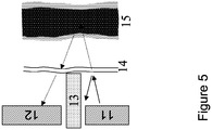
- Light that has not entered the material is of no use for the detector. This is the case when the oxygen content of blood under the skin needs to be measured.
- Light emitted by the LED (11) is partially reflected by the skin (14) and partially transmitted to the blood vessel (15).
- Light coming from the LED (11) or reflected at the skin (14) should not reach the light detector (12) whereas light reflected from the blood (15) should reach the detector (12). Therefore, a light-absorbing or reflecting layer (13) may be included between the LED and detector to prevent the incidence of such undesired light (can be directly incident, or indirectly incident (e.g. after reflection)) into the detector.
- a light absorbing or reflecting structure, element or layer can be present such that the amount of light reaching the detector (originating from the light source, possibly LED) not having penetrated said material is reduced. Therefore the light absorbing or reflecting structure, element or layer can be positioned in the path of direct or indirect illumination of light generated by said emitter towards said detector. An element or layer can put in between the detector and the emitter.
- a light-absorbing layer is obtained by etching a V-groove into the substrate and filling this groove with a material that absorbs light at the wavelength being used.
- the V-groove may be filled with a metal to reflect the undesired light.
- LEDs light detectors and light emitting diodes
- different is meant to indicate that the described elements have different emission or absorption spectra, e.g. they emit or absorb different frequencies. Different wavelengths can easily be obtained when the components, i.e. detectors and LEDs, are made of organic materials. Such components have a different emission and/or absorption spectrum when compared to classical non-organic components.
- the emission and absorption spectrum of organic components can be relatively broad and their absorption spectra may be limited towards higher frequency or energy photons. This means that their emission and absorption spectra can be appropriately chosen for the specific implementation.
- Different combinations of detectors and LEDs are represented below. They can easily be produced in organic materials, but in many cases also in classic non-organic materials. As an example, the measurement of the oxygen content of blood in a tissue is chosen. Different approaches are possible.
- Non-organic LEDs can emit light in a narrow frequency range.
- Non-organic detectors can absorb photons with energy larger then the bandgap energy, which means that if the detector is designed to collect photons of the light of a first, lower, frequency, it would also collect light at a second, higher frequency. This means that emission and detection of light of both frequencies cannot happen at the same time; as only one signal would be generated in the detector.
- Organic light emitting diodes and organic light detectors can cover only a limited frequency range or can cover a wide frequency range.
- Organic detectors optimized for covering both wavelengths are disclosed as well as organic detectors optimized for covering a single wavelength.
- Signals at different wavelengths can be obtained by using a signal generator (e.g., a light generator as for instance a light source), which produces a signal with a broad emission spectrum and at least two signal detectors (e.g. optical detectors) with preferably narrow absorption spectrum.
- a signal generator e.g., a light generator as for instance a light source
- signal detectors e.g. optical detectors
- Organic light emitting diodes and organic light detectors fulfil these requirements.
- a single organic light emitting diode (OLED), two organic light detectors, and a plurality of organic transistors can be combined.
- the OLED can have a wide spectrum, which emits light of a first frequency (e.g., red light) and a second frequency (e.g., different red light or IR light), and for which the emission spectrum is known (see Figure 8 ).
- This figure shows an OLED emission spectrum showing light emission from about 600 nm (yellow) to 800 nm (infrared). Such an approach could be used for weighting the different detected signals as a function of their relative initial strengths.
- a first detector absorbs light in a first frequency range (e.g., the first light frequency), and a second detector absorbs light in a second frequency range (e.g., the second light frequency).
- the first and second frequency range can be substantially centred around the first light frequency and the second light frequency, respectively.
- the detectors can be such that they are mainly absorbing light of the first frequency and the second frequency, respectively. This is illustrated in Figure 7 . It shows the absorption spectra of rather 2 similar molecules, i.e. F16CuPc and NiPc.
- NiPc absorbs substantial more than F16CuPc (about 50% more), whereas at 800 nm F16CuPc absorbs much more than NiPc.
- the frequency ranges preferably do not have a substantial overlap region.
- Oxygen content in the blood gives information on the wound healing process or concerning the location of a bacterial infection.
- a sensor unit can be repeated to cover a larger area, such that parallel measurements over a larger area become possible.
- the sensors units can be repeated in a one- or a two-dimensional array or in other geometrical configurations. The exact location of the sensor units depends on the topography and shape of surface that needs to be measured.
- each sensor unit of the sensor can comprise a single or a plurality of organic light emitting diode and a single or a plurality of organic light detector and circuitry comprising a plurality of organic transistors.
- Blind detectors may be added in some sensor units of such an array to eliminate dark current. These additional light detectors are covered to prevent incident light from entering.
- Each matrix element of a matrix may include two different light emitting diodes, two different light detectors and a plurality of transistors. One of the two detectors may be a blind detector (e.g., can be covered in order to prevent light to fall in).
- Each matrix element of the matrix may include a circuit using the transistors to amplify the signal difference between the two light detectors.
- a blind detector can be used in each matrix cell or in a certain set of matrix cells (for instance a row or a column in a matrix) a blind detector can be used.
- two blind light detectors may be added to each matrix cell or may be added to certain rows or columns of the said matrix.
- Each matrix element of the matrix may include two different light emitting diodes, four different light detectors and a plurality of transistors.
- two of the four said light detectors may be covered to prevent incident light from falling in.
- Two circuits can then be present per matrix cell which use the transistors to amplify the signal difference between a pair two of the light detectors.
- Plastic components may be deposited by e.g. printing, evaporation or spin-coating and other known preferably low-cost techniques for organic electronics fabrication.
- relatively high integration densities can be achieved and different constituting elements can be processed in parallel, i.e. in the same process steps. This also allows for inexpensive production of one and two dimensional arrays with measurement places each having their signal generator and their signal detector and underlying electronics, providing one or two-dimensional pictures of the characteristics of the material under measurement.
- At least one connector for power and signals may be present.
- a pre-amplification circuit may be included within the device.
- a method for reading out the charge on the capacitances of the sensor units includes reading the charges out in a sequential manner to obtain an image of the characteristic.
- Each sensor unit can correspond to one pixel of the image.
- a readout circuit can be integrated in the array of sensor units and may be specifically adapted for use with low-cost organic electronics.
- a display or possibly a flexible display made of organic material may be added to provide the images or measurements.
- the read-out circuitry realises an image of the characteristic on this display.
- Methods that can be used for depositing organic material are printing, evaporation or spin-coating and other known methods.
- Intelligent wound care that allows inspection of wound healing is currently used for different applications.
- An example is the inspection of the "survival of a flap" after an operation in which a part of the skin has been transplanted. Presence of blood flow indicates that the skin will survive.
- Another example is inspection of wound infection by detection of (local) increased blood oxygen consumption. Also detection of bedsores and blood flow problems related to diabetics is possible.
- Different techniques to measure the blood flow through the skin exist, such as duplex US-Doppler echography, IR laser scanning, and NIR reflection spectroscopy. However, the spatial resolution of these techniques is too low. Also opening of the bandage, covering the wound, is required which may impede the healing process. Blood strongly absorbs and scatters red light.
- the blood pressure goes up and down with the heartbeat and so does (by expansion) the volume of blood in the blood vessels.
- the scattering and reflection of all other skin tissue remains unchanged with the heartbeat, only the reflection by the blood vessel changes. This has been used before to determine the heartbeat by the global reflection of a large spot. Also a small spot from a glass fiber has been used to determine the blood flow locally. A physician using such a technique has to move the glass fiber over the wound. Taking such measurements requires that the bandage covering a wound be opened, which increases the risk of infection. Further, the oxygen level can be determined if two different light sources are used, due to the difference in scattering and reflection between oxyhemoglobin and hemoglobin.
- a sensor comprising an array or matrix of different sensor units made of organic materials as described above allows a uniform pressure on a wound. When made in organic materials high spatial resolution can be obtained. Furthermore monitoring blood flow through the skin without opening the bandage is possible.
- Embodiments described above may be integrated in a bandage, which is used to cover and protect wounds. Measuring a characteristic of human or animal tissue or wound of a living human or animal, related to either oxygen or blood flow within the tissue or wound is possible.
- the method includes performing measurements on at least one place on said tissue, or on a plurality of places, preferably arranged in a one or two dimensional array (which may be denoted as matrix or regular grid pattern).
- the measurement duration may exceed at least one heart beat cycle, or a plurality of heat beat cycles, such as for example 10, 50,100, 500, 1,000, 2,000, 5,000, 10,000 or 100,000, heart beat cycles.
- the sets of measurement intervals can correspond with specific repetitions in the heartbeat cycle. In such way, an integrated value and subsequent read-out of said integrated value are achieved and the characteristic of the human or animal tissue can be determined from said integrated value.
- the blood flow in the skin under the bandage can be imaged without opening the bandage.
- the blood oxygen level in the skin under the bandage can also be imaged when active circuitry for measuring two different wavelengths is used. Therefore organic OLEDs with two different wavelengths in combination with 1 broadband organic detector and a plurality of organic transistors may be used. Else OLEDs and corresponding organic detectors of two different colours or frequencies can be used,
- Other characteristics of human or animal tissue which can be measured according to the present invention are for instance linked with the presence or concentration of certain constituents of the blood, or the concentration or presence of markers in the blood, which may have been added to it.
- the presence or concentration has periodic behaviour with a frequency that corresponds to the heartbeat frequency.
- a control logic block which can determine the occurrence of high and low blood pressure is further included.
- Such a control logic block may comprise a plurality of capacitances that are charged by one or more signals originating from one, two or more organic light detector(s) on at about the specific times of high or low blood pressure. Some capacitances may be charged at high blood pressure occurrences while others may be charged at low blood pressure occurrences. These capacitances can be charged over different heartbeat periods as described above, such that the signal-to-noise ratio of the image can be improved.
- the scattered light from the OLEDs is measured by the organic detectors in conjunction with a heartbeat cycle of a patient to which the bandage is applied.
- the difference between high blood-pressure low blood-pressure signals is sampled for several periods to average noise effects out.
- the organic transistors in the circuit control the sampling period, the signal amplification and the read-out selection.
- Embodiments described above may be integrated in a bandage, which is used to cover and protect wounds.
- a matrix of OLEDs, organic detectors and organic transistors can be integrated on a thin foil, preferably a flexible thin foil, that is incorporated into a bandage (see Figure 9 ).
- thin foils may be incorporated in the bandage, each with its own functionality.
- An example is a combination of foils to implement a blood flow patch, an oximeter patch, a direct read-out, a differential read-out with a blind reference detector in the matrix cell, or in a matrix row, or in a matrix column, or one cell per matrix.
- the thin foil(s) on which the OLEDs, organic detectors and organic transistors are disposed may include holes (e.g. round holes, but any shape can be used) or trenches (e.g., rectangular trenches) to allow the wound liquids to be absorbed by other parts of the bandage (e.g., gauze material).
- holes e.g. round holes, but any shape can be used
- trenches e.g., rectangular trenches
- additional layers may be incorporated for wound healing and wound protection.
- a (set of) sealing layer(s) is further included.
- a device in the form of a layer of low-cost plastic electronics is added into a classical disposable bandage that is used to cover a wound, for instance, after an operation or during (emergency) first-aid care.
- This additional layer allows for a read-out to produce an image containing information about the wound healing process. This is done by connecting external contacts on the bandage to appropriate read-out equipment.
- a mechanism for attaching the above-mentioned device removably to the (human) body is included (such as an adhesive strip).
- This measurement method using organic light emitting diodes, organic photo detectors, and organic circuitry may also be included in foils for making colour or grey scale copies of bended surfaces, such as old books.
- a method and tool for copying black and white pictures of bent surfaces is already known.
- Using this method with one organic LED and at least one detector also grey scale copies can be made.
- Using a wideband organic LED and at least three narrow band organic light detectors (for example yellow, blue and red) also colour copies can be made.
- the method may also be used to detect the composition of a gas flowing in a tube. In case this is a periodic flow, the measurement can be done without introducing an extra periodical signal. In case the gas flow is continuous, a periodic signal can be obtained by modulating the organic light emitting diode(s).
Claims (28)
- Ein Sensor, der eine Vielzahl von Sensoreinheiten umfasst, welche in einer ein- oder zweidimensionalen Matrix angeordnet sind, wobei jede Sensoreinheit Folgendes umfasst:• ein Ladungsspeicherelement,• ein erstes Messelement, um bei ersten Malen einen ersten Messstrom zu erzeugen, welcher erwünschte Komponenten und unerwünschte Komponenten A und B umfasst, und bei zweiten Malen einen dritten Messstrom, welcher aus den unerwünschten Komponenten A und B besteht;• ein zweites Messelement, um bei den erwähnten ersten und zweiten Malen respektive einen zweiten Messstrom und einen vierten Messstrom zu erzeugen, die jeweils die unerwünschte Komponente A umfassen,• ein erstes Schaltkreisteil verbunden zwischen dem erwähnten Ladungsspeicherelement und dem erwähnten ersten und zweiten Messelement, wobei das erwähnte erste Schaltkreisteil konfiguriert ist, um periodisch einen Ladestrom auf das erwähnte Ladungsspeicherelement anzuwenden, um das erwähnte Ladungsspeicherelement über eine vorbestimmte Anzahl von Perioden zu laden, wobei der erwähnte Ladestrom der erste Messstrom abzüglich des zweiten Messstroms ist, wobei das erwähnte erste Schaltkreisteil erste Umschaltelemente umfasst,• ein zweites Schaltkreisteil verbunden zwischen dem erwähnten Ladungsspeicherelement und dem erwähnten ersten und zweiten Messelement, wobei das erwähnte zweite Schaltkreisteil konfiguriert ist, um periodisch einen Entladestrom auf das Ladungsspeicherelement anzuwenden, um das erwähnte Ladungsspeicherelement über eine vorbestimmte Anzahl von Perioden zu entladen, wobei der erwähnte Entladestrom der dritte Messstrom abzüglich des vierten Messstroms ist, wobei das erwähnte zweite Schaltkreisteil zweite Umschaltelemente umfasst,• wobei die ersten und zweiten Umschaltelemente zwischen einem leitenden Zustand und einem nicht-leitenden Zustand umschaltbar sind,• ein drittes Schaltkreisteil verbunden zwischen dem erwähnten Ladungsspeicherelement und einem Ausgang des erwähnten Sensors, wobei das erwähnte dritte Schaltkreisteil ein drittes Umschaltelement umfasst, umschaltbar zwischen einem leitenden und einem nicht-leitenden Zustand, wobei das dritte Umschaltelement angeordnet ist, um auf dem Ladungsspeicherelement gespeicherte Ladung zum erwähnten Ausgang zu leiten, wobei das dritte Schaltkreisteil konzipiert ist, um die erwähnte Ladung nach der erwähnten vorbestimmten Anzahl von Perioden periodisch zu leiten,• Kontrollkreislauf zur Anwendung von Spannungen auf die erwähnten ersten und zweiten Umschaltelemente gemäß eines voreingestellten periodischen Zeitschemas, sodass in jeder Periode des erwähnten Zeitschemas die erwähnten ersten und zweiten Umschaltelemente für eine bestimmte Zeit auf den leitenden Zustand umgeschaltet werden und sodass die unerwünschten Komponenten A und B aufgrund der ladenden und entladenden Ströme aus der auf dem erwähnten Ladungsspeicherelement gespeicherten Ladung entfernt werden.
- Ein Sensor nach Anspruch 1, dadurch gekennzeichnet, dass das erwähnte erste Schaltkreisteil aus den erwähnten ersten Umschaltelementen besteht, dass das erwähnte zweite Schaltkreisteil aus den erwähnten zweiten Umschaltelementen und einem Stromspiegel besteht und dass das dritte Schaltkreisteil aus dem erwähnten dritten Umschaltelement besteht.
- Ein Sensor nach Ansprüchen 1 oder 2, wobei jede Sensoreinheit angepasst ist, um ein periodisches Messsignal zu verarbeiten, und wobei das erwähnte Zeitschema so bestimmt ist, dass der erwähnte Ladestrom rund um den Höchstwert des erwähnten periodischen Messsignals liegt und der erwähnte Entladestrom rund um den Mindestwert des erwähnten periodischen Messsignals liegt.
- Ein Verfahren nach Anspruch 3, wobei der erwähnte Kontrollschaltkreis einen Steuerungslogikblock umfasst, um das Auftreten des erwähnten Höchstwertes und des erwähnten Mindestwertes zu bestimmen.
- Ein Sensor nach Ansprüchen 1 oder 2 oder 3, wobei für jede Sensoreinheit das erwähnte erste Messelement zumindest einen Lichtdetektor verbunden mit dem erwähnten ersten und zweiten Schaltkreisteil umfasst und wobei das erwähnte Zeitschema mit einem periodischen Beleuchtungsschema des erwähnten zumindest einen Lichtdetektors synchronisiert ist.
- Ein Sensor nach Anspruch 5, wobei das erwähnte zweite Messelement einen blinden Detektor umfasst, verbunden mit dem erwähnten ersten und zweiten Schaltkreisteil, wobei der erwähnte blinde Detektor ein von einfallendem Licht abgeschirmter Lichtdetektor ist.
- Ein Sensor nach Anspruch 5 oder 6, wobei jede Sensoreinheit ferner zumindest eine Leuchtdiode umfasst.
- Ein Sensor nach Anspruch 7, wobei jede Sensoreinheit ferner eine Licht absorbierende oder Licht reflektierende Schicht zwischen der erwähnten zumindest einen Leuchtdiode und dem erwähnten zumindest einen Lichtdetektor umfasst.
- Ein Sensor nach Ansprüchen 7 oder 8, wobei jede Sensoreinheit eine Leuchtdiode mit einem breiten Emissionsspektrum, zwei Lichtdetektoren mit einem schmalen Absorptionsspektrum umfasst, wobei die erwähnten schmalen Absorptionsspektren der erwähnten zwei Lichtdetektoren unterschiedlich sind, wobei die erwähnten zwei schmalen Absorptionsspektren in das erwähnte breite Emissionsspektrum der erwähnten Leuchtdiode fallen.
- Ein Sensor nach irgendeinem der vorigen Ansprüche, welcher ferner zumindest einen Konnektor für Energie und Signale umfasst.
- Ein Sensor nach irgendeinem der vorigen Ansprüche, welcher ferner Ausleseelektronik zum sequenziellen Auslesen der erwähnten Sensoreinheiten umfasst.
- Ein Sensor nach Anspruch 11, welcher ferner eine Anzeige umfasst, wobei die erwähnte Ausleseelektronik bereitgestellt ist, um auf der erwähnten Anzeige ein ein- oder zweidimensionales Bild der erwähnten Ladungen auf den erwähnten Ladungsspeicherelementen in einer erwähnten ein- oder zweidimensionalen Matrix zu erstellen.
- Ein Sensor nach irgendeinem der Ansprüche 7 bis 9, wobei die erwähnte Leuchtdiode, die erwähnten Schaltkreisteile, das erwähnte Ladungsspeicherelement und die erwähnten Detektoren aus organischen Materialien hergestellt sind.
- Ein Sensor nach Anspruch 13, der ferner ein flexibles Material umfasst.
- Ein Sensor nach Anspruch 14, wobei das erwähnte flexible Material ein Verband zum Abdecken einer Wunde ist.
- Ein Sensor nach Anspruch 14, wobei das erwähnte flexible Material eine in einen Verband zum Abdecken einer Wunde integrierte Folie ist.
- Ein Sensor nach Anspruch 16, wobei die erwähnte Folie eine erste Folie umfasst, welche die erwähnten organischen Leuchtdioden umfasst, eine zweite Folie, welche die erwähnten organischen Lichtdetektoren umfasst, und eine dritte Folie, welche jedes der erwähnten Schaltkreisteile umfasst.
- Ein Sensor nach Anspruch 17, wobei die erwähnten Folien Löcher oder Rinnen enthalten.
- Ein Verfahren zum Entfernen einer oder mehrerer unerwünschter Komponenten aus einem Messsignal in Verbindung mit einem Merkmal, wobei ein Sensor nach Anspruch 1 verwendet wird, wobei das erwähnte Verfahren die folgenden Schritte in jeder Sensoreinheit umfasst:a) Messen bei ersten Malen eines ersten Messwertes des erwähnten Messsignals mittels des ersten und zweiten Messelements, wobei das erste Messelement den ersten Messstrom erzeugt, welcher erwünschte Komponenten und unerwünschte Komponenten A und B umfasst, und das zweite Messelement den zweiten Messstrom erzeugt, welcher die unerwünschte Komponente A umfasst,b) Anwenden des Ladestroms, welcher der erste Messstrom abzüglich des zweiten Messstroms ist, auf das Ladungsspeicherelement der jeweiligen Sensoreinheit während einer bestimmten Zeit zum Laden mittels der ersten Umschaltelemente der jeweiligen Sensoreinheit,c) Messen bei zweiten Malen eines zweiten Messwertes des erwähnten Messsignals mittels des ersten und zweiten Messelements, wobei das erste Messelement den dritten Messstrom erzeugt, welcher aus den unerwünschten Komponenten A und B besteht, und das zweite Messelement den vierten Messstrom erzeugt, welcher die unerwünschte Komponente A umfasst,d) Anwenden des Entladestroms, welcher der dritte Messstrom abzüglich des vierten Messstroms ist, auf das erwähnte Ladungsspeicherelement während einer bestimmten Zeit zum Entladen mittels der zweiten Umschaltelemente der jeweiligen Sensoreinheit, sodass die unerwünschten Komponenten A und B mittels der Lade- und Entladeströme aus der auf dem erwähnten Ladungsspeicherelement gespeicherten Ladung entfernt werden,e) eine vorbestimmen Anzahl von Malen Wiederholen der Schritte a) bis d),f) Leiten von auf dem erwähnten Ladungsspeicherelement akkumulierter Ladung zu einem Ausgang mittels des dritten Umschaltelements der jeweiligen Sensoreinheit.
- Ein Verfahren nach Anspruch 19, wobei das erwähnte Messsignal ein periodisches Signal ist.
- Ein Verfahren nach Anspruch 20, wobei die erwähnten ersten Male rund um den Höchstwert des erwähnten periodischen Signals gewählt werden und die erwähnten zweiten Male rund um den Mindestwert des erwähnten periodischen Signals gewählt werden.
- Ein Verfahren nach Ansprüchen 19 oder 20 oder 21, wobei das erste und zweite Messelement Lichtdetektoren sind.
- Ein Verfahren nach Anspruch 22, wobei der erwähnte zweite Lichtdetektor ein blinder Detektor ist, wobei der erwähnte blinde Detektor ein von einfallendem Licht abgeschirmter Lichtdetektor ist.
- Ein Verfahren nach irgendeinem der Ansprüche 19 bis 23, welches ferner den Schritt des Beleuchtens jedes Lichtdetektors mittels zumindest einer Leuchtdiode umfasst.
- Ein Verfahren nach Anspruch 24, wobei die erwähnte zumindest eine Leuchtdiode eine Leuchtdiode mit einem breiten Emissionsspektrum umfasst, wobei der erste Lichtdetektor ein erstes schmales Absorptionsspektrum hat, und wobei der zweite Lichtdetektor ein zweites schmales Absorptionsspektrum hat, wobei das erwähnte erste und zweite schmale Absorptionsspektrum des erwähnten ersten und zweiten Lichtdetektors unterschiedlich sind, wobei das erwähnte erste und zweite schmale Absorptionsspektrum innerhalb des erwähnten breiten Emissionsspektrums der erwähnten Leuchtdiode liegen.
- Ein Verfahren nach irgendeinem der Ansprüche 19 bis 25, welches ferner Folgendes umfasst:g) Ausführen von a) bis e) an einer Vielzahl von Stellen in der ein- oder zweidimensionalen Matrix,h) sequenzielles Leiten der erwähnten Ladungen, die auf den erwähnten Ladungsspeicherelementen gespeichert sind, an der erwähnten Vielzahl von Stellen zum erwähnten Ausgang.i) Anzeigen der erwähnten Ladungen auf den erwähnten Ladungsspeicherelementen als ein ein- oder zweidimensionales Bild.
- Ein Verfahren nach irgendeinem der Ansprüche 19 bis 26, wobei das erwähnte Merkmal aus der Gruppe bestehend aus Blutstrom, Sauerstoffgehalt im Blut, Blutbestandteilen, Anwesenheit von Markern im Blut, und Konzentration von Markern im Blut ausgewählt wird.
- Ein Verfahren nach Anspruch 27, wobei das erwähnte Messsignal der Herzschlagzyklus ist und wobei der erwähnte erste Messwert rund um den höchsten Blutdruck erfasst wird und der erwähnte zweite Messwert rund um den niedrigsten Blutdruck erfasst wird.
Applications Claiming Priority (2)
| Application Number | Priority Date | Filing Date | Title |
|---|---|---|---|
| US67256805P | 2005-04-18 | 2005-04-18 | |
| PCT/EP2006/061343 WO2006111472A2 (en) | 2005-04-18 | 2006-04-05 | Sensor for eliminating undesired components and measurement method using said sensor |
Publications (2)
| Publication Number | Publication Date |
|---|---|
| EP1872101A2 EP1872101A2 (de) | 2008-01-02 |
| EP1872101B1 true EP1872101B1 (de) | 2017-10-18 |
Family
ID=36928639
Family Applications (1)
| Application Number | Title | Priority Date | Filing Date |
|---|---|---|---|
| EP06725573.7A Not-in-force EP1872101B1 (de) | 2005-04-18 | 2006-04-05 | Sensor zur beseitigung unerwünschter komponenten und den sensor verwendendes messverfahren |
Country Status (3)
| Country | Link |
|---|---|
| US (1) | US8423105B2 (de) |
| EP (1) | EP1872101B1 (de) |
| WO (1) | WO2006111472A2 (de) |
Families Citing this family (15)
| Publication number | Priority date | Publication date | Assignee | Title |
|---|---|---|---|---|
| GB0607270D0 (en) * | 2006-04-11 | 2006-05-17 | Univ Nottingham | The pulsing blood supply |
| CN101466304B (zh) * | 2006-06-12 | 2011-11-09 | 皇家飞利浦电子股份有限公司 | 皮肤监测设备、监测皮肤的方法、监测设备、照射皮肤的方法以及oled的用途 |
| JP5261379B2 (ja) * | 2006-06-12 | 2013-08-14 | コーニンクレッカ フィリップス エレクトロニクス エヌ ヴィ | 人体監視装置、人体データ取得方法、並びに、傷の存在、場所、及び/又は、段階に関するデータを取得する方法 |
| US8251903B2 (en) * | 2007-10-25 | 2012-08-28 | Valencell, Inc. | Noninvasive physiological analysis using excitation-sensor modules and related devices and methods |
| US11944432B1 (en) * | 2008-12-02 | 2024-04-02 | Vioptix, Inc. | Flexible oximeter sensor panel |
| US8452366B2 (en) | 2009-03-16 | 2013-05-28 | Covidien Lp | Medical monitoring device with flexible circuitry |
| US8384443B2 (en) * | 2011-01-27 | 2013-02-26 | Maxim Integrated Products, Inc. | Current mirror and current cancellation circuit |
| WO2013019494A2 (en) | 2011-08-02 | 2013-02-07 | Valencell, Inc. | Systems and methods for variable filter adjustment by heart rate metric feedback |
| US9649055B2 (en) * | 2012-03-30 | 2017-05-16 | General Electric Company | System and methods for physiological monitoring |
| DK177485B1 (en) * | 2012-10-05 | 2013-07-15 | Designit As | DEVICE FOR PEOPLE WITH DISABLED SENSE OR DISABLED PEOPLE |
| US10945618B2 (en) | 2015-10-23 | 2021-03-16 | Valencell, Inc. | Physiological monitoring devices and methods for noise reduction in physiological signals based on subject activity type |
| WO2017070463A1 (en) | 2015-10-23 | 2017-04-27 | Valencell, Inc. | Physiological monitoring devices and methods that identify subject activity type |
| US10966662B2 (en) | 2016-07-08 | 2021-04-06 | Valencell, Inc. | Motion-dependent averaging for physiological metric estimating systems and methods |
| US20180113022A1 (en) * | 2016-10-20 | 2018-04-26 | Osram Opto Semiconductors Gmbh | Integrated circuit for sensor applications |
| EP4096512A4 (de) | 2021-04-11 | 2023-11-01 | Alio, Inc. | Systeme und verfahren zur messung biologischer metriken und blutgefässgeometrie mit einer fotoplethysmographievorrichtung mit mehreren optischen pfaden |
Family Cites Families (15)
| Publication number | Priority date | Publication date | Assignee | Title |
|---|---|---|---|---|
| GB2126776B (en) * | 1982-08-26 | 1985-12-04 | British Aerospace | Ring laser gyroscopes |
| DE3620931A1 (de) * | 1986-06-23 | 1988-01-07 | Siemens Ag | Empfaenger fuer optische digitalsignale |
| US6549795B1 (en) * | 1991-05-16 | 2003-04-15 | Non-Invasive Technology, Inc. | Spectrophotometer for tissue examination |
| US5488415A (en) * | 1993-07-09 | 1996-01-30 | Olympus Optical Co., Ltd. | Solid-state image pickup device having a photoelectric conversion detection cell with high sensitivity |
| US5705807A (en) * | 1994-10-24 | 1998-01-06 | Nissan Motor Co., Ltd. | Photo detecting apparatus for detecting reflected light from an object and excluding an external light componet from the reflected light |
| US5912463A (en) * | 1996-08-19 | 1999-06-15 | Hamamatsu Photonics K.K. | Photodetector and solid-state imaging apparatus |
| US5817008A (en) * | 1996-10-31 | 1998-10-06 | Spacelabs Medical, Inc. | Conformal pulse oximetry sensor and monitor |
| EP1118208B1 (de) * | 1998-09-28 | 2004-11-10 | 3DV Systems Ltd. | Entfernungsmessung mittels kamera |
| US6519486B1 (en) * | 1998-10-15 | 2003-02-11 | Ntc Technology Inc. | Method, apparatus and system for removing motion artifacts from measurements of bodily parameters |
| US6505060B1 (en) | 2000-09-29 | 2003-01-07 | Datex-Ohmeda, Inc. | Method and apparatus for determining pulse oximetry differential values |
| GB2377489A (en) * | 2001-06-22 | 2003-01-15 | Martin Ferguson-Pell | Optoelectronic device for characterising tissue perfusion in dermis |
| JP3918635B2 (ja) * | 2002-05-30 | 2007-05-23 | ソニー株式会社 | 直流レベル制御方法、クランプ回路、撮像装置 |
| US6876233B1 (en) * | 2003-02-15 | 2005-04-05 | Medtronics, Inc. | DC cancellation apparatus and method |
| JP2006523074A (ja) * | 2003-04-11 | 2006-10-05 | カネスタ インコーポレイテッド | センサのダイナミックレンジを差分拡大する方法及びシステム |
| EP1475957B1 (de) | 2003-05-08 | 2010-11-03 | STMicroelectronics (Research & Development) Limited | Verfahren und Vorrichtung zur Entfernung von Spaltenfestmusterrauschen in Festkörperbildsensoren |
-
2006
- 2006-04-05 US US11/918,816 patent/US8423105B2/en not_active Expired - Fee Related
- 2006-04-05 WO PCT/EP2006/061343 patent/WO2006111472A2/en active Application Filing
- 2006-04-05 EP EP06725573.7A patent/EP1872101B1/de not_active Not-in-force
Non-Patent Citations (1)
| Title |
|---|
| None * |
Also Published As
| Publication number | Publication date |
|---|---|
| US8423105B2 (en) | 2013-04-16 |
| EP1872101A2 (de) | 2008-01-02 |
| WO2006111472A3 (en) | 2007-04-05 |
| US20080312517A1 (en) | 2008-12-18 |
| WO2006111472A2 (en) | 2006-10-26 |
| WO2006111472A8 (en) | 2007-12-13 |
Similar Documents
| Publication | Publication Date | Title |
|---|---|---|
| EP1872101B1 (de) | Sensor zur beseitigung unerwünschter komponenten und den sensor verwendendes messverfahren | |
| JP5143471B2 (ja) | イメージング装置 | |
| US10841504B1 (en) | Fluorescence imaging with minimal area monolithic image sensor | |
| US5833603A (en) | Implantable biosensing transponder | |
| US7248906B2 (en) | Method and device for monitoring analyte concentration by optical detection | |
| US20180125407A1 (en) | Transcutaneous organ function measurement | |
| US20020103417A1 (en) | Endoscopic smart probe and method | |
| JP4327738B2 (ja) | 生体光計測装置及び生体光計測方法 | |
| JP5623540B2 (ja) | 生体情報取得解析装置 | |
| US11633089B2 (en) | Fluorescence imaging with minimal area monolithic image sensor | |
| CN108780044A (zh) | 用于寿命成像和检测应用的传感器和设备 | |
| CN107468209A (zh) | 摄像装置 | |
| US20170303838A1 (en) | Analyte-sensing device | |
| KR102649561B1 (ko) | 유기 광 감지소자 기반의 비침습형 생체 센서 | |
| US11187658B2 (en) | Fluorescence imaging with fixed pattern noise cancellation | |
| US20200404202A1 (en) | Fluorescence imaging with fixed pattern noise cancellation | |
| US20200404201A1 (en) | Fluorescence imaging with fixed pattern noise cancellation | |
| CN114144115A (zh) | 内窥镜超光谱成像系统中的图像旋转 | |
| US20200404140A1 (en) | Fluorescence imaging with minimal area monolithic image sensor | |
| CN114206196A (zh) | 控制荧光成像系统中的激光脉冲的积分能量 | |
| JP4332628B2 (ja) | 生体組織測定用イメージセンサ及び該センサを用いた生体組織測定方法 | |
| JP2019136498A (ja) | 心拍センサ、心拍センサが組み込まれた近赤外線有機イメージセンサ及びこれを含むスマートフォン、並びにウェアラブル心拍センサ、血管造影装置 | |
| US10835126B1 (en) | Implantable micro-spectrophotometer | |
| Ng et al. | A Complementary Metal–Oxide–Semiconductor Image Sensor for On-Chip in Vitro and in Vivo Imaging of the Mouse Hippocampus | |
| Chiarelli et al. | Wearable, fiber-less, multi-channel system for continuous wave functional near infrared spectroscopy based on silicon photomultipliers detectors and lock-in amplification |
Legal Events
| Date | Code | Title | Description |
|---|---|---|---|
| PUAI | Public reference made under article 153(3) epc to a published international application that has entered the european phase |
Free format text: ORIGINAL CODE: 0009012 |
|
| 17P | Request for examination filed |
Effective date: 20071015 |
|
| AK | Designated contracting states |
Kind code of ref document: A2 Designated state(s): AT BE BG CH CY CZ DE DK EE ES FI FR GB GR HU IE IS IT LI LT LU LV MC NL PL PT RO SE SI SK TR |
|
| R17D | Deferred search report published (corrected) |
Effective date: 20071213 |
|
| DAX | Request for extension of the european patent (deleted) | ||
| 17Q | First examination report despatched |
Effective date: 20080718 |
|
| RAP1 | Party data changed (applicant data changed or rights of an application transferred) |
Owner name: IMEC |
|
| GRAP | Despatch of communication of intention to grant a patent |
Free format text: ORIGINAL CODE: EPIDOSNIGR1 |
|
| STAA | Information on the status of an ep patent application or granted ep patent |
Free format text: STATUS: GRANT OF PATENT IS INTENDED |
|
| RIC1 | Information provided on ipc code assigned before grant |
Ipc: A61B 5/00 20060101AFI20161114BHEP Ipc: G01J 1/46 20060101ALI20161114BHEP Ipc: H01L 31/02 20060101ALN20161114BHEP Ipc: H01L 51/00 20060101ALN20161114BHEP Ipc: H01L 31/12 20060101ALI20161114BHEP Ipc: H01L 27/146 20060101ALI20161114BHEP Ipc: H01L 27/30 20060101ALN20161114BHEP Ipc: A61B 5/1455 20060101ALI20161114BHEP |
|
| INTG | Intention to grant announced |
Effective date: 20161213 |
|
| GRAS | Grant fee paid |
Free format text: ORIGINAL CODE: EPIDOSNIGR3 |
|
| GRAJ | Information related to disapproval of communication of intention to grant by the applicant or resumption of examination proceedings by the epo deleted |
Free format text: ORIGINAL CODE: EPIDOSDIGR1 |
|
| GRAL | Information related to payment of fee for publishing/printing deleted |
Free format text: ORIGINAL CODE: EPIDOSDIGR3 |
|
| STAA | Information on the status of an ep patent application or granted ep patent |
Free format text: STATUS: EXAMINATION IS IN PROGRESS |
|
| REG | Reference to a national code |
Ref country code: DE Ref legal event code: R079 Ref document number: 602006053878 Country of ref document: DE Free format text: PREVIOUS MAIN CLASS: G01J0001420000 Ipc: A61B0005000000 |
|
| GRAP | Despatch of communication of intention to grant a patent |
Free format text: ORIGINAL CODE: EPIDOSNIGR1 |
|
| STAA | Information on the status of an ep patent application or granted ep patent |
Free format text: STATUS: GRANT OF PATENT IS INTENDED |
|
| INTC | Intention to grant announced (deleted) | ||
| RIC1 | Information provided on ipc code assigned before grant |
Ipc: G01J 1/46 20060101ALI20170301BHEP Ipc: A61B 5/1455 20060101ALI20170301BHEP Ipc: H01L 51/00 20060101ALN20170301BHEP Ipc: H01L 27/30 20060101ALN20170301BHEP Ipc: H01L 27/146 20060101ALI20170301BHEP Ipc: H01L 31/12 20060101ALI20170301BHEP Ipc: H01L 31/02 20060101ALN20170301BHEP Ipc: A61B 5/00 20060101AFI20170301BHEP |
|
| INTG | Intention to grant announced |
Effective date: 20170320 |
|
| GRAA | (expected) grant |
Free format text: ORIGINAL CODE: 0009210 |
|
| STAA | Information on the status of an ep patent application or granted ep patent |
Free format text: STATUS: THE PATENT HAS BEEN GRANTED |
|
| AK | Designated contracting states |
Kind code of ref document: B1 Designated state(s): AT BE BG CH CY CZ DE DK EE ES FI FR GB GR HU IE IS IT LI LT LU LV MC NL PL PT RO SE SI SK TR |
|
| REG | Reference to a national code |
Ref country code: GB Ref legal event code: FG4D |
|
| REG | Reference to a national code |
Ref country code: CH Ref legal event code: EP |
|
| REG | Reference to a national code |
Ref country code: AT Ref legal event code: REF Ref document number: 937224 Country of ref document: AT Kind code of ref document: T Effective date: 20171115 Ref country code: IE Ref legal event code: FG4D |
|
| REG | Reference to a national code |
Ref country code: DE Ref legal event code: R096 Ref document number: 602006053878 Country of ref document: DE |
|
| RAP2 | Party data changed (patent owner data changed or rights of a patent transferred) |
Owner name: IMEC VZW |
|
| REG | Reference to a national code |
Ref country code: NL Ref legal event code: MP Effective date: 20171018 |
|
| REG | Reference to a national code |
Ref country code: LT Ref legal event code: MG4D |
|
| REG | Reference to a national code |
Ref country code: AT Ref legal event code: MK05 Ref document number: 937224 Country of ref document: AT Kind code of ref document: T Effective date: 20171018 |
|
| REG | Reference to a national code |
Ref country code: FR Ref legal event code: PLFP Year of fee payment: 13 |
|
| PG25 | Lapsed in a contracting state [announced via postgrant information from national office to epo] |
Ref country code: NL Free format text: LAPSE BECAUSE OF FAILURE TO SUBMIT A TRANSLATION OF THE DESCRIPTION OR TO PAY THE FEE WITHIN THE PRESCRIBED TIME-LIMIT Effective date: 20171018 |
|
| PG25 | Lapsed in a contracting state [announced via postgrant information from national office to epo] |
Ref country code: LT Free format text: LAPSE BECAUSE OF FAILURE TO SUBMIT A TRANSLATION OF THE DESCRIPTION OR TO PAY THE FEE WITHIN THE PRESCRIBED TIME-LIMIT Effective date: 20171018 Ref country code: ES Free format text: LAPSE BECAUSE OF FAILURE TO SUBMIT A TRANSLATION OF THE DESCRIPTION OR TO PAY THE FEE WITHIN THE PRESCRIBED TIME-LIMIT Effective date: 20171018 Ref country code: SE Free format text: LAPSE BECAUSE OF FAILURE TO SUBMIT A TRANSLATION OF THE DESCRIPTION OR TO PAY THE FEE WITHIN THE PRESCRIBED TIME-LIMIT Effective date: 20171018 Ref country code: FI Free format text: LAPSE BECAUSE OF FAILURE TO SUBMIT A TRANSLATION OF THE DESCRIPTION OR TO PAY THE FEE WITHIN THE PRESCRIBED TIME-LIMIT Effective date: 20171018 |
|
| PG25 | Lapsed in a contracting state [announced via postgrant information from national office to epo] |
Ref country code: IS Free format text: LAPSE BECAUSE OF FAILURE TO SUBMIT A TRANSLATION OF THE DESCRIPTION OR TO PAY THE FEE WITHIN THE PRESCRIBED TIME-LIMIT Effective date: 20180218 Ref country code: LV Free format text: LAPSE BECAUSE OF FAILURE TO SUBMIT A TRANSLATION OF THE DESCRIPTION OR TO PAY THE FEE WITHIN THE PRESCRIBED TIME-LIMIT Effective date: 20171018 Ref country code: BG Free format text: LAPSE BECAUSE OF FAILURE TO SUBMIT A TRANSLATION OF THE DESCRIPTION OR TO PAY THE FEE WITHIN THE PRESCRIBED TIME-LIMIT Effective date: 20180118 Ref country code: GR Free format text: LAPSE BECAUSE OF FAILURE TO SUBMIT A TRANSLATION OF THE DESCRIPTION OR TO PAY THE FEE WITHIN THE PRESCRIBED TIME-LIMIT Effective date: 20180119 Ref country code: AT Free format text: LAPSE BECAUSE OF FAILURE TO SUBMIT A TRANSLATION OF THE DESCRIPTION OR TO PAY THE FEE WITHIN THE PRESCRIBED TIME-LIMIT Effective date: 20171018 |
|
| REG | Reference to a national code |
Ref country code: DE Ref legal event code: R097 Ref document number: 602006053878 Country of ref document: DE |
|
| PG25 | Lapsed in a contracting state [announced via postgrant information from national office to epo] |
Ref country code: CZ Free format text: LAPSE BECAUSE OF FAILURE TO SUBMIT A TRANSLATION OF THE DESCRIPTION OR TO PAY THE FEE WITHIN THE PRESCRIBED TIME-LIMIT Effective date: 20171018 Ref country code: SK Free format text: LAPSE BECAUSE OF FAILURE TO SUBMIT A TRANSLATION OF THE DESCRIPTION OR TO PAY THE FEE WITHIN THE PRESCRIBED TIME-LIMIT Effective date: 20171018 Ref country code: EE Free format text: LAPSE BECAUSE OF FAILURE TO SUBMIT A TRANSLATION OF THE DESCRIPTION OR TO PAY THE FEE WITHIN THE PRESCRIBED TIME-LIMIT Effective date: 20171018 Ref country code: DK Free format text: LAPSE BECAUSE OF FAILURE TO SUBMIT A TRANSLATION OF THE DESCRIPTION OR TO PAY THE FEE WITHIN THE PRESCRIBED TIME-LIMIT Effective date: 20171018 |
|
| PLBE | No opposition filed within time limit |
Free format text: ORIGINAL CODE: 0009261 |
|
| STAA | Information on the status of an ep patent application or granted ep patent |
Free format text: STATUS: NO OPPOSITION FILED WITHIN TIME LIMIT |
|
| PG25 | Lapsed in a contracting state [announced via postgrant information from national office to epo] |
Ref country code: PL Free format text: LAPSE BECAUSE OF FAILURE TO SUBMIT A TRANSLATION OF THE DESCRIPTION OR TO PAY THE FEE WITHIN THE PRESCRIBED TIME-LIMIT Effective date: 20171018 Ref country code: RO Free format text: LAPSE BECAUSE OF FAILURE TO SUBMIT A TRANSLATION OF THE DESCRIPTION OR TO PAY THE FEE WITHIN THE PRESCRIBED TIME-LIMIT Effective date: 20171018 Ref country code: IT Free format text: LAPSE BECAUSE OF FAILURE TO SUBMIT A TRANSLATION OF THE DESCRIPTION OR TO PAY THE FEE WITHIN THE PRESCRIBED TIME-LIMIT Effective date: 20171018 |
|
| 26N | No opposition filed |
Effective date: 20180719 |
|
| PG25 | Lapsed in a contracting state [announced via postgrant information from national office to epo] |
Ref country code: SI Free format text: LAPSE BECAUSE OF FAILURE TO SUBMIT A TRANSLATION OF THE DESCRIPTION OR TO PAY THE FEE WITHIN THE PRESCRIBED TIME-LIMIT Effective date: 20171018 Ref country code: MC Free format text: LAPSE BECAUSE OF FAILURE TO SUBMIT A TRANSLATION OF THE DESCRIPTION OR TO PAY THE FEE WITHIN THE PRESCRIBED TIME-LIMIT Effective date: 20171018 |
|
| REG | Reference to a national code |
Ref country code: CH Ref legal event code: PL |
|
| REG | Reference to a national code |
Ref country code: BE Ref legal event code: MM Effective date: 20180430 |
|
| REG | Reference to a national code |
Ref country code: IE Ref legal event code: MM4A |
|
| PG25 | Lapsed in a contracting state [announced via postgrant information from national office to epo] |
Ref country code: LU Free format text: LAPSE BECAUSE OF NON-PAYMENT OF DUE FEES Effective date: 20180405 |
|
| PG25 | Lapsed in a contracting state [announced via postgrant information from national office to epo] |
Ref country code: CH Free format text: LAPSE BECAUSE OF NON-PAYMENT OF DUE FEES Effective date: 20180430 Ref country code: LI Free format text: LAPSE BECAUSE OF NON-PAYMENT OF DUE FEES Effective date: 20180430 Ref country code: BE Free format text: LAPSE BECAUSE OF NON-PAYMENT OF DUE FEES Effective date: 20180430 |
|
| PG25 | Lapsed in a contracting state [announced via postgrant information from national office to epo] |
Ref country code: IE Free format text: LAPSE BECAUSE OF NON-PAYMENT OF DUE FEES Effective date: 20180405 |
|
| PG25 | Lapsed in a contracting state [announced via postgrant information from national office to epo] |
Ref country code: TR Free format text: LAPSE BECAUSE OF FAILURE TO SUBMIT A TRANSLATION OF THE DESCRIPTION OR TO PAY THE FEE WITHIN THE PRESCRIBED TIME-LIMIT Effective date: 20171018 |
|
| PGFP | Annual fee paid to national office [announced via postgrant information from national office to epo] |
Ref country code: GB Payment date: 20200323 Year of fee payment: 15 |
|
| PG25 | Lapsed in a contracting state [announced via postgrant information from national office to epo] |
Ref country code: PT Free format text: LAPSE BECAUSE OF FAILURE TO SUBMIT A TRANSLATION OF THE DESCRIPTION OR TO PAY THE FEE WITHIN THE PRESCRIBED TIME-LIMIT Effective date: 20171018 Ref country code: HU Free format text: LAPSE BECAUSE OF FAILURE TO SUBMIT A TRANSLATION OF THE DESCRIPTION OR TO PAY THE FEE WITHIN THE PRESCRIBED TIME-LIMIT; INVALID AB INITIO Effective date: 20060405 |
|
| PG25 | Lapsed in a contracting state [announced via postgrant information from national office to epo] |
Ref country code: CY Free format text: LAPSE BECAUSE OF FAILURE TO SUBMIT A TRANSLATION OF THE DESCRIPTION OR TO PAY THE FEE WITHIN THE PRESCRIBED TIME-LIMIT Effective date: 20171018 |
|
| PGFP | Annual fee paid to national office [announced via postgrant information from national office to epo] |
Ref country code: FR Payment date: 20200319 Year of fee payment: 15 |
|
| PGFP | Annual fee paid to national office [announced via postgrant information from national office to epo] |
Ref country code: DE Payment date: 20200319 Year of fee payment: 15 |
|
| REG | Reference to a national code |
Ref country code: DE Ref legal event code: R119 Ref document number: 602006053878 Country of ref document: DE |
|
| GBPC | Gb: european patent ceased through non-payment of renewal fee |
Effective date: 20210405 |
|
| PG25 | Lapsed in a contracting state [announced via postgrant information from national office to epo] |
Ref country code: FR Free format text: LAPSE BECAUSE OF NON-PAYMENT OF DUE FEES Effective date: 20210430 Ref country code: GB Free format text: LAPSE BECAUSE OF NON-PAYMENT OF DUE FEES Effective date: 20210405 Ref country code: DE Free format text: LAPSE BECAUSE OF NON-PAYMENT OF DUE FEES Effective date: 20211103 |