EP1870691A2 - Planar View Sample Preparation - Google Patents
Planar View Sample Preparation Download PDFInfo
- Publication number
- EP1870691A2 EP1870691A2 EP07110824A EP07110824A EP1870691A2 EP 1870691 A2 EP1870691 A2 EP 1870691A2 EP 07110824 A EP07110824 A EP 07110824A EP 07110824 A EP07110824 A EP 07110824A EP 1870691 A2 EP1870691 A2 EP 1870691A2
- Authority
- EP
- European Patent Office
- Prior art keywords
- sample
- probe
- angle
- shaft
- degrees
- Prior art date
- Legal status (The legal status is an assumption and is not a legal conclusion. Google has not performed a legal analysis and makes no representation as to the accuracy of the status listed.)
- Granted
Links
- 238000002360 preparation method Methods 0.000 title description 5
- 239000000523 sample Substances 0.000 claims abstract description 258
- 238000010884 ion-beam technique Methods 0.000 claims abstract description 49
- 238000000034 method Methods 0.000 claims abstract description 29
- 239000002245 particle Substances 0.000 claims abstract description 14
- 239000000758 substrate Substances 0.000 claims description 6
- 238000007737 ion beam deposition Methods 0.000 claims description 5
- 239000000853 adhesive Substances 0.000 claims description 4
- 230000001070 adhesive effect Effects 0.000 claims description 4
- 230000008859 change Effects 0.000 claims description 3
- 238000010894 electron beam technology Methods 0.000 description 13
- 150000002500 ions Chemical class 0.000 description 7
- 230000008021 deposition Effects 0.000 description 5
- 239000002243 precursor Substances 0.000 description 5
- 229910001338 liquidmetal Inorganic materials 0.000 description 4
- 238000004519 manufacturing process Methods 0.000 description 4
- 239000000463 material Substances 0.000 description 4
- 230000008569 process Effects 0.000 description 4
- 230000005540 biological transmission Effects 0.000 description 3
- 230000009977 dual effect Effects 0.000 description 3
- 239000000203 mixture Substances 0.000 description 3
- 238000000027 scanning ion microscopy Methods 0.000 description 3
- 239000004065 semiconductor Substances 0.000 description 3
- 241000446313 Lamella Species 0.000 description 2
- 239000012636 effector Substances 0.000 description 2
- 230000005611 electricity Effects 0.000 description 2
- 229910052751 metal Inorganic materials 0.000 description 2
- 239000002184 metal Substances 0.000 description 2
- 238000000386 microscopy Methods 0.000 description 2
- 230000003287 optical effect Effects 0.000 description 2
- 238000004626 scanning electron microscopy Methods 0.000 description 2
- 230000003068 static effect Effects 0.000 description 2
- 238000004627 transmission electron microscopy Methods 0.000 description 2
- ZCYVEMRRCGMTRW-UHFFFAOYSA-N 7553-56-2 Chemical compound [I] ZCYVEMRRCGMTRW-UHFFFAOYSA-N 0.000 description 1
- GYHNNYVSQQEPJS-UHFFFAOYSA-N Gallium Chemical compound [Ga] GYHNNYVSQQEPJS-UHFFFAOYSA-N 0.000 description 1
- 108010083687 Ion Pumps Proteins 0.000 description 1
- 229910008940 W(CO)6 Inorganic materials 0.000 description 1
- 230000001133 acceleration Effects 0.000 description 1
- 230000004075 alteration Effects 0.000 description 1
- FQNHWXHRAUXLFU-UHFFFAOYSA-N carbon monoxide;tungsten Chemical group [W].[O+]#[C-].[O+]#[C-].[O+]#[C-].[O+]#[C-].[O+]#[C-].[O+]#[C-] FQNHWXHRAUXLFU-UHFFFAOYSA-N 0.000 description 1
- 238000010276 construction Methods 0.000 description 1
- 238000005520 cutting process Methods 0.000 description 1
- 238000000354 decomposition reaction Methods 0.000 description 1
- 238000005530 etching Methods 0.000 description 1
- 229910052733 gallium Inorganic materials 0.000 description 1
- 238000003384 imaging method Methods 0.000 description 1
- 238000002347 injection Methods 0.000 description 1
- 239000007924 injection Substances 0.000 description 1
- 229910052740 iodine Inorganic materials 0.000 description 1
- 239000011630 iodine Substances 0.000 description 1
- 238000003754 machining Methods 0.000 description 1
- 229910021645 metal ion Inorganic materials 0.000 description 1
- 238000000399 optical microscopy Methods 0.000 description 1
- 150000002902 organometallic compounds Chemical class 0.000 description 1
- 238000005086 pumping Methods 0.000 description 1
- 239000011163 secondary particle Substances 0.000 description 1
- 238000000992 sputter etching Methods 0.000 description 1
- 238000006467 substitution reaction Methods 0.000 description 1
- YLJREFDVOIBQDA-UHFFFAOYSA-N tacrine Chemical compound C1=CC=C2C(N)=C(CCCC3)C3=NC2=C1 YLJREFDVOIBQDA-UHFFFAOYSA-N 0.000 description 1
- 229960001685 tacrine Drugs 0.000 description 1
- 238000013169 thromboelastometry Methods 0.000 description 1
- 230000032258 transport Effects 0.000 description 1
- WFKWXMTUELFFGS-UHFFFAOYSA-N tungsten Chemical compound [W] WFKWXMTUELFFGS-UHFFFAOYSA-N 0.000 description 1
- 229910052721 tungsten Inorganic materials 0.000 description 1
- 239000010937 tungsten Substances 0.000 description 1
- 235000012431 wafers Nutrition 0.000 description 1
Images


Classifications
-
- G—PHYSICS
- G01—MEASURING; TESTING
- G01N—INVESTIGATING OR ANALYSING MATERIALS BY DETERMINING THEIR CHEMICAL OR PHYSICAL PROPERTIES
- G01N1/00—Sampling; Preparing specimens for investigation
- G01N1/28—Preparing specimens for investigation including physical details of (bio-)chemical methods covered elsewhere, e.g. G01N33/50, C12Q
- G01N1/32—Polishing; Etching
-
- H—ELECTRICITY
- H01—ELECTRIC ELEMENTS
- H01J—ELECTRIC DISCHARGE TUBES OR DISCHARGE LAMPS
- H01J2237/00—Discharge tubes exposing object to beam, e.g. for analysis treatment, etching, imaging
- H01J2237/20—Positioning, supporting, modifying or maintaining the physical state of objects being observed or treated
- H01J2237/208—Elements or methods for movement independent of sample stage for influencing or moving or contacting or transferring the sample or parts thereof, e.g. prober needles or transfer needles in FIB/SEM systems
-
- H—ELECTRICITY
- H01—ELECTRIC ELEMENTS
- H01J—ELECTRIC DISCHARGE TUBES OR DISCHARGE LAMPS
- H01J2237/00—Discharge tubes exposing object to beam, e.g. for analysis treatment, etching, imaging
- H01J2237/30—Electron or ion beam tubes for processing objects
- H01J2237/317—Processing objects on a microscale
- H01J2237/3174—Etching microareas
- H01J2237/31745—Etching microareas for preparing specimen to be viewed in microscopes or analyzed in microanalysers
Definitions
- the present invention relates to preparation of samples for viewing in charged particle beam systems.
- Charged particle beam microscopy such as scanning ion microscopy and electron microscopy, provides significantly higher resolution and greater depth of focus than optical microscopy.
- SEM scanning electron microscope
- a primary electron beam is focused to a fine spot that scans the surface to be observed.
- Secondary electrons are emitted from the surface as it is impacted by the primary electron beam.
- the secondary electrons are detected, and an image is formed, with the brightness at each point on the image being determined by the number of secondary electrons detected when the beam impacts a corresponding spot on the surface.
- Scanning ion microscopy (SIM) is similar to scanning electron microscopy, but an ion beam is used to scan the surface and eject the secondary electrons.
- TEM transmission electron microscope
- a primary electron beam is focused to a fine spot, and the spot is scanned across the sample surface. Electrons that are transmitted through the work piece are collected by an electron detector on the far side of the sample, and the intensity of each point on the image corresponds to the number of electrons collected as the primary beam impacts a corresponding point on the surface.
- STEM scanning transmission electron microscope
- TEM sample refers to a sample for either a TEM or an STEM and references to preparing a sample for a TEM are to be understood to also include preparing a sample for viewing on an STEM.
- One method of preparing a TEM sample is to cut the sample from a substrate using an ion beam.
- a probe is attached to the sample, either before or after the sample has been entirely freed.
- the probe can be attached, for example, by static electricity, FIB deposition, or an adhesive.
- the sample, attached to the probe is moved away from the substrate from which it was extracted and typically attached to a TEM grid using FIB deposition, static electricity, or an adhesive.
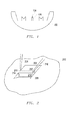
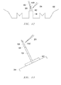
- FIG. 1 shows a typical TEM grid 100, which comprises a partly circular 3 mm ring.
- a sample 104 is attached to a finger 106 of the TEM grid by ion beam deposition or an adhesive.
- the sample extends from the finger 106 so that in a TEM (not shown) an electron beam will have a free path through the sample 104 to a detector under the sample.
- the TEM grid is typically mounted horizontally onto a sample holder in the TEM with the plane of the TEM grid perpendicular to the electron beam, and the sample is observed.
- Some dual beam systems include an ion beam that can be used for extracting the sample, and an electron beam that can be used for SEM or STEM observation.
- the FIB is oriented an angle, such as 52 degrees, from the vertical and an electron beam column is oriented vertically.
- the electron beam column is tilted and the FIB is oriented vertically or also tilted.
- the stage on which the sample is mounted can typically be tilted, in some systems up to about 60 degrees.
- TEM samples can be broadly classified as “planar view” samples or “cross sectional view” samples, depending on how the sample was oriented on the work piece. If the face of the sample to be observed was parallel to the surface of the work piece, the sample is referred to as a "planar view” sample. If the face to be observed was perpendicular to the work piece surface, the sample is referred to as a "cross sectional view” sample.
- FIG. 2 shows a cross-sectional view TEM sample 200 that is partly extracted from a work piece 202 using a typical process.
- An ion beam 204 cuts trenches 206 and 208 on both side of sample to be extracted, leaving a thin lamella 210 having a major surface 212 that will be observed by an electron beam.
- the sample 200 is then freed by tilting the work piece 202 in relation to an ion beam, and cutting around its sides and bottom.
- a probe 216 attaches to the top of the sample 200, before or after it is freed, and transports the sample to a TEM grid.
- FIG. 2 shows sample 200 almost entirely freed, remaining attached by a tab 218 on one side.
- FIG. 2 shows ion beam 204 ready to sever tab 218.
- the major surface 212 is oriented vertically. Transporting the lamella typically does not change its orientation, so its major surfaces are still oriented vertically when the sample 200 is brought to a TEM sample holder.
- the plane of the TEM grid 100 is typically oriented vertically as shown in FIG. 3, so that the sample 200 can be attached to the TEM grid in such a way that major surface 212 extends parallel to the plane of the grid, and the grid structure will not interfere with the transmission of electrons when the grid is mounted in a TEM.
- the ion beam can be used to attach the extracted sample to the TEM grid by ion beam deposition. Once attached, the face of the sample 200 can also be thinned using the ion beam. FIG.
- FIG. 3 shows the sample 200 being attached to the TEM grid 100 in a grid support 302 on a sample stage 304.
- Sample 200 is attached to the TEM grid using an ion beam 204 and a deposition precursor gas 310 from a nozzle 312.
- FIG. 4 shows that the stage 304 is rotated and tilted so that the sample 200 is perpendicular to the ion beam 204 so that the sample 200 can be thinned by the ion beam.
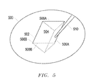
- FIG. 5 shows a work piece 500 from which a planar view sample 502 is being extracted to view a face 504 of the sample.
- the sample 502 is undercut by two intersecting ion beam cuts 506A and 506B from opposite directions, and then the ion beam cuts the sides 508A and 508B to free a "chunk.”
- a probe 510 is attached to the top of the sample 502.
- the extracted sample is therefore oriented horizontally. If the sample were attached in a horizontal orientation to a vertically oriented TEM grid, the sample would extend normal to the plane of the grid, and the grid would interfere with the electron beam of the TEM. If the sample were mounted in a horizontally oriented TEM grid, the face 504 to be observed would face upward. It would then be difficult in a conventional FIB system to thin the back side of the planar sample 502 without removing the TEM grid from the vacuum chamber and flipping it over to expose the back side of sample 502 for thinning.
- flip stage on which the TEM grid can be oriented horizontally for attaching the planar view sample, and then the stage can be flipped 180 degrees and rotated so that the backside of the sample can be presented normal to the ion beam for thinning.
- a flip stage is described for example in U.S. Pat. App. Pub. No. 20040144924 of Asselbergs et al. for "Method for the manufacture and transmissive irradiation of a sample, and particle-optical system” and provides a degree of freedom not available on conventional stages. Such flip stages are not available in all FIB systems.
- An object of the invention is to provide a method and apparatus for altering the orientation of a charged particle beam sample.
- This invention facilitates altering the orientation of a charged particle beam sample in a charged particle beam system and is useful, for example, for preparing a planar view TEM sample.
- a probe comprising a shaft and having an angled tip is attached to the sample. By rotating the shaft through a first angle, the sample orientation is rotated by a second angle. Knowing the orientation of the longitudinal shaft axis with respect to the sample stage plane, and knowing the angle of the probe tip with respect to the longitudinal shaft axis, one can determine an angle of rotation of the shaft that will rotate the sample orientation by precisely ninety degrees or by any other desired angle.
- the sample is orientation is altered by ninety degrees, from horizontal to vertical.
- the sample can be rotated so that it is at a convenient angle for attaching to a TEM grid so that the sample can be thinned by a charged particle beam system without removing the sample from the system for reorientation and without requiring a special stage.
- Reorienting the sample can facilitate subjecting the sample to other processing, such as laser processing or scanning electron beam microscopy, and the invention is not limited to preparing TEM samples.
- FIG. 1 shows a typical TEM grid to which a sample is attached.
- FIG. 2 shows a cross-sectional TEM sample being extracted from a work piece.
- FIG. 3 shows the cross-sectional TEM sample of FIG. 2 being mounted on the TEM grid of FIG. 1.
- FIG. 4 shows the sample and grid of FIG. 3 tilted and rotated for thinning the sample using an ion beam.
- FIG. 5 shows a planar view TEM sample being extracted from a work piece.
- FIG. 6 shows a typical dual beam system used to implement the present invention.
- FIG. 7 is a flow chart showing the steps of a preferred embodiment of the present invention.
- FIG. 8 shows a probe used in a preferred embodiment of the invention.
- FIG. 9 shows the probe of FIG. 8 positioned at the sample 502.
- FIG. 10 shows the probe of FIG. 8 with a sample attached.
- FIG. 11 shows the probe of FIG. 10 rotated 180 degrees to change the orientation of the sample.
- FIG. 12 shows a sample of FIG. 11 being attached to a TEM grid.
- FIG. 13 shows the TEM grid of FIG. 12 on a stage that has been rotated and tilted to orient the sample for ion beam thinning.
- FIG. 14 shows the sample of FIG. 3 partly thinned.
- the invention facilitates preparation of a planar view sample for viewing in TEMs or STEMs.
- the methods provide for extracting and mounting a planar view sample onto a TEM grid in such a manner that the sample can be extracted, attached, and thinned without requiring a flip stage and without requiring that the TEM grid to be removed from the vacuum chamber and reoriented. Re-orienting the sample may also facilitate other analytical or processing operations on the sample.
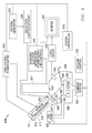
- FIG. 6 shows a typical ion beam system, focused ion beam (FIB) system 610, suitable for practicing the present invention.
- FIB system 610 includes an evacuated envelope having an upper neck portion 612 within which are located a liquid metal ion source 614 or other ion source and a focusing column 616.
- ion sources such as multicusp or other plasma sources, and other optical columns, such as shaped beam columns, could also be used, as well as electron beam and laser system.
- An ion beam 618 passes from liquid metal ion source 614 through ion beam focusing column 616 and between electrostatic deflection means schematically indicated at deflection plates 620 toward work piece 622, which comprises, for example, a semiconductor device positioned on stage 624 within lower chamber 626.
- Stage 624 can also support one or more TEM sample holders, so that a sample can be extracted from the semiconductor device and moved to a TEM sample holder.
- Stage 624 can preferably move in a horizontal plane (X and Y axes) and vertically (Z axis). Stage 624 can also tilt approximately sixty (60) degrees and rotate about the Z axis.
- a system controller 619 controls the operations of the various parts of FIB system 610. Through system controller 619, a user can control ion beam 618 to be scanned in a desired manner through commands entered into a conventional user interface (not shown). Alternatively, system controller 619 may control FIB system 610 in accordance with programmed instructions.
- FIB system 610 incorporates image recognition software, such as software commercially available from Cognex Corporation, Natick, Massachusetts, to automatically identify regions of interest, and then the system can manually or automatically extract samples in accordance with the invention. For example, the system could automatically locate similar features on semiconductor wafers including multiple devices, and take samples of those features on different (or the same) devices.
- An ion pump 628 is employed for evacuating upper neck portion 612.
- the lower chamber 626 is evacuated with turbomolecular and mechanical pumping system 630 under the control of vacuum controller 632.
- the vacuum system provides within lower chamber 626 a vacuum of between approximately 1 x 10 -7 Torr (1.3 x 10 -7 mbar) and 5 x 10 -4 Torr (6.7 x 10 -4 mbar). If an etch-assisting gas, an etch-retarding gas, or a deposition precursor gas is used, the chamber background pressure may rise, typically to about 1 x 10 -5 Torr (1.3 x 10 -5 mbar).
- High voltage power supply 634 is connected to liquid metal ion source 614 as well as to appropriate electrodes in ion beam focusing column 616 for forming an approximately 1 keV to 60 keV ion beam 618 and directing the same toward a sample.
- Deflection controller and amplifier 636 operated in accordance with a prescribed pattern provided by pattern generator 638, is coupled to deflection plates 620 whereby ion beam 618 may be controlled manually or automatically to trace out a corresponding pattern on the upper surface of work piece 622. In some systems the deflection plates are placed before the final lens, as is well known in the art.
- the liquid metal ion source 614 typically provides a metal ion beam of gallium.
- the source typically is capable of being focused into a sub one-tenth micrometer wide beam at work piece 622 for either modifying the work piece 622 by ion milling, enhanced etch, material deposition, or for the purpose of imaging the work piece 622.
- a charged particle detector 640 such as an Everhart Thornley or multi-channel plate, used for detecting secondary ion or electron emission is connected to a video circuit 642 that supplies drive signals to video monitor 644 and receiving deflection signals from controller 619.
- the location of charged particle detector 640 within lower chamber 626 can vary in different embodiments.
- a charged particle detector 640 can be coaxial with the ion beam and include a hole for allowing the ion beam to pass.
- secondary particles can be collected through a final lens and then diverted off axis for collection.
- a scanning electron microscope (SEM) 641, along with its power supply and controls 645, are optionally provided with the FIB system 610.
- a gas delivery system 646 extends into lower chamber 626 for introducing and directing a gaseous vapor toward work piece 622.
- Another gas delivery system is described in U.S. Pat. No. 5,435,850 to Rasmussen for a "Gas Injection System,” also assigned to the assignee of the present invention.
- iodine can be delivered to enhance etching, or a metal organic compound can be delivered to deposit a metal.
- a micromanipulator 647 such as the AutoProbe 200 TM from Omniprobe, Inc., Dallas, Texas, or the Model MM3A from Kleindiek Nanotechnik, Reutlingen, Germany, can precisely move objects within the vacuum chamber.
- Micromanipulator 647 may comprise precision electric motors 648 positioned outside the vacuum chamber to provide X, Y, Z, and theta control of a portion 649 positioned within the vacuum chamber.
- the micromanipulator 647 can be fitted with different end effectors for manipulating small objects.
- the end effector is a thin probe 650.
- the thin probe 650 may be electrically connected to system controller 619 to apply an electric charge to the probe 650 to control the attraction between a sample and the probe.
- a door 660 is opened for inserting work piece 622 onto X-Y stage 624, which may be heated or cooled, and also for servicing an internal gas supply reservoir, if one is used.
- the door is interlocked so that it cannot be opened if the system is under vacuum.
- the high voltage power supply provides an appropriate acceleration voltage to electrodes in ion beam focusing column focusing 616 for energizing and focusing ion beam 618.
- material is sputtered, that is physically ejected, from the sample.
- ion beam 618 can decompose a precursor gas to deposit a material. Focused ion beam systems are commercially available, for example, from FEI Company, Hillsboro, Oregon, the assignee of the present application. While an example of suitable hardware is provided above, the invention is not limited to being implemented in any particular type of hardware.
- FIG. 7 describes the steps of a preferred method of preparing a planar view TEM sample.
- FIG. 5 shows the results of some of the initial steps of FIG. 7.
- a focused ion beam makes a first cut 506A from a first direction in work piece 500 under a sample to be extracted.
- the ion beam makes a second cut 506B under the sample from a second direction, opposite to the first direction and intersecting first cut 506A.
- the sample stage can be rotated 180 degrees and the angle of incidence for the first and second cuts can be the same.
- a left edge is cut 508A intersecting previous cuts 506A and 506B.
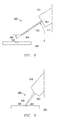
- FIG. 8 shows a probe 800 comprising a shaft 802 having a longitudinal axis 804 and a tip 806 cut at an angle 808 to the longitudinal axis 804.
- Probe shaft 802 is attached to a micromanipulator 810, which can move the shaft in three dimensions and can rotate the shaft.
- the shaft preferably remains at a fixed angle 812, preferably 45 degrees, to the plane of the sample stage in its untilted orientation.
- the probe tip 806 is preferably cut at the same angle as angle 812, so that the flat area of the probe tip is parallel to the plane of the sample stage in its untilted orientation.
- probe tip 806 is attached to the sample 502 as shown in FIG. 9.
- the probe 800 can be attached, for example, using focused ion beam deposition of a metal, such as tungsten, to the sample and the probe.
- a metal such as tungsten
- the probe tip 806 is brought into contact with the sample 502 on major surface 504.
- a precursor gas such as tungsten hexacarbonyl, W(CO) 6 , is directed toward the point of contact between the probe tip 806 and the sample 502, as the ion beam is directed to scan the area around the point of contact.
- the ion beam is used to induce decomposition of the precursor gas to deposit a material that connects the sample 502 to the probe tip 806.
- step 712 the right side wall 508B of the sample is cut, freeing the sample 502.
- probe 800 can be attached to the sample 502 after the right side wall 508B is cut and the sample is freed.
- the probe 800 is withdrawn in step 714 to separate the sample 502 from the work piece 500.
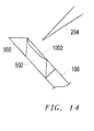
- FIG. 10 shows the sample 502 attached to the probe 800 on major surface 504, opposite to a wedge-shaped backside 1002.
- step 716 the probe shaft 802 is rotated 180 degrees by manipulator 810 as shown in FIG. 11.
- the major surface 504 is then oriented perpendicular to the plane of sample stage 304 and parallel to the plane of a vertically oriented TEM sample holder.
- the sample 502 is then attached using ion beam deposition in step 720 to a finger 106 of the vertically oriented TEM grid 100 as shown in FIG. 12.
- the probe 802 is detached from the sample 502 in step 722, typically using the FIB to sever the connection.
- step 724 the sample stage 304 is rotated as shown in FIG.
- step 726 the back side 1002 of sample 502 is thinned as shown in FIG. 14.
- step 730 the sample is observed in a TEM or an STEM.
- angles and orientations described are useful for a system with an ion beam oriented at an angle to the vertical.
- an ion beam column that is oriented vertically, or at any other angle a skilled person can readily alter the example described above to provide an appropriate embodiment of the invention.
- the invention is useful not only for TEM sample preparation, but can be used for SEM or optical microscope observation, or for any charged particle beam, laser, or other operation on a microscopic specimen.
Landscapes
- Physics & Mathematics (AREA)
- Health & Medical Sciences (AREA)
- Life Sciences & Earth Sciences (AREA)
- Chemical & Material Sciences (AREA)
- Analytical Chemistry (AREA)
- Biochemistry (AREA)
- General Health & Medical Sciences (AREA)
- General Physics & Mathematics (AREA)
- Immunology (AREA)
- Pathology (AREA)
- Sampling And Sample Adjustment (AREA)
- Analysing Materials By The Use Of Radiation (AREA)
Abstract
Description
- The present invention relates to preparation of samples for viewing in charged particle beam systems.
- Charged particle beam microscopy, such as scanning ion microscopy and electron microscopy, provides significantly higher resolution and greater depth of focus than optical microscopy. In a scanning electron microscope (SEM), a primary electron beam is focused to a fine spot that scans the surface to be observed. Secondary electrons are emitted from the surface as it is impacted by the primary electron beam. The secondary electrons are detected, and an image is formed, with the brightness at each point on the image being determined by the number of secondary electrons detected when the beam impacts a corresponding spot on the surface. Scanning ion microscopy (SIM) is similar to scanning electron microscopy, but an ion beam is used to scan the surface and eject the secondary electrons.
- In a transmission electron microscope (TEM), a broad electron beam impacts the sample and electrons that are transmitted through the sample are focused to form an image of the sample. The sample must be sufficiently thin to allow many of the electrons in the primary beam to travel though the sample and exit on the opposite site. Samples are typically less than 100 nm thick.
- In a scanning transmission electron microscope (STEM), a primary electron beam is focused to a fine spot, and the spot is scanned across the sample surface. Electrons that are transmitted through the work piece are collected by an electron detector on the far side of the sample, and the intensity of each point on the image corresponds to the number of electrons collected as the primary beam impacts a corresponding point on the surface.
- Because a sample must be very thin for viewing with transmission electron microscopy (whether TEM or STEM), preparation of the sample can be delicate, time consuming work. The term "TEM" sample as used herein refers to a sample for either a TEM or an STEM and references to preparing a sample for a TEM are to be understood to also include preparing a sample for viewing on an STEM. One method of preparing a TEM sample is to cut the sample from a substrate using an ion beam. A probe is attached to the sample, either before or after the sample has been entirely freed. The probe can be attached, for example, by static electricity, FIB deposition, or an adhesive. The sample, attached to the probe, is moved away from the substrate from which it was extracted and typically attached to a TEM grid using FIB deposition, static electricity, or an adhesive.
- FIG. 1 shows a
typical TEM grid 100, which comprises a partly circular 3 mm ring. In some applications, a sample 104 is attached to afinger 106 of the TEM grid by ion beam deposition or an adhesive. The sample extends from thefinger 106 so that in a TEM (not shown) an electron beam will have a free path through the sample 104 to a detector under the sample. The TEM grid is typically mounted horizontally onto a sample holder in the TEM with the plane of the TEM grid perpendicular to the electron beam, and the sample is observed. - Some dual beam systems include an ion beam that can be used for extracting the sample, and an electron beam that can be used for SEM or STEM observation. In some dual beam systems, the FIB is oriented an angle, such as 52 degrees, from the vertical and an electron beam column is oriented vertically. In other systems, the electron beam column is tilted and the FIB is oriented vertically or also tilted. The stage on which the sample is mounted can typically be tilted, in some systems up to about 60 degrees.
- TEM samples can be broadly classified as "planar view" samples or "cross sectional view" samples, depending on how the sample was oriented on the work piece. If the face of the sample to be observed was parallel to the surface of the work piece, the sample is referred to as a "planar view" sample. If the face to be observed was perpendicular to the work piece surface, the sample is referred to as a "cross sectional view" sample.
- FIG. 2 shows a cross-sectional
view TEM sample 200 that is partly extracted from awork piece 202 using a typical process. Anion beam 204 cutstrenches thin lamella 210 having amajor surface 212 that will be observed by an electron beam. Thesample 200 is then freed by tilting thework piece 202 in relation to an ion beam, and cutting around its sides and bottom. Aprobe 216 attaches to the top of thesample 200, before or after it is freed, and transports the sample to a TEM grid. FIG. 2 showssample 200 almost entirely freed, remaining attached by atab 218 on one side. FIG. 2 showsion beam 204 ready to severtab 218. - As shown in FIG. 2, the
major surface 212 is oriented vertically. Transporting the lamella typically does not change its orientation, so its major surfaces are still oriented vertically when thesample 200 is brought to a TEM sample holder. The plane of theTEM grid 100 is typically oriented vertically as shown in FIG. 3, so that thesample 200 can be attached to the TEM grid in such a way thatmajor surface 212 extends parallel to the plane of the grid, and the grid structure will not interfere with the transmission of electrons when the grid is mounted in a TEM. The ion beam can be used to attach the extracted sample to the TEM grid by ion beam deposition. Once attached, the face of thesample 200 can also be thinned using the ion beam. FIG. 3 shows thesample 200 being attached to theTEM grid 100 in agrid support 302 on asample stage 304.Sample 200 is attached to the TEM grid using anion beam 204 and adeposition precursor gas 310 from anozzle 312. FIG. 4 shows that thestage 304 is rotated and tilted so that thesample 200 is perpendicular to theion beam 204 so that thesample 200 can be thinned by the ion beam. - FIG. 5 shows a
work piece 500 from which aplanar view sample 502 is being extracted to view aface 504 of the sample. Thesample 502 is undercut by two intersectingion beam cuts sides probe 510 is attached to the top of thesample 502. The extracted sample is therefore oriented horizontally. If the sample were attached in a horizontal orientation to a vertically oriented TEM grid, the sample would extend normal to the plane of the grid, and the grid would interfere with the electron beam of the TEM. If the sample were mounted in a horizontally oriented TEM grid, theface 504 to be observed would face upward. It would then be difficult in a conventional FIB system to thin the back side of theplanar sample 502 without removing the TEM grid from the vacuum chamber and flipping it over to expose the back side ofsample 502 for thinning. - This problem of the orientation of a planar
view TEM sample 502 has been overcome in the past by using a "flip stage," on which the TEM grid can be oriented horizontally for attaching the planar view sample, and then the stage can be flipped 180 degrees and rotated so that the backside of the sample can be presented normal to the ion beam for thinning. A flip stage is described for example inU.S. Pat. App. Pub. No. 20040144924 of Asselbergs et al. for "Method for the manufacture and transmissive irradiation of a sample, and particle-optical system" and provides a degree of freedom not available on conventional stages. Such flip stages are not available in all FIB systems. - Thus, it is desirable to provide a method and apparatus for attaching a planar view sample to a TEM grid in a manner such that the sample can be thinned without reorienting the TEM sample holder.
- An object of the invention is to provide a method and apparatus for altering the orientation of a charged particle beam sample.
- This invention facilitates altering the orientation of a charged particle beam sample in a charged particle beam system and is useful, for example, for preparing a planar view TEM sample. In one embodiment, a probe comprising a shaft and having an angled tip is attached to the sample. By rotating the shaft through a first angle, the sample orientation is rotated by a second angle. Knowing the orientation of the longitudinal shaft axis with respect to the sample stage plane, and knowing the angle of the probe tip with respect to the longitudinal shaft axis, one can determine an angle of rotation of the shaft that will rotate the sample orientation by precisely ninety degrees or by any other desired angle. For example, if the longitudinal axis of the shaft is oriented at 45 degrees with respect to the sample stage plane, and the probe tip surface is oriented at 45 degrees with respect to the shaft longitudinal axis, then by rotating the probe shaft 180 degrees, the sample is orientation is altered by ninety degrees, from horizontal to vertical. The sample can be rotated so that it is at a convenient angle for attaching to a TEM grid so that the sample can be thinned by a charged particle beam system without removing the sample from the system for reorientation and without requiring a special stage. Reorienting the sample can facilitate subjecting the sample to other processing, such as laser processing or scanning electron beam microscopy, and the invention is not limited to preparing TEM samples.
- The foregoing has outlined rather broadly the features and technical advantages of the present invention in order that the detailed description of the invention that follows may be better understood. Additional features and advantages of the invention will be described hereinafter. It should be appreciated by those skilled in the art that the conception and specific embodiment disclosed may be readily utilized as a basis for modifying or designing other structures for carrying out the same purposes of the present invention. It should also be realized by those skilled in the art that such equivalent constructions do not depart from the spirit and scope of the invention as set forth in the appended claims.
- For a more through understanding of the present invention, and advantages thereof, reference is now made to the following descriptions taken in conjunction with the accompanying drawings, in which:
- FIG. 1 shows a typical TEM grid to which a sample is attached.
- FIG. 2 shows a cross-sectional TEM sample being extracted from a work piece.
- FIG. 3 shows the cross-sectional TEM sample of FIG. 2 being mounted on the TEM grid of FIG. 1.
- FIG. 4 shows the sample and grid of FIG. 3 tilted and rotated for thinning the sample using an ion beam.
- FIG. 5 shows a planar view TEM sample being extracted from a work piece.
- FIG. 6 shows a typical dual beam system used to implement the present invention.
- FIG. 7 is a flow chart showing the steps of a preferred embodiment of the present invention.
- FIG. 8 shows a probe used in a preferred embodiment of the invention.
- FIG. 9 shows the probe of FIG. 8 positioned at the
sample 502. - FIG. 10 shows the probe of FIG. 8 with a sample attached.
- FIG. 11 shows the probe of FIG. 10 rotated 180 degrees to change the orientation of the sample.
- FIG. 12 shows a sample of FIG. 11 being attached to a TEM grid.
- FIG. 13 shows the TEM grid of FIG. 12 on a stage that has been rotated and tilted to orient the sample for ion beam thinning.
- FIG. 14 shows the sample of FIG. 3 partly thinned.
- This disclosure relates to novel methods for altering the orientation of a sample in a charged particle beam system. In one embodiment, the invention facilitates preparation of a planar view sample for viewing in TEMs or STEMs. The methods provide for extracting and mounting a planar view sample onto a TEM grid in such a manner that the sample can be extracted, attached, and thinned without requiring a flip stage and without requiring that the TEM grid to be removed from the vacuum chamber and reoriented. Re-orienting the sample may also facilitate other analytical or processing operations on the sample.
- FIG. 6 shows a typical ion beam system, focused ion beam (FIB)
system 610, suitable for practicing the present invention.FIB system 610 includes an evacuated envelope having anupper neck portion 612 within which are located a liquidmetal ion source 614 or other ion source and a focusingcolumn 616. Other types of ion sources, such as multicusp or other plasma sources, and other optical columns, such as shaped beam columns, could also be used, as well as electron beam and laser system. - An
ion beam 618 passes from liquidmetal ion source 614 through ionbeam focusing column 616 and between electrostatic deflection means schematically indicated atdeflection plates 620 towardwork piece 622, which comprises, for example, a semiconductor device positioned onstage 624 withinlower chamber 626.Stage 624 can also support one or more TEM sample holders, so that a sample can be extracted from the semiconductor device and moved to a TEM sample holder.Stage 624 can preferably move in a horizontal plane (X and Y axes) and vertically (Z axis).Stage 624 can also tilt approximately sixty (60) degrees and rotate about the Z axis. Asystem controller 619 controls the operations of the various parts ofFIB system 610. Throughsystem controller 619, a user can controlion beam 618 to be scanned in a desired manner through commands entered into a conventional user interface (not shown). Alternatively,system controller 619 may controlFIB system 610 in accordance with programmed instructions. - For example, a user can delineate a region of interest on a display screen using a pointing device, and then the system could automatically perform the steps described below to extract a sample. In some embodiments,
FIB system 610 incorporates image recognition software, such as software commercially available from Cognex Corporation, Natick, Massachusetts, to automatically identify regions of interest, and then the system can manually or automatically extract samples in accordance with the invention. For example, the system could automatically locate similar features on semiconductor wafers including multiple devices, and take samples of those features on different (or the same) devices. - An
ion pump 628 is employed for evacuatingupper neck portion 612. Thelower chamber 626 is evacuated with turbomolecular andmechanical pumping system 630 under the control ofvacuum controller 632. The vacuum system provides within lower chamber 626 a vacuum of between approximately 1 x 10⁻⁷ Torr (1.3 x 10⁻⁷ mbar) and 5 x 10⁻⁴ Torr (6.7 x 10⁻⁴ mbar). If an etch-assisting gas, an etch-retarding gas, or a deposition precursor gas is used, the chamber background pressure may rise, typically to about 1 x 10⁻⁵ Torr (1.3 x 10⁻⁵ mbar). - High
voltage power supply 634 is connected to liquidmetal ion source 614 as well as to appropriate electrodes in ionbeam focusing column 616 for forming an approximately 1 keV to 60keV ion beam 618 and directing the same toward a sample. Deflection controller andamplifier 636, operated in accordance with a prescribed pattern provided bypattern generator 638, is coupled todeflection plates 620 wherebyion beam 618 may be controlled manually or automatically to trace out a corresponding pattern on the upper surface ofwork piece 622. In some systems the deflection plates are placed before the final lens, as is well known in the art. Beam blanking electrodes (no shown) within ionbeam focusing column 616cause ion beam 618 to impact onto blanking aperture (not shown) instead oftarget 622 when a blanking controller (not shown) applies a blanking voltage to the blanking electrode. - The liquid
metal ion source 614 typically provides a metal ion beam of gallium. The source typically is capable of being focused into a sub one-tenth micrometer wide beam atwork piece 622 for either modifying thework piece 622 by ion milling, enhanced etch, material deposition, or for the purpose of imaging thework piece 622. A chargedparticle detector 640, such as an Everhart Thornley or multi-channel plate, used for detecting secondary ion or electron emission is connected to avideo circuit 642 that supplies drive signals to video monitor 644 and receiving deflection signals fromcontroller 619. - The location of charged
particle detector 640 withinlower chamber 626 can vary in different embodiments. For example, a chargedparticle detector 640 can be coaxial with the ion beam and include a hole for allowing the ion beam to pass. In other embodiments, secondary particles can be collected through a final lens and then diverted off axis for collection. A scanning electron microscope (SEM) 641, along with its power supply and controls 645, are optionally provided with theFIB system 610. - A
gas delivery system 646 extends intolower chamber 626 for introducing and directing a gaseous vapor towardwork piece 622.U.S. Pat. No. 5,851,413 to Casella et al. for "Gas Delivery Systems for Particle Beam Processing," assigned to the assignee of the present invention, describes a suitablegas delivery system 646. Another gas delivery system is described inU.S. Pat. No. 5,435,850 to Rasmussen for a "Gas Injection System," also assigned to the assignee of the present invention. For example, iodine can be delivered to enhance etching, or a metal organic compound can be delivered to deposit a metal. - A
micromanipulator 647, such as theAutoProbe 200™ from Omniprobe, Inc., Dallas, Texas, or the Model MM3A from Kleindiek Nanotechnik, Reutlingen, Germany, can precisely move objects within the vacuum chamber.Micromanipulator 647 may comprise precisionelectric motors 648 positioned outside the vacuum chamber to provide X, Y, Z, and theta control of aportion 649 positioned within the vacuum chamber. Themicromanipulator 647 can be fitted with different end effectors for manipulating small objects. In the embodiments described below, the end effector is athin probe 650. Thethin probe 650 may be electrically connected tosystem controller 619 to apply an electric charge to theprobe 650 to control the attraction between a sample and the probe. - A
door 660 is opened for insertingwork piece 622 ontoX-Y stage 624, which may be heated or cooled, and also for servicing an internal gas supply reservoir, if one is used. The door is interlocked so that it cannot be opened if the system is under vacuum. The high voltage power supply provides an appropriate acceleration voltage to electrodes in ion beam focusing column focusing 616 for energizing and focusingion beam 618. When it strikeswork piece 622, material is sputtered, that is physically ejected, from the sample. Alternatively,ion beam 618 can decompose a precursor gas to deposit a material. Focused ion beam systems are commercially available, for example, from FEI Company, Hillsboro, Oregon, the assignee of the present application. While an example of suitable hardware is provided above, the invention is not limited to being implemented in any particular type of hardware. - FIG. 7 describes the steps of a preferred method of preparing a planar view TEM sample. FIG. 5 as described above shows the results of some of the initial steps of FIG. 7. In step 702 a focused ion beam makes a
first cut 506A from a first direction inwork piece 500 under a sample to be extracted. Instep 704, the ion beam makes asecond cut 506B under the sample from a second direction, opposite to the first direction and intersectingfirst cut 506A. For example, the sample stage can be rotated 180 degrees and the angle of incidence for the first and second cuts can be the same. Instep 706, a left edge is cut 508A intersectingprevious cuts - FIG. 8 shows a
probe 800 comprising ashaft 802 having alongitudinal axis 804 and atip 806 cut at anangle 808 to thelongitudinal axis 804. Probeshaft 802 is attached to amicromanipulator 810, which can move the shaft in three dimensions and can rotate the shaft. The shaft preferably remains at afixed angle 812, preferably 45 degrees, to the plane of the sample stage in its untilted orientation. Theprobe tip 806 is preferably cut at the same angle asangle 812, so that the flat area of the probe tip is parallel to the plane of the sample stage in its untilted orientation. Instep 710,probe tip 806 is attached to thesample 502 as shown in FIG. 9. Theprobe 800 can be attached, for example, using focused ion beam deposition of a metal, such as tungsten, to the sample and the probe. To attach theprobe 800 to thesample 502, theprobe tip 806 is brought into contact with thesample 502 onmajor surface 504. A precursor gas, such as tungsten hexacarbonyl, W(CO)6, is directed toward the point of contact between theprobe tip 806 and thesample 502, as the ion beam is directed to scan the area around the point of contact. The ion beam is used to induce decomposition of the precursor gas to deposit a material that connects thesample 502 to theprobe tip 806. - In
step 712, theright side wall 508B of the sample is cut, freeing thesample 502. Alternatively, probe 800 can be attached to thesample 502 after theright side wall 508B is cut and the sample is freed. Next, theprobe 800 is withdrawn instep 714 to separate thesample 502 from thework piece 500.
FIG. 10 shows thesample 502 attached to theprobe 800 onmajor surface 504, opposite to a wedge-shapedbackside 1002. - To view
sample 502 on a TEM, wedge-shapedbackside 1002 must be thinned to reduce the thickness in the center of the wedge. Instep 716, theprobe shaft 802 is rotated 180 degrees bymanipulator 810 as shown in FIG. 11. Themajor surface 504 is then oriented perpendicular to the plane ofsample stage 304 and parallel to the plane of a vertically oriented TEM sample holder. Thesample 502 is then attached using ion beam deposition instep 720 to afinger 106 of the vertically orientedTEM grid 100 as shown in FIG. 12. Theprobe 802 is detached from thesample 502 instep 722, typically using the FIB to sever the connection. Instep 724, thesample stage 304 is rotated as shown in FIG. 13 so that theback side 1002 is facing theion beam 204, andsample stage 304 is tilted so that backside 1002 is perpendicular to the ion beam. The sample is now oriented in a suitable position for thinning by ion beam machining ofback side 1002. Instep 726, theback side 1002 ofsample 502 is thinned as shown in FIG. 14. Instep 730, the sample is observed in a TEM or an STEM. - Skilled persons will also recognize that the flat surface on the bottom of the probe, while preferred, can be eliminated in some embodiments. As long as the sample is fixed to the probe, rotating the probe will re-orient the sample, with the re-orientation angle being determined by the degree of rotation and the angle between the probe axis and the stage plane. Thus, a rounded probe tip, a probe tip angle in which the probe tip is not parallel to the stage plane, or any other probe tip shape, is within the scope of the invention.
- Although the present invention and its advantages have been described in detail, it should be understood that various changes, substitutions and alterations can be made herein without departing from the spirit and scope of the invention as defined by the appended claims. For example, the angles and orientations described are useful for a system with an ion beam oriented at an angle to the vertical. For an ion beam column that is oriented vertically, or at any other angle, a skilled person can readily alter the example described above to provide an appropriate embodiment of the invention. The invention is useful not only for TEM sample preparation, but can be used for SEM or optical microscope observation, or for any charged particle beam, laser, or other operation on a microscopic specimen.
- Moreover, the scope of the present application is not intended to be limited to the particular embodiments of the process, machine, manufacture, composition of matter, means, methods and steps described in the specification. As one of ordinary skill in the art will readily appreciate from the disclosure of the present invention, processes, machines, manufacture, compositions of matter, means, methods, or steps, presently existing or later to be developed that perform substantially the same function or achieve substantially the same result as the corresponding embodiments described herein may be utilized according to the present invention. Accordingly, the appended claims are intended to include within their scope such processes, machines, manufacture, compositions of matter, means, methods, or steps.
- We claim as follows:
Claims (16)
- A method of manipulating a sample in a charged particle beam system, the method comprising:• providing a substrate (202, 622) on a sample stage (624) having a sample stage plane;• freeing a sample (200, 502) from the substrate; and• attaching a probe (216) to the sample;characterized in that• the probe includes a shaft (802) having a shaft axis (804), the shaft axis oriented at a shaft angle (812) in relation to the sample stage plane and the sample having a major surface (212, 504) that is not parallel to the shaft axis; and• rotating the shaft about its axis (804) through a first rotational angle to rotate the sample attached to the probe by an orientational angle.
- The method of claim 1 in which the probe comprises a probe having a probe tip (806) including an attachment surface, the attachment surface orientated at a non-normal tip angle (808) to the shaft axis, and in which attaching the probe to the sample includes attaching the probe with the attachment surface of the probe tip parallel to the sample surface.
- The method of claim 1 or claim 2 in which, after the sample has been rotated by said orientational angle, the sample is attached to a sample holder (100).
- The method of claim 3 in which the sample holder (100) is a TEM grid.
- The method of claim 3 or claim 4 further comprising thinning the sample (200) attached to the sample holder (100) by using an ion beam to create a planar view sample.
- The method of claim 5 further comprising viewing the planar view sample while attached to the sample holder (100) or the TEM grid with a TEM or STEM.
- The method of claim 2 or claim 3 in which the shaft angle (812) is 45 degrees, the tip angle (808) is 45 degrees, the first rotational angle is 180 degrees, and the orientational angle is ninety degrees.
- The method of claim 1, claim 2, or claim 3 in which rotating the shaft axis (804) through a first rotational angle includes rotating the shaft axis by 180 degrees to rotate the sample (502) attached to the probe tip (806) by an orientational angle of 90 degrees.
- The method of claim 2 or claim 3 in which the attachment surface of the tip is oriented parallel to the sample stage plane when the attachment surface of the tip is attached to the sample.
- The method of claim 4, claim 5, or claim 6 in which the sample holder (100) or the TEM grid is oriented vertically.
- The method of claim 1, claim 2, or claim 3 in which attaching the probe (216) to the sample (200) includes attaching the probe to the sample by ion beam deposition.
- The method of claim 1, claim 2, or claim 3 in which attaching the probe (216) to the sample (200) includes attaching the probe to the sample with an adhesive.
- The method of claim 1, claim 2, or claim 3 in which freeing a sample (200, 502) from the substrate (202, 622) comprises freeing the sample from the substrate using a focused ion beam.
- An apparatus (610) for processing a sample, comprising:• an ion beam column (612);• a sample stage (624) having a sample stage plane, the sample stage capable of moving in at least two dimensions, rotating about a vertical axis, and tilting away from the horizontal;characterized by• a probe (650, 810) including a probe shaft (802) having a shaft axis (804) and a probe tip (806) at the end of the probe shaft, the probe tip including an attachment surface for attachment to a sample, said attachment surface oriented at an attachment surface angle that is at a non-normal angle to the shaft axis; and• a micromanipulator (647) for holding and rotating the probe along the shaft axis, the micromanipulator holding the shaft at a shaft angle relative to the sample stage plane, the micromanipulator having a shaft rotation capability such that when the micromanipulator rotates the probe shaft by a shaft rotation angle, the orientation of the probe attachment surface is changed by a sample orientation change angle.
- The apparatus of claim 14 in which the ion beam column (612) is a focused ion beam column.
- The apparatus of claim 14 in which the micromanipulator (647) holds the shaft axis (804) oriented at 45 degrees to the sample stage plane and the probe attachment surface is substantially flat and oriented at an attachment surface angle of 45 degrees to the shaft axis, so that the micromanipulator can be rotated about the shaft axis in order to orient the probe attachment surface to be parallel to the sample stage plane.
Applications Claiming Priority (1)
| Application Number | Priority Date | Filing Date | Title |
|---|---|---|---|
| US11/474,519 US7423263B2 (en) | 2006-06-23 | 2006-06-23 | Planar view sample preparation |
Publications (3)
| Publication Number | Publication Date |
|---|---|
| EP1870691A2 true EP1870691A2 (en) | 2007-12-26 |
| EP1870691A3 EP1870691A3 (en) | 2008-12-10 |
| EP1870691B1 EP1870691B1 (en) | 2016-03-16 |
Family
ID=38535249
Family Applications (1)
| Application Number | Title | Priority Date | Filing Date |
|---|---|---|---|
| EP07110824.5A Active EP1870691B1 (en) | 2006-06-23 | 2007-06-22 | Planar View Sample Preparation |
Country Status (3)
| Country | Link |
|---|---|
| US (1) | US7423263B2 (en) |
| EP (1) | EP1870691B1 (en) |
| JP (1) | JP5086706B2 (en) |
Cited By (10)
| Publication number | Priority date | Publication date | Assignee | Title |
|---|---|---|---|---|
| EP1998356A3 (en) * | 2007-06-01 | 2009-03-11 | FEI Company | In-Situ STEM Sample Preparation |
| US7834315B2 (en) | 2007-04-23 | 2010-11-16 | Omniprobe, Inc. | Method for STEM sample inspection in a charged particle beam instrument |
| WO2011011659A2 (en) * | 2009-07-24 | 2011-01-27 | Omniprobe, Inc. | Variable-tilt tem specimen holder for charged-particle beam instruments |
| WO2011011661A2 (en) * | 2009-07-24 | 2011-01-27 | Omniprobe, Inc. | Method and apparatus for the monitoring of sample milling in a charged particle instrument |
| WO2014055935A1 (en) | 2012-10-05 | 2014-04-10 | Fei Company | Multidimensional structural access |
| US8710464B2 (en) | 2009-03-30 | 2014-04-29 | Hitachi High-Technologies Corporation | Specimen preparation device, and control method in specimen preparation device |
| CN103969104A (en) * | 2014-05-21 | 2014-08-06 | 上海华力微电子有限公司 | Vibration reduction device and method for focusing ion beam machine probe |
| US9082587B2 (en) | 2010-02-17 | 2015-07-14 | Lancaster University Business Enterprises Limited | Method and apparatus for ion beam polishing |
| CN115229316A (en) * | 2022-09-21 | 2022-10-25 | 中国科学院地质与地球物理研究所 | Ion cutting calibration system and method |
| US11658001B1 (en) | 2022-12-07 | 2023-05-23 | Institute Of Geology And Geophysics, Chinese Academy Of Sciences | Ion beam cutting calibration system and method |
Families Citing this family (36)
| Publication number | Priority date | Publication date | Assignee | Title |
|---|---|---|---|---|
| US20060219919A1 (en) * | 2003-11-11 | 2006-10-05 | Moore Thomas M | TEM sample holder and method of forming same |
| US7511282B2 (en) * | 2006-05-25 | 2009-03-31 | Fei Company | Sample preparation |
| JP5266236B2 (en) | 2006-10-20 | 2013-08-21 | エフ・イ−・アイ・カンパニー | Methods and apparatus for sample extraction and handling |
| EP2104864B1 (en) | 2006-10-20 | 2015-03-04 | FEI Company | Method for creating s/tem sample and sample structure |
| WO2009114112A2 (en) * | 2008-03-08 | 2009-09-17 | Omniprobe, Inc. | Method and apparatus for precursor delivery system for irradiation beam instruments |
| US20090296073A1 (en) * | 2008-05-28 | 2009-12-03 | Lam Research Corporation | Method to create three-dimensional images of semiconductor structures using a focused ion beam device and a scanning electron microscope |
| US8288740B2 (en) * | 2008-06-27 | 2012-10-16 | Omniprobe, Inc. | Method for preparing specimens for atom probe analysis and specimen assemblies made thereby |
| WO2010014252A2 (en) * | 2008-08-01 | 2010-02-04 | Omniprobe, Inc. | Grid holder for stem analysis in a charged particle instrument |
| DE102008042179B9 (en) * | 2008-09-17 | 2013-10-10 | Carl Zeiss Microscopy Gmbh | Method for analyzing a sample |
| DE102008052006B4 (en) * | 2008-10-10 | 2018-12-20 | 3D-Micromac Ag | Method and device for the production of samples for transmission electron microscopy |
| JP5378830B2 (en) * | 2009-02-20 | 2013-12-25 | 株式会社日立ハイテクサイエンス | Focused ion beam apparatus and sample processing method using the same |
| US8347741B2 (en) | 2010-06-01 | 2013-01-08 | International Business Machines Corporation | Specimen handling apparatus |
| US8721907B2 (en) * | 2010-10-31 | 2014-05-13 | Camtek Ltd. | Method and system for milling and imaging an object |
| CN103403520B (en) | 2011-01-28 | 2015-12-23 | Fei公司 | Prepared by TEM sample |
| US8859963B2 (en) * | 2011-06-03 | 2014-10-14 | Fei Company | Methods for preparing thin samples for TEM imaging |
| EP2749863A3 (en) * | 2012-12-31 | 2016-05-04 | Fei Company | Method for preparing samples for imaging |
| US8912490B2 (en) * | 2011-06-03 | 2014-12-16 | Fei Company | Method for preparing samples for imaging |
| EP2786113B1 (en) * | 2011-12-01 | 2017-03-01 | FEI Company | High throughput tem preparation process for backside thinning of cross-sectional view lamella |
| JP5872922B2 (en) * | 2012-02-21 | 2016-03-01 | 株式会社日立ハイテクサイエンス | Sample preparation method and apparatus |
| US8740209B2 (en) * | 2012-02-22 | 2014-06-03 | Expresslo Llc | Method and apparatus for ex-situ lift-out specimen preparation |
| GB201308436D0 (en) * | 2013-05-10 | 2013-06-19 | Oxford Instr Nanotechnology Tools Ltd | Metrology for preparation of thin samples |
| US9040908B2 (en) | 2013-06-28 | 2015-05-26 | Fei Company | Plan view sample preparation |
| EP2930736A1 (en) * | 2014-04-10 | 2015-10-14 | Centre National De La Recherche Scientifique | Sample holding micro vice and sample holding system for coupled transmission electron microscopy (TEM) and atom-probe tomography (APT) analyses |
| US9281163B2 (en) | 2014-04-14 | 2016-03-08 | Fei Company | High capacity TEM grid |
| JP6542608B2 (en) * | 2014-08-29 | 2019-07-10 | 株式会社日立ハイテクサイエンス | Charged particle beam device |
| KR102358551B1 (en) * | 2014-08-29 | 2022-02-04 | 가부시키가이샤 히다치 하이테크 사이언스 | Automatic sample strip manufacturing apparatus |
| US20160189929A1 (en) * | 2014-10-29 | 2016-06-30 | Omniprobe, Inc. | Rapid tem sample preparation method with backside fib milling |
| KR102489385B1 (en) * | 2015-02-19 | 2023-01-17 | 가부시키가이샤 히다치 하이테크 사이언스 | Charged particle beam apparatus |
| CN105158516B (en) * | 2015-08-20 | 2018-10-16 | 上海华力微电子有限公司 | The preparation method of transmission electron microscope planar sample in a kind of Integrated circuit analysis |
| US10546719B2 (en) | 2017-06-02 | 2020-01-28 | Fei Company | Face-on, gas-assisted etching for plan-view lamellae preparation |
| CZ2018157A3 (en) * | 2018-03-29 | 2019-10-09 | Tescan Brno, S.R.O. | Device for creating and placing a lamella |
| DE102018212511B4 (en) * | 2018-07-26 | 2020-02-06 | Carl Zeiss Microscopy Gmbh | Recording device, sample holder system and method for preparing microscopic samples |
| DE102020203580B4 (en) | 2020-03-20 | 2021-10-07 | Carl Zeiss Microscopy Gmbh | Method for changing the spatial orientation of a microsample in a microscope system, as well as computer program product |
| EP4068333A1 (en) * | 2021-03-31 | 2022-10-05 | FEI Company | Sample carrier for use in a charged particle microscope, and a method of using such a sample carrier in a charged particle microscope |
| US12085522B2 (en) | 2021-07-08 | 2024-09-10 | Changxin Memory Technologies, Inc. | Sample rotation system and method |
| CN114279784A (en) * | 2021-12-22 | 2022-04-05 | 上海季丰电子股份有限公司 | Preparation method of transmission electron microscope sample |
Citations (6)
| Publication number | Priority date | Publication date | Assignee | Title |
|---|---|---|---|---|
| EP1204133A2 (en) * | 2000-11-02 | 2002-05-08 | Hitachi, Ltd. | Method and apparatus for processing a micro sample |
| US20020166976A1 (en) * | 2001-05-08 | 2002-11-14 | Masakazu Sugaya | Beam as well as method and equipment for specimen fabrication |
| US20040246465A1 (en) * | 2003-05-06 | 2004-12-09 | Kouji Iwasaki | Micro-sample pick-up apparatus and micro-sample pick-up method |
| JP2005345220A (en) * | 2004-06-02 | 2005-12-15 | Hitachi High-Technologies Corp | Device and method for sample preparation |
| US20060011868A1 (en) * | 2004-07-14 | 2006-01-19 | Applied Materials Israel Ltd | Method and apparatus for sample formation and microanalysis in a vacuum chamber |
| US7041985B1 (en) * | 2004-11-12 | 2006-05-09 | Western Digital (Fremont), Inc. | Manipulator for microscopy sample preparation and methods for making and use thereof |
Family Cites Families (17)
| Publication number | Priority date | Publication date | Assignee | Title |
|---|---|---|---|---|
| JP2774884B2 (en) * | 1991-08-22 | 1998-07-09 | 株式会社日立製作所 | Method for separating sample and method for analyzing separated sample obtained by this separation method |
| US5435850A (en) * | 1993-09-17 | 1995-07-25 | Fei Company | Gas injection system |
| US5851413A (en) * | 1996-06-19 | 1998-12-22 | Micrion Corporation | Gas delivery systems for particle beam processing |
| JP3547143B2 (en) * | 1997-07-22 | 2004-07-28 | 株式会社日立製作所 | Sample preparation method |
| JPH11108813A (en) * | 1997-10-03 | 1999-04-23 | Hitachi Ltd | Method and device for preparing sample |
| US6140652A (en) * | 1998-09-09 | 2000-10-31 | Intersil Corporation | Device containing sample preparation sites for transmission electron microscopic analysis and processes of formation and use |
| JP2001311681A (en) * | 2000-04-28 | 2001-11-09 | Nippon Steel Corp | Method for preparing sample for transmission electron microscope observation and sampling apparatus |
| US6420722B2 (en) * | 2000-05-22 | 2002-07-16 | Omniprobe, Inc. | Method for sample separation and lift-out with one cut |
| WO2002071031A1 (en) * | 2001-03-01 | 2002-09-12 | Moore Thomas M | Total release method for sample extraction from a charged particle instrument |
| JP2004093353A (en) * | 2002-08-30 | 2004-03-25 | Seiko Instruments Inc | Sample preparation device |
| NL1022426C2 (en) * | 2003-01-17 | 2004-07-26 | Fei Co | Method for the manufacture and transmissive irradiation of a preparation and particle optical system. |
| US6864552B2 (en) * | 2003-01-21 | 2005-03-08 | Mp Technologies, Llc | Focal plane arrays in type II-superlattices |
| US6995380B2 (en) * | 2003-03-13 | 2006-02-07 | Ascend Instruments, Llc | End effector for supporting a microsample |
| JP4297736B2 (en) * | 2003-06-11 | 2009-07-15 | 株式会社日立ハイテクノロジーズ | Focused ion beam device |
| DE602005019498D1 (en) | 2004-07-01 | 2010-04-08 | Fei Co | Method for removing a microscopic sample from a substrate |
| DE602005000352T2 (en) * | 2004-07-01 | 2007-05-10 | Fei Co., Hillsboro | Method for taking a microscopic sample from a substrate |
| JP4259454B2 (en) * | 2004-11-01 | 2009-04-30 | 株式会社日立製作所 | Micro-sample processing observation equipment |
-
2006
- 2006-06-23 US US11/474,519 patent/US7423263B2/en active Active
-
2007
- 2007-06-21 JP JP2007163546A patent/JP5086706B2/en active Active
- 2007-06-22 EP EP07110824.5A patent/EP1870691B1/en active Active
Patent Citations (6)
| Publication number | Priority date | Publication date | Assignee | Title |
|---|---|---|---|---|
| EP1204133A2 (en) * | 2000-11-02 | 2002-05-08 | Hitachi, Ltd. | Method and apparatus for processing a micro sample |
| US20020166976A1 (en) * | 2001-05-08 | 2002-11-14 | Masakazu Sugaya | Beam as well as method and equipment for specimen fabrication |
| US20040246465A1 (en) * | 2003-05-06 | 2004-12-09 | Kouji Iwasaki | Micro-sample pick-up apparatus and micro-sample pick-up method |
| JP2005345220A (en) * | 2004-06-02 | 2005-12-15 | Hitachi High-Technologies Corp | Device and method for sample preparation |
| US20060011868A1 (en) * | 2004-07-14 | 2006-01-19 | Applied Materials Israel Ltd | Method and apparatus for sample formation and microanalysis in a vacuum chamber |
| US7041985B1 (en) * | 2004-11-12 | 2006-05-09 | Western Digital (Fremont), Inc. | Manipulator for microscopy sample preparation and methods for making and use thereof |
Cited By (16)
| Publication number | Priority date | Publication date | Assignee | Title |
|---|---|---|---|---|
| US7834315B2 (en) | 2007-04-23 | 2010-11-16 | Omniprobe, Inc. | Method for STEM sample inspection in a charged particle beam instrument |
| USRE46350E1 (en) | 2007-04-23 | 2017-03-28 | Omniprobe, Inc. | Method for stem sample inspection in a charged particle beam instrument |
| EP1998356A3 (en) * | 2007-06-01 | 2009-03-11 | FEI Company | In-Situ STEM Sample Preparation |
| US8710464B2 (en) | 2009-03-30 | 2014-04-29 | Hitachi High-Technologies Corporation | Specimen preparation device, and control method in specimen preparation device |
| WO2011011659A3 (en) * | 2009-07-24 | 2011-04-28 | Omniprobe, Inc. | Variable-tilt tem specimen holder for charged-particle beam instruments |
| WO2011011661A3 (en) * | 2009-07-24 | 2011-04-28 | Omniprobe, Inc. | Method and apparatus for the monitoring of sample milling in a charged particle instrument |
| US8227781B2 (en) | 2009-07-24 | 2012-07-24 | Lyudmila Zaykova-Feldman | Variable-tilt specimen holder and method and for monitoring milling in a charged-particle instrument |
| WO2011011661A2 (en) * | 2009-07-24 | 2011-01-27 | Omniprobe, Inc. | Method and apparatus for the monitoring of sample milling in a charged particle instrument |
| WO2011011659A2 (en) * | 2009-07-24 | 2011-01-27 | Omniprobe, Inc. | Variable-tilt tem specimen holder for charged-particle beam instruments |
| US9082587B2 (en) | 2010-02-17 | 2015-07-14 | Lancaster University Business Enterprises Limited | Method and apparatus for ion beam polishing |
| WO2014055935A1 (en) | 2012-10-05 | 2014-04-10 | Fei Company | Multidimensional structural access |
| EP2904633A4 (en) * | 2012-10-05 | 2016-03-02 | Fei Co | Multidimensional structural access |
| CN103969104A (en) * | 2014-05-21 | 2014-08-06 | 上海华力微电子有限公司 | Vibration reduction device and method for focusing ion beam machine probe |
| CN115229316A (en) * | 2022-09-21 | 2022-10-25 | 中国科学院地质与地球物理研究所 | Ion cutting calibration system and method |
| CN115229316B (en) * | 2022-09-21 | 2022-11-22 | 中国科学院地质与地球物理研究所 | Ion cutting calibration system and method |
| US11658001B1 (en) | 2022-12-07 | 2023-05-23 | Institute Of Geology And Geophysics, Chinese Academy Of Sciences | Ion beam cutting calibration system and method |
Also Published As
| Publication number | Publication date |
|---|---|
| JP5086706B2 (en) | 2012-11-28 |
| US20080073535A1 (en) | 2008-03-27 |
| EP1870691B1 (en) | 2016-03-16 |
| EP1870691A3 (en) | 2008-12-10 |
| US7423263B2 (en) | 2008-09-09 |
| JP2008026312A (en) | 2008-02-07 |
Similar Documents
| Publication | Publication Date | Title |
|---|---|---|
| US7423263B2 (en) | Planar view sample preparation | |
| US10283317B2 (en) | High throughput TEM preparation processes and hardware for backside thinning of cross-sectional view lamella | |
| US9368325B2 (en) | TEM sample preparation | |
| EP1998356B1 (en) | In-Situ STEM Sample Preparation | |
| US7511282B2 (en) | Sample preparation | |
| US7442924B2 (en) | Repetitive circumferential milling for sample preparation | |
| US9177760B2 (en) | TEM sample preparation | |
| US5270552A (en) | Method for separating specimen and method for analyzing the specimen separated by the specimen separating method | |
| EP2933821B1 (en) | High capacity tem grid | |
| US20230358696A1 (en) | Method for cross-section sample preparation | |
| US9837246B1 (en) | Reinforced sample for transmission electron microscope | |
| EP2837926B1 (en) | Detaching probe from TEM sample during sample preparation |
Legal Events
| Date | Code | Title | Description |
|---|---|---|---|
| PUAI | Public reference made under article 153(3) epc to a published international application that has entered the european phase |
Free format text: ORIGINAL CODE: 0009012 |
|
| 17P | Request for examination filed |
Effective date: 20070622 |
|
| AK | Designated contracting states |
Kind code of ref document: A2 Designated state(s): AT BE BG CH CY CZ DE DK EE ES FI FR GB GR HU IE IS IT LI LT LU LV MC MT NL PL PT RO SE SI SK TR |
|
| AX | Request for extension of the european patent |
Extension state: AL BA HR MK YU |
|
| PUAL | Search report despatched |
Free format text: ORIGINAL CODE: 0009013 |
|
| AK | Designated contracting states |
Kind code of ref document: A3 Designated state(s): AT BE BG CH CY CZ DE DK EE ES FI FR GB GR HU IE IS IT LI LT LU LV MC MT NL PL PT RO SE SI SK TR |
|
| AX | Request for extension of the european patent |
Extension state: AL BA HR MK RS |
|
| 17Q | First examination report despatched |
Effective date: 20090629 |
|
| AKX | Designation fees paid |
Designated state(s): AT BE BG CH CY CZ DE DK EE ES FI FR GB GR HU IE IS IT LI LT LU LV MC MT NL PL PT RO SE SI SK TR |
|
| GRAP | Despatch of communication of intention to grant a patent |
Free format text: ORIGINAL CODE: EPIDOSNIGR1 |
|
| INTG | Intention to grant announced |
Effective date: 20151112 |
|
| GRAS | Grant fee paid |
Free format text: ORIGINAL CODE: EPIDOSNIGR3 |
|
| GRAA | (expected) grant |
Free format text: ORIGINAL CODE: 0009210 |
|
| AK | Designated contracting states |
Kind code of ref document: B1 Designated state(s): AT BE BG CH CY CZ DE DK EE ES FI FR GB GR HU IE IS IT LI LT LU LV MC MT NL PL PT RO SE SI SK TR |
|
| REG | Reference to a national code |
Ref country code: GB Ref legal event code: FG4D |
|
| REG | Reference to a national code |
Ref country code: CH Ref legal event code: EP |
|
| REG | Reference to a national code |
Ref country code: IE Ref legal event code: FG4D |
|
| REG | Reference to a national code |
Ref country code: AT Ref legal event code: REF Ref document number: 781659 Country of ref document: AT Kind code of ref document: T Effective date: 20160415 |
|
| REG | Reference to a national code |
Ref country code: DE Ref legal event code: R096 Ref document number: 602007045275 Country of ref document: DE |
|
| REG | Reference to a national code |
Ref country code: FR Ref legal event code: PLFP Year of fee payment: 10 |
|
| REG | Reference to a national code |
Ref country code: NL Ref legal event code: MP Effective date: 20160316 |
|
| REG | Reference to a national code |
Ref country code: LT Ref legal event code: MG4D |
|
| PG25 | Lapsed in a contracting state [announced via postgrant information from national office to epo] |
Ref country code: FI Free format text: LAPSE BECAUSE OF FAILURE TO SUBMIT A TRANSLATION OF THE DESCRIPTION OR TO PAY THE FEE WITHIN THE PRESCRIBED TIME-LIMIT Effective date: 20160316 Ref country code: GR Free format text: LAPSE BECAUSE OF FAILURE TO SUBMIT A TRANSLATION OF THE DESCRIPTION OR TO PAY THE FEE WITHIN THE PRESCRIBED TIME-LIMIT Effective date: 20160617 |
|
| REG | Reference to a national code |
Ref country code: AT Ref legal event code: MK05 Ref document number: 781659 Country of ref document: AT Kind code of ref document: T Effective date: 20160316 |
|
| PG25 | Lapsed in a contracting state [announced via postgrant information from national office to epo] |
Ref country code: LV Free format text: LAPSE BECAUSE OF FAILURE TO SUBMIT A TRANSLATION OF THE DESCRIPTION OR TO PAY THE FEE WITHIN THE PRESCRIBED TIME-LIMIT Effective date: 20160316 Ref country code: SE Free format text: LAPSE BECAUSE OF FAILURE TO SUBMIT A TRANSLATION OF THE DESCRIPTION OR TO PAY THE FEE WITHIN THE PRESCRIBED TIME-LIMIT Effective date: 20160316 Ref country code: LT Free format text: LAPSE BECAUSE OF FAILURE TO SUBMIT A TRANSLATION OF THE DESCRIPTION OR TO PAY THE FEE WITHIN THE PRESCRIBED TIME-LIMIT Effective date: 20160316 Ref country code: NL Free format text: LAPSE BECAUSE OF FAILURE TO SUBMIT A TRANSLATION OF THE DESCRIPTION OR TO PAY THE FEE WITHIN THE PRESCRIBED TIME-LIMIT Effective date: 20160316 |
|
| PG25 | Lapsed in a contracting state [announced via postgrant information from national office to epo] |
Ref country code: PL Free format text: LAPSE BECAUSE OF FAILURE TO SUBMIT A TRANSLATION OF THE DESCRIPTION OR TO PAY THE FEE WITHIN THE PRESCRIBED TIME-LIMIT Effective date: 20160316 Ref country code: IS Free format text: LAPSE BECAUSE OF FAILURE TO SUBMIT A TRANSLATION OF THE DESCRIPTION OR TO PAY THE FEE WITHIN THE PRESCRIBED TIME-LIMIT Effective date: 20160716 Ref country code: EE Free format text: LAPSE BECAUSE OF FAILURE TO SUBMIT A TRANSLATION OF THE DESCRIPTION OR TO PAY THE FEE WITHIN THE PRESCRIBED TIME-LIMIT Effective date: 20160316 |
|
| PG25 | Lapsed in a contracting state [announced via postgrant information from national office to epo] |
Ref country code: PT Free format text: LAPSE BECAUSE OF FAILURE TO SUBMIT A TRANSLATION OF THE DESCRIPTION OR TO PAY THE FEE WITHIN THE PRESCRIBED TIME-LIMIT Effective date: 20160718 Ref country code: AT Free format text: LAPSE BECAUSE OF FAILURE TO SUBMIT A TRANSLATION OF THE DESCRIPTION OR TO PAY THE FEE WITHIN THE PRESCRIBED TIME-LIMIT Effective date: 20160316 Ref country code: RO Free format text: LAPSE BECAUSE OF FAILURE TO SUBMIT A TRANSLATION OF THE DESCRIPTION OR TO PAY THE FEE WITHIN THE PRESCRIBED TIME-LIMIT Effective date: 20160316 Ref country code: SK Free format text: LAPSE BECAUSE OF FAILURE TO SUBMIT A TRANSLATION OF THE DESCRIPTION OR TO PAY THE FEE WITHIN THE PRESCRIBED TIME-LIMIT Effective date: 20160316 Ref country code: CZ Free format text: LAPSE BECAUSE OF FAILURE TO SUBMIT A TRANSLATION OF THE DESCRIPTION OR TO PAY THE FEE WITHIN THE PRESCRIBED TIME-LIMIT Effective date: 20160316 Ref country code: ES Free format text: LAPSE BECAUSE OF FAILURE TO SUBMIT A TRANSLATION OF THE DESCRIPTION OR TO PAY THE FEE WITHIN THE PRESCRIBED TIME-LIMIT Effective date: 20160316 |
|
| REG | Reference to a national code |
Ref country code: DE Ref legal event code: R097 Ref document number: 602007045275 Country of ref document: DE |
|
| PG25 | Lapsed in a contracting state [announced via postgrant information from national office to epo] |
Ref country code: BE Free format text: LAPSE BECAUSE OF FAILURE TO SUBMIT A TRANSLATION OF THE DESCRIPTION OR TO PAY THE FEE WITHIN THE PRESCRIBED TIME-LIMIT Effective date: 20160316 Ref country code: IT Free format text: LAPSE BECAUSE OF FAILURE TO SUBMIT A TRANSLATION OF THE DESCRIPTION OR TO PAY THE FEE WITHIN THE PRESCRIBED TIME-LIMIT Effective date: 20160316 |
|
| PLBE | No opposition filed within time limit |
Free format text: ORIGINAL CODE: 0009261 |
|
| STAA | Information on the status of an ep patent application or granted ep patent |
Free format text: STATUS: NO OPPOSITION FILED WITHIN TIME LIMIT |
|
| PG25 | Lapsed in a contracting state [announced via postgrant information from national office to epo] |
Ref country code: DK Free format text: LAPSE BECAUSE OF FAILURE TO SUBMIT A TRANSLATION OF THE DESCRIPTION OR TO PAY THE FEE WITHIN THE PRESCRIBED TIME-LIMIT Effective date: 20160316 Ref country code: MC Free format text: LAPSE BECAUSE OF FAILURE TO SUBMIT A TRANSLATION OF THE DESCRIPTION OR TO PAY THE FEE WITHIN THE PRESCRIBED TIME-LIMIT Effective date: 20160316 |
|
| REG | Reference to a national code |
Ref country code: CH Ref legal event code: PL |
|
| 26N | No opposition filed |
Effective date: 20161219 |
|
| PG25 | Lapsed in a contracting state [announced via postgrant information from national office to epo] |
Ref country code: BG Free format text: LAPSE BECAUSE OF FAILURE TO SUBMIT A TRANSLATION OF THE DESCRIPTION OR TO PAY THE FEE WITHIN THE PRESCRIBED TIME-LIMIT Effective date: 20160616 |
|
| REG | Reference to a national code |
Ref country code: IE Ref legal event code: MM4A |
|
| PG25 | Lapsed in a contracting state [announced via postgrant information from national office to epo] |
Ref country code: CH Free format text: LAPSE BECAUSE OF NON-PAYMENT OF DUE FEES Effective date: 20160630 Ref country code: LI Free format text: LAPSE BECAUSE OF NON-PAYMENT OF DUE FEES Effective date: 20160630 |
|
| REG | Reference to a national code |
Ref country code: FR Ref legal event code: PLFP Year of fee payment: 11 |
|
| PG25 | Lapsed in a contracting state [announced via postgrant information from national office to epo] |
Ref country code: SI Free format text: LAPSE BECAUSE OF FAILURE TO SUBMIT A TRANSLATION OF THE DESCRIPTION OR TO PAY THE FEE WITHIN THE PRESCRIBED TIME-LIMIT Effective date: 20160316 Ref country code: IE Free format text: LAPSE BECAUSE OF NON-PAYMENT OF DUE FEES Effective date: 20160622 |
|
| REG | Reference to a national code |
Ref country code: FR Ref legal event code: PLFP Year of fee payment: 12 |
|
| PG25 | Lapsed in a contracting state [announced via postgrant information from national office to epo] |
Ref country code: HU Free format text: LAPSE BECAUSE OF FAILURE TO SUBMIT A TRANSLATION OF THE DESCRIPTION OR TO PAY THE FEE WITHIN THE PRESCRIBED TIME-LIMIT; INVALID AB INITIO Effective date: 20070622 Ref country code: CY Free format text: LAPSE BECAUSE OF FAILURE TO SUBMIT A TRANSLATION OF THE DESCRIPTION OR TO PAY THE FEE WITHIN THE PRESCRIBED TIME-LIMIT Effective date: 20160316 |
|
| PG25 | Lapsed in a contracting state [announced via postgrant information from national office to epo] |
Ref country code: MT Free format text: LAPSE BECAUSE OF NON-PAYMENT OF DUE FEES Effective date: 20160630 Ref country code: LU Free format text: LAPSE BECAUSE OF NON-PAYMENT OF DUE FEES Effective date: 20160622 Ref country code: TR Free format text: LAPSE BECAUSE OF FAILURE TO SUBMIT A TRANSLATION OF THE DESCRIPTION OR TO PAY THE FEE WITHIN THE PRESCRIBED TIME-LIMIT Effective date: 20160316 |
|
| P01 | Opt-out of the competence of the unified patent court (upc) registered |
Effective date: 20230520 |
|
| PGFP | Annual fee paid to national office [announced via postgrant information from national office to epo] |
Ref country code: GB Payment date: 20240621 Year of fee payment: 18 |
|
| PGFP | Annual fee paid to national office [announced via postgrant information from national office to epo] |
Ref country code: DE Payment date: 20240611 Year of fee payment: 18 |
|
| PGFP | Annual fee paid to national office [announced via postgrant information from national office to epo] |
Ref country code: FR Payment date: 20240627 Year of fee payment: 18 |