JP3547143B2 - Sample preparation method - Google Patents
Sample preparation method Download PDFInfo
- Publication number
- JP3547143B2 JP3547143B2 JP50845799A JP50845799A JP3547143B2 JP 3547143 B2 JP3547143 B2 JP 3547143B2 JP 50845799 A JP50845799 A JP 50845799A JP 50845799 A JP50845799 A JP 50845799A JP 3547143 B2 JP3547143 B2 JP 3547143B2
- Authority
- JP
- Japan
- Prior art keywords
- sample
- probe
- substrate
- piece
- ion beam
- Prior art date
- Legal status (The legal status is an assumption and is not a legal conclusion. Google has not performed a legal analysis and makes no representation as to the accuracy of the status listed.)
- Expired - Lifetime
Links
Images


Classifications
-
- H—ELECTRICITY
- H01—ELECTRIC ELEMENTS
- H01J—ELECTRIC DISCHARGE TUBES OR DISCHARGE LAMPS
- H01J37/00—Discharge tubes with provision for introducing objects or material to be exposed to the discharge, e.g. for the purpose of examination or processing thereof
- H01J37/30—Electron-beam or ion-beam tubes for localised treatment of objects
- H01J37/305—Electron-beam or ion-beam tubes for localised treatment of objects for casting, melting, evaporating or etching
- H01J37/3053—Electron-beam or ion-beam tubes for localised treatment of objects for casting, melting, evaporating or etching for evaporating or etching
- H01J37/3056—Electron-beam or ion-beam tubes for localised treatment of objects for casting, melting, evaporating or etching for evaporating or etching for microworking, e.g. etching of gratings, trimming of electrical components
-
- G—PHYSICS
- G01—MEASURING; TESTING
- G01N—INVESTIGATING OR ANALYSING MATERIALS BY DETERMINING THEIR CHEMICAL OR PHYSICAL PROPERTIES
- G01N1/00—Sampling; Preparing specimens for investigation
- G01N1/28—Preparing specimens for investigation including physical details of (bio-)chemical methods covered elsewhere, e.g. G01N33/50, C12Q
- G01N1/286—Preparing specimens for investigation including physical details of (bio-)chemical methods covered elsewhere, e.g. G01N33/50, C12Q involving mechanical work, e.g. chopping, disintegrating, compacting, homogenising
-
- G—PHYSICS
- G01—MEASURING; TESTING
- G01N—INVESTIGATING OR ANALYSING MATERIALS BY DETERMINING THEIR CHEMICAL OR PHYSICAL PROPERTIES
- G01N1/00—Sampling; Preparing specimens for investigation
- G01N1/28—Preparing specimens for investigation including physical details of (bio-)chemical methods covered elsewhere, e.g. G01N33/50, C12Q
- G01N1/32—Polishing; Etching
-
- G—PHYSICS
- G01—MEASURING; TESTING
- G01N—INVESTIGATING OR ANALYSING MATERIALS BY DETERMINING THEIR CHEMICAL OR PHYSICAL PROPERTIES
- G01N1/00—Sampling; Preparing specimens for investigation
- G01N1/02—Devices for withdrawing samples
- G01N2001/028—Sampling from a surface, swabbing, vaporising
-
- G—PHYSICS
- G01—MEASURING; TESTING
- G01N—INVESTIGATING OR ANALYSING MATERIALS BY DETERMINING THEIR CHEMICAL OR PHYSICAL PROPERTIES
- G01N1/00—Sampling; Preparing specimens for investigation
- G01N1/02—Devices for withdrawing samples
- G01N1/04—Devices for withdrawing samples in the solid state, e.g. by cutting
- G01N2001/045—Laser ablation; Microwave vaporisation
-
- G—PHYSICS
- G01—MEASURING; TESTING
- G01N—INVESTIGATING OR ANALYSING MATERIALS BY DETERMINING THEIR CHEMICAL OR PHYSICAL PROPERTIES
- G01N1/00—Sampling; Preparing specimens for investigation
- G01N1/28—Preparing specimens for investigation including physical details of (bio-)chemical methods covered elsewhere, e.g. G01N33/50, C12Q
- G01N1/2813—Producing thin layers of samples on a substrate, e.g. smearing, spinning-on
- G01N2001/282—Producing thin layers of samples on a substrate, e.g. smearing, spinning-on with mapping; Identification of areas; Spatial correlated pattern
-
- G—PHYSICS
- G01—MEASURING; TESTING
- G01N—INVESTIGATING OR ANALYSING MATERIALS BY DETERMINING THEIR CHEMICAL OR PHYSICAL PROPERTIES
- G01N1/00—Sampling; Preparing specimens for investigation
- G01N1/28—Preparing specimens for investigation including physical details of (bio-)chemical methods covered elsewhere, e.g. G01N33/50, C12Q
- G01N1/286—Preparing specimens for investigation including physical details of (bio-)chemical methods covered elsewhere, e.g. G01N33/50, C12Q involving mechanical work, e.g. chopping, disintegrating, compacting, homogenising
- G01N2001/2873—Cutting or cleaving
- G01N2001/2886—Laser cutting, e.g. tissue catapult
-
- H—ELECTRICITY
- H01—ELECTRIC ELEMENTS
- H01J—ELECTRIC DISCHARGE TUBES OR DISCHARGE LAMPS
- H01J2237/00—Discharge tubes exposing object to beam, e.g. for analysis treatment, etching, imaging
- H01J2237/30—Electron or ion beam tubes for processing objects
- H01J2237/317—Processing objects on a microscale
- H01J2237/3174—Etching microareas
- H01J2237/31745—Etching microareas for preparing specimen to be viewed in microscopes or analyzed in microanalysers
-
- Y—GENERAL TAGGING OF NEW TECHNOLOGICAL DEVELOPMENTS; GENERAL TAGGING OF CROSS-SECTIONAL TECHNOLOGIES SPANNING OVER SEVERAL SECTIONS OF THE IPC; TECHNICAL SUBJECTS COVERED BY FORMER USPC CROSS-REFERENCE ART COLLECTIONS [XRACs] AND DIGESTS
- Y10—TECHNICAL SUBJECTS COVERED BY FORMER USPC
- Y10S—TECHNICAL SUBJECTS COVERED BY FORMER USPC CROSS-REFERENCE ART COLLECTIONS [XRACs] AND DIGESTS
- Y10S977/00—Nanotechnology
- Y10S977/902—Specified use of nanostructure
- Y10S977/932—Specified use of nanostructure for electronic or optoelectronic application
- Y10S977/949—Radiation emitter using nanostructure
- Y10S977/95—Electromagnetic energy
- Y10S977/951—Laser
Description
技術分野
本発明は、試料作製方法及び装置、さらに詳しくは、半導体ウエハや半導体デバイスチップ等からそれらの特定微小領域を含む微小試料片をイオンビームを用いて分離摘出し、上記特定微小領域の観察,分析,計測を行なうための試料を作製する方法及びそのための装置に関する。
背景技術
近年半導体素子の微細化が急速に進み、これら半導体素子の構造解析には、通常の走査型電子顕微鏡(以下、SEMと略記する)の分解能では最早観察できない程の極微細構造の観察が要求されるようになってきており、上記のSEMに代えて、透過型電子顕微鏡(以下、TEMと略記する)による観察が不可欠となってきている。しかし、従来は、TEM察に際しての試料作製は、熟練者による長時間の手作業に頼らざるを得ないがために、上記のTEMによる試料観察法は、試料作製が容易で即座に観察結果が得られる上記のSEM観察法のようには普及していないのが実状である。
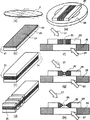
従来のTEM観察用試料の作製方法について、以下に説明する。図2に、従来のTEM観察用試料作製のための第1の方法を示す。図2中の(a)は、LSIを形成した半導体ウエハ(以下、単にウエハ又は基板と略記する)2を示しており、このウエハ2は、上層部2Aと、下層部(基板部)2Bとからなっている。いま、このウエハ2上の特定領域についてのTEM観察用試料を作製するものとする。先ず、TEM観察したい領域22に目印(図示せず)を付けて、この観察領域22を破壊しないようにして、ウエハ2にダイアモンドペン等で傷を付けて劈開するか、または、ダイシングソーを用いて切断して、短冊状のペレット21を切り出す(図2の(b))。次に、作製するTEM試料の中央部が観察領域22となるようにするために、観察領域22同士が向かい合うようにして接着剤23で貼り合わせ、貼り合わせ試料24を作る(図2の(c))。次に、この貼り合わせ試料24をダイヤモンドカッタでスライスし、スライス試料25を切り出す(図2の(d))。このスライス試料25の大きさは、3mm×3mm×0.5mm程度である。さらに、このスライス試料25を研磨盤上で研磨材を用いて薄く研磨して、厚さ20μm程度の研磨試料25'を作製し、これをTEMステージ上に搭載される単孔メッシュ28上に貼り付ける(図2の(e))。次に、この研磨試料25'の両面にイオンビーム27を照射して(図2の(f))、試料中央部のスパッタ(イオンミリング)加工を行い(図2の(g))、試料中央部に貫通穴が開いたらイオンビーム27の照射を止める(図2の(h))。このようにして厚さが100nm程度以下と薄くなった薄片部26をTEMにより観察していた。この方法については、例えば、高分解能電子顕微鏡−原理と利用法−(堀内繁雄著、共立出版社)の第182頁(公知文献1)に記載されている。
図3に従来のTEM試料作製のための第2の方法を示す。この方法は集束イオンビーム(以下、FIBと略記する)を利用して試料を作製する方法である。先ず、ウエハ2の観察すべき領域22の近傍にレーザ光またはFIBで目印(図示せず)を付けて、図3の(a)に示すようにウエハ2をダイシングして短冊状ペレット21を切り出し(図3の(b))、次に、このペレット21をスライスしてスライス試料21'を切り出す(図3の(c))。このスライス試料21'の大きさは、おおよそ3mm×0.1mm×0.5mm(ウエハの厚み)である。さらに、このスライス試料21'を研磨により薄片化し、この薄片化試料21"を切欠き部31'を持つ薄い金属円板からなるTEM試料ホルダ31に貼り付ける(図3の(d))。次に、この薄片化試料21"中の観察領域22を厚さ100nm程度の薄片部22'のみが残るようにFIB32を用いて薄片化して(図3の(e),(f))、これをTEM観察用試料とする。この方法に関しては、例えば、論文集:Microscopy of Semiconducting Materials 1989,Institute of Physics Series No.100,pp.501−506(公知文献2)に開示されている。
図4に従来のTEM試料作製のための第3の方法を示す。この方法については、特開平5−52721号公報(公知文献3)に開示されている。先ず、試料基板2の表面に対しFIB32が垂直に照射されるように試料2の姿勢を保ち、試料2上でFIB32を矩形形状に走査させ、試料2表面に所要の深さの矩形穴33を形成する(図4の(a))。次に、試料2表面に対しFIB32の軸が約20゜の傾きとなるよう試料2を70゜傾斜させ、矩形穴33の側壁に分離用の溝34を形成する(図4の(b))。試料2の傾斜角の変更は試料ステージ(図示せず)によって行われる。次に、試料2表面に対しFIB32が再び垂直となるよう試料2の姿勢を戻して、切り欠き溝35を形成する(図4の(c))。次に、プローブ36を保持するマニピュレータ(図示せず)を駆動してプローブ36先端部を試料2の分離すべき部分40の表面に接触させる(図4の(d))。この状態でガスノズル37から堆積性のガス39を供給しながら、プローブ36先端部を含む局所領域にFIB32を照射し、イオンビームアシストデポジション膜(以下、IBAD膜またはデポ膜と略記する)38を形成する。これにより、接触状態であった試料2の分離部分40とプローブ36先端部とがデポ膜38を介して固定接続される(図4の(e))。次に、試料2の分離すべき部分40の周囲の残りの部分をFIB32で切り欠き加工して、試料2から分離部分40を切り離す(図4の(f))。切り離された分離部分40はプローブ36先端部に固定保持された状態となる(図4の(g))。この分離部分40の観察所望領域を厚さ100nm程度以下にFIBを用いて薄片化して、それをTEM観察用の試料とする。
上記した第1,第2の従来方法においては、研磨や機械加工、TEM試料ホルダへの試料の貼り付け等試料作製者の熟練を要する手作業に頼らざるを得なかった。また、これらの従来方法では、所望の試料を作製するには、元のウエハやデバイスチップ等の基板を劈開や切断により分断せざるを得ず、所望領域の試料を取得するためには、その隣接部分の劈開や切断も余儀なくされる。一度観察や分析を行った後に、さらに別の箇所の観察や分析の必要が生じた場合には、試料基板が先の試料作製のために分断されてしまっているので、後の観察(分析)領域が破損や損傷を受けてしまっていたり、観察(分析)領域相互間の位置関係が判らなくなってしまっていたりして、正確な観察(分析)情報が継続して得られないと云う問題を有する。また、上記したイオンミリングやFIBによる薄膜化加工は、直接的に人手を要することはないが、加工時間が長いと云う難点がある。
また、最近ではウエハ径が300mmへと大口径化する傾向にあるため、ウエハ1枚に搭載されるデバイスチップの数が多いこと,デバイスそのものの付加価値が高いこと等のため、1箇所の観察や分析のために1枚のウエハを切断や劈開で分離してしまい、観察/分析対象領域以外を廃棄処分してしまうことは非常に不経済である。また、種々の顕微鏡を駆使してウエハ全体にわたって検査を行なった結果、ある領域に微小塵埃や異常形状が発見された場合、ウエハを各チップ毎に分割する前に、特に微小塵埃が無くなってしまう前に観察/分析を行なって原因を究明しなければ、最終的なデバイス製品に不良品が多発してさらに大きな損害をもたらす。ウエハを分割することなく、かつ複数のサンプルを短時間で作製できれば、非常に経済的であると共に、製品製造歩留まりの向上に大きく貢献する。
また、上記第3の従来方法では、試料を試料ステージに一度セットすれば、微小試料片の分離まで人間が直接手作業を行なう必要はないし、ウエハを不用意に切断する必要もない。しかし、この手法では、分離された試料片はプローブ先端に支持されたままの状態であるため、そのままで観察装置や分析装置内に導入して観察や分析を行っても、試料片が振動してしまい、信頼性ある観察,分析結果を得ることができないと云う問題点がある。
また、従来のTEM用試料ホルダとしては、図7に示すような単孔型ホルダ78(同図の(a)),切り欠き型ホルダ80(同図の(b)),およびメッシュ型ホルダ109(同図の(c))が知られている。上述した従来の第3の試料作製方法では、試料片40の大きさが20〜30μmと小さい場合、単孔型ホルダ78や切り欠き型ホルダ80では、単孔部79や切り欠き部108の内側壁への試料片40の取付けを正確に位置合わせして行なう必要があり、この取付け作業が容易でない。その点、メッシュ型ホルダ109では、試料片40の大きさに合わせた網目間隔のものを用いれば、試料片取付け位置そのものはある程度任意に選定することができる。しかし、このメッシュ型ホルダ109の場合には、図7の(d)に示すように、観察領域81に対応する電子線経路82がメッシュ構成部材109'により遮断されてしまって、TEM観察ができなくなってしまう場合がある。
発明の開示
従って、本発明の目的は、上述したような従来方法における諸問題を解消できるよう改良された試料作製方法、およびその方法を実施するのに使用して好適な試料作製装置を提供することである。
すなわち、本発明の第1の目的は、研磨やダイシング等の熟練の要る手作業を要さず、かつ、半導体ウエハや集積回路チップを劈開や切断等により分断してしまうことなくして、TEM等の観察装置や計測/分析装置内に導入して観察又は計測/分析する必要のある微小領域についての試料を作製することのできる試料作製方法を提供することである。
本発明の第2の目的は、上記した本発明の試料作製方法を実施するために用いるのに好適な試料作製装置を提供することである。
本発明の第3の目的は、摘出された微小試料片の取付けが容易なTEM用の試料ホルダを提供することである。
上記した第1の目的を達成するため、本発明の試料作製方法においては、試料台上に保持された集積回路チップや半導体ウエハ等の試料基板上の観察や計測/分析を所望する領域(以下、観察領域と云う)の近傍部にプローブ先端部を固定接続し、この観察領域近傍部の周辺にイオンビームを照射して、イオンビームスパッタ加工により上記観察領域を含んだ試料片を上記試料基板から分離摘出し、この分離摘出された試料片が上記プローブ先端部に固定接続されたままの状態で、上記プローブあるいは上記試料台を移動させることにより、上記した所望の観察や計測/分析を行なう装置用の試料ホルダまで搬送して、上記試料片を上記試料ホルダに固定接続し、しかる後に、上記プローブ先端部を上記試料片から切り離した上で、上記した所望の観察や計測/分析(以下、観察と云う)を行なうようにしている。
また、試料基板上の特定の観察領域の観察を行うためには、上記プローブ先端部を上記特定観察領域近傍部に固定接続する前に、上記特定観察領域を明示するためのマーキングを行っておき、上記プローブ先端部から上記試料片を切り離した後に上記のマーキングにより明示された上記特定観察領域に上記FIBを照射して薄膜化等の追加工を行う。
なお、上記プローブ先端部を上記試料基板の観察領域近傍部に固定接続する工程では、イオンビームアシストデポジション膜またはイオンビームスパッタ粒子再付着膜を介して両者間の接続を行うか、あるいは、融着法または金属接合法を用いて両者間の接続を行うことができる。
また、上記プローブ先端部を上記試料片から切り離す工程においては、イオンビームスパッタ加工法を用いることができる。あるいは、上記プローブ先端部を上記試料片に固定接続する方法として粘着剤を用いる方法を採用することもでき、その場合には、上記プローブ先端部を上記試料片から切り離す工程では、紫外線照射法または加熱法を用いることができる。また、上記プローブ先端部に上記試料片を固定接続する方法として靜電吸着法を用いることもできる。
また、上記第2の目的を達成するための本発明による試料作製装置は、試料基板を載置するための可動の試料台と、上記試料基板の所望の観察領域の近傍にプローブを接続するためのプローブ接続手段と、上記観察領域の周囲にイオンビームを照射して上記観察領域を含んだ試料片を上記プローブと接続された状態で上記試料基板から分離するための試料分離手段と、上記試料基板から分離された上記試料片を試料ホルダに固定保持するための試料片固定手段と、上記プローブを上記試料ホルダに固定保持された上記試料片から分離するためのプローブ分離手段とを含んで構成され得る。
上記試料台は、上記試料基板を載置し、かつ上記試料ホルダ(あるいは観察装置の試料ステージに着脱可能なホルダカートリッジ)を保持するための試料カセットと、上記試料カセットを保持するための可動の試料カセットホルダとを含んで構成され得る。
上記プローブは、ばね効果を有するものとすることができる。
上記プローブ接続手段は、上記試料基板の表面に上記プローブを接触させるためのプローブ接触手段と、上記プローブと上記試料基板表面との接触部にイオンビームアシストデポジション膜(IBAD膜)を形成させるためのデポ膜形成手段とにより構成することができる。上記プローブ接触手段は、上記プローブを保持して、該プローブを上記試料基板表面に対して相対移動させ得るマニピュレータ機構とすることができる。また、上記デポ膜形成手段は、上記プローブと試料基板表面との接触部にイオンビームを照射するためのイオンビーム照射光学系と、このイオンビーム照射部にアシストガスを供給するガス供給手段とより構成することができる。上記のデポ膜形成手段により形成された上記IBAD膜を介して、上記プローブが上記試料基板表面に固定接続される。
上記試料分離手段は、上記試料基板にイオンビームを照射するためのイオンビーム照射光学系を含んで構成される。該イオンビーム照射光学系は、イオン源と該イオン源からのイオンを成形イオンビーム(PJIB)として上記試料基板上に投射する投射光学系とからなるPJIB照射光学系、または、イオン源と該イオン源からのイオンを集束イオンビーム(FIB)として上記試料基板上に照射する集束光学系とからなるFIB照射光学系であることができる。また、上記イオンビーム照射光学系として上記PJIB照射光学系と上記FIB照射光学系とを併用することもできる。上記イオンビーム照射光学系を用いての上記試料基板上へのイオンビーム(PJIBまたはFIB)の照射により、該試料基板がスパッタ加工されて、上記試料片の分離摘出が行われる。また、上記試料分離手段は、上記試料基板上に第1の方向からイオンビームを照射するための第1のイオンビーム照射光学系と、上記試料基板上に上記第1の方向と異なる第2の方向からイオンビームを照射するための第2のイオンビーム照射光学系とを含んで構成されることができる。このように、2系統のイオンビーム照射光学系を備えることにより試料基板からの試料片の摘出加工がより容易となる。なお、上記試料分離手段として、レーザビーム照射光学系を用いてもよく、さらにはまた、イオンビーム照射光学系とレーザビーム照射光学系とを併用してもよい。
上記試料片固定手段は、上記試料ホルダの試料片保持部に上記試料片を接触させるための試料片接触手段と、上記試料片と上記試料片保持部との接触部にイオンビームアシストデポジション膜(IBAD膜)を形成させるためのデポ膜形成手段とより構成することができる。上記デポ膜形成手段は、先のプローブ接続手段におけるデポ膜形成手段と同様な構成とすることができる。このデポ膜形成手段により形成された上記IBAD膜を介して上記試料片が上記試料ホルダの上記試料片保持部に固定接続される。また、上記プローブ分離手段は、上記試料片を上記試料片保持部に固定接続しているIBAD膜にイオンビームを照射する手段であることができる。このイオンビーム照射により上記IBAD膜がスパッタ加工(除去)されて、上記プローブが上記試料片から分離される。
なお、上記プローブ接続手段および上記試料片固定手段は、上記したIBAD膜を利用するものに代え、イオンビームスパッタ粒子再付着膜を利用するものとしてもよく、さらには、融着法または金属接合法によるものとすることもできる。この場合、上記プローブ分離手段としては、イオンビームスパッタ加工法を用いることができる。また、上記プローブ接続手段および上記試料片固定手段としては、上記の他、粘着法によるものであってもよく、静電吸着法によるものであってもよい。
本発明による試料作製装置は、さらに、上記試料基板表面,上記プローブ先端部または上記試料ホルダ近傍を観察するための観察装置を含むことができる。該観察装置は、上記観察部位に電子ビームを照射するための電子ビーム照射光学系と、この電子ビーム照射によって上記観察部位から放出される2次電子を検出するための2次電子検出器と、該2次電子検出器の検出信号を用いて上記観察部位の2次電子像を表示させるための表示装置とで構成されることができる。また、上記の観察装置として、光学顕微鏡等の光学的な観察装置を用いることもできる。この観察装置を用いて、上記観察部位を観察することにより、上記プローブと上記試料基板との接触/接続状態,上記試料基板からの上記試料片の分離状態,さらには上記試料片と上記試料ホルダとの接触/接続状態等を適確に把握することが可能となる。
また、本発明による試料作製装置は、さらに、上記プローブと試料基板間,上記試料片と試料基板間,および上記試料片と上記試料ホルダ間の接触/接続状態および分離状態を検知するための検知手段を備えることができる。該検知手段は、それぞれ対応する部材間の接触抵抗の変化を利用したものであってもよく、あるいは、上記した2次電子像上における電位コントラストの変化を利用したものであってもよい。この検知手段によって、上記したそれぞれ対応する部材間の接触/接続状態および分離状態をより正確に把握することができる。
上記試料ホルダは、特に、試料片を保持するための金属細線と、該金属細線の両端部を固定支持するための支持部とで構成することができる。かかる試料ホルダ構成において、上記金属細線に上記試料片を固定保持させることにより、TEM観察に適した試料保持系が得られる。
本発明の上記以外の目的,構成,並びにそれによって得られる作用効果については、以下の実施例を挙げての詳細な説明の中で順次明らかにされよう。
【図面の簡単な説明】
図1は、本発明の一実施例になる試料作製装置の基本構成を示す図,
図2は、従来のTEM観察用試料作製方法の一例を示す工程説明図,
図3は、従来のTEM観察用試料作製方法の他の一例を示す工程説明図,
図4は、従来のTEM観察用試料作製方法のさらに他の一例を示す工程説明図,
図5A,図5Bおよび図5Cは、本発明による試料作製装置において用いられるイオンビーム照射光学系の構成例を示す要部構成図,
図6A,図6B及び図6Cは、本発明による試料作製装置において用いられるプローブ駆動装置の構成例を示す図,
図7は、従来のTEMホルダの構成例を示す図,
図8A,図8B,図8C及び図8Dは、本発明による試料作製装置において用いられる金属細線型TEMホルダの構成例を示す図,
図9Aおよび図9Bは、本発明による試料作製装置において用いられるTEMホルダの試料カセット上への載置方法の一例を示す図,
図10は、本発明による試料作製装置において用いられるTEMホルダカートリッジの試料カセット上への載置方法の一例を示す図,
図11は、本発明による試料作製装置において用いられるばね効果を有するプローブの一構成例およびその機能を説明するための図,
図12は、本発明による試料作製装置におけるプローブの加熱方法の一例を示す図,
図13は、本発明による試料作製装置におけるプローブと試料片との間の静電吸着法による結合方法の一例を示す図,
図14は、本発明による試料作製装置におけるTEMホルダの加熱方法の一例を示す図,
図15は、本発明による試料作製装置の別の一構成例を示す図,
図16は、本発明による試料作製装置の更に別の一構成例における試料片の分離方法の一例を示す図,
図17は、本発明によるTEM試料作製方法の別の一実施例の工程説明図,
図18は、本発明によるTEM試料作製方法のさらに別の一実施例の部分工程説明図,
図19は、本発明のさらに別の実施例になる試料作製装置の基本構成を示す図,
図20A,図20B,図20Cは、本発明による試料作製装置において用いられる試料移送装置の別の構成例を示す図,
図21は、本発明による試料作製装置において用いられる試料移送装置の設置位置に関する説明図,
図22は、本発明による試料作製装置における試料ホルダの設置方式の一例を示す図,
図23は、本発明による試料作製装置における試料ホルダの設置方式の別の一例を示す図,
図24は、本発明による試料作製装置における試料ホルダの設置方式のさらに別の一例を示す図,
図25は、本発明による試料作製装置における試料ホルダの設置方式のさらに別の一例を示す図,
図26は、本発明による試料作製装置における試料ホルダの形態についての説明図,
図27は、本発明のさらに別の一実施例になる試料作製方法の工程説明図,
図28は、本発明による試料作製装置において用いられる試料移送装置のさらに別の構成例を示す図,
図29は、図28に示した試料移送装置を用いてプローブ先端部を試料基板表面へ接触させる手順を示す図,
図30は、図29に示したプローブ先端部を試料基板表面へ接触させる手順を説明するためのフローチャート図,
である。
発明を実施するための最良の形態
以下、本発明の実施の形態について、実施例を挙げ、図面を参照して詳細に説明する。
<実施例1>
図1に、本発明による試料作製方法を実施するために用いられる試料作製装置の一実施例の基本構成を示す。
本実施例になる試料作製装置は、試料(観察対象)である半導体ウエハや半導体チップ等の基板2にイオンビーム13を照射するイオンビーム照射光学系1,基板2を載置して移動させる試料台3,基板2の観察しようとする箇所(観察領域)を特定するために試料台3の位置を制御する試料台位置制御装置3',プローブ11を保持して移動させるプローブ駆動装置4,プローブ駆動装置4を制御するプローブ駆動制御装置4',基板2の上記観察領域近傍に堆積性ガス(デポガス)を供給するためのデポガス供給源8,デポガス供給源8を制御するデポガス供給制御装置8',基板2表面に電子ビーム16を照射するための電子ビーム照射光学系9,および、基板2表面から放出される2次電子を検出する2次電子検出器12を含んで構成されている。なお、イオンビーム照射光学系1,試料台3,プローブ駆動装置4,デポガス供給源8,電子ビーム照射光学系9,および2次電子検出器12は、高真空排気される真空室77内に配置されていることは云うまでもない。
試料台3は、基板2を載置するための試料カセット17とこの試料カセットを固定保持するためのカセットホルダ18とから構成されている。また、試料台3上には基板2から分離された試料片を保持してTEM等の観察/分析装置(図示せず)内に導入するための試料片ホルダ(以下TEMホルダと云う)19を保持するためのホルダ保持具20が設けられている。試料台3は、試料台位置制御装置3'によって駆動制御され、基板2の3次元方向位置および基板2表面のイオンビーム軸に対する傾き角並びに回転方向角度を任意に設定できる。これによって、基板2表面上でのイオンビーム照射位置(加工位置)および基板2表面に対するイオンビームの照射角度並びに回転方向角度を任意に設定できる。
イオンビーム照射光学系1は、基板2の上記観察領域の周囲にイオンビーム13を照射して、イオンビームスパッタ加工法によって上記観察領域を含む試料片を分離する(切り出す)ために用いられる。また、イオンビーム13は、上記観察領域近傍の基板2表面にイオンビームアシストデポジション法(以下、IBAD法と略記する)によってプローブ11の先端部を固定接続する細のアシストイオンビームとして、および、基板2から分離された試料片をTEMホルダ19にIBAD法により固定接続する際のアシストイオンビームとして、さらには、TEMホルダ19に固定接続された試料片からプローブ11の先端部をイオンビームスパッタ加工法により分離する(切り離す)際の加工用イオンビームとしても用いられる。イオンビーム照射光学系1は、イオンビーム駆動装置7によって駆動制御される。
プローブ駆動装置4は、プローブ11先端部を基板2の観察領域近傍に接触させたり、基板2から分離された試料片をプローブ11先端部に固定接続してTEMホルダ19まで搬送したりするための、いわゆるマニュピュレータである。プローブ駆動装置4は、プローブ駆動制御装置4'により駆動制御される。
デポガス供給源8は、基板2の上記観察領域近傍にデポガスを供給してIBAD法によりデポ膜を形成し、このデポ膜を介してプローブ11先端部を基板2表面に固定接続するために用いられる。また、このデポガスは基板2から分離された試料片をTEMホルダ19にIBAD法により固定接続する際にも用いられる。上記のデポガスとしては、例えばヘキサカルボニルタングステン[W(CO)6]を用いることができ、このガスを固定接続すべき部分間(プローブ11先端部と試料片との間または試料片とTEMホルダ19との間)に供給しながら、そこにイオンビーム13を照射することにより、タングステン膜(W膜)が形成され、このW膜により接続すべき部分同士間が固定接続される。なお、W膜によって固定接続されたプローブ11先端部と試料片とを分離するには、両者を接続しているW膜部分にイオンビームを照射し、イオンビームスパッタ法(以下、IBS法と略記する)によって上記W膜部分を除去して、両者間の分離を行なう。デポガス供給源8は、デポガス供給制御装置8'によって駆動制御される。
電子ビーム照射光学系9及び2次電子検出器12は、基板2表面を走査2次電子顕微法により観察するための観察装置を構成しており、該観察装置は、電子ビーム源14からの電子ビーム16を偏向レンズ15により走査しながら基板2表面に照射して、基板2表面から放出される2次電子を2次電子検出器12で検出し、表示装置(CRT)5に基板表面の走査2次電子像(SEM像)を表示させる。なお、この観察装置は、プローブ11先端部近傍やTEMホルダ近傍を観察するためにも用いられる。これにより、観察領域の表面状態の確認,試料片の基板2からの分離状態の確認,プローブ先端部の基板2表面への接触状態の確認,試料片のTEMホルダ19への接触状態の確認等ができる。なお、試料片の基板2からの分離状態の確認は、上記SEM像の電位コントラストの変化を検知することによっても行なうことができる。また、上記接触状態の確認および分離状態の確認はプローブ11と試料台3との間の電気抵抗(接触抵抗)の変化を検知して行なうようにしてもよい。電子ビーム照射光学系9は電子ビーム駆動装置10によって駆動制御される。
なお、基板2から摘出される試料片の大きさは、10μm角〜100μm角程度であるので、光学顕微鏡を表面観察手段として用いるようにしてもよい。
なお、試料台位置制御装置3',プローブ駆動制御装置4',イオンビーム駆動装置7,デポガス供給制御装置8',電子ビーム駆動装置10,および表示装置5は、中央処理装置(CPU)6によって統括制御される。
以下、上記試料作製装置の各部の具体的な構成、並びに、本装置を用いての試料作製方法の各工程について詳述する。
[イオンビーム照射光学系]
図5Aは、成形イオンビーム(PJIB)の照射光学系1の要部構成図であり、イオン源41から放出されたイオンビームをビーム制限アパーチャ42,照射レンズ43によりマスク板44に照射し、マスク板44のパターン開口45を通過したイオンビームを投射レンズ46によって試料台3上に載置された基板2表面に投射する。こうして形成されたPJIB13により、基板2表面をパターン開口45とほぼ相似形に加工する。PJIBの場合には、イオン源41直後のイオンビームの拡がりは直接収差には影響しないため、アパーチャ42によるイオンビーム制限角を大きく採ることができるので、イオンビーム電流量を大きく取ることができる。このため、加工速度が大きいという特長を持つ。
また、図5Bに示すように、マスク板44に設ける開口パターン45を光軸47が通過する辺48を有する矩形状パターンとすることにより、辺48に対応するPJIBの辺のボケが極めて小さくなり、このPJIBを投射し続けて形成される基板2の凹部の対応辺の分解能を高くできる。従って、辺48に対応する加工面は、基板2表面に対して垂直な断面となる。このように、光軸47を通過する辺48を有する矩形状開口パターンを駆使することで、垂直に切り立った壁面構造を形成することができる。これについては特開平7−317745号公報『イオンビーム加工方法及び装置』にも開示されている。
図5Cは、基板加工に集束イオンビームを用いる集束イオンビーム(FIB)照射光学系1の要部構成を示す。イオン源41から放出されたイオンビームをビーム制限アパーチャ42'、イオンビームの拡がりを抑制したり集束させたりする集束レンズ49,イオンビームを基板2上に集束させる対物レンズ50を通すことで集束イオンビーム52を形成する。この集束イオンビーム52を偏向器51を用いて基板2上で走査することにより、走査形状に合わせて基板2を加工する。このように集束イオンビーム(FIB)を用いる場合は、精密な加工が可能であり、また、基板2表面等の観察手段としても兼用できる。ただし、精密加工のために集束イオンビームの集束性を高く保つためには、色収差や球面収差を抑えるためにビーム制限アパーチャ42'によりイオンビームの開口角を制限しなければならない。このため、ビーム電流量を大きく取ることは難しく、加工速度があまり大きくならないという欠点がある。なお、加工速度を増すには、基板表面に反応性ガスを供給しながらスパッタを行なう集束イオンビームアシストエッチング法等の手法を用いてもよい。集束イオンビームを観察手段としても用いるには、集束イオンビーム52によって基板2表面を走査し、基板2表面からの2次電子53を2次電子検出器12で検出して、画像化表示させればよい。
上述したように、試料加工用イオンビームとして、PJIBを用いると高速加工が実現でき、FIBを用いると精密加工の実現及び観察手段としての兼用ができるという利点がある。
[プローブ駆動装置]
図6A,図6B,図6Cは、それぞれプローブ駆動装置4の一構成例を示す図である。プローブ駆動装置4は、真空室77の側壁54に設けられた開口62を通して外から挿入する構造である。この構造により、プローブ11を試料台3とは独立に移動させることができ、基板2とTEMホルダ19とへのプローブ11の移動が容易になる。
プローブ駆動装置4は、図6Aに示すように粗動部56と微動部55との2部分から構成される。粗動部56による粗動軸65のX軸方向の粗動は、調整ネジ57により軸59を押した時のバネ60の伸縮によって行われる。Z軸方向の粗動は、調整ネジ58で軸59を押した時の支点63を中心としたてこの原理で稼働する。Y軸方向の調整ネジは図示されていないが、紙面手前側に存在し、Z軸方向と同様の原理で稼働する。バネ60,61は軸59を調整ねじ57,58の先端部にそれぞれ押しつけるためのものであり、Y軸用のバネ(図示せず)もZ軸用のバネ同様に設けられている。粗動部56の位置精度は、以下に説明するように、微動部55のストロークよりも小さい値を持つものとする。微動部55は、できるだけコンパクトであることが要求されるため、圧電素子を用いて構成されている。特に、本実施例では、バイモルフ圧電素子を用いている。バイモルフ圧電素子には、他の圧電素子に比べ、比較的大きな移動範囲(数100μm以上)を持つ利点がある。このため、粗動部56に高い位置精度を要求する必要が無いので、粗動部の製作が容易となる。また、プローブ11先端部の位置制御はμmのオーダであればよいので、圧電素子の中では比較的分解能が悪いバイモルフ圧電素子でも十分に対応できる。
図6Bに、3軸バイモルフ圧電素子を用いた微動部55の具体的構成例を示す。微動部55は、それぞれX,Y,Z方向微動を受け持つバイモルフ圧電素子66,67,68を有している。プローブホルダ70は、プローブ11を3軸方向微動部(バイモルフ圧電素子68の移動端)に固定するためのものである。また、バイモルフ圧電素子67の固定端は、微動部固定治具69を介して粗動軸65に固定接続されている。バイモルフ圧電素子の駆動には特殊な回路を要することなく、単純な電圧印加によって行なうことができる。このようにバイモルフ圧電素子を利用することにより、コンパクトで、大きなストロークを有する微動部をより経済的に構成できる。微動部55をコンパクトに作成する必要があるのは、以下のような理由による。
基板2の加工に図5Cで説明した集束イオンビーム(FIB)52を用いる場合は、対物レンズ50から基板2までの距離が短いほど、より加工精度を上げることができる。また、基板加工に図5Aで説明した成形イオンビーム(PJIB)を用いる場合は、開口パターン45の投射倍率を大きく取るために、PJIB照射光学系の投射レンズ46と基板2との間に距離が小さいほど良い。すなわち、上記したどちらのビームを用いる場合にも、基板2と最終段レンズとの間の距離が小さい方が望ましい。このため、基板2と最終段レンズとの間およびその周囲空間が体積的に制限される。基板2の周囲には、観察手段,2次電子検出器12,デポガス供給用ノズル8や、さらに、場合によっては、アシストエッチング用ガスの供給ノズル等が配置されるので、これらと場所的に干渉しないためには、プローブ駆動装置4の先端部分(微動部55)は、できるだけコンパクトに構成されていなければならない。
図4に示した従来技術においては、基板から分離した試料片を搬送するマニピュレータは3軸バイモルフ圧電素子で構成されているが、このマニピュレータの設置位置が明らかにされていない。ただ、その出典公報中の図3からは、このマニピュレータは、ステージ上に設置されているものと読み取れる。このように、マニピュレータが試料台上に設置されているために、観察対象領域がウエハの中心部にある場合には、マニピュレータ設置位置から観察対象領域までの距離がマニピュレータの移動ストロークよりも遥かに大きくなるため、このようなステージ上に設置されたマニピュレータでは、観察対象領域まで届かないと云う致命的な問題点を有することになる。
一方、図6Aに示したプローブ駆動装置4は、試料台3とは分離して設けられており、観察対象領域が大きな試料(ウエハ)の中央部であっても、問題なくそこにアクセスすることができる。また、プローブ11の不使用時には粗動部56により微動部55およびプローブ11を大きく移動させて退避させることができるため、他の構成部品の邪魔になることはない。
プローブ駆動装置4の他の一構成例を図6Cに示す。本例では、粗動機能と微動機能とを兼備した第1のプローブ駆動機構76を試料台3から十分に離れた位置に設置し、その移動端側に延長棒71を介して、Z方向微動機能のみを持った第2のプローブ駆動機構(バイモルフ圧電素子)72を取り付けて、その移動端側にプローブ11を固定保持させてある。本構成には、図6Bの構成に比較して以下のような利点がある。すなわち、図6Bの構成では、X,Y,Zの3軸方向共バイモルフ圧電素子で微動させているが、バイモルフ圧電素子は一端を支点にして他端が撓む動きをするため、他端は印加電圧に従って円弧状軌道を描く。つまり、XY平面内の移動では、1個のバイモルフ圧電素子(例えば、X軸方向微動用圧電素子66)の動作のみでは、プローブ11先端部が対応する軸方向(X軸方向)に直線的には移動しない(すなわち正確にX軸方向に移動しない)。従って、3個のバイモルフ圧電素子66,67および68で微動部55を形成すると、プローブ11先端部を所望位置に正確に移動させるためには、これら3個のバイモルフ圧電素子を複雑に関連させて操作しなければならないと云う問題がある。この問題を解決するためには、正確に直線駆動が可能なプローブ駆動機構を用いればよいが、長いストローク(100μm〜数mm)と高い分解能(μmオーダ以下)を兼ね備えた構造となると、機構を複雑にする必要があり、バイモルフ圧電素子の場合と比較してサイズが大きくなる。このため、上述の理由から、試料台3回りの他の構成含品と場所的に干渉してしまうと云う問題が残る。
これに対し、図6Cでは、第1プローブ駆動機構76は、X軸方向駆動部73,Y軸方向駆動部74,およびZ軸方向駆動部75の移動ストロークがそれぞれ約5mm、移動分解能がそれぞれ0.1μmであり、粗動機能と微動機能とを兼備した構造としてある。上述したように、最終段レンズ46,50(図5A,図5C)と基板2との間にはその他種々の部品が混在配置されている。図6Cのプローブ駆動装置構成によれば、これら他部品との場所的な競合から解放され、容易に試料片を摘出,搬送することができる。
上述のようなプローブ駆動装置4を用いることで、プローブ11先端部を基板2表面上でサブミクロンオーダの分解能で位置決めすることができる。また、プローブ駆動装置4を試料台3上には設置せずに、プローブ11を試料台3とは独立して移動させることができるようにしているので、基板2およびTEMホルダ19へのプローブ11先端部のアクセスが容易になる。
プローブ11先端部の基板2への接触状態確認、試料片の基板2からの分離終了確認、試料片のTEMホルダ19への接触状態確認、さらに試料片とプローブ11との分離状態の確認は、2次電子検出器12の検出信号から得られる2次電子像の電位コントラストの変化を検知することによって確認する。また、プローブ11と試料台3との間の接触抵抗をモニタして、その変化を検知することにより確認するようにしてもよい。
[TEMホルダ]
図8A,図8B,図8C,および図8Dに、TEMホルダ19の具体的構成例を示す。図8Aに示すTEMホルダ19は、金属細線83が切欠き部83'を有するドーナツ状の固定部84に固定保持された構造を有する。この金属細線83の直径は10μmφ〜500μmφの範囲で、固定部84は一般的なTEM試料導入用のステージ(以下TEMステージと云う)に載置できる寸法であり、本構成例では、その外径を3mmφとした。以下に、この金属細線型TEMホルダ19の有効性について述べる。
試料片40を基板2から分離するためには、試料片40の底面と基板2との分離(以下底浚いと呼ぶ)が必要であるが、イオンビームによる底浚いでは、基板表面に対してイオンビームを斜め方向から入射させて加工を行なうため、試料片40の底面には底浚い時のビーム入射角と加工アスペクト比からなる傾斜が付いている。しかし、上記の金属細線型TEMホルダ19を用いれば、かかる底面傾斜を有する試料片40であっても、観察試料断面86を垂直に保ったままで金属細線に正しく接触させることができる(図8D)。例えば、面積10μm×30μmで深さ10μmの試料片40を切り出す場合は、試料台3を60゜傾けてイオンビームによる底浚い加工をすれば、観察所望領域86が陰にならないような金属細線8の径はほぼ40μm〜50μmφ程度になる。このように、金属細線型TEMホルダ19に試料片40を載置することにより、試料片40と金属細線83との接続部に自由度を持たせることができ、かつ観察所望領域86を通過した電子線82が金属細線83によって遮断されることがないようにすることができる(図8B)。
また、図8Cに示すような金属細線固定部85を有する金属細線型TEMホルダ19でも上記同様の効果が得られる。また、1本の金属細線83上に複数個の試料片40−1,40−2,40−3を固定することにより、TEM内に複数個の試料を同時に持ち込むことが可能になり、TEM観察の効率を向上させ得ると云う利点が得られる(図8D)。このように、金属細線型のTEMホルダを用いることで、微小な試料片の載置が容易になり、かつ、TEM観察用の電子線の経路が金属細線によって遮られることがないようにすることができる。
[試料カセットおよびTEMホルダ]
図9A,図9BにTEMホルダ19を試料カセット17上に載置するための構成例を示す。本例では、TEMホルダ19として、図8Aに示した金属細線型TEMホルダ19を使用している。図9Aは、試料カセット17の全体図およびその一部(点線の丸で囲んだ部分)の拡大図である。試料カセット17にTEMホルダ19載置用の溝を形成し、この溝の端面とホルダ保持具20とによりTEMホルダ19を挟んで固定する。この時に、TEMホルダ19の金属細線83の垂直方向位置を基板2表面位置と近くして、摘出試料片の保持位置を基板2表面高さとほぼ同じになるように設定すると、プローブ11を上下(Z方向)に大きく動かす必要がなくなるため高速アクセスを実現し易くなり、また試料片損傷の可能性をも減らすことができる。また、図9Bに示すように、試料カセット17上にTEMホルダ載置用の複数の溝20−1,20−2,20−3,20−4を設け、複数のTEMホルダ19−1,19−2,19−3,19−4を同時に載置できるようにしておけば、試料室の一度の真空引き操作で、同一基板2から複数個の試料片を切り出すことができ、試料作製効率をさらに高くできる。
図10に、TEMホルダ19を試料カセット17上に装着するための一構成例を示す。同図に示すように、TEMステージ87において、TEMホルダ19周辺をカートリッジ化しておき、このホルダカートリッジ88を複数個試料カセット17上に搭載する。こうすることで、真空容器外からTEMステージ87を挿入(サイズエントリー)し、所望のホルダカートリッジ88をそれに装着して、このTEMステージ87をそのままTEM試料室内に導入できる。このように、TEMステージ87のTEMホルダ周辺をカートリッジ化することで、TEMへの試料の装着が容易になる。
[プローブ]
図11に、プローブ11の一構成例を示す。ここでは、特に、ばね効果を有するプローブ構成例を示す。同図の(a)に示すように、細長いプローブ11の途中に、屈曲部からなるばね構造部89を設けてある。かかる構成により、プローブ11の先端部を基板表面の試料片形成部2−1に接触させた時に、同図の(b)に示すように、プローブ11先端部と試料片形成部2−1間にかかる衝撃力をばね構造部89が吸収するため、両者の損傷を防止することができる。また、試料片形成部2−1上にプローブ11先端部を接触させた後に、接触位置90とプローブホルダ91との相対位置が熱ドリフト等により微妙に変化したとしても、例えば、同図の(c)に示すように、ばね構造部89のばね効果によって両者の接触位置90を安定に保つことができる。
このように、ばね効果を有するプローブを用いれば、プローブ及び試料片の両方の損傷を抑制することができ、また、熱ドリフト等による両者間の相対位置変化をも補償できる。
[試料片形成部とプローブ先端部との固定及び分離手段]
試料片形成部とプローブ先端部との間の固定,分離方法として、先にIBAD法によるデポ膜形成技術,IBS法によるデポ膜除去技術をそれぞれ用いる例につき説明したが、それ以外にも、以下のような固定,分離方法を用いることができる。
すなわち、先のデポガスを用いるIBAD法に代え、基板2からのイオンビームスパッタ粒子の基板2上への再付着により形成される膜(以下、リデポ膜と云う)を介して固定接続する方法を用いることもできる。この場合の分離方法としては、上記のリデポ膜をIBS法により剥離する方法を用いることができる。あるいは、IBS法によってプローブを切断して分離するようにしてもよい。
また、プローブ11先端部表面に粘着材を付着させておき、該プローブ先端部を試料片形成部2−1に接触させるだけで両者間の固定接続ができるようにすることもできる。この方法は、先のIBAD法によるデポ膜を用いる場合と異なり、固定接続のための作業時間を低減し得る利点を有する。上記粘着材として紫外線照射により粘着力を減少させることができる紫外線剥離型粘着材を用いた場合には、紫外線照射手段を用いて、試料片40とプローブ11との分離を行なうことができる。ただし、この場合には粘着部に紫外光が照射できると云う条件が必要であり、紫外光が遮断されてしまうような条件下では使用できない。上記の固定用粘着材として加熱により粘着力を減少させることができる加熱剥離型粘着材を用いた場合には、加熱手段を用いて、試料片40とプローブ11との分離を行なうことができる。例えば、図12に示すように、プローブ11近傍に通電ライン92を設け、通電加熱によりプローブ11を80〜100℃程度に加熱することにより、上記の加熱剥離型粘着材を容易に剥離させ得る。
図13にさらに他の固定接続方法を示す。本方法は、試料加工方法としてイオンビーム(正イオンビーム)13によるIBS法を用いる場合において、静電吸着法により試料,プローブ間の固定及び分離を行なうものである。プローブ11の表面を絶縁物93で構成し、プローブ11と試料片形成部2−1との間に電位差を与えることにより、静電吸着力によって両者間の固定接続を行なう。本方法は、化学的変質や汚染を伴わないという利点を持つ。ここで、試料片形成部2−1側が正電荷を持つようにしている(図13の(a))理由は、照射される正イオンビーム13によって中和されることがないようにするためである。負イオンビームや電子ビームを照射する場合には試料側を負に帯電させておけばよい。こうして、図13の(b)のように、試料片40とプローブ11先端部間の固定接続ができる。このプローブ11先端部に固定接続された試料片40をTEMホルダへと搬送して金属細線83の固定(固定法については後述する)した後に、図13の(c)のように、プローブ11と金属細線83間を短絡して上記の帯電電荷を中和することで、図13の(d)のように、プローブ11先端部を試料片40から分離することができる。
また、その他にも、プローブ11を通電加熱法(図12と同様な方法)や局所的なレーザー照射による加熱法等で高温化し、試料片形成部2−1と接触部を熱的に反応させて融着による固定を行なうこともできる。ただし、試料片形成部2−1全体の高温加熱は、試料片自体を変質させる可能性があるので、短時間で局所的な加熱を行なう必要がある。
また、清浄な表面を有する金属同士は、両者を接触させただけで接合することも良く知られている。このため、例えば、真空中で、試料片形成部2−1の固定部と金属(例えばタングステン)製のプローブ11先端部とに、それぞれイオンビーム照射による表面スパッタを施してそれぞれの表面を清浄化した後に、両表面を接触させれば、金属接合によって両者間の固定接続ができる。また、この表面清浄化による接合は、シリコン同士でも可能であるため、試料がシリコンの場合には、プローブ材にもシリコンを用いることにより、上記と同様にして、両者間の固定接続ができる。
[試料片とTEMホルダとの固定手段]
図14に、試料片40のTEMホルダ19への固定方法の他の一例を示す。本例では、TEMホルダ19と試料片40との接触部を加熱することにより、両者間の固定接続を行なっている。TEMホルダ19の金属細線83の固定部84を2部分に分け、両部分間に絶縁部94を配置して、ホルダ支持用電極95,96間に電流を流すことで、通電加熱によって金属細線83を高温化する。高温化した金属細線83に試料片40の固定部位を接触させることにより、融着によって両者間の固定接続ができる。
試料片40のTEMホルダ19への固定には、この他に、前述したIBAD法によるデポ膜を用いる固定方法やIBS法によるリデポ膜を用いる固定方法を用いてもよい。また、粘着材を用いて試料片40とTEMホルダ19とを固定する場合には、前述したプローブ11と試料片40との固定の場合のような一時的な固定とは異なって、長時間(少なくともTEM観察が終了するまで)の安定した固定が要求されるため、持続力を持った粘着材を使用することが望ましい。
さらに他の固定方法として、TEMホルダ19と試料片40との固定部における双方の表面を清浄化して、両清浄化表面を接触させることによって両者間の接合を得るようにしてもよい。この表面清浄化には、イオンスパッタ法等を用いることができる。
[イオンビーム加工による試料片の摘出]
試料片40を基板2から分離するためには、前述した底浚い加工の技術が必要である。この底浚い加工には、次の4つの方法がある。
第1の方法は、図1で示したように、加工用ビームとして1つのPJIB光学系からのイオンビーム(PJIB)のみを用いる方法であり、試料台3を傾斜させて基板2表面に対し斜め方向からPJIBを照射することにより、所望の底浚い加工を行なう。この方法は、先に図4で説明した方法、または、後ほど図17において説明する方法と同じである。
第2の方法は、図5Cで示したように、加工用のイオンビームとして集束イオンビーム(FIB)を用いる方法であり、この場合にも、上記第1の方法と同様に、試料台3を傾斜させて、FIBを斜め方向から照射(走査)することにより、試料片摘出のための底浚い加工を行なう。
第3の方法は、図15に示すように、試料基板2表面に所要深さの垂直溝を形成するための第1のPJIB光学系(カラムI)1の他に、上記した底浚い加工専用の斜方向に設置した第2のPJIB光学系(カラムII)97を設けて、該カラムIIを用いて所望の底浚い加工を行なう。斜方向のカラムIIとして、PJIB光学系の代わりにFIB光学系を用いてもよい。
第4の方法は、図16に示すような、イオンビームを用いないで底浚い加工する方法である。基板2表面の観察所望領域の周囲に、イオンビーム加工で深溝98を形成して凸状の試料片形成部99を形成後、深溝98のうちの一辺側にテーパ部材100を挿入して、剪断により試料片40を分離する。この方法は、上述のイオンビームを用いる底浚い加工法と比較し、短時間で底浚い加工ができる特長がある。また、上記の剪断分離を容易にするため、図16の(b)に示すように、試料片形成部99の回りに形成する深溝98を少し傾斜させ、試料片形成部99がその下方に行く程細くなるようにしておくのもよい。また、図16の(c)に示すように、圧電素子101に取り付けられた微小板材102を深溝98内に挿入し、この圧電素子101の駆動によって試料片形成部99に横方向の力を加えて、試料片40を剪断分離するようにしてもよい。
上記した底浚い加工を行なうことで、基板2の上部の浅い領域だけの微小試料片を形成することができるため、加工時間が短くなる。特に、底浚い加工に上記した応力印加による剪断分離法を用いることにより、高速に試料片を分離摘出することができる。
<実施例2>
図17に本発明の他の一実施例になる試料作製方法の工程を示す。本実施例は、図1に示した試料作製装置を使用して、加工用イオンビームとしてPJIBのみを用いる例である。
始めに、基板2内の観察すべき領域103(図17の(a))の周囲に、コの字型の開口を持ったマスクを用いてPJIB13'を照射し(図17の(b))、コの字型断面形状の溝104を形成する(図17の(c))。次に、図1の試料台3を傾けて、PJIB13'により、底浚い加工を行う(図17の(d))。次に、プローブ駆動装置4に保持されたプローブ11の先端部を試料片形成部99に接触させる。両者の接触の状態は、プローブ11と基板2(すなわち試料片形成部99)との間の接触抵抗の変化や、2次電子像上での電位コントラストの変化等から検知する。接触させたプローブ11先端部と試料片形成部99とをIBAD法によるデポ膜を用いて固定接続する(図17の(e))。その後、残りの辺をPJIB13'で切断する(図17の(f))。この切断の完了は、プローブ11(即ち、試料片40)と基板2との間の接触抵抗の増大又は2次電子像の電位コントラストの変化等で検知する。このようにして、基板2から試料片40を切り出して、プローブ駆動装置4によりTEMホルダ19へと搬送する(図17の(g))。次に、この切り出された試料片40をTEMホルダ19の金属細線83に接触させる(図17の(h))。この時の接触状態の検知は、プローブ11(即ち、試料片40)とTEMホルダ19(即ち、金属細線83)との間の接触抵抗の減少または2次電子像上の電位コントラストの変化により行う。こうして、試料片40を金属細線83に接触させた後、IBAD法によるデポ膜を用いて両者間の固定接続を行う。試料片40を金属細線83に固定した後、プローブ11先端部と試料片40との接続部にPJIBまたはFIBを照射してスパッタ加工を行い、プローブ11先端部を試料片40から分離する(図17の(i))。この分離の完了は、プローブ11と金属細線83との間の接触抵抗の増大や2次電子像上での電位コントラストの変化等から検知する。最後に、試料片40に、再度PJIBまたはFIBを照射して最終的に観察すべき領域103を厚さ100nm以下程度に薄く仕上げ加工してTEM試料とする(図17の(j))。
本実施例では、TEM観察用試料の作製を例にとり説明したが、その他の観察,分析,計測用の試料の作製にも同様に用いることができることは云うまでもない。その場合、上記した観察領域を薄く仕上げるための加工工程(図17の(j)))は必ずしも必要ではない。
本発明による試料作製方法は、上記実施例に限定されるものではなく、前述した他の装置や技術手段と組み合わせるようにしてもよいことは云うまでもない。例えば、底浚い加工を行う工程(図17の(d))は、前述した4つの方法のいずれでもよく、プローブ11と試料片形成部99との固定方法やプローブ11の試料片40からの分離方法も前述した他の方法と置換してもよい。また、試料片形成に用いるPJIB13'も、上記実施例に示したコの字断面形状のものに限定されるものではなく、矩形パターンのPJIB投射を複数回組み合わせて同様の加工パターンを得るようにしてもよく、矩形パターンのPJIBを走査して所望の加工パターンを得るようにしても構わない。また、PJIBの代わりに、FIBを用いてもよい。また、試料作製装置にPJIB投射光学系とFIB照射光学系とを併設しておき、加工目的に応じPJIBとFIBとを使い分けるようにしてもよい。また、イオンビームスパッタ加工法とレーザビーム加工法とを併用して分離加工してもよい。
<実施例3>
図18に本発明による試料作製方法のさらに他の一実施例を示す。本実施例は、前述した試料作製方法において、基板2中の観察(分析)位置を明確化するためのマーキング工程をさらに付加したものである。なお、その他の工程は、図17に示した工程と実質的に同じであるのでここでは図示説明を省略する。本実施例では、観察位置を含む試料片40を摘出後に、観察位置(すなわち、TEM観察用の薄壁部を形成すべき位置)105が特定できなくなるのを防止するために、該観察位置を明示するためのマーキングを施す工程を付加する。基板2がまだウエハやチップの状態では、CADデータ等から位置割り出しが可能であり、試料片摘出加工前に観察位置(薄壁形成位置)105にマーキングを施しておく。このマーキングは、例えば観察位置105の両端に十字形のマーク106,107を集束イオンビーム加工等で施せばよい(図18の(a))。こうすることで、試料片40摘出後でも、観察位置を明確化することができる(図18の(b))。この2つの十字形マークを結び線上部分(観察対象部分)105を残して薄壁化することで、所望位置の断面観察が可能になる(図18の(c))。このように、マーキングにより、微小な試料片となった後でも、観察位置を正確に特定することができる。なお、観察対象部分105の保護の目的で、マーキングの際に、予め試料片49の表面にデポジション膜を形成しておいてもよい。
<実施例4>
図19に、本発明のさらに他の一実施例になる試料作成装置の概略構成を示す。本実施例の試料作製装置は、試料基板2を載せて移動可能な試料台3,試料基板2表面に集束イオンビーム(FIB)13を照射するFIB照射光学系1,FIB13の照射によって試料基板2表面から放出される2次粒子(2次電子や2次イオン等)を検出するための2次粒子検出器12,試料基板2表面のFIB照射領域にデポジション膜形成用の堆積性ガスを供給するデポガス供給源8,試料基板2から摘出された試料片を固定保持する試料ホルダ19',試料ホルダ19'を保持するホルダカセット17'及び試料基板2から分離摘出された上記試料片を試料ホルダ19'まで移送するための試料移送装置4を少なくとも備え、さらに、試料台3の位置を制御する試料台制御装置3,デポガス供給源8を制御するデポガス供給制御装置8',試料移送装置4を試料台3とは独立に駆動制御するための試料移送制御装置4',試料基板2表面や試料ホルダ19'表面および試料移送装置4に保持されたプローブ11先端部等を映像化表示するための画像表示装置5,FIB照射光学系1を駆動制御するFIB制御装置7等を含んで構成される。なお、試料台制御装置3',試料移送制御装置4',画像表示装置5,FIB制御装置7,デポガス供給制御装置8'等は、中央処理装置(CPU)6によって制御される。
FIB照射光学系1は、液体金属イオン源41からの放出イオンビームをビーム制限アパーチャ42,集束レンズ49および対物レンズ50を通すことによって、ビーム径が10nmφ〜1μmφ程度の集束イオンビーム(FIB)を形成する。このFIB13を偏向器51により試料基板2上で走査することにより、試料基板2表面を走査パターン形状に従ってμmからサブμmレベルの精度で加工できる。ここでの「加工」とは、スパッタリングによる凹部の形成や、イオンビームアシストデポジション(IBAD)による凸部の形成、もしくはそれらを組み合わせて試料基板表面の形状を変える等の加工操作を指している。FIB照射により形成されるデポジション膜(IBAD膜)は、試料移送装置4に保持されたプローブ11先端部を試料基板2表面に固定接続したり、試料基板2からの摘出試料片を試料ホルダ19'に固定接続するために使用される。また、FIB照射時に発生する2次電子や2次イオン等の2次粒子を二次粒子検出器12で検出し、この検出信号を用いてFIB照射部を画像化表示させることにより、FIB照射部(加工領域等)の観察ができる。試料台3は試料室77内に設置され、FIB照射光学系1等も真空容器内に配置されている。試料ホルダ19'を保持するホルダカセット17'は試料台3上に着脱できるようになっており、試料台3は3次元(X,Y,Z)方向の移動,及び傾斜,回転ができるよう構成されており、これらの駆動制御は試料台制御装置3'によって行われる。
以下、本実施例による試料作製装置の各部の具体的構成及び機能につき、さらに詳細に説明する。
[試料移送装置およびその設置場所]
試料基板2からの摘出試料片を試料ホルダ19'へ移送するための試料移送装置4の具体的構成例を図20Aに示す。図において、試料移送装置4は、微動部55と粗動部56とから構成されている。粗動部56におけるXYZ方向駆動機構は、モータやギヤー,圧電素子等の電気・機械部品で構成され、3mm以上の移動範囲(ストローク)で数μm程度の移動分解能を有している。微動部55は、できるだけコンパクトで精密移動できることが要求されるため、圧電素子を用いて構成されている。本例では、特にバイモルフ圧電素子が用いられている。バイモルフ圧電素子は、他の圧電素子に比べ比較的大きなストローク(数100μm以上)を持つ利点を有する。このように、粗動部56には高い位置精度を要求する必要がないので、粗動部の製作は容易である。本実施例で用いた粗動部56は、その駆動時には10数μmの振動を伴うが、静止時の振動は殆ど無視できるため、粗動部56を用いてプローブ11先端部を試料基板2表面に接近させて静止させてから、微動部55を用いてプローブ11先端部を試料基板2表面に接触させる方法を採った。この時、プローブ11先端部の位置制御はμmオーダの分解能があればよいので、圧電素子の中では比較的分解能が悪いバイモルフ圧電素子でも十分に対応でき、微動部55を安価に作製できた。
先にも述べたように、特開平5−52721号公報(公知文献3)に開示された従来技術では、試料基板2からの摘出試料片40を搬送するための搬送装置(マニピュレータ)は、それぞれXYZ軸に対応させたバイモルフ圧電素子3個を用いて構成されているが、この搬送装置は上記試料基板を保持する試料台上に載置されているため、試料基板(ウエハ)が直径300mmもの大径であって観察対象領域がその中央部付近にある場合は、搬送装置の移動ストロークが足りず、観察対象領域まで届かないと云う致命的な問題点があった。また、この搬送装置は、上記のように、3軸方向共にバイモルフ圧電素子を用いて構成されているが、バイモルフ圧電素子はその一端(固定端)を支点にして他端(移動端)が撓むと云う動きをするため、該他端(移動端)は印加電圧に応じて円弧軌道を描く。つまり、XY平面内の移動では、1個のバイモルフ圧電素子の動作のみでは、プローブ先端部を直線移動させることができない。従って、3個のバイモルフ圧電素子で微動部を構成してプローブ先端部を所望位置に移動させるためには、これら3個のバイモルフ圧電素子を複合的に制御しなければならない。これに対し、正確に直線駆動が可能な3軸駆動手段を用いればよいのであるが、100mm以上にも及ぶ長いストロークとμmオーダの分解能を兼ね備えた微動機構のみで搬送装置を構成しようとすると、その機能が複雑かつ大型になってしまうため、試料台周辺に設置される2次粒子検出器やデポガス供給源等のその他構成部品と設置空間上の競合が生じてしまう等、さらに別の問題を産み出してしまう。
以上のことから、本発明では、試料移送装置4を、試料基板2が大口径ウエハであっても、その任意箇所から素速くサンプリングすることを実現するために、移動速度が速くてストロークの大きな粗動部56と、該粗動部56の移動分解能とほぼ同等のストロークを有し高い移動分解能を持った微動部55とで構成し、かつ移送装置4全体を試料台3とは独立して設け、サンプリング位置の大きな移動は試料台3の移動に分担させた。さらに、サイズの大きくなりがちな粗動部56は試料基板2から極力離間させて設け、微動部55はZ軸方向のみの微動機構で構成し、周辺の他の構成部品との設置スペース上の干渉を避けた。このように、試料移送装置4は、その構成,サイズ,設置位置について充分に考慮しなければならず、本発明による試料作製装置では、これら全ての点を効果的に解決している。
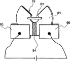
図20Aにおいて、粗動部56は、狭窄部63を支点として、粗動軸59を3個のエンコーダ28X,28Z,28Y(図示省略)によって、XYZ軸方向に移動させる構成である。粗動ストローク,移動分解能はこれらエンコーダの性能によるが、10mmのストロークで2μmの分解能は容易に得られる。上記エンコーダによる押圧力に対抗する力はバネ等により与えるが、ここでは説明を省略する。粗動部56の駆動系は、試料室壁54の横ポート54'を介して大気圧側に設けられ、ベローズ64により真空遮断されている。粗動軸59の真空室側には、延長棒30を介して微動部55が連結されている。微動部55は、Z軸方向駆動系のみで構成され、この駆動系にはバイモルフ圧電素子29が採用され、サブμmの移動分解能が得られるようにしてある。バイモルフ圧電素子29の先端部には、直径50μmφ程度の先端部を尖らせたタングステン線からなるプローブ11を連結して、バイモルフ圧電素子29に駆動電圧を与えることによって、プローブ11先端部を微動させている。
図20Bに、試料移送装置4の別の構成例を示す。本例では、粗動部56に3個のブロック状の圧電素子73(X),74(Y),75(Z)を組み合わせた構成を採用している。このブロック状圧電素子は、移動分解能はやや劣るが、移動ストロークが長く、また、反力が大きいため大きな荷重に耐えられると云う特長がある。この粗動部56に1個のバイモルフ圧電素子72'からなる微動部55を延長棒71'を介して連結し、該微動部55にプローブ11を保持させてある。
図20Bに示した試料移送装置4を試料室壁54に取り付けた例を、図20Cに示す。本例では、試料室壁54の横ポート54'を介して小型真空室54"を設けて、この中に粗動部56を設置している。試料移送装置4が不用の時には、レール110上を滑動するスライダ111を利用して試料移送装置4を試料室壁54から容易に取り外せるようにしてある。かかる構成により、試料室内には延長棒71'とその先に取り付けたバイモルフ圧電素子72'とプローブ11のみとなるため、試料室内の他のさまざまな構成部品と干渉することなくして、プローブ11を試料基板表面にアクセスさせることができる。
図21に、試料移送装置4の設置位置についての他の例を示す。同図の(a)は、試料室77の側壁54に粗動部56,微動部55からなる試料移送装置4を取付けて、試料台3上に搭載された試料基板2表面と該試料基板2表面に対向設置されたFIB照射光学系の最終電極112との間にプローブ11をアクセスさせるようにした例であり、同図の(b)は、試料室77の上壁54Aに試料移送装置4を取付けた例であり、同図の(c)は、試料移送装置4をFIB照射光学系の最終電極112の側面に取付けた例である。いずれの例にも共通している点は、試料移送装置4が試料台3上には設置されておらず、試料台3とは独立に駆動制御されるように構成されていることである。このように、試料基板2の移動に際して、試料移送装置4が試料基板2表面に接触することがないように配慮されている。
図21の(a)では、試料室77の側壁54に試料移送装置4を取付けているので試料室側壁54に横ポートが設けられていない装置であっても対応ができ、装置の構成形態に関係なく用いることができる。同図の(b)では、試料室の上壁54Aに試料移送装置4を取付けているので、試料室内空間を有効に利用でき、装置構成が異なっても対応できると云う利点がある。また、同図の(c)では、FIB照射光学系の最終電極112の側壁面に試料移送装置4を取付けているので、やはり試料室内部空間を有効に利用でき、試料室外に余計な構成部品を突出させることがなく、従って試料室外部が複雑な構成の他機種にも適用でき、装置外観を簡素にまとめることができる利点がある。
この他にも試料移送装置4の配置構成例は種々考えられるが、本構成例の基本的思想は、試料移送装置4が試料台3とは独立して設けられており、試料台3の移動に際して試料移送装置4が試料基板2表面に接触しないよう配置されているため、摘出すべき試料部分が大口径ウエハの中央部であっても、容易にアクセスが可能なことにある。
[試料ホルダの設置箇所]
試料基板2からの摘出試料片40を移送して固定すべき相手部材は、試料ホルダ19'である。この試料ホルダ19'はこれを支えるホルダカセット17'等を介して試料台3に搭載するか、もしくは、TEMステージ等の試料台3とは独立したサイドエントリ型ステージに搭載する。試料台3は、ウエハそのものを搭載できる汎用の大型試料台や、デバイスチップが搭載できる程度の小型試料台を指す。試料基板2からの摘出試料片40を試料ホルダ19'へ移送する際、試料ホルダ19'の設置位置が以後の作業性を大きく左右するので、該試料ホルダ19'の設置箇所について、以下に説明する。
ここでは、試料台3上に試料ホルダを搭載する方式(以下、試料台方式と云う)と、試料基板(ウエハ)を収容して試料室内に出し入れできるウエハカセット上に試料ホルダを搭載する方式(以下、ウエハカセット方式と云う)と、TEMステージ(またはTEM/FIB兼用ステージ)上に試料ホルダを搭載する方式(以下、TEMステージ方式と云う)とに分類して説明する。
▲1▼試料台方式
図22は試料台方式における試料ホルダの設置箇所を説明する図で、同図の(a)は上面図、同図の(b)は中央部の断面図である。本方式では、試料ホルダ19'は試料台3に着脱し易く構成されたホルダカセット17'上に搭載されている。1個のホルダカセット17'上に搭載する試料ホルダ19'の数は1個でも複数個でもよい。また、試料台3上に設置できるホルダカセット17'の数も1個でも複数個でもよい。図22では、ホルダカセット17'が1個で、試料ホルダ19'が5個の場合を示しており、各試料ホルダに摘出試料片40を3個ずつ搭載すると、1個のホルダカセット17'上に15個のTEM試料を搭載できる。
試料ホルダ19'の上面は試料基板2表面とほぼ一致させておく。それにより、摘出試料片40を移送する際に、摘出試料片40が試料ホルダ19'等と接触することはない。さらに、摘出試料片40の所望観察面は試料ホルダ19'の長手方向(試料ホルダの具体的形状については後述する)と平行とし、試料ホルダ19'の長手方向は試料台3の傾斜軸113と平行に設定しておく。この位置関係により、試料基板2からの摘出試料片40は、回転等の操作を施すこと無くして、Z方向の移動のみで試料ホルダ19'上に搭載できる。この摘出試料片40を搭載した試料ホルダ19'をTEMやSEMステージ上に載置することで、容易に所望観察面の観察ができる。
ホルダカセット17'はスライド式に試料台3上に着脱でき、操作棒及びロードロック室等を用いて、試料室内の真空を破ることなく、試料台3とは独立に、試料室外に取り出すことができる。また、この方式では、1個の試料基板2から多数のTEM試料を連続して作製することができ、ホルダカセット17'を試料室外に取り出す時には一度に多数個のTEM試料を入手できる。しかも、試料ホルダ19'上に搭載されたTEM試料は、ホルダカセット17'ごと保管庫等に一次保存することができるので、微小TEM試料の取扱いに神経を消耗させられることもない。さらに、試料基板2から摘出されたままで、まだ薄片化加工(ウォール加工)が済んでいない試料片40が多数個搭載されたホルダカセット17'を、別設のFIB装置内に搬入し、そこで仕上げ加工(ウォール加工)のみを専念して行なわせることも可能である。
図22の(b)を用いて、試料台3上における試料ホルダ19'の設置位置を説明する。摘出試料片40は、上述したウォール加工等を施すために傾斜させなければならないが、その際、試料台3が不適切な位置に設置されていると、試料移送装置4の破損等の問題を引き起こして所要の試料作製ができない。試料ホルダ19'を搭載したホルダカセット17',二次粒子検出器12,デポガス供給源8等は、常に試料移送装置4を設置した側に設置する。(図22の(b)において、試料台3の傾斜軸113より左側に設置する。)そして、試料台3の傾斜は、常に試料ホルダ19'が搭載されている側(左側)を水平状態から下げる方向にのみ動作させて、上述したような試料室内の多の構造物との干渉を避けてやる。
また、試料ホルダ19'の設置箇所に関する別方法として、TEMステージ上における試料ホルダの固定部分を含む先端部分の構造を改良し、このTEMステージを試料台3上に設置する方法も採用できる。先ず、先端部分を着脱可能に構成したTEMステージつき説明する。図23の(a)に、本実施例で用いたTEMステージ114を示す。TEMステージ114は、支柱115,握り部116,位置決め具117,試料固定具118等から構成され、試料ホルダ19'は支柱115の切り欠き部123上に搭載される。このTEMステージ114の最大の特徴は、図23の(b)に示したように、その先端部分120が分離位置119にて本体部分と着脱可能に構成されている点である。つまり、この先端部分120を本体部分から分離して試料台3上に挿着できるようにしてある。図23の(c)は、先端部分120を試料台3上に挿着した状態を示している。TEMステージ先端部分120は試料台3に設けられた挿着部121内に挿入保持される。挿着部121には、試料ホルダ19'の上方に開口部122が設けられている。試料基板2の観察所望箇所124から摘出された試料片40は、試料移送装置4のプローブ11先端部に保持されて上記挿着部121上に移送され、上記開口部122を通して試料ホルダ19'上に固定保持される。
摘出試料片40を試料ホルダ19'上へ固定後、その状態で、摘出試料片40をFIB加工により薄片化(ウォール加工)してTEM試料とする。この際、加工用FIBは、図23の(c)において紙面と垂直方向から、試料片40に照射される。
その後、この試料ホルダ19'上に固定保持された試料片40を試料室外に取り出す際には、上記挿着部121内にTEMステージの本体部分を挿入して、挿着部121内のTEMステージ先端部分120とTEMステージ本体部分とを連結させた後、このTEMステージごと試料室外に取り出し、その状態でTEM試料室内に導入してTEM観察を行う。このTEM観察時には、観察用電子ビームは、図23の(a)において、紙面と垂直方向から、試料片40に照射される。
上述した図23に示した方法によれば、TEMステージ本体部分に取り付けたり取り外したりする先端部分120のサイズは、cmオーダーであるため、手作業によっても特別に神経を使うことなく、誰にでも簡便に試料作製作業ができるという利点がある。
図24に、上記とは別形式のTEMステージを用いる場合について示す。同図の(a)に示すTEMステージ114'は、支柱115',握り部116',位置決め部117',試料固定具118'等より構成されるが、図23の(a)に示したような切り欠き部123は設けられていないので、TEM観察とFIB加工を同一ステージ上で行なうことはできない。そこで、図24の(b)に示すように、ステージ先端部分120',120"を分離位置119',119"でそれぞれTEMステージ本体部分から分離できるようにしてある。図24の(a)及び(b)では、TEM試料片40が試料固定具118'上に搭載された状態を示してあるが、まだ試料片40が搭載されていない先端部分120'を、図24の(c)に示すように、試料台3上に複数個、試料台上面(ウエハ搭載面)に垂直に、かつ試料ホルダ19'上にTEM試料40が搭載された時にそのTEM観察面が試料台傾斜軸113と平行になるようにして固定する。試料基板2の観察所望箇所124からの摘出試料片40を試料移送装置4のプローブ11先端部に保持して移送し、試料台3上に固定保持されたTEMステージ先端部分120'上の試料ホルダ19'上に固定する。その他の観察所望箇所からの摘出試料片についても同様である。図24の(c)に示した例では、試料台3上には7個の試料ホルダ19'が搭載されており、各試料ホルダ19'上にそれぞれ3個の摘出試料片40を固定すれば、合計21個のTEM試料を同一試料室内で連続して作製することができる。
▲2▼ウエハカセット方式
図25にウエハカセット方式の装置構成例を示す。本方式では、ウエハカセット125に試料ホルダ19'を保持したホルダカセット17'を装着するようにしている。ここで、ウエハカセット125は、1枚のウエハ(試料基板)2を収容するための専用トレイであるため、このウエハカセット125内に収容されたウエハは直接装置部品や人手に触れることはない。また、このウエハカセット125は各種プロセス装置にそのまま出し入れすることができ、ウエハの装置間移動に際しても用いられる。図25に示すように、ホルダカセット17'をウエハカセット125のホルダカセット装着部121'に着脱可能に構成しておくことによって、ウエハ交換時に加工済みのTEM試料を搭載した複数の試料ホルダ19'を入手することができる。ここで、ウエハカセット125とホルダカセット17'との対応関係,ホルダカセット17'とそれに搭載されている試料ホルダ19'との対応関係及び試料ホルダ19'とそれに固定されている摘出試料片40との対応関係を常に管理しておくことで、例えばTEM観察等の観察,計測,分析を行なった結果得られた情報とウエハ2の試料摘出位置との対応関係を容易に把握することができる。
▲3▼TEMステージ方式
本方式では、試料台3とは独立に動作するステージ上に試料ホルダ19'を装着する。この独立動作するステージとは、例えばサイドエントリ型のTEMステージ等を指す。本例では、このサイドエントリ型TEMステージを試料室内に出し入れ可能なように構成してある。この場合、サイドエントリ型TEMステージの回転軸を試料台3の傾斜軸と平行になるよう設定する。なお、摘出試料片の観察所望領域が上記サイドエントリ型TEMステージの回転軸上に配置されるのが望ましいが、試料ホルダ上に搭載される摘出試料片は数μm〜30μm程度と微小であるため、実質的には試料ホルダの試料固定面がサイドエントリ型TEMステージの回転軸上に来るように配置しておけばよい。かかる構成により、試料基板からの摘出試料片は、回転等の操作を要することなくして、Z方向の移動のみで試料ホルダ上に搭載できるため、試料移送装置に傾斜機構や回転機構等の煩雑な機構を付加する必要がなくなり、試料移送装置の構成を簡素化できると云う利点がある。また、本方式の場合、摘出試料片を試料ホルダ上に固定したら、TEMステージを試料室から引き抜いて、そのままTEM装置内に装着できるので、TEM観察に至るまでに熟練や時間を要する手作業が必要でないので、試料作製に要する時間を大幅に短縮でき、また、試料作製時の精神的負担を軽減できると云う効果が得られる。また、試料片の観察部(ウォール部)が厚過ぎる等でTEM観察しにくい場合には、TEMステージをそのまま本試料作製装置の試料室内に再挿入するだけで、直ちにFIB照射による再加工を施すことができると云う簡便さを有する。
[試料ホルダの形態]
従来のTEM用試料ホルダとしては、図7の(a)に示した単孔型や同図の(b)に示したメッシュ型等が知られている。単孔型ホルダ78は、薄肉金属円板の中央部に直径1mmφ程度の孔79を設けたものである。この単孔型ホルダを用いる場合には、試料片を孔79の内壁面上に正確に位置決めして取り付ける必要があるが、本発明の試料作製方法により得られる試料片のようにそのサイズが10〜20μmと小さいと、この取付作業が非常に難しい。メッシュ型ホルダ109は、薄肉金属円板の中央開口部に金属メッシュ109'を張ったものであり、試料片のサイズに合わせた網目間隔のメッシュを用いれば、試料片の取付位置はある程度任意に選ぶことができるが、試料透過電子線の経路がメッシュ構成部材に遮断されてしまって観察所望領域のTEM観察ができなくなるおそれがある。
本発明による試料作製方法では、摘出試料片のサイズ(高さ)が10〜20μmと小さいため、ホルダの試料固定面に深さ20μm以上の凹部があると、摘出試料片はこの凹部に埋もれてしまい、TEM観察の際に観察用電子線が遮断され、折角試料基板から摘出した試料片のTEM観察ができなくなってしまう。そこで、本実施例では、図26に示すような試料ホルダを用いた。つまり、ここではFIB加工に際してのFIB照射方向とTEM観察に際しての観察用電子線の入射方向とが互いに直角方向となるようにして、両ビームが遮断されないようなホルダ構造とし、かつ、特に観察用電子線を照射し易いようにするために試料固定面の平坦性を良くしている。
図26の(a)に示したホルダ126は、シリコンウエハからへき開やダイシングソーを用いて切り出した短冊状シリコン片127上に摘出試料片40を保持させるものである。本例でのホルダ126の大きさは、長さ2.5mm,幅50μm,高さ0.5mm(シリコンウエハ厚)である。このように、シリコンウエハの研磨面を摘出試料片40の固定面とすることによって、この固定面の凹凸を小さくできるので、TEM観察に際して、観察用電子線の照射が阻害されることがない。なお、ホルダ形状及び寸法は、上例に限定されるものではなく、要は、シリコンウエハの研磨面を試料片40の固定面とすること、およびホルダ幅をできだけ薄くすることである。
図26の(b)に示すホルダ128は、図26の(a)のホルダ126の一変形例である。ホルダ126では、TEM観察時にホルダの僅かな傾きにより観察用電子線の照射が阻害されるのを避けるために、ホルダ幅をできるだけ薄くすることが望ましいが、該ホルダ幅を極端に薄くすると機械的強度が小さくなり、ホルダの取扱時に破損する等の問題が発生する。そこで、図26の(b)のホルダ128では、十分な機械的強度を持ちかつ電子線照射の邪魔にならないホルダ構造として、シリコンウエハから切り出した短冊状シリコン片129を幅広の下方部分129Aと幅狭の上方部分129Bとからなる凸型断面形状に加工したものを用い、その幅狭上方部分129Bの上面(元のウエハの研磨面)に摘出試料片40を搭載するようにしている。なお、図26の(b)は、ホルダ128上に摘出試料片40を複数個(3個)搭載した状態を示している。
図26の(c)に示すホルダ130は、半円形状のシリコン板131で形成されており、これはシリコンウエハからへき開およびウエットエッチング技術を利用して作製した。その直径は約3mm,厚さは約50μmである。摘出試料片40の固定面は、元のウエハのへき開面であり十分な平滑性を有している。このホルダ130は半円形状であるため、リング状のワッシャを用いることによってTEMステージ上に容易に搭載することができる。
図26の(d)に示すホルダ132は、半円形状の金属基板133の側面に図26の(a)に示したホルダ126を取り付けた構造である。半円形状金属基板133は厚さ50μm,直径3mmの薄片であり、これに取り付けたホルダ126は長さ2mm,幅50μm,高さ0.5mm程度の短冊状シリコン片127から成る。ホルダ126の基板133への取付けには導電性接着材を用いたが、それに限定されるものではない。なお、ホルダ126は、短冊状シリコン片127の上面が金属基板133の上端面よりも上方に出るようにして取り付け、TEM観察用電子線が金属基板によって遮断されるのを避けた。本例のホルダ126においても、摘出試料片40の固定面は、元のシリコンウエハの研磨面であり、十分に平滑である。また、金属基板133の上端面には直接摘出試料片40を固定しないがため、この面には多少凹凸があってもTEM観察には全く支障がない。このため、金属基板133の作製には殆ど神経を使う必要はなくなり、打抜き法やウエットエッチング法,放電加工法等により容易かつ安価に作製することができる。なお、図26の(d)には、金属基板133に図26の(a)のホルダ126を取り付けた例を示したが、図26の(b)のホルダ128を取り付けた場合にも全く同様の効果が得られる。
以上、TEM観察用の試料ホルダの形状について4例を示したが、それらの基本思想とするところは、試料固定面を極力平滑とし、かつ試料固定面の幅をなるべく薄くしたことであり、この基本思想に沿っての種々の改変がなされ得ることは云うまでもない。
<実施例5>
試料基板から微小試料片を摘出するためには、摘出する試料片の底面を基板から分離する工程(以下、底浚い工程と呼ぶ)が必須である。先に図4で説明した従来のFIBによる底浚い加工法(公知文献3参照)では、基板2表面に対し斜め方向からFIBを照射して底浚い加工をするため、摘出された試料片40の底面には、底浚い加工時のビーム入射角と加工アスペクト比によって決まる傾斜がつく。上記従来法では、底浚いする(分離用の溝34を形成する)ために、試料基板を大きく(約70゜)傾斜させている。FIBの集束性から要求される対物レンズと試料基板との間隔を考慮すると、このような大傾斜はFIB性能を劣化させてしまい、満足な加工ができないと推察される。通常用いられているFIB装置性能を維持するには、試料基板傾斜角は60゜程度が限度である。また、直径300mmにも及ぶ大口径ウエハ用の試料ステージを70゜も大きく傾斜させることは、機構的にも非常に困難である。また、たとえ70゜の大傾斜が可能であったとしても、摘出試料片の底面は20゜の傾斜を持つため、この摘出試料片を試料ホルダの水平保持面上に搭載すると、試料片表面は試料ホルダの水平保持面に対し20゜も傾斜してしまうことになり、該試料片にその表面に対しほぼ垂直な溝やウォールを形成することが困難となる。試料基板表面に対してほぼ垂直な溝やウォールを形成するためには、この試料片底面の傾斜を小さくし、試料片底面を試料片表面に平行に近くすることが必須である。しかし、そのためには、上述の底浚い加工時の試料基板の傾斜角をさらに大きくしなければならず、これは上述した装置構成上の制約からさらに困難になる。従って、本発明で目指すような摘出試料片を別の部材(試料ホルダ)上に搭載して観察装置や分析装置内に導入するためには、水平底面(または垂直側面)が形成できるような別の底浚い方法を検討しなければならない。(但し、公知文献3では、摘出試料片を試料ホルダ等に搭載することなく、試料移送装置のプローブ先端部に固定保持したままで観察しているため、試料底面の形状には何ら影響されない。)
このような状況から、本実施例では、試料台を極端に大きく傾斜させることなくして、底浚い加工法により微小試料を摘出できる方法を検討した。
以下に本実施例による試料作製方法の具体的手順について説明する。ここでは、TEM観察用試料の作製方法を例にとり、TEM観察すべき領域のマーキングから最終的なウォール加工までの全てをFIBを用いて行なう方法について説明する。また、手順を明確にするために、以下幾つかの工程に分けて、図27を用いて説明する。
(1)マーキング工程:
本試料作製方法では、試料基板からTEM観察すべき領域を含んだ微小試料片を分離摘出することを前提としている。このため、試料基板から分離摘出後の試料片にTEM観察すべき領域の薄片化加工(ウォール形成)を施す際に、上記のTEM観察すべき領域の位置が特定できなくなってしまうおそれがある。このため、観察領域の位置を特定するためのマーキングが必要となる。試料基板がウエハやチップそのままの状態では、CADデータ等からの位置割り出しや、光学顕微鏡像,走査イオン顕微鏡像(SIM像)等による位置確認が可能であるため、最初に試料基板上の観察領域(ウォール形成領域)にマーキングを施しておく。このマーキングは例えばウォール形成領域の両端にFIB加工やレーザ加工等でマークを施すことにより行なう。本実施例では、観察領域を挟んで10μm間隔で2個の十字状マーク134,134'を施した。上記2個のマーク間を結ぶ直線が試料台傾斜軸と平行になるように事前に試料台を回転調整しておく。また、このマーキング工程の際、ウオール146の保護の目的で、予めマーク134,134'間にデポジション膜(図示せず)を形成しておいてもよい。(図27の(a))
(2)矩形穴加工工程:
上記2個のマーク134,134'を結ぶ直線の延長上で、上記2個のマークの両外側にFIB135の照射により2個の矩形穴136,136'を設ける。この矩形穴の開口寸法は、例えば面積10μm×7μm,深さ15μm程度で、両矩形穴間の間隔は30μmとした。なお、短時間に穴加工ができるようにするために、ビーム径0.15μm程度,ビーム電流約10nAの大電流FIBで穴加工した。所要加工時間はおよそ7分であった。(図27の(a))
(3)垂直溝加工工程:
次に、上記マーク134,134'間を結ぶ直線より約2μmを隔てそれと平行に、かつ一端が矩形穴136'に達し他端が矩形穴136には僅かに達しないようにして、FIB走査によって幅約2μm,長さ約28μm,深さ約15μmの細長い垂直溝137を形成する。FIBの走査方向は、FIB照射により発生するスパッタ粒子が折角形成した垂直溝137や、矩形穴136,136'を埋めることがないようにする。一方の矩形穴136と垂直溝137との間に残された幅が2μm程度の残存領域138は、後に、上記観察領域を含む試料片40を試料基板2から分離する際、試料片40を仮保持しておくための支持部となる。(図27の(b))
(4)傾斜溝加工工程:
上記(2),(3)の工程で水平に保たれていた試料基板面を小さく傾斜(本例では20゜)させてから、上記マーク134,134'間を結ぶ直線から約2μmを隔てそれと平行に、かつ、先に形成した垂直溝137とは反対の側に、FIB照射によって傾斜溝139を形成する。ここで、上記した2個のマーク134,134'間を結ぶ直線は試料台(図示省略)の傾斜軸と平行に設定されているので、垂直溝137側に対し傾斜溝139側が上となるように試料基板面を傾斜させる。傾斜溝139は、両矩形穴136,136'間を結んで、幅約2μm,長さ約30μm,深さ約18μmで形成した。この際も、FIB照射により発生するスパッタ粒子が折角形成した矩形穴136,136'や垂直溝137や傾斜溝139を埋めることがないように留意する。傾斜溝139はその底部で先に形成した垂直溝137底部と交わり、その結果、マーク134,134'を含んだ、底部頂角が20゜の直角三角形断面のクサビ型試料片140が、支持部138だけを残し、試料基板2から分離され、支持部138によって片持ち支持された状態となる。(図27の(c))
(5)プローブ固定用デポ工程:
次に、試料基板面を水平に戻してから、試料片140の支持部138とは反対側端部に試料移送装置のプローブ141の先端部を接触させる。この接触状態は試料片140とプローブ141との間の導通や両者間の容量変化によって感知することができる。また、不注意なプローブ141の試料面への押付けにより試料片140やプローブ141が破損されるのを避けるために、プローブ141が試料片140に接触した時点で直ちにプローブ141の垂直方向駆動(押し下げ)を停止させる機能を設けておく。次いで、試料片140にプローブ141先端部を固定接続するために、プローブ141先端部を含む約2μm角の領域に、デポジション用ガスを供給しながら、FIB135を照射(走査)して、該FIB照射領域にデポ膜142を形成する。このデポ膜142を介してプローブ141先端部と試料片140とが固定接続される。(図27の(d),(e))
(6)試料片摘出工程:
試料片140を試料基板2から摘出するために、試料片140を仮保持している支持部138にFIB135を照射して、スパッタ加工により支持部138を除去して、試料片140を仮保持状態から開放させる。支持部134は、試料基板面上で2μm平方,深さ約15μmであるので、約2〜3分のFIB照射(走査)で除去できる。これにより、試料片140は、試料基板2から完全に分離摘出された状態となる。(図27の(e),(f))
(7)摘出試料片移送(試料ステージ移動)工程:
次いで、試料基板2から分離摘出された試料片140をプローブ141先端部に固定接続した状態で試料ホルダ143上に移動させるが、これは、実際には試料台側を移動させて、該試料台上に載置された試料ホルダ143をFIB135の走査範囲内に移動させる。この時、不慮の事故を避けるため、試料片140をプローブ141とともに、矢印で示すように上方に退避させておく。ここで、試料台上への試料ホルダ143の設置方式には前述したように種々の方式があるが、本例では、サイドエントリ型のTEMステージ上に試料ホルダ143が設置されている場合を想定している。(図27の(f),(g))
(8)摘出試料片固定工程:
試料台移動により、試料ホルダ143がFIB135の走査範囲内に入ったら、その位置で試料台の移動を停止してから、プローブ141を下方に押し下げ、試料片140を試料ホルダ143上面へと接近させる。(図27の(g))
試料片140が試料ホルダ143上面に接触したら、両者の接触部位にデポガスを導入しながらFIB135を照射してデポ膜145を形成し、このデポ膜145を介して試料片140を試料ホルダ143上に固定接続する。本実施例では、試料片140の長手方向端面部にデポ膜145を形成した。この時のFIB照射領域は3μm平方程度である。形成されたデポ膜145は、その一部で試料ホルダ143上に、他の一部で試料片140の側面に付着して、両者間を固定接続する。なお、試料片140をより確実に試料ホルダ143に固定するために、試料ホルダ143の試料固定面に幅2μm×長さ32μm×深さ3μm程度の細長溝144をFIB加工により事前に形成しておき、該細長溝144内に試料片140の下端部を挿入した上で、試料片140の長手方向端面部にデポ膜145を形成するようにしてもよい。図には、この後者の場合を示してある。(図27の(g),(h))
また、試料片140中の観察領域がサイドエントリ型TEMステージの回転中心軸上に配置されることが望ましいが、試料ホルダ143上に固定接続すべき試料片140が数μmから数10μm程度と微小であるがため、実質的には、試料ホルダ143の試料固定面がサイドエントリ型TEMステージの回転中心軸上に来るように配置しておけばよい。このようにすることにより、TEMステージをTEM内に設置した時に、試料片140中の観察所望領域を容易にTEMの観察視野内に導入することができる。
また、この時、サイドエントリ型TEMステージの回転中心軸を試料台の傾斜軸に平行にしておくと摘出試料片の方向を回転させる必要がなくなるので、試料移送装置に複雑な回転機構を設ける必要がない。さらに、サイドエントリ型TEMステージを用いることによって、試料作成後直ちにTEM内に導入でき、また、追加工が必要な場合には、直ちに再度FIB装置内に戻して追加工ができるという効果がある。
(9)プローブ切り離し工程:
次に、上記したデポガスの供給を停止した後、プローブ141と試料片140とを固定接続しているデポ膜145にFIBを照射して、該デポ膜145をスパッタ除去することで、プローブ141を摘出試料片140から切り離す。これにより、試料片140は試料ホルダ143上に固定保持されて、プローブ141からは完全に自立する。(図27の(i))
(10)ウオール加工工程:
最後に、FIB照射によって、試料片の観察所望領域が厚さ100nm以下程度のウォール146になるように薄く仕上げ加工して、一連のTEM試料作製工程を完了する。この時、試料片140の長手方向側面の一方が垂直面であるため、ウォール加工のためにFIB照射領域を決定する際、この垂直面を基準にすることで、元の試料基板表面にほぼ垂直なウォール146を形成できる。また、FIB照射に先立って、ウォール面をより平面的に加工するためにウォール形成領域を含む試料片上面にFIBデポ膜を形成しておくとよい。上述したウォール加工の結果、横幅約15μmで,深さが約10μmのウォール146を形成でき、TEM観察用試料とすることができた。(図27の(j))
以上のマーキング工程からウォール加工工程までの全工程に要する時間は、約1時間30分であり、従来のTEM試料作製方法に比べて所要時間を数分の1に短縮できた。
(11)TEM観察工程:
上記したウォール加工終了後、試料作製用FIB装置の試料室内からサイドエントリ型TEMステージを引き抜き、TEMの試料室内に導入する。この時、観察用電子線経路と、ウォール面とが垂直に交わるようTEMステージを回転させて挿入する。その後のTEM観察技術についてはよく知られているので、ここでは説明を省略する。
なお、上記した本実施例における試料作製手順は、TEM観察用試料に限らず、その他種々の観察手法や、分析,計測手法における試料作製に用いることも可能である。
なお、本実施例による試料作製方法が公知文献3における試料作製方法と大きく異なる点は、(1)試料の摘出(分離)に際してのビーム照射方法が全く異なり、本実施例では、摘出試料片をなるべく薄くするためと、試料基板からの試料片底面の分離(底浚い)を簡便にするために、試料片長手方向(TEM観察面に平行方向)の側面を傾斜加工している点,および、(2)本実施例では、摘出試料片は試料移送装置のプローブとは全く別部材である試料ホルダ上に固定保持される点である。
このように、本実施例による試料作製方法によれば、試料基板(半導体ウエハやデバイスチップ等)の所望の観察または分析領域をマーキングしたその場にて直ちにその試料基板から、人の手作業を介することなく、かつ試料基板を試料作製装置の真空試料室から外部に出すことなく、TEM観察用やその他の分析/計測/観察のための試料を作製することできる。また、本実施例による試料作製装置を用いることで、マークキング工程からウォール加工までの全ての試料作製工程を同一試料作製装置内で一貫して行なえるため、研磨作業や試料片の試料ホルダへの取付け等の熟練技能と長時間を要する手作業を介することなく、また、試料の装置間移動に伴なう試料落下等の危険性を軽減して、半導体ウエハや半導体チップを始め、その他の材料や部品からの試料片の摘出から試料ホルダ上への搭載までを行なうことができる。特に、TEM試料の作製に関して、試料作製所要時間を大幅に短縮できる効果が得られる。
<実施例6>
試料基板から試料片を摘出するために試料移送装置によってプローブを試料基板表面へ接触させる際には、試料基板を破壊,損傷させないように細心の注意を払う必要がある。本実施例は、試料基板を破損させないように配慮された試料移送方法および移送装置に関するものである。
図28に本実施例における試料移送装置(マニピュレータ)の概略構成を示す。図において、試料移送装置4は、摘出試料片を保持するプローブ11と、プローブ11を3軸(X,Y,Z)方向に粗移動させる粗駆動部147と、プローブ11を1軸(Z)方向に微移動させる微駆動部148とから成っている。粗駆動部147は試料台(図示省略)から十分離れた位置に設置されており、微駆動部148に取り付けられたプローブ11が試料台上の広い範囲にわたりアクセスできるようにするために、微駆動部148は長い延長棒149を介して粗駆動部147に連結されている。
粗駆動部147は、X軸方向粗動部147X,Y軸方向粗動部147Y,Z軸方向粗動部147Zから構成されており、各軸方向の移動ストロークは約3mmで、移動分解能は約0.5μmである。微駆動部148は、バイモルフ圧電素子により構成されており、移動ストロークは約200μm、移動分解能は約0.05μmである。
上述したように、微駆動部148を延長棒149を介して粗駆動部147に連結する構成としたのは、以下のような理由による。すなわち、本発明の試料作製装置において用いられるイオンビーム照射光学系の最終段レンズ電極と試料台との間やその周辺には種々の装置部品が混在設置されている。このような種々の装置部品との設置場所についての競合を避けるため、本実施例における試料移送装置4の本体部分である粗駆動部147は、できるだけ試料台から離れた位置に設置されるのが望ましいからである。本実施例では、延長棒149を用いることにより、粗駆動部147を試料台から十分に離して設置できるようにしている。
以下、図29を用いて、プローブ11先端部を試料基板2表面へ接触させる手順について説明する。図29において、破線150が基板2表面と交差する点151がプローブ11の接触目標位置である。
図30に、図29に示した手順(a)〜(f)に対応させたフローを示す。なお、図30において、矢印に付された記号「Y」は、その事象が起こったこと(例えば、「接触確認」の場合は、接触確認がなされたこと)を示し、記号「N」はその事象が起こっていないこと(例えば、「接触確認」の場合には、接触確認されていないこと)を示している。また、図30における「接触」とは、特に断わりがない場合、にはプローブ11と試料基板2との間での接触を指す。なお、実際には、プローブ11−試料基板2間の接触状態は常にモニタされており、接触確認作業は常時行なわれている。従って、接触が起こり次第、記号「Y」で示される動作が行われる。以下の説明では、この「接触確認」が多数回出てくるため、説明が冗長となるのを避けるため、特別の場合を除き、この点についての詳しい説明は省略する。
先ず始めに、プローブ11先端部が基板2表面に接触していないことを確認した上で、X軸方向粗動部147X,Y軸方向粗動部147Yを駆動してプローブ11先端部を接触目標位置151の真上まで移動する(a)。次に、プローブ11先端部が基板2表面から微駆動部148の全ストローク以上離れている状態において、微駆動部148を駆動してプローブ11先端部をその原点位置からZ0(例えば、微駆動部148の全ストロークの50%程度、本実施例の場合は100μm程度)だけ基板2表面に近づけた状態にする(b)。その後、Z軸方向粗動部147Zを駆動して、プローブ11先端部が基板2表面に接触するまで微駆動部148を基板2表面に接近させる(c)。両者間での接触は、例えば、プローブ11と基板2との間の電気抵抗変化をモニタすることによって、あるいは、プローブ11に電圧を印加しておいて基板2表面の2次電子像上での電位コントラスト変化をモニタすることによって検知することが可能である。このようにして、プローブ11先端部と基板2表面との接触が検知されたら、即座にZ軸方向粗動部147Zの駆動を停止させると共に、微駆動部148を再駆動して、プローブ11先端部をその原点位置(0μm位置)まで退避(上方後退)させる。この微駆動部の退避によって、Z軸方向粗動部147Zの停止遅れやドリフト等によりプローブ11−基板2間の多少の余剰接近があっても、上記した微駆動部退避分(約100μm)でプローブ11先端部が基板2表面から十分離れた状態になるため、両者が損傷を受けずに済む。即ち、この場合には、Z軸方向粗動部147Zの停止遅れ等による余剰接近分よりも充分大きなストロークを有する微駆動部148を使用する必要がある。例えば、本実施例による試料移送装置(プローブ駆動機構)4の場合には、Z軸方向粗動部147Zの余剰接近分は1μm以内であり、微駆動部148のストロークは200μmあり、その50%に当たる100μmを微駆動部退避量としているから、上記の余剰接近による損傷を回避するには充分である。ここで、さらに安全を図るために、Z軸方向粗動部147Zの動作をロックし、このロックの解除を能動的に行なわない限りZ軸方向粗動部147Zは再駆動できないようにしておく(d)。この状態で、X軸方向粗動部147X及びY軸方向粗動部147Yを駆動してプローブ11先端部の接触目標位置151の真上への最終的な位置合わせを行なう(e)。その後は、微駆動部148のみを駆動して、プローブ11先端部を基板2表面に軟接触させる(f)。この様に、最終接触を微駆動部148のみを用いて行なうことができるため、基板表面及びプローブ11先端部の破損を抑制することができる。
図30の(g)は、接触後に位置ずれが生じていた場合の調整法のフローであり、図29では、この調整手順の図示は省略されている。図30の(g)において、接触位置がずれていた場合には、微駆動部148を上方に退避させ、プローブ11先端部の基板2表面との接触を解く。ここで、もし微駆動部148が原点位置(0μm位置)に戻ってもまだ接触したままの場合には、Z軸方向粗動部147Zのロックを解除してZ軸方向粗動によるプローブ11先端部の退避を行ない、改めて、上述したZ軸方向粗動による接近操作からやり直す。微駆動部148による微動退避のみで接触が解けた場合には、その後、念のために、微駆動部148によりプローブ11先端部をさらにZ1程度上方に後退させる。Z1の値は、プローブ11先端部のX,Y面内移動量と基板2表面の凹凸高さから決定されるが、本実施例の場合は3μm程度とした。しかる後に、X軸方向粗動部147X,Y軸方向粗動部147Yを駆動して接触目標位置151の真上にプローブ11先端部を移動させてから、微駆動部148によってプローブ11先端部を基板2表面に接近させ、両者を接触させる。
ここで、上記の粗動停止遅れやクリープ現象による余剰接近量が事前に見積もれる場合には、図29の(d)における微動退避は、必ずしもZ0位置(100μm位置)から原点位置(0μm位置)までの100μmもの大きな退避量とする必要はない。例えば、上例において、上記原因による余剰接近量が5μm以下と見積もれるならば、10μm程度の退避量(100μm位置から90μm位置までの退避)でも十分である。また、これ以外にも、一旦、微駆動部148を原点位置(0μm位置)まで戻してから、改めて90μm位置近くまで比較的高速でプローブ11を基板2表面に接近させ、それ以降は十分に低速で100μm位置近くまで接近させることによって、プローブ11先端部を基板2表面接触させるという速度変化法を用いてもよい。この場合には、接触時におけるプローブの接近速度が小さいため、より基板破損の確率が減り、また微駆動部の総合駆動時間を短縮することが可能になる。
また、もし微駆動部148によるプローブ11の微駆動が、X,Y面内での微動移動も伴なう場合には、手順(d)におけるプローブ11の微動退避後の、手順(e)におけるX,Y軸方向粗動によるプローブ11先端部の接触目標位置151の真上への移動には意味がなくなる。従って、その場合には、手順(b)でのZ0位置への微動接近の後に、X軸,Y軸方向粗動によってプローブ11先端部と接触目標位置151上方への移動を行い、その後に手順(c),(d)を実行し、その次の手順(e)は省略して、手順(f),(g)へと進めるようにした方がより効率的である。
以上では、プローブ11先端部の基板2表面への接触について述べたが、試料片摘出後に、摘出試料片40を試料ホルダ19に接触させる際にも、プローブ11をプローブに固定された試料片40に、基板2表面を試料ホルダ19表面にそれぞれ置き換えるだけで、上記と全く同様の接触法を用いることができ、その場合にも、上記と同様に、試料片および試料片ホルダの損傷を効果的に抑制できることは云うまでもない。
以上のような接触法を用いることで、プローブ,基板および試料片ホルダの破損を抑制しての効率的な試料片摘出が可能になる。
以上本発明の種々の実施例について説明してきたが、本発明は上記実施例に限定されるものではなく、例えば、上記実施例では、主としてTEM観察用試料の作製について説明したが、その他の観察装置(例えば、SEM等)や分析/計測装置用の試料の作製にも本発明を適用できることは明らかである。
以上説明してきたように、本発明によれば、集積回路チップや半導体ウエハ等の試料基板から、人の手作業を介することなくして、直接に、TEM等の観察位置やその他各種の分析/計測装置用の試料を作製することができる。また、摘出試料片をカートリッジ上に保持できるため、試料片の保守管理を容易にでき、さらに試料片の観察,分析時に外部からの機械振動等の影響を軽減することができる。
付記:
1.試料基板の観察すべき領域の近傍部にプローブ先端部を固定接続するプローブ接続工程と、上記観察すべき領域を含む試料片を上記プローブ先端部に固定接続された状態で上記試料基板から分離する試料片分離工程と、この分離された試料片を観察装置の試料ホルダに固定する試料片固定工程と、上記試料ホルダに固定接続された上記試料片から上記プローブ先端部を分離するプローブ分離工程とを含んでなることを特徴とする試料作製方法。
2.上記プローブ分離工程の後に、上記試料片の上記観察すべき領域を含む部分の追加工を行なう追加工工程をさらに含んでなることを特徴とする上記1に記載の試料作製方法。
3.上記プローブ分離工程の前に、上記観察すべき領域を明示するためのマーキングを行なうマーキング工程をさらに含んでなることを特徴とする上記1または2に記載の試料作製方法。
4.上記試料片分離工程における上記試料基板からの上記試料片の分離は、イオンビームスパッタ加工法によって行なわれることを特徴とする上記1から3までのいずれかに記載の試料作製方法。
5.上記イオンビームスパッタ加工法による上記試料基板からの上記試料片の分離は、集束イオンビーム(FIB)を用いて行なわれることを特徴とする上記4に記載の試料作製方法。
6.上記イオンビームスパッタ加工法による上記試料基板からの上記試料片の分離は、成形イオンビーム(PJIB)を用いて行なわれることを特徴とする上記4に記載の試料作製方法。
7.上記イオンビームスパッタ加工法による上記試料基板からの上記試料片の分離は、集束イオンビーム(FIB)および成形イオンビーム(PJIB)を併用して行なわれることを特徴とする上記4に記載の試料作製方法。
8.上記イオンビームスパッタ加工法による上記試料基板からの上記試料片の分離は、上記試料基板の表面に対して互いに異なる複数の角度からイオンビームを照射することによって行なわれることを特徴とする上記4から7までのいずれかに記載の試料作製方法。
9.上記試料片分離工程における上記試料基板からの上記試料片の分離は、イオンビーム加工法とレーザビーム加工法とを併用して行なわれることを特徴とする上記1から3までのいずれかに記載の試料作製方法。
10.上記試料片分離工程における上記試料基板からの上記試料片の分離は、上記試料基板の上記試料片として分離すべき部分の周囲に当該部分を囲む溝を形成し、この溝により囲まれた部分に機械的剪断力を加えて上記部分を剪断分離することによって行なわれることを特徴とする上記1から3までのいずれかに記載の試料作製方法。
11.上記プローブ接続工程における上記試料基板の上記観察すべき領域の近傍部への上記プローブ先端部の固定接続は、上記プローブ先端部を上記試料基板の上記観察すべき領域の近傍部表面に接触させ、この接触部にイオンビームアシストデポジション膜を形成させることにより行なわれることを特徴とする上記1から3までのいずれかに記載の試料作製方法。
12.上記プローブ分離工程における上記試料片からの上記プローブ先端部の分離は、上記試料片の表面に上記プローブ先端部を固定接続している上記イオンビームアシストデポジション膜をイオンビームスパッタ加工法を利用して除去することによって行なわれることを特徴とする上記11に記載の試料作製方法。
13.上記プローブ接続工程における上記試料基板の上記観察すべき領域の近傍部への上記プローブ先端部の固定接続は、上記プローブ先端部を上記試料基板の上記観察すべき領域の近傍部表面に接触させ、この接触部にイオンビームスパッタ粒子再付着膜を形成させることによって行なわれることを特徴とする上記1から3までのいずれかに記載の試料作製方法。
14.上記プローブ分離工程における上記試料片からの上記プローブ先端部の分離は、上記試料片の表面に上記プローブ先端部を固定接続している上記イオンビームスパッタ粒子再付着膜をイオンビームスパッタ加工法を用いて除去することにより行なわれることを特徴とする上記13に記載の試料作製方法。
15.上記プローブ接続工程における上記試料基板の上記観察すべき領域の近傍部への上記プローブ先端部の固定接続は、上記プローブ先端部を上記試料基板の上記観察すべき領域の近傍部表面に静電吸着法を利用して吸着させることによって行なわれることを特徴とする上記1から3までのいずれかに記載の試料作製方法。
16.上記プローブ分離工程における上記試料片からの上記プローブ先端部の分離は、上記試料片の表面に上記プローブ先端部を固定接続している上記静電吸着法による吸着力を減殺することにより行なわれることを特徴とする上記15に記載の試料作製方法。
17.上記プローブ接続工程における上記試料基板の上記観察すべき領域の近傍部への上記プローブ先端部の固定接続は、上記プローブ先端部を付着させた粘着材を介して行なわれることを特徴とする上記1から3までのいずれかに記載の試料作製方法。
18.上記プローブ分離工程における上記試料片からの上記プローブ先端部の分離は、上記試料片の表面に上記プローブ先端部を固定接続している上記粘着材による粘着力を減殺することによって行なわれることを特徴とする上記17に記載の試料作製方法。
19.上記粘着材が紫外線照射によってその粘着力を減じる紫外線剥離型粘着材であり、上記プローブ分離工程における上記試料片からの上記プローブ先端部の分離は、上記試料片の表面に上記プローブ先端部を固定接続している上記紫外線剥離型粘着材に紫外線を照射することによって行なわれることを特徴とする上記17に記載の試料作製方法。
20.上記粘着材が加熱によってその粘着力を減じる加熱剥離型粘着材であって、上記プローブ分離工程における上記試料片からの上記プローブ先端部の分離は、上記試料片の表面に上記プローブ先端部を固定接続している上記加熱剥離型粘着材を加熱することにより行なわれることを特徴とする上記17に記載の試料作製方法。
21.上記プローブ接続工程における上記試料基板の上記観察すべき領域の近傍部への上記プローブ先端部の固定接続は、上記プローブ先端部を上記試料基板の上記観察すべき領域の近傍部表面に融着させることにより行なわれることを特徴とする上記1から3までのいずれかに記載の試料作製方法。
22.上記プローブ分離工程における上記試料片からの上記プローブ先端部の分離は、上記プローブ先端部と上記試料片表面との融着部をイオンビームスパッタ加工法を用いて除去することにより行なわれることを特徴とする上記21に記載の試料作製方法。
23.上記プローブ接続工程における上記試料基板の上記観察すべき領域の近傍部への上記プローブ先端部の固定接続は、上記プローブ先端部を上記試料基板の上記観察すべき領域の近傍部表面に金属接合させることにより行なわれることを特徴とする上記1から3までのいずれかに記載の試料作製方法。
24.上記プローブ分離工程における上記試料片からの上記プローブ先端部の分離は、上記プローブ先端部と上記試料片表面との金属接合部をイオンビームスパッタ加工法を用いて除去することにより行なわれることを特徴とする上記23に記載の試料作製方法。
25.上記試料片固定工程における上記試料片の上記試料ホルダへの固定は、上記試料片を上記試料ホルダに接触させ、その接触部にイオンビームアシストデポジション膜を形成させることにより行なわれることを特徴とする上記1から3までのいずれかに記載の試料作製方法。
26.上記試料片固定工程における上記試料片の上記試料ホルダへの固定は、上記試料片を上記試料ホルダに接触させ、その接触部にイオンビームスパッタ粒子再付着膜を形成させることにより行なわれることを特徴とする上記1から3までのいずれかに記載の試料作製方法。
27.上記試料片固定工程における上記試料片の上記試料ホルダへの固定は、上記試料片を上記試料ホルダに静電吸着法を利用して吸着させることにより行なわれることを特徴とする上記1から3までのいずれかに記載の試料作製方法。
28.上記試料片固定工程における上記試料片の上記試料ホルダへの固定は、上記試料片を上記試料ホルダに粘着材を介して粘着させることにより行なわれることを特徴とする上記1から3までのいずれかに記載の試料作製方法。
29.上記試料片固定工程における上記試料片の上記試料ホルダへの固定は、上記試料片を上記試料ホルダに融着させることにより行なわれることを特徴とする上記1から3までのいずれかに記載の試料作製方法。
30.上記試料片固定工程における上記試料片の上記試料ホルダへの固定は、上記試料片を上記試料ホルダに金属接合させることにより行なわれることを特徴とする上記1から3までのいずれかに記載の試料作製方法。
31.上記試料ホルダが、透過型電子顕微鏡の試料ホルダであることを特徴とする上記1から3までのいずれかに記載の試料作製方法。
32.上記試料ホルダは、上記試料片を固着可能な金属細線と、この金属細線の両端部を固定支持する金属細線固定部とからなることを特徴とする上記31に記載の試料作製方法。
33.試料基板を載置するための可動の試料台と、上記試料基板の観察すべき領域の近傍部にプローブを接続するためのプローブ接続手段と、上記観察すべき領域を含む試料片を上記プローブに接続された状態で上記試料基板から分離するための試料片分離手段と、上記試料基板から分離された上記試料片を観察装置の試料ホルダに固定するための試料片固定手段と、上記試料ホルダに固定された上記試料片から上記プローブを分離するためのプローブ分離手段とを含んでなることを特徴とする試料作製装置。
34.上記試料片分離手段は、上記試料基板にイオンビームを照射してイオンビームスパッタ加工法により上記試料基板から上記試料片を分離するために使用されるイオンビーム照射手段を含んでなることを特徴とする上記33に記載の試料作製装置。
35.上記イオンビーム照射手段は、成形イオンビーム照射光学系を含んでなることを特徴とする上記34に記載の試料作製装置。
36.上記イオンビーム照射手段は、集束イオンビーム照射光学系を含んでなることを特徴とする上記34に記載の試料作製装置。
37.上記イオンビーム照射手段は、成形イオンビーム照射光学系と、集束イオンビーム照射光学系とを含んでなることを特徴とする上記34に記載の試料作製装置。
38.上記試料片分離手段は、上記試料基板にイオンビームを照射してイオンビームスパッタ加工法によって上記試料基板から上記試料片を分離するために使用されるイオンビーム照射手段と、上記試料基板にレーザビームを照射してレーザビーム加工法によって上記試料基板から上記試料片を分離するために使用されるレーザビーム照射手段とを含んでなることを特徴とする上記33に記載の試料作製装置。
39.上記イオンビーム照射手段は、互いにイオンビーム照射方向の異なる複数のイオンビーム照射光学系を含んでなることを特徴とする上記34に記載の試料作製装置。
40.上記試料片分離手段は、上記試料基板からの上記試料片の分離状態を検知するための試料片分離状態検知手段をさらに含んでなることを特徴とする上記34に記載の試料作製装置。
41.上記プローブ接続手段は、上記試料基板の観察すべき領域の近傍部に上記プローブを接触させるためのプローブ接触手段と、上記プローブの上記試料基板との接触状態を検知するプローブ接触状態検知手段と、上記プローブと上記試料基板との接触部間を固定接続するためのプローブ固定手段とを含んで構成されてなることを特徴とする上記33に記載の試料作製装置。
42.上記プローブ固定手段は、上記プローブと上記試料基板との接触部間にイオンビームアシストデポジション膜またはイオンビームスパッタ粒子再付着膜を形成して、上記接触部間を固定接続する手段であることを特徴とする上記41に記載の試料作製装置。
43.上記プローブ固定手段は、上記プローブと上記試料基板との接触部間に金属接合,融着,または、粘着を生じさせて、上記接触部間を固定接続する手段である10ことを特徴とする上記41に記載の試料作製装置。
44.上記試料片固定手段は、上記試料基板から分離された上記試料片を上記試料片ホルダに接触させる試料片接触手段と、上記試料片の上記試料ホルダとの接触状態を検知する試料片接触状態検知手段と、上記試料片と上記試料ホルダとの接触部間を固着するための試料片固着手段とを含んで構成されてなることを特徴とする上記33に記載の試料作製装置。
45.上記試料片固着手段は、上記試料片と上記試料ホルダとの接触部間にイオンビームアシストデポジション膜またはイオンビームスパッタ粒子再付着膜を形成して上記接触部間を固着する手段であることを特徴とする上記44に記載の試料作製装置。
46.上記試料片固着手段は、上記試料片と上記試料ホルダとの接触部間に金属接合,融着,または粘着を生じさせて上記接触部間を固着する手段であることを特徴とする上記44に記載の試料作製装置。
47.上記プローブ分離手段は、上記プローブと上記試料片との接続状態を解除するためのプローブ接続解除手段と、上記試料片からの上記プローブの分離状態を検知するためのプローブ分離状態検知手段とを含んでなることを特徴とする上記33に記載の試料作製装置。
48.上記プローブ接続解除手段は、上記プローブと上記試料片との接触部間をイオンビームスパッタ加工法により切開する手段であることを特徴とする上記47に記載の試料作製装置。
49.上記プローブ接触状態検知手段は、上記プローブと上記試料基板との間の電気抵抗変化または上記プローブと上記試料基板との接触部近傍の2次粒子像上での電位コントラスト変化を利用して上記プローブと上記試料基板との接触状態を検知する手段であることを特徴とする上記41に記載の試料作製装置。
50.上記試料片分離状態検知手段は、上記試料基板と上記試料片との間の電気抵抗変化または上記試料片近傍の2次粒子像上での電位コントラスト変化を利用して上記試料基板からの上記試料片の分離状態を検知する手段であることを特徴とする上記40に記載の試料作製装置。
51.上記試料片接触状態検知手段は、上記試料片と上記試料ホルダとの間の電気抵抗変化または上記試料片と上記試料ホルダとの接触部近傍の2次粒子像上での電位コントラスト変化を利用して上記試料片と上記試料ホルダとの接触状態を検知する手段であることを特徴とする上記44に記載の試料作製装置。
52.上記プローブ分離状態検知手段は、上記プローブと上記試料片との間の電気抵抗変化または上記プローブと上記試料片との接続部近傍の2次粒子像上での電位コントラスト変化を利用して上記試料片からの上記プローブの分離状態を検知する手段であることを特徴とする上記47に記載の試料作製装置。
53.上記試料基板,上記プローブおよび上記試料ホルダの近傍部を観察するための観察手段をさらに含んでなることを特徴とする上記33に記載の試料作製装置。
54.上記観察手段が、上記試料基板,上記プローブおよび上記試料ホルダ近傍部の観察所望領域にイオンビームまたは電子ビームを照射することによって得られる2次粒子を検出して上記観察所領域の2次粒子像を表示する2次粒子像表示手段であることを特徴とする上記53に記載の試料作製装置。
55.上記2次粒子像表示手段は、上記観察所望領域の2次粒子像上に電位コントラストを付与することのできるものであることを特徴とする上記54に記載の試料作製装置。
56.上記試料台は、該試料台上に載置された上記試料基板の近傍に上記試料ホルダを着脱自在に載置するための試料ホルダ保持具を具備してなることを特徴とする上記33に記載の試料作製装置。
57.上記試料台は、上記試料基板を載置するための試料基板載置部と上記試料ホルダを保持するための試料ホルダ保持部とを有する試料カセットと、上記試料カセットを保持するための可動の試料カセットホルダとから構成されてなることを特徴とする上記33に記載の試料作製装置。
58.上記試料台は、上記試料基板を載置するための試料基板載置部と上記試料ホルダを搭載して上記観察装置の試料ステージに着脱可能なホルダカートリッジを保持するためのホルダカートリッジ保持部とを有する試料カセットと、上記試料カセットを保持するための可動の試料カセットホルダとから構成されてなることを特徴とする上記33に記載の試料作製装置。
59.上記プローブがばね効果を有する部材によって構成されてなることを特徴とする上記33に記載の試料作製装置。
60.上記プローブが屈曲部からなるばね構造部を有する部材によって構成されてなることを特徴とする上記33に記載の試料作製装置。
61.上記試料ホルダが、透過型電子顕微鏡の試料ホルダであることを特徴とする上記33に記載の試料作製装置。
62.上記試料ホルダが、上記試料片を固着可能な金属細線と、この金属細線の両端部を保持する金属細線保持部とからなることを特徴とする上記61に記載の試料作製装置。
63.試料片を固着可能な金属細線と、上記金属細線の両端部を保持する金属細線保持部とからなることを特徴とする透過型電子顕微鏡用の試料ホルダ。
64.真空試料室と、該真空試料室内に設けられた試料基板を載置するための可動の試料台と、上記試料基板にイオンビームを照射するためのイオンビーム照射光学系と、上記試料基板上の上記イオンビームの照射領域にデポジション膜形成用の原材料ガスを供給するためのデポジションガス供給源と、上記イオンビームの照射によって上記試料基板から分離された試料片を上記真空試料室内に配置された試料ホルダ上に移送するための試料片移送装置と、上記試料ホルダ上に移送された上記試料片を上記試料ホルダに固定接続するための試料固定手段とを具備してなることを特徴とする試料作製装置。
65.上記試料ホルダは、透過型電子顕微鏡の試料ホルダであることを特徴とする上記64に記載の試料作製装置。
66.上記試料片移送装置は、上記試料片を粗動移動させるための粗動機構部と、上記粗動機構部の粗動側端部に固定支持されて上記試料片を微動移動させるための微動機構部とから構成され、上記微動機構部の微動側端部に上記試料片を固定保持するためのプローブが取り付けられていることを特徴とする上記64に記載の試料作製装置。
67.上記微動機構部は、上記イオンビーム照射光学系の光学軸と平行方向に上記試料片を微動移動させる機構からなっていることを特徴とする上記66に記載の試料作製装置。
68.上記粗動機構部は、上記イオンビーム照射光学系の光学軸と直角方向に上記試料片を3mm以上の移動範囲で粗動移動させ得る機構からなっていることを特徴とする上記66に記載の試料作製装置。
69.上記試料片移送装置は、上記真空試料室の側壁内面上もしくは上記真空試料室の上壁内面上に取り付けられていることを特徴とする上記64に記載の試料作製装置。
70.上記試料片移送装置は、上記イオンビーム照射光学系の最終電極の側壁外面上に取り付けられていることを特徴とする上記64に記載の試料作製装置。
71.上記粗動機構部は上記真空試料室の側壁に設けられた横ポートを介して上記真空試料室の外部に設けられており、上記微動機構部は上記横ポートを介して上記真空試料室の内部に設けられていることを特徴とする上記66に記載の試料作製装置。
72.上記試料基板が半導体ウエハであることを特徴とする上記64に記載の試料作製装置。
73.上記試料基板が半導体デバイスチップであることを特徴とする上記64に記載の試料作製装置。
74.上記半導体ウエハが、シリコンウエハであることを特徴とする上記72に記載の試料作製装置。
75.上記試料片が短冊状のシリコン片であることを特徴とする上記74に記載の試料作製装置。
76.上記試料ホルダが、単孔型の試料ホルダであることを特徴とする上記65に記載の試料作製装置。
77.上記試料ホルダが、元のシリコンウエハから切り出された短冊状シリコン片または半円形状のシリコン板からなることを特徴とする上記65に記載の試料作製装置。
78.上記短冊状シリコン片の上記試料片を固定保持する面が、上記した元のシリコンウエハの研磨面であることを特徴とする上記77に記載の試料作製装置。
79.上記短冊状シリコン片は、長方形断面形状または凸形断面形状を有していることを特徴とする上記78に記載の試料作製装置。
80.上記試料基板から分離された上記試料片が、クサビ形断面形状を有していることを特徴とする上記64に記載の試料作製装置。
81.上記クサビ形断面形状を有する試料片における上記クサビ形断面が持つ2つの長辺のうちの、一方は上記試料基板表面に対して垂直であり、他方は上記試料基板表面に対して傾斜していることを特徴とする上記80に記載の試料作製装置。
82.上記イオンビームは、集束イオンビームであることを特徴とする上記64に記載の試料作製装置。
83.試料基板にイオンビームを照射してイオンビームスパッタ加工法により試料片として分離すべき領域を囲む分離用の溝を形成する工程と、該分離用の溝により囲まれた上記分離すべき領域からなる試料片を上記試料基板から分離する工程と、この分離された試料片を観察装置の試料ホルダ上に移送して固定する工程とを含んでなることを特徴とする試料作製方法。
84.上記試料ホルダ上に固定した上記試料片にイオンビームを照射して薄壁加工を施す工程をさらに含んでなることを特徴とする上記83に記載の試料作製方法。
85.試料基板から観察すべき領域を含む試料片を分離摘出し、該試料片から観察装置内に導入して観察するための試料を作製する方法であって、
上記試料基板面に上記観察すべき領域を判別するための目印を付けるマーキング工程と、
上記試料基板面を水平に保った状態でイオンビーム照射によって上記観察すべき領域の周囲に上記試料基板面に対して垂直な溝を形成する段階と、上記試料基板面を傾斜させた状態でイオンビーム照射により上記観察すべき領域の周囲に上記試料基板面に対し非垂直な溝を形成する段階とにより、上記試料基板上に部分的な保持部によって片持ち保持されたクサビ形断面形状の試料片を形成する工程と、
上記試料基板面を水平に戻して上記試料片に試料片移送手段の一部を接触させ、この接触部にデポジション膜形成用の原材料ガスを供給しつつイオンビームを照射することによりデポジション膜を形成して上記接触部間を固定接続する工程と、
上記試料基板上に上記試料片を片持ち保持している上記部分的な保持部をイオンビーム照射により切除する工程と、
上記試料片移送手段によって上記試料片を上記観察装置の試料ホルダ上に移送して、上記試料片を上記試料ホルダに接触させ、この接触部にデポジション膜形成用の原材料ガスを供給しつつイオンビームを照射することによりデポジション膜を形成して上記接触部間を固着する工程と、
上記試料片から上記試料片移送手段を分離する工程と、
を含んでなることを特徴とする試料作製方法。
86.上記試料片から上記試料片移送手段を分離する工程の後に、上記目印を基にして、上記試料片に上記観察装置によって観察するために必要な追加工を施す工程をさらに含んでなることを特徴とする上記85に記載の試料作製方法。
87.上記観察装置が透過型電子顕微鏡であって、上記の追加工が上記透過型電子顕微鏡による観察のために必要な薄壁化加工であることを特徴とする上記86に記載の試料作製方法。
88.上記試料基板から分離された試料片の厚さが10μm以下であることを特徴とする上記83から87までのいずれかに記載の試料作製方法。
89.上記試料基板から分離された試料片の高さが5μm以上40μm以下であることを特徴とする上記83から88までのいずれかに記載の試料作製方法。
90.試料基板を載置する可動の試料台と、プローブと該プローブを上記試料台とは独立に駆動するための微動部と粗動部とからなるプローブ駆動機構と該プローブ駆動機構を制御するプローブ駆動制御系とを含んで構成されるマニピュレータと、上記プローブを上記試料基板の観察所望領域近傍部に固定接続するためのプローブ接続手段と、上記試料基板の上記観察所望領域近傍部にイオンビームを照射して上記観察所望領域を含む試料片を上記試料基板から分離するためのイオンビーム照射光学系と、分離された上記試料片を観察装置用の試料ホルダに固定するための試料片固定手段と、試料ホルダ上に固定された上記試料片から上記プローブを分離するためのプローブ分離手段とを含んでなることを特徴とする試料作製装置。
91.上記プローブ駆動制御系は、上記微動部を駆動して上記プローブを上記試料基板表面へ一定距離接近させた後に、上記粗動部を駆動して上記プローブを上記試料基板表面へ接近させ、上記プローブが上記試料基板表面に接触したら直ちに上記微動部を駆動して上記プローブを上記試料表面から離脱させると共に上記粗動部の駆動による上記プローブの上記基板表面への接近動作を停止させる機構を備えてなることを特徴とする上記90に記載の試料作製装置。
92.上記プローブ駆動制御系は、上記粗動部の駆動により上記プローブが上記試料基板表面へ接触した時に、直ちに上記粗動部の駆動による上記プローブの上記試料基板表面への更なる接近動作を禁止する機能を備えてなることを特徴とする上記90に記載の試料作製装置。
93.上記プローブ駆動制御系は、上記プローブの上記試料基板表面への接触時における上記微動部の駆動による上記プローブの上記試料表面からの離脱後に、上記微動部を駆動して上記プローブを上記試料基板表面へ接近させる際、上記プローブの上記試料基板表面からの離間距離が一定距離以上の時には上記プローブの上記試料基板表面への接近速度を大きく設定し、上記プローブの上記試料基板表面からの上記離間距離が上記の一定距離未満の時には上記プローブの上記試料基板表面への接近速度を上記離間距離が上記一定距離以上の時の接近速度よりも小さく設定する機能を備えてなることを特徴とする上記91に記載の試料作製装置。
産業上の利用可能性
本発明による試料作製方法および装置は、半導体ウエハや半導体デバイスチップ等の微小領域についての観察,分析,計測を行なうための微小試料作製に利用することができ、特にTEM観察用試料の作製に用いて効果的である。従って、高集積半導体デバイスの製造過程における不良原因の解明促進に寄与し得るものである。Technical field
The present invention relates to a method and an apparatus for preparing a sample, and more specifically, to separate and extract a micro sample piece including a specific micro area from a semiconductor wafer or a semiconductor device chip using an ion beam, and observe and analyze the specific micro area. And a method for preparing a sample for performing measurement, and an apparatus therefor.
Background art
In recent years, the miniaturization of semiconductor elements has been rapidly progressing, and the structural analysis of these semiconductor elements requires observation of an extremely fine structure that cannot be observed any more with the resolution of a normal scanning electron microscope (hereinafter abbreviated as SEM). Therefore, observation with a transmission electron microscope (hereinafter abbreviated as TEM) has become indispensable in place of the above SEM. However, in the past, sample preparation for TEM observation had to rely on a long-time manual operation by a skilled person. The fact is that it is not as widely used as the SEM observation method obtained above.
A conventional method for producing a TEM observation sample will be described below. FIG. 2 shows a first method for preparing a conventional sample for TEM observation. FIG. 2A shows a semiconductor wafer (hereinafter simply abbreviated as wafer or substrate) 2 on which an LSI is formed, and this
FIG. 3 shows a second conventional method for producing a TEM sample. This method is a method for preparing a sample using a focused ion beam (hereinafter, abbreviated as FIB). First, a mark (not shown) is attached to the vicinity of the
FIG. 4 shows a third method for producing a conventional TEM sample. This method is disclosed in JP-A-5-52721 (publicly known document 3). First, the posture of the
In the first and second conventional methods described above, it is necessary to rely on manual operations that require the skill of a sample creator, such as polishing, machining, and attaching a sample to a TEM sample holder. Further, in these conventional methods, in order to produce a desired sample, a substrate such as an original wafer or a device chip must be divided by cleavage or cutting, and in order to obtain a sample in a desired region, Cleavage and cutting of adjacent parts are also inevitable. Once observation and analysis have been performed, if it becomes necessary to observe or analyze another part, the sample substrate has been cut off for the preparation of the sample, and subsequent observation (analysis) The problem is that accurate observation (analysis) information cannot be obtained continuously because the area has been damaged or damaged, or the positional relationship between observation (analysis) areas has been lost. Have. In addition, the above-mentioned ion milling or thinning processing by FIB does not require any direct labor, but has a drawback that the processing time is long.
Recently, since the diameter of the wafer has been increasing to 300 mm, the number of device chips mounted on one wafer is large, and the added value of the device itself is high. It is very uneconomical to separate one wafer by cutting or cleavage for analysis or analysis, and to discard the area other than the observation / analysis target area. Also, as a result of inspecting the entire wafer using various microscopes, if minute dust or an abnormal shape is found in a certain area, especially before the wafer is divided into chips, the minute dust is eliminated. Unless the cause is determined by conducting observation / analysis beforehand, the final device product is likely to be rejected frequently, resulting in further damage. If a plurality of samples can be manufactured in a short time without dividing the wafer, it is very economical and greatly contributes to an improvement in product manufacturing yield.
Further, in the third conventional method, once the sample is set on the sample stage, there is no need for a human to directly perform a manual operation until the minute sample piece is separated, and it is not necessary to cut the wafer carelessly. However, in this method, the separated specimen remains in the state of being supported by the tip of the probe. This makes it impossible to obtain reliable observation and analysis results.
Conventional TEM sample holders include a single-hole type holder 78 (FIG. 7A), a notch type holder 80 (FIG. 7B), and a
Disclosure of the invention
Accordingly, an object of the present invention is to provide a sample preparation method improved so as to solve the problems in the conventional method as described above, and a sample preparation apparatus suitable for use in carrying out the method. .
In other words, the first object of the present invention is to provide a TEM that does not require skilled manual operations such as polishing and dicing, and does not divide a semiconductor wafer or an integrated circuit chip by cleavage or cutting. It is an object of the present invention to provide a sample preparation method capable of preparing a sample for a minute area that needs to be observed or measured / analyzed by being introduced into an observation device or a measurement / analysis device.
A second object of the present invention is to provide a sample preparation apparatus suitable for use in carrying out the above-described sample preparation method of the present invention.
A third object of the present invention is to provide a sample holder for a TEM that allows easy attachment of the extracted micro sample piece.
In order to achieve the first object described above, in the sample manufacturing method of the present invention, a region (hereinafter, referred to as an integrated circuit chip or a semiconductor wafer) on a sample substrate, which is desired to be observed or measured / analyzed, is held on a sample stage. The probe tip is fixedly connected to the vicinity of the observation area), an ion beam is irradiated to the vicinity of the observation area vicinity, and the sample piece including the observation area is subjected to ion beam sputtering processing to the sample substrate. The desired observation and measurement / analysis are performed by moving the probe or the sample table while the sample piece separated and extracted is fixedly connected to the tip of the probe. Conveyed to the sample holder for the device, the sample piece was fixedly connected to the sample holder, and then, after separating the probe tip from the sample piece, Nozomu observation and measurement / analysis is to perform (hereinafter, observation and referred).
Further, in order to observe a specific observation region on the sample substrate, before the probe tip is fixedly connected to the vicinity of the specific observation region, marking for clearly indicating the specific observation region is performed. After the sample piece is cut off from the tip of the probe, the FIB is applied to the specific observation region specified by the marking to perform additional processing such as thinning.
In the step of fixedly connecting the tip of the probe to the vicinity of the observation area of the sample substrate, the connection between the two may be made via an ion beam assisted deposition film or an ion beam sputter particle reattachment film, or the fusion may be performed. The connection between the two can be made using a deposition method or a metal bonding method.
In the step of separating the probe tip from the sample piece, an ion beam sputtering method can be used. Alternatively, a method using an adhesive can be adopted as a method for fixing and connecting the probe tip to the sample piece.In that case, in the step of separating the probe tip from the sample piece, an ultraviolet irradiation method or A heating method can be used. Further, an electrostatic adsorption method can also be used as a method for fixedly connecting the sample piece to the probe tip.
In addition, a sample preparation apparatus according to the present invention for achieving the second object has a movable sample stage on which a sample substrate is mounted, and a probe connected to a vicinity of a desired observation area of the sample substrate. Probe connection means, sample separation means for irradiating the periphery of the observation area with an ion beam and separating a sample piece including the observation area from the sample substrate while being connected to the probe, and the sample A sample piece fixing means for fixing and holding the sample piece separated from the substrate in a sample holder; and a probe separating means for separating the probe from the sample piece fixed and held in the sample holder. Can be done.
The sample stage has a sample cassette for mounting the sample substrate and holding the sample holder (or a holder cartridge detachable from a sample stage of an observation device), and a movable cassette for holding the sample cassette. And a sample cassette holder.
The probe may have a spring effect.
The probe connecting means includes a probe contacting means for contacting the probe with the surface of the sample substrate, and an ion beam assisted deposition film (IBAD film) at a contact portion between the probe and the surface of the sample substrate. And the deposition film forming means. The probe contact means may be a manipulator mechanism that holds the probe and moves the probe relatively to the surface of the sample substrate. Further, the deposition film forming means may include an ion beam irradiation optical system for irradiating an ion beam to a contact portion between the probe and the surface of the sample substrate, and gas supply means for supplying an assist gas to the ion beam irradiation section. Can be configured. The probe is fixedly connected to the surface of the sample substrate via the IBAD film formed by the deposition film forming means.
The sample separation means includes an ion beam irradiation optical system for irradiating the sample substrate with an ion beam. The ion beam irradiation optical system includes a PJIB irradiation optical system including an ion source and a projection optical system configured to project ions from the ion source as a shaped ion beam (PJIB) onto the sample substrate, or an ion source and the ion source. An FIB irradiation optical system including a focusing optical system for irradiating the sample substrate with ions from a source as a focused ion beam (FIB) can be provided. Also, the PJIB irradiation optical system and the FIB irradiation optical system can be used in combination as the ion beam irradiation optical system. By irradiating the sample substrate with an ion beam (PJIB or FIB) using the ion beam irradiation optical system, the sample substrate is sputter-processed, and the sample piece is separated and extracted. Further, the sample separating means includes a first ion beam irradiation optical system for irradiating the sample substrate with an ion beam from a first direction, and a second ion beam irradiation optical system on the sample substrate, the second ion beam being different from the first direction. And a second ion beam irradiation optical system for irradiating the ion beam from the direction. As described above, the provision of the two ion beam irradiation optical systems makes it easier to extract a sample piece from the sample substrate. Note that a laser beam irradiation optical system may be used as the sample separation means, and further, an ion beam irradiation optical system and a laser beam irradiation optical system may be used in combination.
The sample piece fixing means includes a sample piece contact means for bringing the sample piece into contact with the sample piece holding portion of the sample holder, and an ion beam assisted deposition film provided on a contact portion between the sample piece and the sample piece holding portion. (IBAD film). The above-mentioned deposition film forming means can have the same configuration as the deposition film forming means in the above-mentioned probe connection means. The sample piece is fixedly connected to the sample piece holding portion of the sample holder via the IBAD film formed by the deposition film forming means. Further, the probe separating means may be a means for irradiating the IBAD film, which fixedly connects the sample piece to the sample piece holding section, with an ion beam. The IBAD film is sputtered (removed) by this ion beam irradiation, and the probe is separated from the sample piece.
Incidentally, the probe connecting means and the sample piece fixing means may use an ion beam sputtered particle re-adhesion film instead of the above-mentioned one using the IBAD film, and further include a fusion bonding method or a metal bonding method. It can also be based on. In this case, an ion beam sputtering method can be used as the probe separating means. In addition, as the probe connecting means and the sample piece fixing means, in addition to the above, an adhesive method or an electrostatic adsorption method may be used.
The sample preparation apparatus according to the present invention can further include an observation device for observing the surface of the sample substrate, the tip of the probe, or the vicinity of the sample holder. An electron beam irradiation optical system for irradiating the observation site with an electron beam; a secondary electron detector for detecting secondary electrons emitted from the observation site by the electron beam irradiation; A display device for displaying a secondary electron image of the observation site using the detection signal of the secondary electron detector. Further, an optical observation device such as an optical microscope can be used as the above observation device. By observing the observation site using this observation device, a contact / connection state between the probe and the sample substrate, a separation state of the sample piece from the sample substrate, and a sample piece and the sample holder are obtained. It is possible to accurately grasp the contact / connection state with the device.
Further, the sample preparation apparatus according to the present invention further includes a detection unit for detecting a contact / connection state and a separation state between the probe and the sample substrate, between the sample pieces and the sample substrate, and between the sample pieces and the sample holder. Means can be provided. The detection means may use a change in the contact resistance between the corresponding members, or may use a change in the potential contrast on the secondary electron image described above. By this detecting means, the contact / connection state and separation state between the corresponding members can be more accurately grasped.
In particular, the sample holder can be composed of a thin metal wire for holding a sample piece and a support portion for fixing and supporting both ends of the thin metal wire. In such a sample holder configuration, a sample holding system suitable for TEM observation is obtained by fixing and holding the sample piece on the thin metal wire.
The objects and configurations of the present invention other than the above, and the operation and effect obtained thereby will be clarified sequentially in the detailed description with reference to the following examples.
[Brief description of the drawings]
FIG. 1 is a diagram showing a basic configuration of a sample preparation apparatus according to one embodiment of the present invention,
FIG. 2 is a process explanatory view showing an example of a conventional method for preparing a TEM observation sample,
FIG. 3 is a process explanatory view showing another example of a conventional method for preparing a TEM observation sample,
FIG. 4 is a process explanatory view showing still another example of the conventional method for preparing a TEM observation sample,
FIGS. 5A, 5B, and 5C are main part configuration diagrams showing a configuration example of an ion beam irradiation optical system used in the sample preparation apparatus according to the present invention,
FIGS. 6A, 6B and 6C are diagrams showing a configuration example of a probe driving device used in the sample preparation apparatus according to the present invention,
FIG. 7 is a diagram showing a configuration example of a conventional TEM holder,
8A, 8B, 8C, and 8D are diagrams showing a configuration example of a thin metal wire type TEM holder used in the sample manufacturing apparatus according to the present invention.
9A and 9B are diagrams showing an example of a method of mounting a TEM holder on a sample cassette used in a sample preparation apparatus according to the present invention,
FIG. 10 is a diagram showing an example of a method of mounting a TEM holder cartridge on a sample cassette used in the sample preparation apparatus according to the present invention,
FIG. 11 is a diagram for explaining an example of a configuration of a probe having a spring effect used in the sample preparation apparatus according to the present invention and its function,
FIG. 12 is a diagram showing an example of a probe heating method in the sample preparation apparatus according to the present invention,
FIG. 13 is a diagram showing an example of a coupling method between a probe and a sample piece by an electrostatic adsorption method in the sample preparation apparatus according to the present invention,
FIG. 14 is a diagram showing an example of a method for heating a TEM holder in a sample preparation apparatus according to the present invention,
FIG. 15 is a diagram showing another configuration example of the sample preparation apparatus according to the present invention,
FIG. 16 is a diagram showing an example of a method of separating a sample piece in still another configuration example of the sample preparation apparatus according to the present invention,
FIG. 17 is a process explanatory view of another embodiment of the TEM sample preparation method according to the present invention,
FIG. 18 is a partial process explanatory view of still another embodiment of the TEM sample preparation method according to the present invention,
FIG. 19 is a diagram showing a basic configuration of a sample preparation apparatus according to still another embodiment of the present invention,
20A, 20B, and 20C are diagrams showing another configuration example of the sample transfer device used in the sample preparation device according to the present invention.
FIG. 21 is an explanatory view showing an installation position of a sample transfer device used in the sample preparation device according to the present invention,
FIG. 22 is a diagram showing an example of a method of installing a sample holder in a sample preparation apparatus according to the present invention,
FIG. 23 is a diagram showing another example of a method of installing a sample holder in the sample manufacturing apparatus according to the present invention,
FIG. 24 is a view showing still another example of a method of installing a sample holder in the sample preparation apparatus according to the present invention,
FIG. 25 is a view showing still another example of a method of installing a sample holder in a sample preparation apparatus according to the present invention,
FIG. 26 is an explanatory view showing a form of a sample holder in a sample preparation apparatus according to the present invention,
FIG. 27 is a process explanatory view of a sample preparation method according to still another embodiment of the present invention,
FIG. 28 is a diagram showing still another configuration example of the sample transfer device used in the sample preparation device according to the present invention,
FIG. 29 is a diagram showing a procedure for bringing the probe tip into contact with the surface of the sample substrate using the sample transfer device shown in FIG. 28;
FIG. 30 is a flowchart for explaining a procedure for bringing the probe tip portion shown in FIG. 29 into contact with the sample substrate surface,
It is.
BEST MODE FOR CARRYING OUT THE INVENTION
Hereinafter, embodiments of the present invention will be described in detail with reference to the drawings by way of examples.
<Example 1>
FIG. 1 shows a basic configuration of an embodiment of a sample preparation apparatus used for carrying out a sample preparation method according to the present invention.
The sample manufacturing apparatus according to the present embodiment includes an ion beam irradiation
The sample table 3 is composed of a
The ion beam irradiation
The
The deposition
The electron beam irradiation optical system 9 and the
Since the size of the sample piece extracted from the
The sample stage position control device 3 ', probe drive control device 4', ion
Hereinafter, the specific configuration of each unit of the sample preparation apparatus and each step of the sample preparation method using the apparatus will be described in detail.
[Ion beam irradiation optical system]
FIG. 5A is a configuration diagram of a main part of the irradiation
Further, as shown in FIG.5B, by forming the
FIG. 5C shows a main configuration of a focused ion beam (FIB) irradiation
As described above, the use of PJIB as a sample processing ion beam has the advantage that high-speed processing can be realized, and the use of FIB has the advantage of realizing precision processing and also being used as an observation means.
[Probe driving device]
6A, 6B, and 6C are diagrams each showing a configuration example of the
As shown in FIG. 6A, the
FIG. 6B shows a specific configuration example of
When the focused ion beam (FIB) 52 described with reference to FIG. 5C is used for processing the
In the prior art shown in FIG. 4, the manipulator for transporting the sample separated from the substrate is constituted by a three-axis bimorph piezoelectric element, but the position of the manipulator is not disclosed. However, from FIG. 3 in the publication, it can be read that this manipulator is installed on the stage. As described above, since the manipulator is installed on the sample table, when the observation target area is located at the center of the wafer, the distance from the manipulator installation position to the observation target area is much longer than the movement stroke of the manipulator. Therefore, the manipulator installed on such a stage has a fatal problem that it does not reach the observation target area.
On the other hand, the
FIG. 6C shows another configuration example of the
On the other hand, in FIG. 6C, the first probe driving mechanism 76 has a moving stroke of about 5 mm each of the
By using the
Confirmation of the contact state of the tip of the
[TEM holder]
8A, 8B, 8C, and 8D show a specific configuration example of the
In order to separate the
Further, the same effect as described above can be obtained with the thin metal wire
[Sample cassette and TEM holder]
9A and 9B show a configuration example for placing the
FIG. 10 shows one configuration example for mounting the
[probe]
FIG. 11 shows a configuration example of the
As described above, when the probe having the spring effect is used, damage to both the probe and the sample piece can be suppressed, and a relative position change between the two due to thermal drift or the like can be compensated.
[Means for fixing and separating the sample piece forming part and the probe tip part]
As a method of fixing and separating between the sample piece forming part and the tip of the probe, the examples of using the deposition film formation technology by the IBAD method and the deposition film removal technology by the IBS method have been described above. The following fixing and separation methods can be used.
That is, instead of the IBAD method using the above-mentioned deposition gas, a method in which the ion beam sputtered particles from the
Alternatively, an adhesive may be attached to the surface of the distal end of the
FIG. 13 shows another fixed connection method. In this method, when the IBS method using an ion beam (positive ion beam) 13 is used as a sample processing method, the sample and the probe are fixed and separated by an electrostatic adsorption method. The surface of the
In addition, the
It is also well known that metals having clean surfaces are joined only by bringing them into contact. For this reason, for example, in a vacuum, the fixed part of the sample piece forming part 2-1 and the tip of the
[Means for fixing sample piece and TEM holder]
FIG. 14 shows another example of a method of fixing the
For fixing the
As still another fixing method, both surfaces of the fixing portion of the
[Extraction of sample pieces by ion beam processing]
In order to separate the
The first method is a method using only an ion beam (PJIB) from one PJIB optical system as a processing beam as shown in FIG. By irradiating the PJIB from the direction, the desired bottom dredging is performed. This method is the same as the method described above with reference to FIG. 4 or the method described later with reference to FIG.
The second method is, as shown in FIG. 5C, a method using a focused ion beam (FIB) as an ion beam for processing. In this case, as in the first method, the sample table 3 is moved. By inclining and irradiating (scanning) the FIB from an oblique direction, bottom dredging for extracting a sample piece is performed.
In the third method, as shown in FIG. 15, in addition to the first PJIB optical system (column I) 1 for forming a vertical groove of a required depth on the surface of the
The fourth method is a method of bottom dring without using an ion beam as shown in FIG. After forming a
By performing the above-mentioned bottom dring processing, a minute sample piece can be formed only in a shallow region above the
<Example 2>
FIG. 17 shows steps of a sample manufacturing method according to another embodiment of the present invention. This embodiment is an example in which only the PJIB is used as a processing ion beam using the sample manufacturing apparatus shown in FIG.
First, PJIB 13 'is irradiated around the
In the present embodiment, the production of a sample for TEM observation has been described as an example, but it goes without saying that the same can be used for the production of other observation, analysis, and measurement samples. In this case, a processing step ((j) in FIG. 17) for finishing the observation region thinly is not always necessary.
The method for preparing a sample according to the present invention is not limited to the above-described embodiment, and it goes without saying that the method may be combined with the above-described other apparatus or technical means. For example, the step of performing the bottom dring process ((d) in FIG. 17) may be any of the four methods described above, and may be a method of fixing the
<Example 3>
FIG. 18 shows still another embodiment of the sample manufacturing method according to the present invention. In this embodiment, a marking step for clarifying an observation (analysis) position in the
<Example 4>
FIG. 19 shows a schematic configuration of a sample preparation apparatus according to still another embodiment of the present invention. The sample preparation apparatus according to the present embodiment includes a
The FIB irradiation
Hereinafter, the specific configuration and function of each unit of the sample manufacturing apparatus according to the present embodiment will be described in more detail.
[Sample transfer device and its installation place]
FIG. 20A shows a specific configuration example of the
As described above, in the related art disclosed in Japanese Patent Application Laid-Open No. 5-52721 (publicly known document 3), the transport devices (manipulators) for transporting the extracted
As described above, in the present invention, even if the
In FIG. 20A, the
FIG. 20B shows another configuration example of the
An example in which the
FIG. 21 shows another example of the installation position of the
In FIG. 21A, since the
In addition to this, various examples of the arrangement configuration of the
[Place for setting sample holder]
The mating member to which the
Here, a method of mounting a sample holder on the sample table 3 (hereinafter, referred to as a sample table method) and a method of mounting the sample holder on a wafer cassette that can accommodate a sample substrate (wafer) and put in and out of the sample chamber ( The wafer cassette method will be described below, and the method of mounting a sample holder on a TEM stage (or TEM / FIB combined stage) (hereinafter, referred to as a TEM stage method) will be described.
▲ 1 ▼ Sample stage method
FIGS. 22A and 22B are views for explaining the positions of the sample holders in the sample stage system. FIG. 22A is a top view, and FIG. 22B is a cross-sectional view of the center. In this method, the
The upper surface of the sample holder 19 'is made substantially coincident with the surface of the
The holder cassette 17 'can be slidably attached to and detached from the sample table 3, and can be taken out of the sample chamber independently of the sample table 3 using an operation rod and a load lock chamber without breaking the vacuum in the sample chamber. it can. In this method, a large number of TEM samples can be continuously produced from one
The installation position of the sample holder 19 'on the
Further, as another method for setting the sample holder 19 ', a method of improving the structure of a tip portion including a fixed portion of the sample holder on the TEM stage and installing the TEM stage on the sample table 3 can be adopted. First, a description will be given with a TEM stage having a detachable distal end portion. FIG. 23A shows the
After fixing the extracted
Thereafter, when the
According to the method shown in FIG. 23 described above, the size of the
FIG. 24 shows a case where a TEM stage of a different type from the above is used. The
(2) Wafer cassette method
FIG. 25 shows an example of a wafer cassette type apparatus configuration. In this system, a holder cassette 17 'holding a sample holder 19' is mounted on a
(3) TEM stage method
In this method, a
[Form of sample holder]
As a conventional TEM sample holder, a single hole type shown in FIG. 7A and a mesh type shown in FIG. 7B are known. The single-
In the sample preparation method according to the present invention, since the size (height) of the extracted sample piece is as small as 10 to 20 μm, if there is a concave portion having a depth of 20 μm or more on the sample fixing surface of the holder, the extracted sample piece is buried in this concave portion. As a result, the electron beam for observation is cut off during the TEM observation, and the TEM observation of the sample piece extracted from the square sample substrate cannot be performed. Therefore, in this example, a sample holder as shown in FIG. 26 was used. In other words, here, the FIB irradiation direction at the time of FIB processing and the incident direction of the observation electron beam at the time of TEM observation are set to be perpendicular to each other, and a holder structure that does not block both beams is used. The flatness of the sample fixing surface is improved so that the electron beam can be easily irradiated.
The
The
The
The
As described above, four examples of the shape of the sample holder for TEM observation have been described. The basic idea is to make the sample fixing surface as smooth as possible and to make the width of the sample fixing surface as thin as possible. It goes without saying that various modifications in accordance with the basic idea can be made.
<Example 5>
In order to extract a minute sample piece from a sample substrate, a step of separating the bottom surface of the sample piece to be extracted from the substrate (hereinafter, referred to as a bottom dripping step) is essential. In the conventional bottom dring method using the FIB described with reference to FIG. 4 (refer to the known document 3), the bottom surface of the
In view of such a situation, in the present embodiment, a method was studied in which a minute sample could be extracted by the bottom dripping method without extremely tilting the sample stage.
Hereinafter, a specific procedure of the sample manufacturing method according to the present embodiment will be described. Here, a method of performing everything from marking of a region to be observed by TEM to final wall processing by using the FIB will be described, taking a method of preparing a TEM observation sample as an example. In addition, in order to clarify the procedure, the process will be described with reference to FIG.
(1) Marking process:
This sample preparation method is based on the premise that a small sample piece including a region to be observed by TEM is separated and extracted from a sample substrate. For this reason, when performing thinning processing (wall formation) of a region to be observed by TEM on a sample piece separated and extracted from the sample substrate, the position of the region to be observed by TEM may not be specified. For this reason, marking for specifying the position of the observation area is required. When the sample substrate is in the state of a wafer or chip, the position can be determined from CAD data, etc., and the position can be confirmed using an optical microscope image, a scanning ion microscope image (SIM image), etc. (Wall formation area) is marked in advance. This marking is performed, for example, by making marks on both ends of the wall forming region by FIB processing, laser processing, or the like. In this embodiment, two
(2) Rectangular hole machining process:
On the extension of a straight line connecting the two
(3) Vertical groove processing:
Next, a width of about 2 μm from the straight line connecting the
(4) Slant groove processing step:
The sample substrate surface, which was kept horizontal in the above steps (2) and (3), was slightly inclined (20 ° in this example), and was then separated from the straight line connecting the
(5) Depot process for fixing probe:
Next, after the sample substrate surface is returned to a horizontal position, the tip of the
(6) Sample piece extraction step:
In order to extract the
(7) Extracted sample piece transfer (sample stage movement) process:
Next, the
(8) Step of fixing extracted sample piece:
When the sample stage moves, the
When the
Further, it is desirable that the observation region in the
At this time, if the rotation center axis of the side entry type TEM stage is set parallel to the tilt axis of the sample stage, it is not necessary to rotate the direction of the extracted sample piece, so it is necessary to provide a complicated rotation mechanism in the sample transfer device. There is no. Further, by using the side entry type TEM stage, the sample can be introduced into the TEM immediately after the preparation of the sample, and when additional processing is required, the sample can be immediately returned to the FIB apparatus again to perform the additional processing.
(9) Probe detachment step:
Next, after the supply of the above-mentioned deposition gas is stopped, the
(10) Wall processing process:
Finally, the sample is processed to be thin by FIB irradiation so that a desired observation region of the sample piece becomes a
The time required for the entire process from the above marking process to the wall processing process was about 1 hour and 30 minutes, and the required time was reduced to a fraction of the time required in the conventional TEM sample manufacturing method.
(11) TEM observation process:
After the completion of the wall processing, the side entry type TEM stage is pulled out from the sample chamber of the sample manufacturing FIB apparatus, and is introduced into the TEM sample chamber. At this time, the TEM stage is rotated and inserted so that the observation electron beam path and the wall surface intersect perpendicularly. Subsequent TEM observation techniques are well known and will not be described here.
Note that the sample preparation procedure in the present embodiment described above is not limited to a sample for TEM observation, and can be used for sample preparation in various other observation methods, analysis, and measurement methods.
The sample preparation method according to the present embodiment is significantly different from the sample preparation method in the known
As described above, according to the sample manufacturing method according to the present embodiment, human manual work can be immediately performed on the sample substrate (semiconductor wafer, device chip, or the like) immediately after the desired observation or analysis area is marked on the sample substrate. A sample for TEM observation or another sample for analysis / measurement / observation can be manufactured without any intervention and without taking the sample substrate out of the vacuum sample chamber of the sample manufacturing apparatus. In addition, by using the sample manufacturing apparatus according to the present embodiment, since all the sample manufacturing steps from the mark king process to the wall processing can be performed consistently in the same sample manufacturing apparatus, the polishing work or the sample piece can be transferred to the sample holder. Without the need for skilled skills such as the mounting of a sample, and the need for manual work that requires a long time, and to reduce the danger of sample dropping due to the movement of the sample between devices, the semiconductor wafer and other chips including semiconductor wafers From extraction of a sample piece from a material or a part to mounting on a sample holder can be performed. In particular, with respect to the preparation of a TEM sample, the effect that the time required for sample preparation can be significantly reduced is obtained.
<Example 6>
When the probe is brought into contact with the surface of the sample substrate by the sample transfer device in order to extract the sample piece from the sample substrate, it is necessary to take great care not to break or damage the sample substrate. The present embodiment relates to a sample transfer method and a transfer apparatus which are designed not to damage the sample substrate.
FIG. 28 shows a schematic configuration of a sample transfer device (manipulator) in the present embodiment. In the figure, a
The
As described above, the
The procedure for bringing the tip of the
FIG. 30 shows a flow corresponding to the procedures (a) to (f) shown in FIG. In FIG. 30, the symbol “Y” attached to the arrow indicates that the event has occurred (for example, in the case of “contact confirmation”, contact confirmation has been performed), and the symbol “N” indicates that This indicates that no event has occurred (for example, in the case of “contact confirmation”, no contact confirmation has been made). In addition, the “contact” in FIG. 30 indicates a contact between the
First, after confirming that the tip of the
FIG. 30 (g) is a flow of the adjustment method in the case where the position shift has occurred after the contact, and the illustration of the adjustment procedure is omitted in FIG. In FIG. 30 (g), when the contact position is shifted, the
Here, if the amount of excess approach due to the coarse movement stop delay or the creep phenomenon can be estimated in advance, the fine movement retreat in (d) of FIG. 29 is not necessarily performed from the Z0 position (100 μm position) to the origin position (0 μm position). It is not necessary to use a large retreat amount as large as 100 μm. For example, in the above example, if the surplus approach amount due to the above cause is estimated to be 5 μm or less, a retreat amount of about 10 μm (retreat from the 100 μm position to the 90 μm position) is sufficient. In addition to this, after returning the
If the fine drive of the
In the above, the contact of the tip of the
By using the contact method as described above, it is possible to efficiently extract a sample piece while suppressing damage to the probe, the substrate, and the sample piece holder.
Although the various embodiments of the present invention have been described above, the present invention is not limited to the above-described embodiments. For example, in the above-described embodiments, mainly the preparation of a sample for TEM observation has been described. Obviously, the present invention can be applied to the preparation of a sample for an apparatus (for example, an SEM or the like) or an analysis / measurement apparatus.
As described above, according to the present invention, an observation position of a TEM or the like and various other analysis / measurements are directly performed from a sample substrate such as an integrated circuit chip or a semiconductor wafer without human intervention. A sample for the device can be made. In addition, since the extracted sample piece can be held on the cartridge, maintenance of the sample piece can be easily performed, and further, the influence of external mechanical vibration or the like during observation and analysis of the sample piece can be reduced.
Note:
1. A probe connection step of fixedly connecting the probe tip to the vicinity of the region to be observed of the sample substrate, and the sample piece including the region to be observed is fixedly connected to the probe tip from the sample substrate. A sample piece separating step of separating, a sample piece fixing step of fixing the separated sample piece to a sample holder of an observation device, and a probe separation of separating the probe tip from the sample piece fixedly connected to the sample holder And a process for preparing a sample.
2. The sample preparation method according to the
3. The method for preparing a sample according to the above 1 or 2, further comprising, before the probe separating step, a marking step of performing a marking for clearly indicating the region to be observed.
4. The sample preparation method according to any one of 1 to 3, wherein the separation of the sample piece from the sample substrate in the sample piece separation step is performed by an ion beam sputtering method.
5. The sample preparation method according to the
6. The sample preparation method according to the
7. The separation of the sample piece from the sample substrate by the ion beam sputtering method is performed using both a focused ion beam (FIB) and a shaped ion beam (PJIB). Sample preparation method.
8. Separation of the sample piece from the sample substrate by the ion beam sputtering method is performed by irradiating the surface of the sample substrate with an ion beam from a plurality of different angles from each other. 8. The sample preparation method according to any one of 4 to 7.
9. In any one of the
10. The separation of the sample piece from the sample substrate in the sample piece separation step forms a groove surrounding the part around the part of the sample substrate to be separated as the sample piece, and is surrounded by the groove. 4. The method for preparing a sample according to any one of 1 to 3 above, wherein the method is performed by applying a mechanical shearing force to the portion to shear and separate the portion.
11. In the probe connection step, the fixed connection of the probe tip to the vicinity of the region to be observed of the sample substrate is performed by bringing the probe tip into contact with the surface of the sample substrate in the vicinity of the region to be observed. 4. The method according to any one of the
12. Separation of the probe tip from the sample piece in the probe separation step is performed by ion beam sputter processing of the ion beam assisted deposition film that fixedly connects the probe tip to the surface of the sample piece. 12. The method for producing a sample according to the
13. The fixed connection of the probe tip to the vicinity of the region to be observed of the sample substrate in the probe connection step is such that the probe tip contacts the surface of the sample substrate near the region to be observed of the sample substrate. 4. The method according to any one of the
14. Separation of the probe tip from the sample piece in the probe separation step is performed by ion beam sputter processing of the ion beam sputter particle re-adhesion film, which has the probe tip fixedly connected to the surface of the sample piece. 14. The method for preparing a sample according to the above 13, wherein the method is carried out by removing the sample.
15. In the probe connecting step, the fixed connection of the probe tip to the vicinity of the region to be observed of the sample substrate is performed by statically attaching the probe tip to the surface of the sample substrate near the region to be observed. 4. The method for preparing a sample according to any one of the
16. Separation of the probe tip from the sample in the probe separation step is performed by reducing the attraction force by the electrostatic adsorption method in which the probe tip is fixedly connected to the surface of the sample. 16. The method for producing a sample according to the above 15, wherein
17. The fixed connection of the probe tip to the vicinity of the region to be observed of the sample substrate in the probe connection step is performed via an adhesive material to which the probe tip is attached. 4. The sample preparation method according to any one of the
18. Separation of the probe tip from the sample piece in the probe separation step is performed by reducing the adhesive force of the adhesive material that fixedly connects the probe tip to the surface of the sample piece. 18. The sample preparation method according to the above 17, wherein the method is characterized in that:
19. The pressure-sensitive adhesive is an ultraviolet-peelable pressure-sensitive adhesive whose adhesive force is reduced by ultraviolet irradiation, and the separation of the probe tip from the sample piece in the probe separation step is performed by attaching the probe tip to the surface of the sample piece. 18. The method for preparing a sample according to the above 17, wherein the method is carried out by irradiating the ultraviolet ray peeling type adhesive material fixedly connected with ultraviolet rays with ultraviolet rays.
20. The heat-peelable pressure-sensitive adhesive, wherein the pressure-sensitive adhesive reduces its adhesive strength by heating, and the separation of the probe tip from the sample piece in the probe separation step is performed by attaching the probe tip to the surface of the sample piece. 18. The method for preparing a sample according to the above 17, wherein the method is carried out by heating the heat-peelable pressure-sensitive adhesive material to which the pressure-sensitive adhesive is fixedly connected.
21. In the probe connecting step, the fixed connection of the probe tip to the vicinity of the region to be observed of the sample substrate is performed by melting the probe tip to the surface of the sample substrate near the region to be observed. 4. The method for preparing a sample according to any one of the
22. Separation of the probe tip from the sample piece in the probe separation step is performed by removing a fusion part between the probe tip and the sample piece surface using an ion beam sputtering method. 22. The sample preparation method according to the
23. In the probe connecting step, the fixed connection of the probe tip to the vicinity of the area to be observed of the sample substrate is performed by connecting the probe tip to the surface of the sample substrate in the vicinity of the area to be observed. 4. The method according to any one of the
24. Separation of the probe tip from the sample piece in the probe separation step is performed by removing a metal joint between the probe tip and the sample piece surface using an ion beam sputtering method. 24. The sample preparation method according to the
25. The fixing of the sample piece to the sample holder in the sample piece fixing step is performed by bringing the sample piece into contact with the sample holder and forming an ion beam assisted deposition film at the contact portion. 4. The method for preparing a sample according to any one of the
26. The fixing of the sample piece to the sample holder in the sample piece fixing step is performed by bringing the sample piece into contact with the sample holder and forming an ion beam sputtered particle reattachment film on the contact portion. 4. The method for preparing a sample according to any one of the
27. The method according to 1 above, wherein the fixing of the sample piece to the sample holder in the sample piece fixing step is performed by adsorbing the sample piece to the sample holder using an electrostatic adsorption method. 3. The sample preparation method according to any one of the items up to 3.
28. The method according to any one of 1 to 3, wherein the fixing of the sample piece to the sample holder in the sample piece fixing step is performed by sticking the sample piece to the sample holder via an adhesive. The sample preparation method according to any one of the above.
29. The method according to any one of 1 to 3, wherein the fixing of the sample piece to the sample holder in the sample piece fixing step is performed by fusing the sample piece to the sample holder. Sample preparation method.
30. The method according to any one of 1 to 3 above, wherein the fixing of the sample piece to the sample holder in the sample piece fixing step is performed by metal-bonding the sample piece to the sample holder. Sample preparation method.
31. The method for preparing a sample according to any one of 1 to 3 above, wherein the sample holder is a sample holder for a transmission electron microscope.
32. The sample manufacturing method according to the
33. A movable sample stage for mounting the sample substrate, probe connection means for connecting a probe to a portion near the region to be observed of the sample substrate, and a sample piece including the region to be observed Sample piece separating means for separating the sample piece from the sample substrate while being connected to a probe, sample piece fixing means for fixing the sample piece separated from the sample substrate to a sample holder of an observation device, A sample separation device for separating the probe from the sample piece fixed to the holder.
34. The sample piece separating means includes an ion beam irradiating means used to irradiate the sample substrate with an ion beam and separate the sample piece from the sample substrate by an ion beam sputtering method. 34. The sample preparation apparatus according to the
35. The sample preparation apparatus as described in 34 above, wherein the ion beam irradiation means includes a shaped ion beam irradiation optical system.
36. The sample preparation apparatus according to the
37. The sample preparation apparatus according to the
38. The sample piece separating means includes an ion beam irradiating means used for irradiating the sample substrate with an ion beam and separating the sample piece from the sample substrate by an ion beam sputtering method, and 34. The sample manufacturing apparatus according to the
39. The sample preparation apparatus according to the
40. The sample preparation apparatus according to the above-mentioned 34, wherein the sample piece separating means further includes a sample piece separation state detecting means for detecting a separation state of the sample piece from the sample substrate.
41. The probe connecting means includes: a probe contacting means for bringing the probe into contact with a portion of the sample substrate to be observed near a region to be observed; and a probe contact state detecting means for detecting a contact state of the probe with the sample substrate. 34. The sample preparation apparatus according to the
42. The probe fixing means is a means for forming an ion beam assisted deposition film or an ion beam sputtered particle reattachment film between contact portions between the probe and the sample substrate, and fixedly connecting the contact portions. 42. The sample preparation apparatus according to the
43. The probe fixing means is means for fixing the connection between the contact portions by causing metal bonding, fusion, or adhesion between the contact portions of the probe and the sample substrate. 42. The sample preparation apparatus according to 41 above, wherein
44. The sample piece fixing means includes: a sample piece contacting means for bringing the sample piece separated from the sample substrate into contact with the sample piece holder; and a sample piece contacting means for detecting a contact state of the sample piece with the sample holder. 34. The sample preparation apparatus according to the
45. The sample piece fixing means is a means for forming an ion beam assisted deposition film or an ion beam sputtered particle re-adhesion film between a contact portion of the sample piece and the sample holder and fixing the contact portions. 45. The sample preparation apparatus according to the
46. The sample piece fixing means is means for fixing a metal contact, a fusion, or an adhesion between the contact parts of the sample piece and the sample holder, thereby fixing the contact parts. 45. The sample preparation apparatus according to 44.
47.The probe separation means includes a probe connection release means for releasing a connection state between the probe and the sample piece, and a probe separation state detection means for detecting a separation state of the probe from the sample piece. 34. The sample preparation apparatus according to the
48. The sample preparation apparatus according to the
49. The probe contact state detecting means uses a change in electric resistance between the probe and the sample substrate or a change in potential contrast on a secondary particle image near a contact portion between the probe and the sample substrate. 42. The sample preparation apparatus according to the
50. The sample piece separation state detecting means uses the change in electric resistance between the sample substrate and the sample piece or the change in potential contrast on a secondary particle image near the sample piece to separate the sample piece from the sample substrate. 41. The sample preparation apparatus according to the
51. The sample piece contact state detecting means detects a change in electric resistance between the sample piece and the sample holder or a change in potential contrast on a secondary particle image near a contact portion between the sample piece and the sample holder. 45. The sample preparation apparatus according to the
52. The probe separation state detecting means uses a change in electric resistance between the probe and the sample piece or a change in potential contrast on a secondary particle image near a connection portion between the probe and the sample piece. 48. The sample preparation apparatus according to the
53. The sample preparation apparatus according to the
54. The observation means detects a secondary particle obtained by irradiating an ion beam or an electron beam on an observation desired area near the sample substrate, the probe, and the sample holder, and performs secondary detection on the observation station area. 53. The sample preparation apparatus as described in 53 above, which is a secondary particle image display means for displaying a particle image.
55. The sample preparation apparatus according to the
56. The sample stage, comprising: a sample holder holder for detachably mounting the sample holder in the vicinity of the sample substrate mounted on the sample stage. 4. The sample preparation apparatus according to 1.
57. The sample table has a sample cassette having a sample substrate mounting portion for mounting the sample substrate and a sample holder holding portion for holding the sample holder, and a movable sample cassette for holding the sample cassette. 34. The sample preparation apparatus according to the
58. The sample stage is provided with a sample substrate mounting portion for mounting the sample substrate and a holder cartridge holding portion for mounting the sample holder and holding a holder cartridge detachably mounted on the sample stage of the observation apparatus. 34. The sample preparation apparatus according to the
59. The sample preparation apparatus according to the
60. The sample preparation apparatus according to the
61. The sample manufacturing apparatus according to the
62. The sample preparation apparatus as described in 61 above, wherein the sample holder comprises a thin metal wire to which the sample piece can be fixed, and a thin metal wire holding portion for holding both ends of the thin metal wire.
63. A sample holder for a transmission electron microscope, comprising: a thin metal wire to which a sample piece can be fixed; and a thin metal wire holding portion for holding both ends of the thin metal wire.
64. A vacuum sample chamber, a movable sample stage on which a sample substrate provided in the vacuum sample chamber is mounted, an ion beam irradiation optical system for irradiating the sample substrate with an ion beam, and the sample substrate A deposition gas supply source for supplying a raw material gas for forming a deposition film to the ion beam irradiation region above, and a sample piece separated from the sample substrate by the ion beam irradiation are placed in the vacuum sample chamber. A sample piece transfer device for transferring the sample piece onto the placed sample holder, and a sample fixing means for fixedly connecting the sample piece transferred onto the sample holder to the sample holder. Sample preparation apparatus.
65. The sample preparation apparatus according to the
66. The sample piece transfer device includes a coarse movement mechanism section for coarsely moving the sample piece, and a coarse movement mechanism section fixedly supported at the coarse movement side end of the coarse movement mechanism section for finely moving the sample piece. 65. The sample preparation apparatus according to the
67. The sample preparation apparatus according to 66, wherein the fine movement mechanism comprises a mechanism for finely moving the sample piece in a direction parallel to an optical axis of the ion beam irradiation optical system.
68. The coarse movement mechanism according to 66, wherein the coarse movement mechanism comprises a mechanism capable of roughly moving the sample piece in a movement range of 3 mm or more in a direction perpendicular to the optical axis of the ion beam irradiation optical system. A sample preparation apparatus as described in the above.
69. The sample preparation apparatus according to the
70. The sample preparation apparatus according to the
71. The coarse movement mechanism is provided outside the vacuum sample chamber via a horizontal port provided on a side wall of the vacuum sample chamber, and the fine movement mechanism is provided via the horizontal port. 67. The sample preparation apparatus according to the above 66, wherein the sample preparation apparatus is provided inside.
72. The sample preparation apparatus according to the
73. The sample preparation apparatus according to the
74. The sample preparation apparatus according to the
75. The sample preparation apparatus as described in 74 above, wherein the sample piece is a strip-shaped silicon piece.
76. The sample preparation apparatus as described in 65 above, wherein the sample holder is a single-hole type sample holder.
77. The sample preparation apparatus as described in 65 above, wherein the sample holder is made of a strip-shaped silicon piece or a semicircular silicon plate cut out from an original silicon wafer.
78. The sample preparation apparatus according to 77, wherein the surface of the strip-shaped silicon piece for holding the sample piece is a polished surface of the original silicon wafer.
79. The sample manufacturing apparatus as described in 78 above, wherein the strip-shaped silicon piece has a rectangular cross section or a convex cross section.
80. The sample preparation apparatus according to the
81. One of two long sides of the wedge-shaped cross section of the sample piece having the wedge-shaped cross section is perpendicular to the surface of the sample substrate, and the other is inclined with respect to the surface of the sample substrate. 81. The sample preparation apparatus according to the
82. The sample preparation apparatus according to the
83. A step of irradiating the sample substrate with an ion beam to form a separation groove surrounding an area to be separated as a sample by ion beam sputtering, and the area to be separated surrounded by the separation groove A method of preparing a sample, comprising the steps of: separating a sample piece comprising the sample substrate from the sample substrate; and transferring the separated sample piece onto a sample holder of an observation device and fixing the sample piece.
84. The sample preparation method according to the
85. A method for preparing a sample for observation by separating and extracting a sample piece including a region to be observed from a sample substrate, and introducing the sample piece into an observation device from the sample piece,
A marking step of providing a mark on the sample substrate surface to determine the region to be observed,
Forming a groove perpendicular to the sample substrate surface around the region to be observed by ion beam irradiation while keeping the sample substrate surface horizontal; and ion-forming while the sample substrate surface is inclined. Forming a groove non-perpendicular to the surface of the sample substrate around the region to be observed by beam irradiation, whereby a wedge-shaped sample held cantilevered by a partial holding portion on the sample substrate Forming a piece;
By returning the sample substrate surface horizontally and bringing a part of the sample piece transfer means into contact with the sample piece, and irradiating the contact portion with an ion beam while supplying a raw material gas for forming a deposition film, the deposition film is formed. Forming a fixed connection between the contact portions,
A step of cutting off the partial holding portion that cantileverly holds the sample piece on the sample substrate by ion beam irradiation,
The sample piece is transferred onto the sample holder of the observation device by the sample piece transfer means, and the sample piece is brought into contact with the sample holder. Forming a deposition film by irradiating a beam to fix the contact portions,
Separating the sample piece transfer means from the sample piece,
A method for producing a sample, comprising:
86. After the step of separating the sample piece transferring means from the sample piece, the method further includes a step of performing additional processing necessary for observing the sample piece by the observation device based on the mark. 85. The sample preparation method according to the
87. The sample preparation method according to 86, wherein the observation device is a transmission electron microscope, and the additional processing is a thinning process required for observation by the transmission electron microscope. .
88. The sample preparation method according to any one of the
89. The sample preparation method as described in any one of 83 to 88 above, wherein a height of the sample piece separated from the sample substrate is 5 μm or more and 40 μm or less.
90. Controlling a movable sample stage on which a sample substrate is mounted, a probe driving mechanism including a probe, a fine moving portion and a coarse moving portion for driving the probe independently of the sample stage, and the probe driving mechanism A manipulator including a probe drive control system, probe connecting means for fixedly connecting the probe to a portion of the sample substrate near the desired observation region, and an ion beam to the sample substrate near the desired observation region of the sample substrate. An ion beam irradiation optical system for irradiating the sample piece including the observation desired area from the sample substrate by irradiating the sample piece, and a sample piece fixing means for fixing the separated sample piece to a sample holder for an observation apparatus And a probe separating means for separating the probe from the sample piece fixed on a sample holder.
91.The probe drive control system drives the fine movement unit to bring the probe closer to the sample substrate surface by a certain distance, and then drives the coarse movement unit to move the probe closer to the sample substrate surface. As soon as the probe comes into contact with the surface of the sample substrate, a mechanism for driving the fine moving unit to separate the probe from the surface of the sample and stopping the approach operation of the probe to the surface of the substrate by driving the coarse moving unit is provided. 90. The sample preparation apparatus according to the above item 90, further comprising:
92. The probe drive control system, when the probe comes into contact with the surface of the sample substrate by driving the coarse moving portion, immediately moves the probe closer to the surface of the sample substrate by driving the coarse moving portion. 90. The sample preparation apparatus according to the above item 90, further comprising a prohibition function.
93. The probe drive control system is configured to, after the probe is separated from the sample surface by driving the fine moving unit when the probe comes into contact with the sample substrate surface, drive the fine moving unit to move the probe to the sample. When approaching the substrate surface, when the separation distance of the probe from the sample substrate surface is greater than or equal to a certain distance, set the approach speed of the probe to the sample substrate surface large, and set the probe from the sample substrate surface to the When the separation distance is less than the predetermined distance, the probe has a function of setting the approach speed of the probe to the surface of the sample substrate smaller than the approach speed when the separation distance is equal to or longer than the predetermined distance. 90. The sample preparation apparatus according to 91 above.
Industrial applicability
INDUSTRIAL APPLICABILITY The sample preparation method and apparatus according to the present invention can be used for preparing a micro sample for performing observation, analysis, and measurement of a micro area such as a semiconductor wafer or a semiconductor device chip, and is particularly used for preparing a TEM observation sample. And effective. Therefore, it can contribute to promoting the elucidation of the cause of a defect in the process of manufacturing a highly integrated semiconductor device.
Claims (20)
Applications Claiming Priority (4)
| Application Number | Priority Date | Filing Date | Title |
|---|---|---|---|
| JP19621397 | 1997-07-22 | ||
| JP26318597 | 1997-09-29 | ||
| JP26318497 | 1997-09-29 | ||
| PCT/JP1998/003250 WO1999005506A1 (en) | 1997-07-22 | 1998-07-21 | Method and apparatus for preparing samples |
Publications (1)
| Publication Number | Publication Date |
|---|---|
| JP3547143B2 true JP3547143B2 (en) | 2004-07-28 |
Family
ID=27327213
Family Applications (1)
| Application Number | Title | Priority Date | Filing Date |
|---|---|---|---|
| JP50845799A Expired - Lifetime JP3547143B2 (en) | 1997-07-22 | 1998-07-21 | Sample preparation method |
Country Status (4)
| Country | Link |
|---|---|
| US (1) | US6538254B1 (en) |
| EP (1) | EP0927880A4 (en) |
| JP (1) | JP3547143B2 (en) |
| WO (1) | WO1999005506A1 (en) |
Cited By (11)
| Publication number | Priority date | Publication date | Assignee | Title |
|---|---|---|---|---|
| JP2007108042A (en) * | 2005-10-14 | 2007-04-26 | Hitachi High-Technologies Corp | Sample analysis method, and sample machining device |
| JP2007163277A (en) * | 2005-12-13 | 2007-06-28 | Hitachi High-Technologies Corp | Device and method for transporting minute sample |
| US7525087B2 (en) | 2005-12-06 | 2009-04-28 | Oki Semiconductor Co., Ltd. | Method for creating observational sample |
| JP2009204480A (en) * | 2008-02-28 | 2009-09-10 | Sii Nanotechnology Inc | Cross-section processing method and device |
| JP2010271101A (en) * | 2009-05-20 | 2010-12-02 | Aoi Electronics Co Ltd | Minute sample stand, substrate for forming the minute sample stand, method for manufacturing the minute sample stand, and analyzing method using the minute sample stand |
| JP2013011610A (en) * | 2012-08-23 | 2013-01-17 | Aoi Electronics Co Ltd | Minute sample stand, substrate for manufacturing minute sample stand, and analyzing method using minute sample stand |
| US8710464B2 (en) | 2009-03-30 | 2014-04-29 | Hitachi High-Technologies Corporation | Specimen preparation device, and control method in specimen preparation device |
| US8963102B2 (en) | 2012-01-20 | 2015-02-24 | Hitachi High-Technologies Corporation | Charged particle beam microscope, sample holder for charged particle beam microscope, and charged particle beam microscopy |
| JP2015038477A (en) * | 2013-08-14 | 2015-02-26 | エフ・イ−・アイ・カンパニー | Detaching probe from tem sample during sample preparation |
| KR20160026752A (en) * | 2014-08-29 | 2016-03-09 | 가부시키가이샤 히다치 하이테크 사이언스 | Automatic sample strip manufacturing apparatus |
| JP2017187387A (en) * | 2016-04-06 | 2017-10-12 | 住友ゴム工業株式会社 | Method for preparing thin film sample |
Families Citing this family (159)
| Publication number | Priority date | Publication date | Assignee | Title |
|---|---|---|---|---|
| US6828566B2 (en) * | 1997-07-22 | 2004-12-07 | Hitachi Ltd | Method and apparatus for specimen fabrication |
| JP4534273B2 (en) * | 1999-08-31 | 2010-09-01 | 株式会社日立製作所 | Sample preparation device |
| DE60138002D1 (en) | 2000-01-21 | 2009-04-30 | Fei Co | FOCUSED ION RAYS WITH SPECIFIC FORM AND LOW DENSITY |
| US6727500B1 (en) * | 2000-02-25 | 2004-04-27 | Fei Company | System for imaging a cross-section of a substrate |
| WO2001079810A1 (en) * | 2000-04-13 | 2001-10-25 | Seiko Instruments Inc. | Focused ion beam apparatus and piece sample pick-up method |
| JP4505946B2 (en) * | 2000-05-16 | 2010-07-21 | 株式会社日立製作所 | Charged particle beam apparatus and probe control method |
| WO2001088948A2 (en) * | 2000-05-18 | 2001-11-22 | Fei Company | Through-the-lens sample neutralizing electron beam for focused ion beam system |
| US6420722B2 (en) | 2000-05-22 | 2002-07-16 | Omniprobe, Inc. | Method for sample separation and lift-out with one cut |
| JP4408538B2 (en) * | 2000-07-24 | 2010-02-03 | 株式会社日立製作所 | Probe device |
| JP4178741B2 (en) | 2000-11-02 | 2008-11-12 | 株式会社日立製作所 | Charged particle beam apparatus and sample preparation apparatus |
| DE60144508D1 (en) * | 2000-11-06 | 2011-06-09 | Hitachi Ltd | Method for producing samples |
| JP2002162337A (en) * | 2000-11-26 | 2002-06-07 | Yoshikazu Nakayama | Probe for scanning microscope made by focused ion beam processing |
| JP4200665B2 (en) | 2001-05-08 | 2008-12-24 | 株式会社日立製作所 | Processing equipment |
| EP1436601B1 (en) * | 2001-05-23 | 2014-10-01 | Omniprobe, Inc. | Method for sample separation and lift-out |
| WO2003028065A2 (en) * | 2001-09-24 | 2003-04-03 | Fei Company | Electrostatic manipulating apparatus |
| US7053370B2 (en) * | 2001-10-05 | 2006-05-30 | Canon Kabushiki Kaisha | Information acquisition apparatus, cross section evaluating apparatus, cross section evaluating method, and cross section working apparatus |
| WO2003032360A1 (en) | 2001-10-05 | 2003-04-17 | Canon Kabushiki Kaisha | Information acquisition apparatus, cross section evaluating apparatus, and cross section evaluating method |
| JP2003151479A (en) * | 2001-11-15 | 2003-05-23 | Hitachi Ltd | Method for controlling neutralization of charge and charged particle beam device using the same |
| US6891170B1 (en) * | 2002-06-17 | 2005-05-10 | Zyvex Corporation | Modular manipulation system for manipulating a sample under study with a microscope |
| US6967335B1 (en) * | 2002-06-17 | 2005-11-22 | Zyvex Corporation | Manipulation system for manipulating a sample under study with a microscope |
| US7504182B2 (en) * | 2002-09-18 | 2009-03-17 | Fei Company | Photolithography mask repair |
| EP1540693A4 (en) * | 2002-09-18 | 2010-06-09 | Fei Co | Charged particle beam system |
| US6979822B1 (en) * | 2002-09-18 | 2005-12-27 | Fei Company | Charged particle beam system |
| US6777674B2 (en) * | 2002-09-23 | 2004-08-17 | Omniprobe, Inc. | Method for manipulating microscopic particles and analyzing |
| JP4088533B2 (en) * | 2003-01-08 | 2008-05-21 | 株式会社日立ハイテクノロジーズ | Sample preparation apparatus and sample preparation method |
| JP3996856B2 (en) * | 2003-01-15 | 2007-10-24 | 株式会社日立ハイテクノロジーズ | Sample preparation apparatus and sample preparation method |
| NL1022426C2 (en) * | 2003-01-17 | 2004-07-26 | Fei Co | Method for the manufacture and transmissive irradiation of a preparation and particle optical system. |
| JP2004227842A (en) * | 2003-01-21 | 2004-08-12 | Canon Inc | Probe holding device, sample acquiring device, sample working device, sample working method, and sample evaluation method |
| US6734427B1 (en) * | 2003-02-14 | 2004-05-11 | United Microelectronics Corp. | TEM/SEM sample preparation |
| US6927400B2 (en) * | 2003-03-13 | 2005-08-09 | Ascend Instruments, Llc | Sample manipulation system |
| JP4297736B2 (en) * | 2003-06-11 | 2009-07-15 | 株式会社日立ハイテクノロジーズ | Focused ion beam device |
| JP4205992B2 (en) * | 2003-06-19 | 2009-01-07 | 株式会社日立ハイテクノロジーズ | Sample processing method using ion beam, ion beam processing apparatus, ion beam processing system, and method of manufacturing electronic component using the same |
| EP1501115B1 (en) * | 2003-07-14 | 2009-07-01 | FEI Company | Dual beam system |
| JP4153388B2 (en) * | 2003-08-29 | 2008-09-24 | Tdk株式会社 | Sample measurement method |
| JP2005079597A (en) * | 2003-09-03 | 2005-03-24 | Fei Co | Method of expeditiously using focused-beam apparatus to extract sample for analysis from workpiece |
| EP1512956A3 (en) * | 2003-09-03 | 2006-04-26 | FEI Company | Method of expetiously using a focused-beam apparatus to extract samples for analysis from workpieces |
| DE10344643B4 (en) * | 2003-09-17 | 2006-03-02 | Carl Zeiss Nts Gmbh | Specimen preparation method for preparing a specimen for electron microscope examinations places a specimen with a substrate in a vacuum chamber to apply a coating and ion beam |
| DE10362116B4 (en) * | 2003-09-17 | 2008-08-28 | Carl Zeiss Nts Gmbh | Method for preparing a sample for electron microscopic examinations, and gripper used thereby |
| WO2005031789A2 (en) * | 2003-09-23 | 2005-04-07 | Zyvex Corporation | Method, system and device for microscopic examination employing fib-prepared sample grasping element |
| US7557358B2 (en) | 2003-10-16 | 2009-07-07 | Alis Corporation | Ion sources, systems and methods |
| US7601953B2 (en) * | 2006-03-20 | 2009-10-13 | Alis Corporation | Systems and methods for a gas field ion microscope |
| US7518122B2 (en) | 2003-10-16 | 2009-04-14 | Alis Corporation | Ion sources, systems and methods |
| US7414243B2 (en) * | 2005-06-07 | 2008-08-19 | Alis Corporation | Transmission ion microscope |
| US7495232B2 (en) * | 2003-10-16 | 2009-02-24 | Alis Corporation | Ion sources, systems and methods |
| US7511279B2 (en) * | 2003-10-16 | 2009-03-31 | Alis Corporation | Ion sources, systems and methods |
| US7368727B2 (en) * | 2003-10-16 | 2008-05-06 | Alis Technology Corporation | Atomic level ion source and method of manufacture and operation |
| US7554097B2 (en) * | 2003-10-16 | 2009-06-30 | Alis Corporation | Ion sources, systems and methods |
| US7511280B2 (en) * | 2003-10-16 | 2009-03-31 | Alis Corporation | Ion sources, systems and methods |
| US7321118B2 (en) * | 2005-06-07 | 2008-01-22 | Alis Corporation | Scanning transmission ion microscope |
| US7557359B2 (en) * | 2003-10-16 | 2009-07-07 | Alis Corporation | Ion sources, systems and methods |
| US7557361B2 (en) * | 2003-10-16 | 2009-07-07 | Alis Corporation | Ion sources, systems and methods |
| US8110814B2 (en) | 2003-10-16 | 2012-02-07 | Alis Corporation | Ion sources, systems and methods |
| US7786451B2 (en) * | 2003-10-16 | 2010-08-31 | Alis Corporation | Ion sources, systems and methods |
| US9159527B2 (en) * | 2003-10-16 | 2015-10-13 | Carl Zeiss Microscopy, Llc | Systems and methods for a gas field ionization source |
| US7557360B2 (en) * | 2003-10-16 | 2009-07-07 | Alis Corporation | Ion sources, systems and methods |
| US7488952B2 (en) * | 2003-10-16 | 2009-02-10 | Alis Corporation | Ion sources, systems and methods |
| US7554096B2 (en) * | 2003-10-16 | 2009-06-30 | Alis Corporation | Ion sources, systems and methods |
| US7786452B2 (en) * | 2003-10-16 | 2010-08-31 | Alis Corporation | Ion sources, systems and methods |
| US7504639B2 (en) * | 2003-10-16 | 2009-03-17 | Alis Corporation | Ion sources, systems and methods |
| US7521693B2 (en) * | 2003-10-16 | 2009-04-21 | Alis Corporation | Ion sources, systems and methods |
| US7485873B2 (en) * | 2003-10-16 | 2009-02-03 | Alis Corporation | Ion sources, systems and methods |
| US7053383B2 (en) * | 2003-11-11 | 2006-05-30 | Omniprobe, Inc. | Method and apparatus for rapid sample preparation in a focused ion beam microscope |
| DE102004058483B4 (en) * | 2003-12-05 | 2009-12-17 | Hitachi High-Technologies Corp. | Device for testing products for faults, sensor positioning methods and sensor movement methods |
| TW200531420A (en) | 2004-02-20 | 2005-09-16 | Zyvex Corp | Positioning device for microscopic motion |
| US7285778B2 (en) * | 2004-02-23 | 2007-10-23 | Zyvex Corporation | Probe current imaging |
| US7326293B2 (en) | 2004-03-26 | 2008-02-05 | Zyvex Labs, Llc | Patterned atomic layer epitaxy |
| JP4054815B2 (en) | 2004-06-09 | 2008-03-05 | キヤノン株式会社 | Member adhesion evaluation method and adhesion evaluation apparatus |
| EP1612836B1 (en) * | 2004-07-01 | 2010-02-24 | FEI Company | Method for the removal of a microscopic sample from a substrate |
| US20060017016A1 (en) * | 2004-07-01 | 2006-01-26 | Fei Company | Method for the removal of a microscopic sample from a substrate |
| US7408178B2 (en) * | 2004-07-01 | 2008-08-05 | Fei Company | Method for the removal of a microscopic sample from a substrate |
| US8723144B2 (en) | 2004-07-14 | 2014-05-13 | Applied Materials Israel, Ltd. | Apparatus for sample formation and microanalysis in a vacuum chamber |
| KR100636029B1 (en) * | 2004-09-10 | 2006-10-18 | 삼성전자주식회사 | Method for forming specimen protecting layer and method for manufacturing transmission electron microscope of specimen for analyzing using the same |
| JP5033314B2 (en) | 2004-09-29 | 2012-09-26 | 株式会社日立ハイテクノロジーズ | Ion beam processing apparatus and processing method |
| KR100655645B1 (en) * | 2004-10-26 | 2006-12-08 | 삼성전자주식회사 | Specimen for TEM and method of manufacturing specimen for TEM |
| JP4664041B2 (en) * | 2004-10-27 | 2011-04-06 | 株式会社日立ハイテクノロジーズ | Charged particle beam apparatus and sample preparation method |
| WO2006050495A2 (en) * | 2004-11-03 | 2006-05-11 | Omniprobe, Inc. | Method and apparatus for the automated process of in-situ lift-out |
| JP4644470B2 (en) * | 2004-11-10 | 2011-03-02 | 株式会社日立ハイテクノロジーズ | Ion beam processing apparatus and sample preparation method |
| JP4654018B2 (en) * | 2004-12-17 | 2011-03-16 | 株式会社日立ハイテクノロジーズ | Focused ion beam processing apparatus, sample stage, and sample observation method |
| EP1844311A2 (en) * | 2005-02-03 | 2007-10-17 | Sela Semiconductor Engineering Laboratories Ltd. | Sample preparation for micro-analysis |
| US7442924B2 (en) * | 2005-02-23 | 2008-10-28 | Fei, Company | Repetitive circumferential milling for sample preparation |
| JP4185062B2 (en) * | 2005-03-04 | 2008-11-19 | エスアイアイ・ナノテクノロジー株式会社 | Processing stage, focused beam processing apparatus, and focused beam processing method |
| JP4627682B2 (en) * | 2005-05-27 | 2011-02-09 | 株式会社日立ハイテクノロジーズ | Sample preparation apparatus and method |
| JP4616701B2 (en) * | 2005-05-30 | 2011-01-19 | 日本電子株式会社 | Sample holder for electron microscope |
| JP5020483B2 (en) * | 2005-07-08 | 2012-09-05 | 株式会社日立ハイテクノロジーズ | Charged particle beam equipment |
| DE102005053669B4 (en) * | 2005-11-08 | 2007-12-13 | Kilper, Roland, Dr. | Sample manipulation device |
| US20070116373A1 (en) * | 2005-11-23 | 2007-05-24 | Sonosite, Inc. | Multi-resolution adaptive filtering |
| JP4801996B2 (en) * | 2006-01-05 | 2011-10-26 | 株式会社ニューフレアテクノロジー | Sample moving mechanism and charged particle beam drawing apparatus |
| JP4942180B2 (en) * | 2006-02-28 | 2012-05-30 | エスアイアイ・ナノテクノロジー株式会社 | Sample preparation equipment |
| JP5127148B2 (en) | 2006-03-16 | 2013-01-23 | 株式会社日立ハイテクノロジーズ | Ion beam processing equipment |
| TW200737267A (en) * | 2006-03-20 | 2007-10-01 | Alis Corp | Systems and methods for a helium ion pump |
| US7541580B2 (en) * | 2006-03-31 | 2009-06-02 | Fei Company | Detector for charged particle beam instrument |
| US7511282B2 (en) * | 2006-05-25 | 2009-03-31 | Fei Company | Sample preparation |
| US7423263B2 (en) * | 2006-06-23 | 2008-09-09 | Fei Company | Planar view sample preparation |
| US7644637B2 (en) * | 2006-09-25 | 2010-01-12 | Omniprobe, Inc. | Method and apparatus for transfer of samples in a controlled environment |
| JP5959139B2 (en) * | 2006-10-20 | 2016-08-02 | エフ・イ−・アイ・カンパニー | Method for analyzing S / TEM samples |
| WO2008051880A2 (en) * | 2006-10-20 | 2008-05-02 | Fei Company | Method and apparatus for sample extraction and handling |
| US7804068B2 (en) | 2006-11-15 | 2010-09-28 | Alis Corporation | Determining dopant information |
| JP5125123B2 (en) * | 2007-01-31 | 2013-01-23 | 株式会社日立製作所 | Microsample processing observation method and apparatus |
| JP5125143B2 (en) * | 2007-02-23 | 2013-01-23 | 株式会社日立製作所 | Microsample processing observation method and apparatus |
| JP2008210732A (en) * | 2007-02-28 | 2008-09-11 | Hitachi High-Technologies Corp | Charged particle beam apparatus |
| JP5125184B2 (en) * | 2007-04-03 | 2013-01-23 | 株式会社日立製作所 | Microsample processing observation method and apparatus |
| US7834315B2 (en) | 2007-04-23 | 2010-11-16 | Omniprobe, Inc. | Method for STEM sample inspection in a charged particle beam instrument |
| DE102008020145B4 (en) | 2007-04-23 | 2012-11-08 | Hitachi High-Technologies Corporation | An ion beam processing and viewing device and method for processing and viewing a sample |
| US9312097B2 (en) * | 2007-05-09 | 2016-04-12 | Protochips, Inc. | Specimen holder used for mounting samples in electron microscopes |
| WO2009117412A1 (en) * | 2008-03-17 | 2009-09-24 | Protochips, Inc. | Specimen holder used for mounting samples in electron microscopes |
| DE102007026847A1 (en) | 2007-06-06 | 2008-12-11 | Carl Zeiss Nts Gmbh | Particle beam apparatus and method of use in a particle beam apparatus |
| US7845245B2 (en) * | 2007-06-29 | 2010-12-07 | Fei Company | Method for attaching a sample to a manipulator by melting and then freezing part of said sample |
| US8191168B2 (en) * | 2007-11-06 | 2012-05-29 | Sii Nanotechnology Inc. | Method of preparing a transmission electron microscope sample and a sample piece for a transmission electron microscope |
| JP2009115677A (en) * | 2007-11-08 | 2009-05-28 | Jeol Ltd | Method and system for preparing sample |
| DE102007054073A1 (en) * | 2007-11-13 | 2009-05-14 | Carl Zeiss Nts Gmbh | System and method for editing an object |
| JP5086105B2 (en) | 2008-01-07 | 2012-11-28 | 株式会社日立ハイテクノロジーズ | Gas field ion source |
| WO2009147894A1 (en) * | 2008-06-05 | 2009-12-10 | 株式会社日立ハイテクノロジーズ | Ion beam device |
| JP5067296B2 (en) * | 2008-07-22 | 2012-11-07 | 株式会社日立製作所 | Ion beam processing equipment |
| JP4834704B2 (en) * | 2008-09-01 | 2011-12-14 | 株式会社日立製作所 | Sample preparation method |
| JP4834705B2 (en) * | 2008-09-01 | 2011-12-14 | 株式会社日立製作所 | Sample preparation equipment |
| DE102008052006B4 (en) * | 2008-10-10 | 2018-12-20 | 3D-Micromac Ag | Method and device for the production of samples for transmission electron microscopy |
| US8299432B2 (en) * | 2008-11-04 | 2012-10-30 | Fei Company | Scanning transmission electron microscope using gas amplification |
| JP5126031B2 (en) * | 2008-12-01 | 2013-01-23 | 株式会社日立製作所 | Microsample processing observation method and apparatus |
| US8263943B2 (en) | 2009-01-15 | 2012-09-11 | Hitachi High-Technologies Corporation | Ion beam device |
| JP5192411B2 (en) * | 2009-01-30 | 2013-05-08 | 株式会社日立ハイテクノロジーズ | Ion beam processing apparatus and sample processing method |
| JP5702552B2 (en) * | 2009-05-28 | 2015-04-15 | エフ イー アイ カンパニFei Company | Control method of dual beam system |
| JP5033844B2 (en) | 2009-06-30 | 2012-09-26 | 株式会社日立ハイテクノロジーズ | Ion microscope |
| US20110017922A1 (en) * | 2009-07-24 | 2011-01-27 | Omniprobe, Inc. | Variable-tilt tem specimen holder for charged-particle beam instruments |
| US20120217391A1 (en) | 2009-11-06 | 2012-08-30 | Hiroyasu Shichi | Charged particle microscope |
| CN102812533B (en) * | 2010-04-07 | 2015-12-02 | Fei公司 | Combination laser device and charged particle beam system |
| TWI423381B (en) * | 2010-04-27 | 2014-01-11 | Inotera Memories Inc | Auxiliary stage and method of utilizing auxiliary stage |
| JP4590023B2 (en) * | 2010-06-07 | 2010-12-01 | 株式会社日立製作所 | Sample holder |
| EP4155799A3 (en) * | 2011-09-28 | 2023-06-28 | Bruker Nano, Inc. | Testing method including tilting or rotating a sample stage, and apparatus in particular therefor |
| JP5316626B2 (en) * | 2011-11-14 | 2013-10-16 | 株式会社日立製作所 | Microsample processing observation method and apparatus |
| FR2982994B1 (en) * | 2011-11-21 | 2014-01-10 | Sc2N Sa | ELECTRIC CONTACT SWITCH |
| WO2013082496A1 (en) | 2011-12-01 | 2013-06-06 | Fei Company | High throughput tem preparation processes and hardware for backside thinning of cross-sectional view lamella |
| JP5896708B2 (en) * | 2011-12-06 | 2016-03-30 | 株式会社日立ハイテクノロジーズ | Scanning ion microscope and secondary particle control method |
| JP5862405B2 (en) * | 2012-03-27 | 2016-02-16 | 新日鐵住金株式会社 | Method for preparing micro thin film sample for transmission electron microscope |
| JP5887247B2 (en) * | 2012-10-15 | 2016-03-16 | 株式会社日立ハイテクノロジーズ | Charged particle beam apparatus and sample preparation method |
| US8729469B1 (en) * | 2013-03-15 | 2014-05-20 | Fei Company | Multiple sample attachment to nano manipulator for high throughput sample preparation |
| EP2787338B1 (en) * | 2013-04-04 | 2021-10-06 | FRAUNHOFER-GESELLSCHAFT zur Förderung der angewandten Forschung e.V. | Method and arrangement for manufacturing a sample for microstructural materials diagnostics and corresponding sample |
| US9040908B2 (en) * | 2013-06-28 | 2015-05-26 | Fei Company | Plan view sample preparation |
| EP3027365B1 (en) | 2013-08-01 | 2018-05-23 | Hysitron, Inc. | Instrument changing assembly and methods for the same |
| EP2899744A1 (en) | 2014-01-24 | 2015-07-29 | Carl Zeiss Microscopy GmbH | Method for preparing and analyzing an object as well as particle beam device for performing the method |
| JP6239401B2 (en) * | 2014-02-12 | 2017-11-29 | 株式会社日立ハイテクサイエンス | Charged particle beam equipment |
| JP6300553B2 (en) * | 2014-02-12 | 2018-03-28 | 株式会社日立ハイテクサイエンス | Charged particle beam equipment |
| USD802683S1 (en) | 2014-05-27 | 2017-11-14 | T. Dashon Howard | Tetrahedral neutral converter block |
| WO2016002719A1 (en) | 2014-06-30 | 2016-01-07 | 株式会社日立ハイテクサイエンス | Automated sample-preparation device |
| US9620333B2 (en) | 2014-08-29 | 2017-04-11 | Hitachi High-Tech Science Corporation | Charged particle beam apparatus |
| JP6629502B2 (en) * | 2014-08-29 | 2020-01-15 | 株式会社日立ハイテクサイエンス | Automatic specimen preparation equipment |
| US9633883B2 (en) | 2015-03-20 | 2017-04-25 | Rohinni, LLC | Apparatus for transfer of semiconductor devices |
| US10242842B2 (en) * | 2016-03-25 | 2019-03-26 | Hitachi High-Tech Science Corporation | Method for cross-section processing and observation and apparatus therefor |
| US10141215B2 (en) | 2016-11-03 | 2018-11-27 | Rohinni, LLC | Compliant needle for direct transfer of semiconductor devices |
| US10504767B2 (en) | 2016-11-23 | 2019-12-10 | Rohinni, LLC | Direct transfer apparatus for a pattern array of semiconductor device die |
| USD861080S1 (en) * | 2018-03-30 | 2019-09-24 | T. Dashon Howard | Pentagonal tetrahedral block |
| US10410905B1 (en) * | 2018-05-12 | 2019-09-10 | Rohinni, LLC | Method and apparatus for direct transfer of multiple semiconductor devices |
| US11094571B2 (en) * | 2018-09-28 | 2021-08-17 | Rohinni, LLC | Apparatus to increase transferspeed of semiconductor devices with micro-adjustment |
| JP7204200B2 (en) * | 2019-02-14 | 2023-01-16 | 株式会社日立ハイテクサイエンス | METHOD FOR PRODUCING THIN FILM SPECIMEN AND CHARGED PARTICLE BEAM |
| JP7387880B2 (en) | 2020-05-01 | 2023-11-28 | 株式会社日立ハイテク | Tweezers, transport device, and method of transporting sample pieces |
| DE102020112220B9 (en) | 2020-05-06 | 2022-05-25 | Carl Zeiss Microscopy Gmbh | Particle beam device for removing at least one material from a material unit and arranging the material on an object |
| CN111521464A (en) * | 2020-05-08 | 2020-08-11 | 上海华力集成电路制造有限公司 | Preparation method of inspection sample of semiconductor device |
| DE102020122535B4 (en) | 2020-08-28 | 2022-08-11 | Carl Zeiss Microscopy Gmbh | Method for operating a blasting device, computer program product and blasting device for carrying out the method |
| JP7414862B2 (en) | 2022-01-26 | 2024-01-16 | 日本電子株式会社 | Sample cartridge holding device |
| JP2024011578A (en) | 2022-07-15 | 2024-01-25 | 日本電子株式会社 | Holder for specimen processing and specimen processing method |
Family Cites Families (10)
| Publication number | Priority date | Publication date | Assignee | Title |
|---|---|---|---|---|
| JPS4933904B1 (en) * | 1969-12-29 | 1974-09-10 | ||
| JP2708547B2 (en) | 1989-05-10 | 1998-02-04 | 株式会社日立製作所 | Device porting method |
| JPH087121B2 (en) * | 1990-07-18 | 1996-01-29 | セイコー電子工業株式会社 | Focused charged beam processing method |
| JP2774884B2 (en) * | 1991-08-22 | 1998-07-09 | 株式会社日立製作所 | Method for separating sample and method for analyzing separated sample obtained by this separation method |
| JPH05302876A (en) * | 1992-04-27 | 1993-11-16 | Sony Corp | Preparing method of sample for tem observation and jig for grinding |
| JPH083768A (en) * | 1994-06-23 | 1996-01-09 | Mitsubishi Electric Corp | Preparation of plane tem sample |
| JP3326293B2 (en) * | 1995-02-02 | 2002-09-17 | 財団法人国際超電導産業技術研究センター | Inorganic ultra-thin flake and method for producing the same |
| US5852298A (en) * | 1995-03-30 | 1998-12-22 | Ebara Corporation | Micro-processing apparatus and method therefor |
| US6194720B1 (en) * | 1998-06-24 | 2001-02-27 | Micron Technology, Inc. | Preparation of transmission electron microscope samples |
| US6188072B1 (en) * | 1999-06-08 | 2001-02-13 | Mosel Vitelic Inc. | Apparatus for extracting TEM specimens of semiconductor devices |
-
1998
- 1998-07-21 EP EP98932594A patent/EP0927880A4/en not_active Withdrawn
- 1998-07-21 US US09/202,540 patent/US6538254B1/en not_active Expired - Lifetime
- 1998-07-21 WO PCT/JP1998/003250 patent/WO1999005506A1/en active Application Filing
- 1998-07-21 JP JP50845799A patent/JP3547143B2/en not_active Expired - Lifetime
Cited By (16)
| Publication number | Priority date | Publication date | Assignee | Title |
|---|---|---|---|---|
| JP4520926B2 (en) * | 2005-10-14 | 2010-08-11 | 株式会社日立ハイテクノロジーズ | Sample analysis method |
| JP2007108042A (en) * | 2005-10-14 | 2007-04-26 | Hitachi High-Technologies Corp | Sample analysis method, and sample machining device |
| US7525087B2 (en) | 2005-12-06 | 2009-04-28 | Oki Semiconductor Co., Ltd. | Method for creating observational sample |
| JP4597045B2 (en) * | 2005-12-13 | 2010-12-15 | 株式会社日立ハイテクノロジーズ | Micro sample transfer apparatus and method |
| JP2007163277A (en) * | 2005-12-13 | 2007-06-28 | Hitachi High-Technologies Corp | Device and method for transporting minute sample |
| JP2009204480A (en) * | 2008-02-28 | 2009-09-10 | Sii Nanotechnology Inc | Cross-section processing method and device |
| US8710464B2 (en) | 2009-03-30 | 2014-04-29 | Hitachi High-Technologies Corporation | Specimen preparation device, and control method in specimen preparation device |
| JP2010271101A (en) * | 2009-05-20 | 2010-12-02 | Aoi Electronics Co Ltd | Minute sample stand, substrate for forming the minute sample stand, method for manufacturing the minute sample stand, and analyzing method using the minute sample stand |
| US8963102B2 (en) | 2012-01-20 | 2015-02-24 | Hitachi High-Technologies Corporation | Charged particle beam microscope, sample holder for charged particle beam microscope, and charged particle beam microscopy |
| DE112013000437B4 (en) | 2012-01-20 | 2018-07-26 | Hitachi High-Technologies Corporation | Charged particle beam microscope, sample holder for a charged particle beam microscope and charged particle beam microscopy |
| JP2013011610A (en) * | 2012-08-23 | 2013-01-17 | Aoi Electronics Co Ltd | Minute sample stand, substrate for manufacturing minute sample stand, and analyzing method using minute sample stand |
| JP2015038477A (en) * | 2013-08-14 | 2015-02-26 | エフ・イ−・アイ・カンパニー | Detaching probe from tem sample during sample preparation |
| US10053768B2 (en) | 2013-08-14 | 2018-08-21 | Fei Company | Detaching probe from TEM sample during sample preparation |
| KR20160026752A (en) * | 2014-08-29 | 2016-03-09 | 가부시키가이샤 히다치 하이테크 사이언스 | Automatic sample strip manufacturing apparatus |
| KR102358551B1 (en) * | 2014-08-29 | 2022-02-04 | 가부시키가이샤 히다치 하이테크 사이언스 | Automatic sample strip manufacturing apparatus |
| JP2017187387A (en) * | 2016-04-06 | 2017-10-12 | 住友ゴム工業株式会社 | Method for preparing thin film sample |
Also Published As
| Publication number | Publication date |
|---|---|
| WO1999005506A1 (en) | 1999-02-04 |
| US6538254B1 (en) | 2003-03-25 |
| EP0927880A1 (en) | 1999-07-07 |
| EP0927880A4 (en) | 2010-11-17 |
Similar Documents
| Publication | Publication Date | Title |
|---|---|---|
| JP3547143B2 (en) | Sample preparation method | |
| JP4200665B2 (en) | Processing equipment | |
| US7999240B2 (en) | Method and apparatus for specimen fabrication | |
| JP3805547B2 (en) | Sample preparation equipment | |
| JP4185604B2 (en) | Sample analysis method, sample preparation method and apparatus therefor | |
| JP4185962B2 (en) | Sample preparation equipment | |
| JP3677968B2 (en) | Sample analysis method and apparatus | |
| JP2008153239A5 (en) | ||
| JP4048210B2 (en) | Sample preparation method | |
| JP4589993B2 (en) | Focused ion beam device | |
| JP4185963B2 (en) | Sample analysis method and sample preparation method | |
| JP4353962B2 (en) | Sample analysis method and sample preparation method | |
| JP4185961B2 (en) | Focused ion beam device | |
| JP4354002B2 (en) | Sample preparation apparatus and focused ion beam apparatus | |
| JP2004309499A (en) | Apparatus for preparing testpiece and method for preparing testpiece | |
| JP2006294632A5 (en) | ||
| JP3709886B2 (en) | Sample analysis method and apparatus | |
| JP2004343131A (en) | Method and device for analyzing sample | |
| JP4590007B2 (en) | Focused ion beam device, sample piece manufacturing method using the same, and sample holder | |
| JP4177860B2 (en) | Sample preparation method | |
| JP4096916B2 (en) | Sample analysis method and apparatus | |
| JP4612746B2 (en) | Sample preparation equipment | |
| JP2009014734A5 (en) | ||
| JP4590023B2 (en) | Sample holder | |
| JP2004301853A (en) | Device and method for preparing sample |
Legal Events
| Date | Code | Title | Description |
|---|---|---|---|
| TRDD | Decision of grant or rejection written | ||
| A01 | Written decision to grant a patent or to grant a registration (utility model) |
Free format text: JAPANESE INTERMEDIATE CODE: A01 Effective date: 20040406 |
|
| A61 | First payment of annual fees (during grant procedure) |
Free format text: JAPANESE INTERMEDIATE CODE: A61 Effective date: 20040413 |
|
| FPAY | Renewal fee payment (event date is renewal date of database) |
Free format text: PAYMENT UNTIL: 20090423 Year of fee payment: 5 |
|
| FPAY | Renewal fee payment (event date is renewal date of database) |
Free format text: PAYMENT UNTIL: 20090423 Year of fee payment: 5 |
|
| FPAY | Renewal fee payment (event date is renewal date of database) |
Free format text: PAYMENT UNTIL: 20100423 Year of fee payment: 6 |
|
| S201 | Request for registration of exclusive licence |
Free format text: JAPANESE INTERMEDIATE CODE: R314201 |
|
| S531 | Written request for registration of change of domicile |
Free format text: JAPANESE INTERMEDIATE CODE: R313531 |
|
| FPAY | Renewal fee payment (event date is renewal date of database) |
Free format text: PAYMENT UNTIL: 20100423 Year of fee payment: 6 |
|
| R350 | Written notification of registration of transfer |
Free format text: JAPANESE INTERMEDIATE CODE: R350 |
|
| FPAY | Renewal fee payment (event date is renewal date of database) |
Free format text: PAYMENT UNTIL: 20100423 Year of fee payment: 6 |
|
| S201 | Request for registration of exclusive licence |
Free format text: JAPANESE INTERMEDIATE CODE: R314201 |
|
| FPAY | Renewal fee payment (event date is renewal date of database) |
Free format text: PAYMENT UNTIL: 20100423 Year of fee payment: 6 |
|
| R360 | Written notification for declining of transfer of rights |
Free format text: JAPANESE INTERMEDIATE CODE: R360 |
|
| FPAY | Renewal fee payment (event date is renewal date of database) |
Free format text: PAYMENT UNTIL: 20100423 Year of fee payment: 6 |
|
| R370 | Written measure of declining of transfer procedure |
Free format text: JAPANESE INTERMEDIATE CODE: R370 |
|
| FPAY | Renewal fee payment (event date is renewal date of database) |
Free format text: PAYMENT UNTIL: 20110423 Year of fee payment: 7 |
|
| FPAY | Renewal fee payment (event date is renewal date of database) |
Free format text: PAYMENT UNTIL: 20110423 Year of fee payment: 7 |
|
| S221 | Written request for registration of change of exclusive licence |
Free format text: JAPANESE INTERMEDIATE CODE: R314221 |
|
| FPAY | Renewal fee payment (event date is renewal date of database) |
Free format text: PAYMENT UNTIL: 20110423 Year of fee payment: 7 |
|
| R350 | Written notification of registration of transfer |
Free format text: JAPANESE INTERMEDIATE CODE: R350 |
|
| FPAY | Renewal fee payment (event date is renewal date of database) |
Free format text: PAYMENT UNTIL: 20120423 Year of fee payment: 8 |
|
| FPAY | Renewal fee payment (event date is renewal date of database) |
Free format text: PAYMENT UNTIL: 20120423 Year of fee payment: 8 |
|
| FPAY | Renewal fee payment (event date is renewal date of database) |
Free format text: PAYMENT UNTIL: 20130423 Year of fee payment: 9 |
|
| FPAY | Renewal fee payment (event date is renewal date of database) |
Free format text: PAYMENT UNTIL: 20140423 Year of fee payment: 10 |
|
| EXPY | Cancellation because of completion of term |