EP1870681B1 - Débitmètre thermique - Google Patents
Débitmètre thermique Download PDFInfo
- Publication number
- EP1870681B1 EP1870681B1 EP07012215.5A EP07012215A EP1870681B1 EP 1870681 B1 EP1870681 B1 EP 1870681B1 EP 07012215 A EP07012215 A EP 07012215A EP 1870681 B1 EP1870681 B1 EP 1870681B1
- Authority
- EP
- European Patent Office
- Prior art keywords
- heat
- temperature
- generating element
- detecting means
- wiring
- Prior art date
- Legal status (The legal status is an assumption and is not a legal conclusion. Google has not performed a legal analysis and makes no representation as to the accuracy of the status listed.)
- Ceased
Links
- 239000000758 substrate Substances 0.000 claims description 32
- 238000009792 diffusion process Methods 0.000 claims description 17
- 239000010409 thin film Substances 0.000 claims description 9
- 239000012530 fluid Substances 0.000 claims description 4
- 238000001514 detection method Methods 0.000 description 23
- 239000010408 film Substances 0.000 description 14
- VYPSYNLAJGMNEJ-UHFFFAOYSA-N Silicium dioxide Chemical compound O=[Si]=O VYPSYNLAJGMNEJ-UHFFFAOYSA-N 0.000 description 11
- 230000008878 coupling Effects 0.000 description 9
- 238000010168 coupling process Methods 0.000 description 9
- 238000005859 coupling reaction Methods 0.000 description 9
- XUIMIQQOPSSXEZ-UHFFFAOYSA-N Silicon Chemical compound [Si] XUIMIQQOPSSXEZ-UHFFFAOYSA-N 0.000 description 8
- 229910021420 polycrystalline silicon Inorganic materials 0.000 description 8
- 229920005591 polysilicon Polymers 0.000 description 8
- 229910052710 silicon Inorganic materials 0.000 description 8
- 239000010703 silicon Substances 0.000 description 8
- 229910052581 Si3N4 Inorganic materials 0.000 description 7
- 230000000694 effects Effects 0.000 description 7
- 230000008021 deposition Effects 0.000 description 6
- 238000005530 etching Methods 0.000 description 6
- 238000000034 method Methods 0.000 description 6
- 239000000463 material Substances 0.000 description 5
- 238000001259 photo etching Methods 0.000 description 5
- 229910052681 coesite Inorganic materials 0.000 description 4
- 229910052906 cristobalite Inorganic materials 0.000 description 4
- 230000007423 decrease Effects 0.000 description 4
- 230000003071 parasitic effect Effects 0.000 description 4
- BASFCYQUMIYNBI-UHFFFAOYSA-N platinum Chemical compound [Pt] BASFCYQUMIYNBI-UHFFFAOYSA-N 0.000 description 4
- 230000008569 process Effects 0.000 description 4
- 230000004044 response Effects 0.000 description 4
- 239000000377 silicon dioxide Substances 0.000 description 4
- 229910052682 stishovite Inorganic materials 0.000 description 4
- 229910052905 tridymite Inorganic materials 0.000 description 4
- 238000010438 heat treatment Methods 0.000 description 3
- HQVNEWCFYHHQES-UHFFFAOYSA-N silicon nitride Chemical compound N12[Si]34N5[Si]62N3[Si]51N64 HQVNEWCFYHHQES-UHFFFAOYSA-N 0.000 description 3
- 229910052814 silicon oxide Inorganic materials 0.000 description 3
- 229910000990 Ni alloy Inorganic materials 0.000 description 2
- 230000002411 adverse Effects 0.000 description 2
- XAGFODPZIPBFFR-UHFFFAOYSA-N aluminium Chemical compound [Al] XAGFODPZIPBFFR-UHFFFAOYSA-N 0.000 description 2
- 229910052782 aluminium Inorganic materials 0.000 description 2
- 229910052697 platinum Inorganic materials 0.000 description 2
- 230000035945 sensitivity Effects 0.000 description 2
- OAICVXFJPJFONN-UHFFFAOYSA-N Phosphorus Chemical compound [P] OAICVXFJPJFONN-UHFFFAOYSA-N 0.000 description 1
- 229910052785 arsenic Inorganic materials 0.000 description 1
- RQNWIZPPADIBDY-UHFFFAOYSA-N arsenic atom Chemical compound [As] RQNWIZPPADIBDY-UHFFFAOYSA-N 0.000 description 1
- 230000008901 benefit Effects 0.000 description 1
- 239000000919 ceramic Substances 0.000 description 1
- 230000008859 change Effects 0.000 description 1
- 230000001419 dependent effect Effects 0.000 description 1
- 230000000368 destabilizing effect Effects 0.000 description 1
- 238000011161 development Methods 0.000 description 1
- 230000018109 developmental process Effects 0.000 description 1
- 230000002708 enhancing effect Effects 0.000 description 1
- 238000002513 implantation Methods 0.000 description 1
- 238000004519 manufacturing process Methods 0.000 description 1
- 230000003647 oxidation Effects 0.000 description 1
- 238000007254 oxidation reaction Methods 0.000 description 1
- 229910052698 phosphorus Inorganic materials 0.000 description 1
- 239000011574 phosphorus Substances 0.000 description 1
- 238000011144 upstream manufacturing Methods 0.000 description 1
Images


Classifications
-
- G—PHYSICS
- G01—MEASURING; TESTING
- G01F—MEASURING VOLUME, VOLUME FLOW, MASS FLOW OR LIQUID LEVEL; METERING BY VOLUME
- G01F1/00—Measuring the volume flow or mass flow of fluid or fluent solid material wherein the fluid passes through a meter in a continuous flow
- G01F1/68—Measuring the volume flow or mass flow of fluid or fluent solid material wherein the fluid passes through a meter in a continuous flow by using thermal effects
- G01F1/684—Structural arrangements; Mounting of elements, e.g. in relation to fluid flow
- G01F1/6845—Micromachined devices
-
- G—PHYSICS
- G01—MEASURING; TESTING
- G01F—MEASURING VOLUME, VOLUME FLOW, MASS FLOW OR LIQUID LEVEL; METERING BY VOLUME
- G01F1/00—Measuring the volume flow or mass flow of fluid or fluent solid material wherein the fluid passes through a meter in a continuous flow
- G01F1/68—Measuring the volume flow or mass flow of fluid or fluent solid material wherein the fluid passes through a meter in a continuous flow by using thermal effects
- G01F1/684—Structural arrangements; Mounting of elements, e.g. in relation to fluid flow
- G01F1/688—Structural arrangements; Mounting of elements, e.g. in relation to fluid flow using a particular type of heating, cooling or sensing element
- G01F1/69—Structural arrangements; Mounting of elements, e.g. in relation to fluid flow using a particular type of heating, cooling or sensing element of resistive type
- G01F1/692—Thin-film arrangements
-
- G—PHYSICS
- G01—MEASURING; TESTING
- G01F—MEASURING VOLUME, VOLUME FLOW, MASS FLOW OR LIQUID LEVEL; METERING BY VOLUME
- G01F1/00—Measuring the volume flow or mass flow of fluid or fluent solid material wherein the fluid passes through a meter in a continuous flow
- G01F1/68—Measuring the volume flow or mass flow of fluid or fluent solid material wherein the fluid passes through a meter in a continuous flow by using thermal effects
- G01F1/696—Circuits therefor, e.g. constant-current flow meters
- G01F1/698—Feedback or rebalancing circuits, e.g. self heated constant temperature flowmeters
- G01F1/6986—Feedback or rebalancing circuits, e.g. self heated constant temperature flowmeters with pulsed heating, e.g. dynamic methods
Definitions
- the present invention relates to thermal type flow rate measuring apparatuses and more particularly to a thermal type flow rate measuring apparatus capable of controlling the temperature of a heat-generating element at high speed.
- FIG. 19 of JP Published Patent Application 2004-361271 A A conventional example of a thermal type flow rate measuring apparatus is shown in Fig. 19 of JP Published Patent Application 2004-361271 A .
- This flow rate measuring apparatus includes a planar substrate (silicon substrate) having a diaphragm on which a heat-generating element and temperature-detecting means for detecting the temperature on both sides of the heat-generating element are provided.
- EP 1484 584 A2 describes a thermal air flowmeter which has a heating resistor being provided on an insulating film in a thermal insulating area as a rectangular space on a flat substrate; and two resistance temperature detectors which are provided upstream and downstream of the heating resistor.
- the sides of the rectangular thermal insulating area which are parallel to the axis of air flow are longer than its sides which are perpendicular to the axis of air flow.
- a wiring pattern is disposed between the heating resistor with its wiring portion and the two resistance temperature detectors with their wiring portions.
- JP 6 230021 A describes a flow meter with upper and lower stream side beam temperature detectors being formed on the upper and lower stream side of a same beam as auxiliary temperature detectors, and as for a main temperature detector and a fluid temperature detector, a first electric bridge circuit is formed together with a balance adjusting resistor.
- thermo type flow rate measuring apparatus where a heat-generating element and temperature-detecting means for detecting the temperature on both sides of the heat-generating element are provided on a diaphragm formed on a silicon substrate, there is the problem of coupling capacitance between the heat-generating element and the temperature-detecting means when the heat-generating element or the temperature-detecting means is pulse-driven.
- the heat-generating element, its wiring portion, the temperature-detecting means, and its wiring portion are generally formed of the same film layer.
- the pattern widths of the wiring portions are greatly increased as compared with the pattern widths of the heat-generating resistor and the temperature-detecting means. This, however, has resulted in the problem of a significance increase in the coupling capacitance between the wiring portions.
- One aspect of the invention shows a thermal type flow detection element which comprises: a heat-generating element that generates heat when an electric current flows therethrough; temperature-detecting means disposed on both sides of the heat-generating element along the flow of a fluid; a heat-generating element connecting terminal electrically connected with the heat-generating element; and a temperature-detecting means connecting terminal electrically connected with the temperature-detecting means.
- a wiring pattern that is held at a predetermined potential is disposed between a heat-generating element wiring portion, which electrically connects the heat-generating element and the heat-generating element connecting terminal, and a temperature-detecting means wiring portion, which electrically connects the temperature-detecting means and the temperature-detecting means connecting terminal.
- the capacitance between the wiring resistors of the thermal type flow rate measuring apparatus can be reduced, whereby a thermal type flow rate measuring apparatus having improved response characteristics and accuracy is provided.
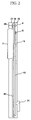
- FIG. 1 shows a plan view of a detection element 1 of the thermal type flow rate measuring apparatus of the first embodiment.
- Fig. 2 shows a cross section taken along line A-A' of the detection element 1 of the thermal type flow rate measuring apparatus of the first embodiment
- Fig. 3 shows a plan view illustrating the layout of the diffusion layer 40 of the detection element 1 of the thermal type flow rate measuring apparatus of the first embodiment
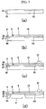
- Fig. 4 shows a process chart for the detection element 1 of the thermal type flow rate measuring apparatus of the first embodiment.
- FIG. 5 shows cross sections illustrating the process steps for the detection element 1 of the thermal type flow rate measuring apparatus of the first embodiment.
- Fig. 6 shows a first drive circuit of the thermal type flow rate measuring apparatus of the first embodiment.
- Fig. 7 shows a second drive circuit of the thermal type flow rate measuring apparatus of the first embodiment
- the structure of the detection element 1 of the present thermal type flow rate measuring apparatus is described with reference to Figs. 1 , 2 , and 3 .
- the detection element 1 includes a planar substrate 37 made of a material having a good heat conductivity, such as silicon, ceramic, and the like. After an insulating film 38 is formed on the substrate 37, the substrate 37 is etched on its back surface to form a space under the insulating film 38, thereby forming a diaphragm (thin-walled part) 2.
- a heat-generating resistor 6 functioning as a heat-generating element that is heated to a predetermined temperature difference from the temperature of the flow of air to be measured; a heat-generating element temperature-detecting resistor 5 disposed near the heat-generating resistor 6 for detecting its temperature; and temperature-detecting resistors 3, 4, 7, and 8 disposed on both sides (upwind and downwind sides) of the heat-generating resistor 6 as temperature-detecting means.
- the heat-generating resistor 6 is a resistor made of polysilicon thin film, platinum thin film, nickel alloy thin film, or the like; it generates heat when electric current flows through it.
- the heat-generating element temperature-detecting resistor 5 and the temperature-detecting resistors 3, 4, 7, and 8 are also resistors made of polysilicon thin film, platinum thin film, nickel alloy thin film, or the like. By taking advantage of the change in the resistance values of these resistors depending on temperature, the temperature of the heat-generating element 6 can be detected with the heat-generating element temperature-detecting resistor 5, and the temperature on both sides (upwind and downwind) of the heat-generating resistor 6 can be detected with the temperature-detecting resistors 3, 4, 7, and 8.
- the heat-generating resistor 6 is connected, via wiring portions 18 and 24, to connecting terminals 31 and 32 for external electrical connection.
- the heat-generating element temperature-detecting resistor 5 is connected, via wiring portions 15 and 16, to connecting terminals 29 and 30 for external electrical connection.
- the temperature-detecting resistors 3, 4, 7, and 8 are connected, via wiring portions 10, 11, 12, 13, 19, 20, 21, and 22, to connecting terminals 25, 26, 27, 28, 33, 34, 35, and 36 for external electrical connection.
- a diffusion layer 40 is provided on the planar substrate 37 except for the areas of the diaphragm 2 and the peripheries of the planar substrate 37, as shown in Fig. 3 , so as to decrease the resistance of the surface portion of the substrate.
- the diffusion layer 40 is electrically connected externally via the terminal 31 by contacts disposed on a wiring pattern 9. Between the wiring portion 18 and the wiring portion 16, a wiring pattern 17 having contacts connecting to the diffusion layer 40 is disposed, thereby providing a shield between the wiring portion 18 and the wiring portion 16.
- a wiring pattern 14 having contacts connecting to the diffusion layer 40 is disposed, thereby providing a shield between the wiring portion 13 and the wiring portion 15.
- a wiring pattern 23 having contacts connecting to the diffusion layer 40 is disposed, thereby providing a shield between the wiring portion 22 and the wiring portion 24.
- the heat-generating resistor 6, the heat-generating element temperature-detecting resistor 5, the temperature-detecting resistors 3, 4, 7, and 8, the wiring portions 10, 11, 12, 13, 15, 16, 18, 19, 20,21,22, and 24, and the wiring patterns 9, 14, 17, and 23 are covered with a protection film 39.
- the planar substrate 37 is a silicon substrate, and the heat-generating element 6, the heat-generating element temperature-detecting resistor 5, and the temperature-detecting resistors 3, 4, 7, and 8 are made of a polysilicon thin film.
- the planar substrate 37 (silicon substrate) is subjected to thermal oxidation, photoetching, and As (arsenic) implantation so as to form a diffusion layer 40 on the planar substrate 37, as shown in Fig. 5(a) .
- SiO 2 and Si 3 N 4 deposition (silicon oxide film and silicon nitride film deposition), photoetching, SiO 2 and Si 3 N 4 etching (silicon oxide film and silicon nitride film etching), poly-Si (polysilicon) deposition, phosphorus process, photoetching, and poly-Si (polysilicon) etching are carried out, so as to form the insulating film 38, the wiring pattern 9, the heat-generating element temperature-detecting resistor 5, the heat-generating resistor 6, and the wiring portion 18, as shown in Fig. 5(b) .
- the diffusion layer 40 is electrically connected, via contacts formed (by SiO 2 and Si 3 N 4 etching) in the insulating film 38, by the wiring pattern 9 (which is formed of polysilicon). Thereafter, SiO 2 and Si 3 N 4 deposition (silicon oxide film and silicon nitride film deposition), photoetching, contact etching, AL (aluminum) deposition, photoetching, and AL (aluminum) etching are carried out, so as to form the protection film 39, the connecting terminal 31, and the like, as shown in Fig. 5(c) . Finally, a back-etch is carried out to form the diaphragm 2 as shown in Fig. 5(d) , thereby completing the detection element 1.
- This drive circuit is composed of the following components: a transistor 42 for driving the heat-generating resistor 6; a fixed resistor 43 connected in series with the heat-generating element temperature-detecting resistor 5; a differential amplifier 45 for amplifying the voltage at the connecting point of the heat-generating element temperature-detecting resistor 5 and the fixed resistor 43 (which voltage varies depending on the temperature of the heat-generating resistor 6 because the resistance value of the heat-generating element temperature-detecting resistor 5 varies as the temperature of the heat-generating resistor 6 changes) in comparison with the voltage of a reference voltage source 44, so as to drive the transistor 42; and a differential amplifier 41 for amplifying the voltage of a bridge circuit consisting of the temperature-detecting resistors 3, 4, 7, and 8.
- the capacitance 46 is the parasitic capacitance between the heat-generating element 6 and the heat-generating element temperature-detecting resistor 5.
- the voltage for driving the heat-generating resistor 6 is coupled via the capacitance 46 to the differential amplifier 45.
- Such coupling by way of the capacitance 46 acts as a positive feedback to the differential amplifier 45 and so adversely affects the stability of the temperature control system of the heat-generating resistor 6.
- the control rate of the heat-generating resistor 6 decreases and so the response characteristics of the flow rate measuring apparatus are adversely affected.
- the heat-generating resistor 6 and the wiring portions 18 and 24 are made of the same material. Further, in order to reduce the heat due to the resistance of the wiring portions 18 and 24, the pattern widths of the wiring portions 18 and 24 are made significantly wider than the width of the heat-generating resistor 6.
- the heat-generating element temperature-detecting resistor 5 and the wiring portions 15 and 16 are also made of the same material. Furthermore, in view of the need to reduce the resistance value of the wiring portions 15 and 16 in order to decrease the sensitivity and error in the heat-generating element temperature-detecting resistor 5, the pattern widths of the wiring portions 15 and 16 are also made very wide. Consequently, the capacitance between the wiring portions 18 and 24 and the wiring portions 15 and 16 would become very large.
- the planar substrate is comprised of an electrically conductive silicon substrate and the silicon substrate is used in a floating manner, the capacitance between the wiring portions 18 and 24 and the wiring portions 15 and 16 is made all the more larger.
- the wiring pattern 17 connected to a constant potential (ground potential) is disposed between the wires 16 and 18 so as to reduce the capacitance between the wiring portions 18 and 24 and the wiring portions 15 and 16.
- the width of the wiring pattern 17 is made greater than the thickness of the planar substrate 37 so as to enhance its shield effect.
- the planar substrate 37 is also provided with the diffusion layer 40, with which the wiring pattern 17 is connected via a plurality of contacts.
- the diffusion layer 40 disposed under the wiring portions 18 and 24 and the wiring portions 15 and 16 also helps enhance the shield effect between the wiring portions 18 and 24 and the wiring portions 15 and 16.
- This drive circuit is composed of the following: a transistor 42 for driving the heat-generating resistor 6; a fixed resistor 43 connected in series with the heat-generating element temperature-detecting resistor 5; a comparator 51 for comparing the voltage at the connection point of the heat-generating element temperature-detecting resistor 5 and the fixed resistor 43 (which voltage varies depending on the temperature of the heat-generating resistor 6 because the resistance value of the heat-generating element temperature-detecting resistor 5 varies as the temperature of the heat-generating resistor 6 changes) with the voltage of the reference voltage source 44; a pulse width modulation circuit 50 for pulse-driving the transistor 42 in accordance with the output of the comparator 51; a pulse generator 49 for applying a pulsed voltage to the bridge circuit consisting of the temperature-detecting resistors 3, 4, 7, and 8; and a differential amplifier 41 for amplifying the output voltage of the bridge circuit.
- Capacitance 46 is the parasitic capacitance between the heat-generating resistor 6 and the heat-generating element temperature-detecting resistor 5; capacitance 47 is the parasitic capacitance between the heat-generating resistor 6 and the temperature-detecting resistor 7; and capacitance 48 is the parasitic capacitance between the temperature-detecting resistor 4 and the heat-generating element temperature-detecting resistor 5.
- the voltage to drive the heat-generating resistor 6 is coupled via the capacitance 46 to the comparator 51.
- Such coupling by way of the capacitance 46 causes noise in the comparator 51 when the heat-generating resistor 6 is driven with a pulsed voltage, thereby destabilizing the temperature control of the heat-generating resistor 6. It is therefore necessary to reduce the value of the capacitance 46.
- the voltage to drive the heat-generating resistor 6 is coupled, via the capacitance 47, to the differential amplifier 41. Such coupling causes noise in the differential amplifier 41 when the heat-generating resistor 6 is driven with a pulsed voltage, thereby causing an error in the flow rate detection signal. Thus, it is necessary to reduce the value of the capacitance 47.
- the capacitance 48 couples the pulsed voltage to drive the temperature-detecting resistors 3, 4, 7, and 8 with the comparator 51. Such coupling by the capacitance 48 produces noise in the comparator 51 and thereby reduces the accuracy of detection of the temperature of the heat-generating resistor 6. Thus, it is also necessary to reduce the value of the capacitance 48.
- the heat-generating resistor 6 and the wiring portions 18 and 24 are made of the same material. In order to reduce the heat produced by the resistance of the wiring portions 18 and 24, the pattern widths of the wiring portions 18 and 24 are made significantly wider than the width of the heat-generating resistor 6.
- the temperature-detecting resistors 3, 4, 7, and 8 and the wiring portions 10, 11, 12, 13, 19, 20, 21, and 22 are also made of the same material.
- the pattern widths of the wiring portions 10, 11, 12, 13, 19, 20, 21, and 22 are made very large.
- the capacitance between the wiring portions 18 and 24 and the wiring portions 10,11,12,13,19,20, 21, and 22 would become very large. Therefore, in the detection element 1 of the present embodiment, the wiring pattern 14 connected to the ground voltage is disposed between the wiring portions 10, 11, 12, and 13 and the wiring portions 15 and 16, so as to reduce the capacitance between the wiring portions 10, 11, 12, and 13 and the wiring portions 15 and 16.
- the wiring pattern 23 which is connected to ground voltage, whereby the capacitance between the wiring portions 19, 20, 21, and 22 and the wiring portions 18 and 24 is reduced.
- the widths of the wiring patterns 14 and 23 are also made greater than the thickness of the planar substrate 37 so as to enhance their shield effect.
- the planar substrate 37 is further provided with the diffusion layer 40, which is connected to the wiring patterns 14 and 23 via a plurality of contacts. In this way, the impedance of the wiring patterns 14 and 23 is reduced, thereby enhancing their shield effect.
- the shield effects are further enhanced by the diffusion layer 40, which is connected to ground potential, disposed under the wiring portions 10, 11, 12, 13,19,20,21,22,15, and 16.
- the planar substrate 37 may be of P type and the diffusion layer 40 may be ofN type and they may be insulated from each other.
- the planar substrate 37 has been described as being provided with the diffusion layer 40.
- the diffusion layer may be dispensed with and the wiring patterns may be directly electrically connected to the planar substrate with contacts disposed on the wiring patterns; such structure is also included in the scope of the invention.
Landscapes
- Physics & Mathematics (AREA)
- Fluid Mechanics (AREA)
- General Physics & Mathematics (AREA)
- Measuring Volume Flow (AREA)
Claims (6)
- Appareil de mesure de débit du type thermique, comprenant :un élément générateur de chaleur (6) à disposer dans l'écoulement d'un fluide, qui génère de la chaleur quand un courant électrique s'écoule à travers celui-ci ;un premier et un second moyen de détection de température (3, 4, 7, 8) disposés sur les deux côtés de l'élément générateur de chaleur (6) le long de l'écoulement du fluide ;une borne de connexion pour élément générateur de chaleur (31, 32) électriquement connectée à l'élément générateur de chaleur (6) ;une première et une seconde borne de connexion pour moyen de détection de température (25-28, 33-36) électriquement connectées au premier et au second moyen de détection de température (3, 4, 7, 8) ;une portion de câblage pour élément générateur de chaleur (18, 24) qui connecte électriquement l'élément générateur de chaleur (6) et la borne de connexion pour élément générateur de chaleur (31, 32) ; etune première et une seconde portion de câblage pour moyen de détection de température (10-13, 19-22) qui connecte électriquement le premier et le second moyen de détection de température (3, 4, 7, 8) et la première et la seconde borne de connexion pour moyen de détection de température (25-28, 33-36), respectivement, dans lequel l'appareil comprend en outre :un motif de câblage (14, 23) disposé entre la portion de câblage pour élément générateur de chaleur (18, 24) et la première et la seconde portion de câblage pour moyen de détection de température (10-13, 19-22), et dans lequel le motif de câblage (14, 23) est maintenu à un potentiel constant,l'appareil étant caractérisé en ce qu'il comprend en outre :un moyen de détection de température pour élément générateur de chaleur (5) disposé à proximité de l'élément générateur de température (6) pour détecter la température de l'élément générateur de chaleur (6) ; une borne de connexion pour moyen de détection de température pour élément générateur de chaleur (29, 30) qui est électriquement connectée au moyen de détection de température pour élément générateur de chaleur (5) ; etune portion de câblage pour moyen de détection de température pour élément générateur de chaleur (15, 16) qui connecte électriquement le moyen de détection de température pour élément générateur de chaleur (5) avec la borne de connexion pour moyen de détection de température pour élément générateur de chaleur (29, 30) ;un motif de câblage (17) disposé entre la portion de câblage pour élément générateur de chaleur (18, 24) et la portion de câblage pour moyen de détection de température pour élément générateur de chaleur (15, 16), dans lequel le motif de câblage (17) est maintenu à un potentiel constant.
- Appareil de mesure de débit du type thermique selon la revendication 1, comprenant :un motif de câblage (9, 14, 17, 23) disposé entre la portion de câblage pour moyen de détection de température pour élément générateur de chaleur (18, 24) et la première et la seconde portion de câblage pour moyen de détection de température (3, 4, 7, 8), dans lequel le motif de câblage (9, 14, 17, 23) est maintenu à un potentiel constant.
- Appareil de mesure de débit du type thermique selon l'une quelconque des revendications 1 et 2, comprenant :une couche en film mince, de laquelle sont faits l'élément générateur de chaleur (6) et la portion de câblage pour élément générateur de chaleur (18, 24) ; etun substrat planaire électriquement conducteur (37) sur lequel la couche en film mince est fixée via une couche isolante ;dans lequel la largeur du motif de câblage (9, 14, 17, 23) est plus grande que l'épaisseur du substrat planaire (37).
- Appareil de mesure de débit du type thermique selon la revendication 3, dans lequel le motif de câblage (9, 14, 17, 23) est connecté électriquement avec le substrat planaire (37).
- Appareil de mesure de débit du type thermique selon la revendication 4, dans lequel le motif de câblage (9, 14, 17, 23) comprend des portions de connexion disposées successivement, qui sont connectées électriquement avec le substrat planaire (37).
- Appareil de mesure de débit du type thermique selon l'une quelconque des revendications 3 à 5, comprenant une couche de diffusion (40) formée sur le substrat planaire (37) de manière à réduire la résistance du substrat planaire (37).
Applications Claiming Priority (1)
| Application Number | Priority Date | Filing Date | Title |
|---|---|---|---|
| JP2006171594A JP4226616B2 (ja) | 2006-06-21 | 2006-06-21 | 熱式流量計測装置 |
Publications (3)
| Publication Number | Publication Date |
|---|---|
| EP1870681A2 EP1870681A2 (fr) | 2007-12-26 |
| EP1870681A3 EP1870681A3 (fr) | 2013-02-27 |
| EP1870681B1 true EP1870681B1 (fr) | 2016-08-24 |
Family
ID=38654807
Family Applications (1)
| Application Number | Title | Priority Date | Filing Date |
|---|---|---|---|
| EP07012215.5A Ceased EP1870681B1 (fr) | 2006-06-21 | 2007-06-21 | Débitmètre thermique |
Country Status (3)
| Country | Link |
|---|---|
| US (1) | US7617723B2 (fr) |
| EP (1) | EP1870681B1 (fr) |
| JP (1) | JP4226616B2 (fr) |
Families Citing this family (7)
| Publication number | Priority date | Publication date | Assignee | Title |
|---|---|---|---|---|
| JP4976469B2 (ja) | 2009-08-28 | 2012-07-18 | 日立オートモティブシステムズ株式会社 | 熱式湿度センサ |
| JP5152292B2 (ja) * | 2010-10-06 | 2013-02-27 | 株式会社デンソー | 流量計測装置 |
| EP3225958B1 (fr) * | 2014-11-28 | 2021-09-01 | Hitachi Automotive Systems, Ltd. | Capteur de débit du type thermique |
| GB2553681B (en) | 2015-01-07 | 2019-06-26 | Homeserve Plc | Flow detection device |
| GB201501935D0 (en) | 2015-02-05 | 2015-03-25 | Tooms Moore Consulting Ltd And Trow Consulting Ltd | Water flow analysis |
| FR3069126B1 (fr) * | 2017-07-12 | 2020-11-13 | Commissariat Energie Atomique | Dispositif de regeneration de composants electroniques en environnement nucleaire |
| US11092101B2 (en) * | 2018-08-22 | 2021-08-17 | Rosemount Aerospace Inc. | Heater in-circuit capacitive measurement |
Family Cites Families (11)
| Publication number | Priority date | Publication date | Assignee | Title |
|---|---|---|---|---|
| JPS6239722A (ja) | 1985-08-16 | 1987-02-20 | Nippon Soken Inc | 流量センサ用膜式抵抗 |
| US5291781A (en) * | 1991-04-12 | 1994-03-08 | Yamatake-Honeywell Co., Ltd. | Diaphragm-type sensor |
| JPH06230021A (ja) * | 1993-02-01 | 1994-08-19 | Ricoh Co Ltd | 感熱式流速計及びこれを用いたフルイディック流量計 |
| US6095084A (en) * | 1996-02-02 | 2000-08-01 | Applied Materials, Inc. | High density plasma process chamber |
| JP3513041B2 (ja) | 1999-01-25 | 2004-03-31 | 三菱電機株式会社 | 流量センサ |
| JP2001176365A (ja) * | 1999-12-15 | 2001-06-29 | Mitsubishi Electric Corp | 圧力スイッチ |
| CN1272606C (zh) * | 2000-07-27 | 2006-08-30 | 株式会社日立制作所 | 热式空气流量计 |
| US6432812B1 (en) * | 2001-07-16 | 2002-08-13 | Lsi Logic Corporation | Method of coupling capacitance reduction |
| DE10324292B4 (de) * | 2003-05-21 | 2018-03-15 | Robert Bosch Gmbh | Messelement für einen Durchflusssensor, insbesondere einen Luftmassensensor für Brennkraftmaschinen |
| JP2004361271A (ja) | 2003-06-05 | 2004-12-24 | Hitachi Ltd | 熱式空気流量計 |
| DE10345584A1 (de) * | 2003-09-29 | 2005-04-28 | Bosch Gmbh Robert | Leiterplatte mit Kunststoffteil zur Aufnahme einer Messeinrichtung |
-
2006
- 2006-06-21 JP JP2006171594A patent/JP4226616B2/ja not_active Expired - Fee Related
-
2007
- 2007-06-20 US US11/765,736 patent/US7617723B2/en not_active Expired - Fee Related
- 2007-06-21 EP EP07012215.5A patent/EP1870681B1/fr not_active Ceased
Also Published As
| Publication number | Publication date |
|---|---|
| US20080016958A1 (en) | 2008-01-24 |
| EP1870681A2 (fr) | 2007-12-26 |
| EP1870681A3 (fr) | 2013-02-27 |
| JP4226616B2 (ja) | 2009-02-18 |
| JP2008002896A (ja) | 2008-01-10 |
| US7617723B2 (en) | 2009-11-17 |
Similar Documents
| Publication | Publication Date | Title |
|---|---|---|
| EP0395721B1 (fr) | Circuits de commande et de detection pour capteurs d'ecoulement massique d'air | |
| KR960015067B1 (ko) | 실리콘 베이스 질량 기류 센서 및 그 조립방법 | |
| EP1870681B1 (fr) | Débitmètre thermique | |
| US8689608B2 (en) | Thermal gas sensor | |
| US6209402B1 (en) | Measuring element, mass air flow meter therewith and compensating method for accurately measuring air flow | |
| US6557411B1 (en) | Heating element type mass air flow sensor, and internal combustion engine-control apparatus using the sensor | |
| EP2280251B1 (fr) | Débitmètre thermique | |
| US9188470B2 (en) | Thermal flow meter | |
| CN101852630B (zh) | 热式流量计 | |
| US4733559A (en) | Thermal fluid flow sensing method and apparatus for sensing flow over a wide range of flow rates | |
| JP4608843B2 (ja) | 流量測定装置 | |
| WO2012043164A1 (fr) | Capteur de débit thermique | |
| JP3758081B2 (ja) | 熱式流量検出装置 | |
| US6725716B1 (en) | Thermo-sensitive flow rate sensor and method of manufacturing the same | |
| JPH10213470A (ja) | 薄膜式抵抗体及びその製造方法、流量センサ、湿度センサ、ガスセンサ、温度センサ | |
| US6684693B2 (en) | Heat generation type flow sensor | |
| US20200284633A1 (en) | Fluid sensor | |
| JP2004347590A (ja) | 流量センサ用測定エレメント | |
| JPH102773A (ja) | 熱式空気流量計 | |
| JP3524707B2 (ja) | マイクロフローセンサ素子 | |
| EP1306655A1 (fr) | Sonde manom trique | |
| JPH1062220A (ja) | 熱式空気流量計 | |
| JP2003106884A (ja) | 気流センサ | |
| JP2005031078A (ja) | センサ素子 | |
| JP2003106883A (ja) | 気流センサ |
Legal Events
| Date | Code | Title | Description |
|---|---|---|---|
| PUAI | Public reference made under article 153(3) epc to a published international application that has entered the european phase |
Free format text: ORIGINAL CODE: 0009012 |
|
| AK | Designated contracting states |
Kind code of ref document: A2 Designated state(s): AT BE BG CH CY CZ DE DK EE ES FI FR GB GR HU IE IS IT LI LT LU LV MC MT NL PL PT RO SE SI SK TR |
|
| AX | Request for extension of the european patent |
Extension state: AL BA HR MK YU |
|
| 17P | Request for examination filed |
Effective date: 20090409 |
|
| PUAL | Search report despatched |
Free format text: ORIGINAL CODE: 0009013 |
|
| AK | Designated contracting states |
Kind code of ref document: A3 Designated state(s): AT BE BG CH CY CZ DE DK EE ES FI FR GB GR HU IE IS IT LI LT LU LV MC MT NL PL PT RO SE SI SK TR |
|
| AX | Request for extension of the european patent |
Extension state: AL BA HR MK RS |
|
| RIC1 | Information provided on ipc code assigned before grant |
Ipc: G01F 1/692 20060101ALI20130123BHEP Ipc: G01F 1/684 20060101AFI20130123BHEP Ipc: G01F 1/698 20060101ALI20130123BHEP |
|
| AKX | Designation fees paid |
Designated state(s): DE |
|
| 17Q | First examination report despatched |
Effective date: 20131028 |
|
| GRAP | Despatch of communication of intention to grant a patent |
Free format text: ORIGINAL CODE: EPIDOSNIGR1 |
|
| INTG | Intention to grant announced |
Effective date: 20160502 |
|
| GRAS | Grant fee paid |
Free format text: ORIGINAL CODE: EPIDOSNIGR3 |
|
| GRAA | (expected) grant |
Free format text: ORIGINAL CODE: 0009210 |
|
| AK | Designated contracting states |
Kind code of ref document: B1 Designated state(s): DE |
|
| RIN1 | Information on inventor provided before grant (corrected) |
Inventor name: HANZAWA, KEIJI Inventor name: NAKANO, HIROSHI Inventor name: MATSUMOTO, MASAHIRO Inventor name: YAMADA, MASAMICHI Inventor name: KANAMARU, YASUHIRO |
|
| REG | Reference to a national code |
Ref country code: DE Ref legal event code: R096 Ref document number: 602007047575 Country of ref document: DE |
|
| REG | Reference to a national code |
Ref country code: DE Ref legal event code: R097 Ref document number: 602007047575 Country of ref document: DE |
|
| PLBE | No opposition filed within time limit |
Free format text: ORIGINAL CODE: 0009261 |
|
| STAA | Information on the status of an ep patent application or granted ep patent |
Free format text: STATUS: NO OPPOSITION FILED WITHIN TIME LIMIT |
|
| 26N | No opposition filed |
Effective date: 20170526 |
|
| PGFP | Annual fee paid to national office [announced via postgrant information from national office to epo] |
Ref country code: DE Payment date: 20200609 Year of fee payment: 14 |
|
| REG | Reference to a national code |
Ref country code: DE Ref legal event code: R119 Ref document number: 602007047575 Country of ref document: DE |
|
| PG25 | Lapsed in a contracting state [announced via postgrant information from national office to epo] |
Ref country code: DE Free format text: LAPSE BECAUSE OF NON-PAYMENT OF DUE FEES Effective date: 20220101 |