EP1867006B1 - Transreflecteur d'ondes millimetriques et systeme pour la generation d'un front d'onde coherent collimate - Google Patents
Transreflecteur d'ondes millimetriques et systeme pour la generation d'un front d'onde coherent collimate Download PDFInfo
- Publication number
- EP1867006B1 EP1867006B1 EP06739064.1A EP06739064A EP1867006B1 EP 1867006 B1 EP1867006 B1 EP 1867006B1 EP 06739064 A EP06739064 A EP 06739064A EP 1867006 B1 EP1867006 B1 EP 1867006B1
- Authority
- EP
- European Patent Office
- Prior art keywords
- transreflector
- millimeter
- wave signal
- rectangles
- incident
- Prior art date
- Legal status (The legal status is an assumption and is not a legal conclusion. Google has not performed a legal analysis and makes no representation as to the accuracy of the status listed.)
- Expired - Lifetime
Links
Images

Classifications
-
- H—ELECTRICITY
- H01—ELECTRIC ELEMENTS
- H01Q—ANTENNAS, i.e. RADIO AERIALS
- H01Q19/00—Combinations of primary active antenna elements and units with secondary devices, e.g. with quasi-optical devices, for giving the antenna a desired directional characteristic
- H01Q19/10—Combinations of primary active antenna elements and units with secondary devices, e.g. with quasi-optical devices, for giving the antenna a desired directional characteristic using reflecting surfaces
- H01Q19/18—Combinations of primary active antenna elements and units with secondary devices, e.g. with quasi-optical devices, for giving the antenna a desired directional characteristic using reflecting surfaces having two or more spaced reflecting surfaces
- H01Q19/19—Combinations of primary active antenna elements and units with secondary devices, e.g. with quasi-optical devices, for giving the antenna a desired directional characteristic using reflecting surfaces having two or more spaced reflecting surfaces comprising one main concave reflecting surface associated with an auxiliary reflecting surface
- H01Q19/195—Combinations of primary active antenna elements and units with secondary devices, e.g. with quasi-optical devices, for giving the antenna a desired directional characteristic using reflecting surfaces having two or more spaced reflecting surfaces comprising one main concave reflecting surface associated with an auxiliary reflecting surface wherein a reflecting surface acts also as a polarisation filter or a polarising device
-
- H—ELECTRICITY
- H01—ELECTRIC ELEMENTS
- H01Q—ANTENNAS, i.e. RADIO AERIALS
- H01Q15/00—Devices for reflection, refraction, diffraction or polarisation of waves radiated from an antenna, e.g. quasi-optical devices
- H01Q15/02—Refracting or diffracting devices, e.g. lens, prism
- H01Q15/12—Refracting or diffracting devices, e.g. lens, prism functioning also as polarisation filter
-
- H—ELECTRICITY
- H01—ELECTRIC ELEMENTS
- H01Q—ANTENNAS, i.e. RADIO AERIALS
- H01Q15/00—Devices for reflection, refraction, diffraction or polarisation of waves radiated from an antenna, e.g. quasi-optical devices
- H01Q15/14—Reflecting surfaces; Equivalent structures
- H01Q15/22—Reflecting surfaces; Equivalent structures functioning also as polarisation filter
-
- H—ELECTRICITY
- H01—ELECTRIC ELEMENTS
- H01Q—ANTENNAS, i.e. RADIO AERIALS
- H01Q3/00—Arrangements for changing or varying the orientation or the shape of the directional pattern of the waves radiated from an antenna or antenna system
- H01Q3/44—Arrangements for changing or varying the orientation or the shape of the directional pattern of the waves radiated from an antenna or antenna system varying the electric or magnetic characteristics of reflecting, refracting, or diffracting devices associated with the radiating element
- H01Q3/46—Active lenses or reflecting arrays
Definitions
- Some embodiments of the present invention pertain to millimeter-wave systems. Some embodiments relate to the generation of coherent energy.
- US patent no. 3,276, 023 discloses an array for reflecting a beam of incident radio frequency energy from a source outside of the confines of said array and changing the phase of the reflected energy with respect to the incident energy comprising a plurality of grid members.
- European patent publication no. EP1120856 relates to a printed circuit technology multilayer planar reflector reflecting the electromagnetic field from a field forming a collimated or conformal beam by performing adjustments in the reflection coefficient phases.
- the invention is directed towards a planar multi-layer transreflector and a system for generating collimated coherent millimetre-wave energy.
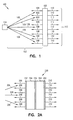
- FIG. 1 is an illustration of a millimeter-wave collimated coherent wavefront generating system in accordance with some embodiments of the present invention.
- Millimeter-wave collimated coherent wavefront generating system 100 may be used for generating collimated coherent millimeter-wave energy and may comprise planar multilayer transreflector 102 and millimeter-wave source 104.
- Millimeter-wave source 104 may be positioned at a focus of transreflector 102 and may provide incident millimeter-wave signal 106.
- Multilayer transreflector 102 may substantially reflect cross-polarized component 108 of incident millimeter-wave signal 106 and may substantially transmit remaining portions 110 of incident millimeter-wave signal 106 to generate collimated coherent millimeter-wave wavefront 112.
- cross-polarized component 108 may be substantially orthogonal to the polarization of incident millimeter-wave signal 106 and may substantially transmit remaining portions 110 of incident millimeter-wave signal 106.
- multilayer transreflector 102 may comprise a plurality of insulating layers arranged between metallic layers.
- the metallic layers each may comprise a plurality of rectangles arranged in a grid pattern that may vary radially within circumferential regions to allow multilayer transreflector 102 to substantially reflect cross-polarized component 108 of incident millimeter-wave signal 106 and to substantially transmit remaining portions 110 of incident millimeter-wave signal 106.
- Remaining portions 110 may include a cross-polarized component as well as a co-polarized component of incident millimeter-wave signal 106. Embodiments of this are described in more detail below.
- embodiments are described herein as substantially reflecting a cross-polarized (i.e., orthogonal) component, the scope of the invention is not limited in this respect.
- Other embodiments of the present invention may reflect a co-polarized component (i.e., having the same polarization) of incident millimeter-wave signal 106 and may transmit the remaining portions.
- source 104 may comprise a microwave or millimeter-wave amplifier array with orthogonally polarized input and output antennas to receive reflected cross-polarized component 108 and transmit co-polarized incident millimeter-wave signal 106. Example embodiments of this are discussed in more detail below. In other embodiments, source 104 may be a microwave or millimeter-wave point source, although the scope of the invention is not limited in this respect.
- FIG. 2A illustrates a side view of a multilayer transreflector in accordance with some embodiments of the present invention.
- FIG. 2B illustrates a top view of a metallic layer of the multilayer transreflector of FIG. 2A including an exploded view of a portion of the metallic layer.
- Multilayer transreflector 200 may be suitable for use as transreflector 102 ( FIG. 1 ) although other transreflectors may also be used.
- Transreflector 200 may comprise one or more insulating layers 204 and metallic layers 202 disposed on the one or more insulating layers 204. This combination may substantially reflect cross-polarized component 208 of incident millimeter-wave signal 206 and may substantially transmit remaining portions 210 of incident millimeter-wave signal 206.
- reflected cross-polarized components 208 may be a substantially collimated and a substantially coherent wavefront.
- transmitted remaining portions 210 may be a substantially collimated and a substantially coherent wavefront.
- metallic layer 202 may comprise a plurality of rectangles 212 arranged in a grid pattern.
- the size of rectangles 212 may radially vary in size within each of circumferential regions 216 (i.e., rings).
- the plurality of rectangles 212 may vary in size radially outward from larger to smaller within each of circumferential regions 216. In some other embodiments, the plurality of rectangles 212 may vary in size radially outward from smaller to larger within each of circumferential regions 216. In some embodiments, rectangles 212 may be squares, although the scope of the invention is not limited in this respect.
- the plurality of rectangles 212 may be electrically coupled by connecting lines 218 in either an x-direction or a y-direction. In some embodiments, connecting lines 218 may provide inductive reflections for polarization along lines 218 and may provide capacitive reflections for polarization orthogonal to lines 218. In this way, remaining portions 210 may be substantially transmitted and cross-polarized component 208 of incident millimeter-wave signal 106 may be substantially reflected. The use of connecting lines 218 in both the x and y directions would inhibit this.
- multilayer transreflector 200 may comprise two metallic layers 202 and one insulating layer 204 between metallic layers 202. In some embodiments, multilayer transreflector 200 may comprise three metallic layers 202 and two insulating layers 204 between metallic layers 202. In some two and three-metallic layer embodiments, each of metallic layers 202 may be substantially identical and/or symmetric. In some other three metallic-layer embodiments, the middle metallic layer may be different than the outer metallic layers. In some two-layer embodiments, the two metallic layers may be different. Differences between metallic layers 202 may include the radial spacing between circumferential regions 216, size and variation of rectangles 212, the spacing between rectangles 212, and/or a width of connecting lines 218.
- the variation between layers 202 may be selected to transmit a substantially collimated and substantially coherent wavefront of remaining portions 210 that may be generated from the incident millimeter-wave signal 206.
- the variation between layers 202 may also be selected to reflect a substantially collimated and substantially coherent wavefront of cross-polarized components 208 that may be generated from the incident millimeter-wave signal 206.
- a radial spacing between circumferential regions 216, size and variation of the rectangles 212, a spacing between rectangles 212, a width of connecting lines 218 and/or a thickness of insulating material 204 may be selected so that the grid pattern of the metallic layers together with the insulating layers may generate substantially collimated and substantially coherent wavefronts of reflected and transmitted polarizations, although the scope of the invention is not limited in this respect.
- transreflector 200 may be illuminated by a millimeter-wave point source 104 ( FIG. 1 ) positioned at a focal point which may be focal distance 103 ( FIG. 1 ) from transreflector 200.
- the focal point may be defined as a location in which the reflected and/or transmitted wavefront is collimated, although the scope of the invention is not limited in this respect.
- transreflector 200 may be substantially circular and the focal distance may be approximately equal to the diameter, although the scope of the invention is not limited in this respect. In other embodiments, transreflector 200 may be square or rectangular in shape, although other shapes are also suitable. In these embodiments, metallic layers 202 may be arranged circularly; however insulating layers 204 may extend beyond the diameter of the metallic layer's area for coupling with structural components of the system.
- incident millimeter-wave signal 206 may be generated by millimeter-wave point source 104 ( FIG. 1 ). In some embodiments, incident millimeter-wave signal 206 may either be right-hand or left-hand circularly polarized, although the scope of the invention is not limited in this respect.
- transreflector 200 may be positioned at 45 degrees with respect to incident millimeter-wave signal 206. In this situation, incident millimeter-wave signal 206 may have a polarization that is substantially 45 degrees with respect to the grid structure of transreflector 200.
- source 104 FIG. 1
- source 104 FIG. 1
- source 104 FIG. 1
- source 104 FIG. 1
- circumferential regions 216 may vary radially from a center based on the relation: k*sqrt (r 2 + f 2 ) in which k is the wave number in radians per unit length, r is the radial distance from the center, and f is a focal distance.
- k is the radian frequency in radians/sec divided by the speed of light.
- the grid pattern of the metallic layers may have a radial dependence and no azimuth dependence.
- the grid pattern may be fixed (i.e., the locations of the centers of the squares may be fixed) while the size of squares may be varied.
- circumferential regions 216 i.e., rings
- circumferential regions 216 may correspond to a particular reflection phase, although the scope of the invention is not limited in this respect.
- insulating layer 204 comprises a microwave dielectric material, such as ceramic, quartz, Duroid, etc., although the scope of the invention is not limited in this respect.
- metallic layer 202 may include conductive material such as copper, gold, silver, aluminum, etc. and alloys thereof.
- each metallic layer 202 may be deposited on one of insulating layers 204 using a process such as electroplating or sputtering. Photolithography, for example, may be used for the patterning of metallic layer 202, although the scope of the invention is not limited in this respect.
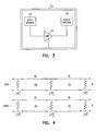
- FIG. 3 illustrates an array element of an amplifier array suitable for use with some embodiments of the present invention.
- the amplifier array may comprise a plurality (e.g., up to several hundred or more) of array elements 302.
- the amplifier array may be suitable for use a source, such as source 104 ( FIG. 1 ) for generating incident millimeter-wave energy for collimation by transreflector 200 ( FIG. 2 ), although the scope of the invention is not limited in this respect as point sources may also be suitable.
- the amplifier array may be referred to as a reflect array.
- the amplifier array may be positioned at or near a focal point of transreflector 200 ( FIG. 2 ) to receive reflected cross-polarized component 208 ( FIG. 2 ).
- Each array element 302 may amplify the received cross-polarized component 208 ( FIG. 2 ) and responsively transmit signals co-polarized signals which are orthogonal to the received cross-polarized component.
- each array element 302 may comprise input antenna 304 having a first polarization to receive reflected cross-polarized component 208 ( FIG. 2 ), millimeter-wave amplifier 306 to amplify the reflected cross-polarized component, and output antenna 308 coupled to an output of amplifier 306.
- output antenna 308 may have a polarization orthogonal to the polarization to input antenna 304 to transmit the signals orthogonal to the received cross-polarized component 208 ( FIG. 2 ).
- the amplifiers of array elements 302 may oscillate at the desired millimeter-wave frequency allowing system 100 to generate wavefront 112 ( FIG. 1 ).
- the amplifier array may receive collimated cross-polarized component 108 ( FIG. 1 ), which may be a coherent wavefront allowing the amplifier array to generate a coherent reflected wavefront comprising co-polarized components.
- the amplifier array may be at least the same size as transreflector 102 ( FIG. 1 ) to receive substantially the entire wavefront of collimated cross-polarized component 108 ( FIG. 1 ).
- output antenna 308 may have the same polarization as input antenna 304, although the scope of the invention is not limited in this respect.
- the pattern of metallic layers 202 may be viewed as aperiodic frequency selective structures (FSSs) in which the grid pattern may vary across the surface in such a way to as to provide a particular reflection and transmission phase at each location on the surface.
- FSSs frequency selective structures
- a desired reflection and transmission phase shift at every point may be produced which modifies the phase front on an incident wave to produce collimation.
- the following analysis may describe the scattering characteristics of the pattern so that it may be designed to produce the desired result.
- transreflector 200 ( FIG. 2 ) is electrically large so that the FSS characteristics change relatively slowly across the transreflector. This may be the case when the ratio of the diameter at the focal distance is close to unity.
- the scattering behavior may be approximated by the behavior of an infinite uniform periodic pattern. This may be repeated for each location across the transreflector.
- the transreflector's grid may be oriented at about 45 degrees with respect to the polarization of the source.
- the incident polarization may be resolved into two orthogonal components (herein referred to as principal axes) that lie along the grid axes.
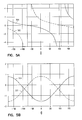
- FIG. 4 shows the equivalent circuits for the structure with each circuit representing scattering in each of the two principal polarizations, referred to as horizontal and vertical polarizations.
- the shunt susceptances are chosen to provide desired reflection and transmission values and may vary across the surface to produce collimation.
- the two outermost layers may be identical. This constraint may simplify the design and may help ensure focusing/collimation for both reflection and transmission simultaneously.
- the four port scattering matrix as seen from the source, which for this analysis is rotated 45 degrees with respect to the transreflector, has the form shown below due to symmetry and reciprocity.
- S S 11 S 12 T 11 T 12 S 12 S 11 T 12 T 11 T 11 T 12 S 11 S 12 T 12 T 11 S 12 S 11
- S 11 should be zero for zero co-polarized reflection and
- ⁇ for a specific cross-polarized reflection.
- the power not reflected may be transmitted through the transreflector as remaining portions 110 ( FIG. 1 ) with a small fraction being absorbed by the losses in the structure.
- Choosing a lower dielectric constant material may result in a narrower range of susceptance values that need to be realized simplifying the design process and possibly providing more robust results.
- values of insulating layer thickness close to a quarter wavelength for each insulating layer seem may provide better results, although the scope of the invention is not limited in this respect.
- a dielectric material with a relative dielectric constant of 2.2 may be used for insulating layers 204 ( FIG. 2 ).
- the electrical thickness of each layer may be assumed to be 90 degrees for simplicity, although this value will change in practice due to the fact that the angle of incidence and the equivalent electrical thickness ⁇ t may vary across the surface.
- a value of ⁇ 0.316 may be chosen to produce 10% reflected power as cross-polarized component 108 ( FIG. 1 ).
- FIGs. 5A and 5B show the values for the four susceptances that produce a given reflection phase ⁇ .
- Reference designation 502 corresponds to susceptance B 1 h
- reference designation 504 corresponds to susceptance B 1 v
- reference designation 506 corresponds to susceptance B 2 h
- reference designation 508 corresponds to susceptance B 2 v in the above equations.
- the example plots illustrated in FIGs. 5A and 5B may be used to design a collimating transreflector in the following way.
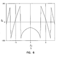
- a source with diameter D o
- the phase of the incident field may be determined at the transreflector's surface.
- phase variation is plotted in FIG. 6 .
- the independent variable in the plot is the radial direction from the transreflector center in wavelengths.
- FSS cells may be designed that produce the desired scattering.
- a suitable electromagnetic code may be used for this purpose, such as Ansoft's HFSS code, or a Method of Moments code.
- a unit cell size is chosen. In practice, smaller unit cells may give more robust results, but a too small cell size may limit the realizable susceptance values. In some embodiments, a unit cell size of ⁇ 0.4 ⁇ may be sufficient.
- the surface may be divided into a grid of unit cells and the average phase of each cell may be given by - ⁇ i ( r ) above. From the phase at each location, the desired susceptances may be determined using the equations above.
- the two outer metallic layers for example, may be designed using the electromagnetic code to provide the desired susceptance values.
- the transreflector comprises one or more of insulating layers between two or more metallic layers.
- the transreflector substantially reflects a cross-polarized component of an incident millimeter-wave signal and substantially transmits remaining portions of the incident millimeter-wave signal.
- the reflected cross-polarized component may be amplified by a reflective array of amplifiers which transmit a co-polarized incident signal.
Landscapes
- Physics & Mathematics (AREA)
- Electromagnetism (AREA)
- Aerials With Secondary Devices (AREA)
- Optical Communication System (AREA)
Claims (5)
- Transflecteur multicouches plan (200) pour générer une énergie cohérente collimatée, comprenant :- une couche isolante (204) ; et- une couche métallique (202) disposée sur la couche isolante (204) afin de réfléchir essentiellement une première partie d'un signal d'onde millimétrique incident (206) et de transmettre essentiellement à travers le transflecteur les parties restantes du signal d'onde millimétrique incident (206) ;- dans lequel la couche métallique (202) comprend plusieurs rectangles (212) disposés en un motif de grille variant radialement en termes de taille dans des régions circonférentielles (216) ;- dans lequel la première partie possède une polarisation essentiellement orthogonale au signal d'onde millimétrique incident ; caractérisé en ce que- les plusieurs rectangles (212) varient en termes de taille radialement vers l'extérieur en allant des plus grands aux plus petits dans chacune des régions circonférentielles (216) ; et- les plusieurs rectangles (212) sont couplés électriquement en connectant des lignes (218) dans une direction x ou dans une direction y afin de réfléchir essentiellement la première partie.
- Transflecteur selon la revendication 1, dans lequel la couche métallique (202) consiste en une de trois couches métalliques (202), et dans lequel la couche isolante (204) consiste en une de deux couches isolantes (204) disposées entre les couches métalliques (202).
- Transflecteur selon la revendication 2, dans lequel la première composante comprend des composantes à polarisation croisée du signal d'onde millimétrique incident (206), et- dans lequel un espacement radial entre les régions circonférentielles (216), une taille et une variation des rectangles (212), un espacement entre les rectangles (212) et une largeur des lignes de connexion (218) sont choisis de manière à générer un front d'onde essentiellement collimaté et essentiellement cohérent (112) des parties restantes (210) du signal d'onde millimétrique incident (206), et à générer un front d'onde essentiellement collimaté et essentiellement cohérent des composantes à polarisation croisée.
- Système (100) pour générer une énergie d'onde millimétrique cohérente collimatée, comprenant :- un transflecteur multicouches plan (102) comprenant plusieurs couches isolantes (204) disposées entre des couches métalliques (202) ; et- une source d'onde millimétrique (104) positionnée au foyer du transflecteur (102) afin de fournir un signal d'onde millimétrique incident (106) ;- dans lequel les couches métalliques (202) comprennent chacune plusieurs rectangles (212) disposés en un motif de grille variant radialement en termes de taille dans des régions circonférentielles (216) afin que le transflecteur multicouches (102) puisse réfléchir essentiellement une première composante du signal d'onde millimétrique incident (206) et transmettre essentiellement les parties restantes (210) du signal d'onde millimétrique incident (206) à travers le transflecteur ; et- dans lequel la première composante possède une polarisation essentiellement orthogonale au signal d'onde millimétrique incident ; caractérisé en ce que- les plusieurs rectangles (212) varient en termes de taille radialement vers l'extérieur dans chacune des régions circonférentielles (216) ; et- les plusieurs rectangles (212) sont couplés électriquement en connectant des lignes (218) dans une direction x ou dans une direction y.
- Système selon la revendication 4, dans lequel la première composante comprend des composantes à polarisation croisée du signal d'onde millimétrique incident (206) ;- dans lequel les parties restantes (210) comprennent un front d'onde essentiellement collimaté et cohérent (110) dans une première direction ;- dans lequel les composantes à polarisation croisée (108) comprennent un front d'onde essentiellement collimaté et cohérent (110) dans une seconde direction ;- dans lequel la couche métallique (202) est une de trois couches métalliques (202) ; et- dans lequel la couche isolante (204) est une de deux couches isolantes (204) disposées entre les couches métalliques (202).
Applications Claiming Priority (2)
| Application Number | Priority Date | Filing Date | Title |
|---|---|---|---|
| US11/100,200 US7304617B2 (en) | 2005-04-05 | 2005-04-05 | Millimeter-wave transreflector and system for generating a collimated coherent wavefront |
| PCT/US2006/010127 WO2006107580A1 (fr) | 2005-04-05 | 2006-03-21 | Transreflecteur d'ondes millimetriques et systeme pour la generation d'un front d'onde coherent collimate |
Publications (2)
| Publication Number | Publication Date |
|---|---|
| EP1867006A1 EP1867006A1 (fr) | 2007-12-19 |
| EP1867006B1 true EP1867006B1 (fr) | 2013-08-14 |
Family
ID=36659821
Family Applications (1)
| Application Number | Title | Priority Date | Filing Date |
|---|---|---|---|
| EP06739064.1A Expired - Lifetime EP1867006B1 (fr) | 2005-04-05 | 2006-03-21 | Transreflecteur d'ondes millimetriques et systeme pour la generation d'un front d'onde coherent collimate |
Country Status (5)
| Country | Link |
|---|---|
| US (2) | US7304617B2 (fr) |
| EP (1) | EP1867006B1 (fr) |
| JP (1) | JP4746090B2 (fr) |
| IL (1) | IL183651A (fr) |
| WO (1) | WO2006107580A1 (fr) |
Families Citing this family (12)
| Publication number | Priority date | Publication date | Assignee | Title |
|---|---|---|---|---|
| TWM320264U (en) * | 2006-12-08 | 2007-10-01 | P Two Ind Inc | Multi-band frequency-selective filter |
| KR100959056B1 (ko) * | 2007-12-10 | 2010-05-20 | 한국전자통신연구원 | 다중 주파수 대역용 주파수 선택 반사기(fss) 구조 |
| JP5250764B2 (ja) * | 2008-09-08 | 2013-07-31 | 株式会社リューテック | レンズアンテナ |
| US8743000B2 (en) * | 2009-07-31 | 2014-06-03 | Her Majesty The Queen In Right Of Canada, As Represented By The Minister Of Industry, Through The Communications Research Centre Canada | Phase element comprising a stack of alternating conductive patterns and dielectric layers providing phase shift through capacitive and inductive couplings |
| US10090603B2 (en) | 2012-05-30 | 2018-10-02 | Wisconsin Alumni Research Foundation | True-time delay, low pass lens |
| DE102013218555A1 (de) * | 2013-07-18 | 2015-01-22 | Rohde & Schwarz Gmbh & Co. Kg | System und Verfahren zur Ausleuchtung und Abbildung eines Objekts |
| US9640867B2 (en) * | 2015-03-30 | 2017-05-02 | Wisconsin Alumni Research Foundation | Tunable spatial phase shifter |
| US10749270B2 (en) | 2018-05-11 | 2020-08-18 | Wisconsin Alumni Research Foundation | Polarization rotating phased array element |
| CN110896314B (zh) * | 2018-09-10 | 2021-07-30 | 深圳市环波科技有限责任公司 | 电磁波信号跨层传输结构及多层电路层 |
| US11239555B2 (en) | 2019-10-08 | 2022-02-01 | Wisconsin Alumni Research Foundation | 2-bit phase quantization phased array element |
| CN116247440B (zh) * | 2023-03-13 | 2025-11-21 | 广西科技大学 | 一种超薄透射/反射双功能超表面天线 |
| CN119209012B (zh) * | 2023-06-27 | 2025-12-09 | 华为技术有限公司 | 一种天线结构和通信装置 |
Family Cites Families (21)
| Publication number | Priority date | Publication date | Assignee | Title |
|---|---|---|---|---|
| US3120856A (en) * | 1960-12-05 | 1964-02-11 | Rehrig Pacific Co | Pressure regulating valve |
| US3267480A (en) | 1961-02-23 | 1966-08-16 | Hazeltine Research Inc | Polarization converter |
| US3276023A (en) * | 1963-05-21 | 1966-09-27 | Dorne And Margolin Inc | Grid array antenna |
| US3972043A (en) * | 1975-02-03 | 1976-07-27 | Northrop Corporation | Cross-polarizing lens reflector |
| IT1180117B (it) * | 1984-11-08 | 1987-09-23 | Cselt Centro Studi Lab Telecom | Struttura per antenna dicroica |
| US4905014A (en) * | 1988-04-05 | 1990-02-27 | Malibu Research Associates, Inc. | Microwave phasing structures for electromagnetically emulating reflective surfaces and focusing elements of selected geometry |
| US5162809A (en) * | 1990-10-23 | 1992-11-10 | Hughes Aircraft Company | Polarization independent frequency selective surface for diplexing two closely spaced frequency bands |
| US5543815A (en) * | 1990-11-30 | 1996-08-06 | Hughes Aircraft Company | Shielding screen for integration of multiple antennas |
| US5214394A (en) * | 1991-04-15 | 1993-05-25 | Rockwell International Corporation | High efficiency bi-directional spatial power combiner amplifier |
| JPH06177639A (ja) * | 1992-12-08 | 1994-06-24 | Nippon Telegr & Teleph Corp <Ntt> | 周波数選択板 |
| GB2328319B (en) * | 1994-06-22 | 1999-06-02 | British Aerospace | A frequency selective surface |
| US6208316B1 (en) * | 1995-10-02 | 2001-03-27 | Matra Marconi Space Uk Limited | Frequency selective surface devices for separating multiple frequencies |
| US5959594A (en) * | 1997-03-04 | 1999-09-28 | Trw Inc. | Dual polarization frequency selective medium for diplexing two close bands at an incident angle |
| US6147572A (en) * | 1998-07-15 | 2000-11-14 | Lucent Technologies, Inc. | Filter including a microstrip antenna and a frequency selective surface |
| ES2153323B1 (es) | 1999-06-07 | 2001-07-16 | Univ Madrid Politecnica | Reflectores planos en tecnologia impresa multicapa y su procedimiento de diseño. |
| JP2002223116A (ja) * | 2001-01-25 | 2002-08-09 | Asahi Glass Co Ltd | 電波収束・偏向体およびアンテナ装置 |
| US6396451B1 (en) * | 2001-05-17 | 2002-05-28 | Trw Inc. | Precision multi-layer grids fabrication technique |
| US6768468B2 (en) * | 2001-09-27 | 2004-07-27 | Raytheon Company | Reflecting surfaces having geometries independent of geometries of wavefronts reflected therefrom |
| US7034751B2 (en) * | 2002-05-20 | 2006-04-25 | Raytheon Company | Reflective and transmissive mode monolithic millimeter wave array system and in-line amplifier using same |
| AU2003247456A1 (en) * | 2003-05-30 | 2005-01-04 | Raytheon Company | Monolithic millmeter wave reflect array system |
| US7526249B2 (en) * | 2004-07-13 | 2009-04-28 | Mediaur Technologies, Inc. | Satellite ground station to receive signals with different polarization modes |
-
2005
- 2005-04-05 US US11/100,200 patent/US7304617B2/en not_active Expired - Lifetime
-
2006
- 2006-03-21 WO PCT/US2006/010127 patent/WO2006107580A1/fr not_active Ceased
- 2006-03-21 JP JP2008505338A patent/JP4746090B2/ja not_active Expired - Fee Related
- 2006-03-21 EP EP06739064.1A patent/EP1867006B1/fr not_active Expired - Lifetime
-
2007
- 2007-06-04 IL IL183651A patent/IL183651A/en not_active IP Right Cessation
- 2007-10-11 US US11/871,042 patent/US7429962B2/en not_active Expired - Lifetime
Also Published As
| Publication number | Publication date |
|---|---|
| WO2006107580A8 (fr) | 2007-02-22 |
| WO2006107580A1 (fr) | 2006-10-12 |
| JP4746090B2 (ja) | 2011-08-10 |
| IL183651A0 (en) | 2007-09-20 |
| JP2008535442A (ja) | 2008-08-28 |
| US20060220973A1 (en) | 2006-10-05 |
| US20080088525A1 (en) | 2008-04-17 |
| US7429962B2 (en) | 2008-09-30 |
| EP1867006A1 (fr) | 2007-12-19 |
| IL183651A (en) | 2010-12-30 |
| US7304617B2 (en) | 2007-12-04 |
Similar Documents
| Publication | Publication Date | Title |
|---|---|---|
| US7429962B2 (en) | Millimeter-wave transreflector and system for generating a collimated coherent wavefront | |
| Guo et al. | Quasi-optical multi-beam antenna technologies for B5G and 6G mmWave and THz networks: A review | |
| Chen et al. | Microwave metalens antennas | |
| Xue et al. | Broadband double-layered Huygens’ metasurface lens antenna for 5G millimeter-wave systems | |
| Song et al. | A high-efficiency conformal transmitarray antenna employing dual-layer ultrathin Huygens element | |
| Ahmed et al. | A near-field meta-steering antenna system with fully metallic metasurfaces | |
| Cai et al. | High-efficiency metasurface with polarization-dependent transmission and reflection properties for both reflectarray and transmitarray | |
| Wu et al. | High-gain filtering reflectarray antenna for millimeter-wave applications | |
| Wu et al. | High-gain dual-band transmitarray | |
| Jiang et al. | Wideband transmit arrays based on anisotropic impedance surfaces for circularly polarized single-feed multibeam generation in the Q-band | |
| Cai et al. | High-performance transmissive meta-surface for $ C $-/$ X $-band lens antenna application | |
| Ang et al. | A passive redirecting Van Atta-type reflector | |
| Lee et al. | Low profile quad‐beam circularly polarised antenna using transmissive metasurface | |
| Bandyopadhyay et al. | Wideband RCS reduction of a linear patch antenna array using AMC metasurface for stealth applications | |
| Lee et al. | Band-switchable substrate-integrated waveguide resonator and filter | |
| Cooper et al. | A novel polarization-independent, free-space, microwave beam splitter utilizing an inkjet-printed, 2-D array frequency selective surface | |
| Song et al. | Two-dimensional wide-angle multibeam flat GRIN lens with a high aperture efficiency | |
| Katare et al. | Anisotropic metasurface-based beam-scanning dual-polarized fan-beam integrated antenna system | |
| Baracco et al. | A dual frequency Ka-band printed Fresnel reflector for ground terminal applications | |
| Wei et al. | Design of compact, broadband, 2-D wide-angle scanning and low-RCS phased array using split ring structures | |
| US11476587B2 (en) | Dielectric reflectarray antenna and method for making the same | |
| Zhong et al. | Broadband low‐profile transmitarray antenna using three‐dimensional cross dipole elements | |
| Xue et al. | An ultrathin and low-profile Huygens meta-lens antenna | |
| Ballandovich et al. | Reflectarray Antenna with Mechanical Beam Steering | |
| Li et al. | A double-layer dual-polarized metasurface transmitarray antenna with low profile |
Legal Events
| Date | Code | Title | Description |
|---|---|---|---|
| PUAI | Public reference made under article 153(3) epc to a published international application that has entered the european phase |
Free format text: ORIGINAL CODE: 0009012 |
|
| 17P | Request for examination filed |
Effective date: 20071017 |
|
| AK | Designated contracting states |
Kind code of ref document: A1 Designated state(s): AT BE BG CH CY CZ DE DK EE ES FI FR GB GR HU IE IS IT LI LT LU LV MC NL PL PT RO SE SI SK TR |
|
| DAX | Request for extension of the european patent (deleted) | ||
| 17Q | First examination report despatched |
Effective date: 20090806 |
|
| REG | Reference to a national code |
Ref country code: DE Ref legal event code: R079 Ref document number: 602006037828 Country of ref document: DE Free format text: PREVIOUS MAIN CLASS: H01Q0019195000 Ipc: H01Q0015120000 |
|
| GRAP | Despatch of communication of intention to grant a patent |
Free format text: ORIGINAL CODE: EPIDOSNIGR1 |
|
| RIC1 | Information provided on ipc code assigned before grant |
Ipc: H01Q 19/195 20060101ALI20130107BHEP Ipc: H01Q 3/46 20060101ALI20130107BHEP Ipc: H01Q 15/12 20060101AFI20130107BHEP Ipc: H01Q 15/22 20060101ALI20130107BHEP |
|
| GRAS | Grant fee paid |
Free format text: ORIGINAL CODE: EPIDOSNIGR3 |
|
| GRAA | (expected) grant |
Free format text: ORIGINAL CODE: 0009210 |
|
| AK | Designated contracting states |
Kind code of ref document: B1 Designated state(s): AT BE BG CH CY CZ DE DK EE ES FI FR GB GR HU IE IS IT LI LT LU LV MC NL PL PT RO SE SI SK TR |
|
| REG | Reference to a national code |
Ref country code: GB Ref legal event code: FG4D |
|
| REG | Reference to a national code |
Ref country code: CH Ref legal event code: EP Ref country code: AT Ref legal event code: REF Ref document number: 627302 Country of ref document: AT Kind code of ref document: T Effective date: 20130815 |
|
| REG | Reference to a national code |
Ref country code: IE Ref legal event code: FG4D |
|
| REG | Reference to a national code |
Ref country code: DE Ref legal event code: R096 Ref document number: 602006037828 Country of ref document: DE Effective date: 20131010 |
|
| REG | Reference to a national code |
Ref country code: NL Ref legal event code: VDEP Effective date: 20130814 Ref country code: AT Ref legal event code: MK05 Ref document number: 627302 Country of ref document: AT Kind code of ref document: T Effective date: 20130814 |
|
| REG | Reference to a national code |
Ref country code: LT Ref legal event code: MG4D |
|
| PG25 | Lapsed in a contracting state [announced via postgrant information from national office to epo] |
Ref country code: CY Free format text: LAPSE BECAUSE OF FAILURE TO SUBMIT A TRANSLATION OF THE DESCRIPTION OR TO PAY THE FEE WITHIN THE PRESCRIBED TIME-LIMIT Effective date: 20130703 Ref country code: AT Free format text: LAPSE BECAUSE OF FAILURE TO SUBMIT A TRANSLATION OF THE DESCRIPTION OR TO PAY THE FEE WITHIN THE PRESCRIBED TIME-LIMIT Effective date: 20130814 Ref country code: PT Free format text: LAPSE BECAUSE OF FAILURE TO SUBMIT A TRANSLATION OF THE DESCRIPTION OR TO PAY THE FEE WITHIN THE PRESCRIBED TIME-LIMIT Effective date: 20131216 Ref country code: IS Free format text: LAPSE BECAUSE OF FAILURE TO SUBMIT A TRANSLATION OF THE DESCRIPTION OR TO PAY THE FEE WITHIN THE PRESCRIBED TIME-LIMIT Effective date: 20131214 Ref country code: LT Free format text: LAPSE BECAUSE OF FAILURE TO SUBMIT A TRANSLATION OF THE DESCRIPTION OR TO PAY THE FEE WITHIN THE PRESCRIBED TIME-LIMIT Effective date: 20130814 Ref country code: SE Free format text: LAPSE BECAUSE OF FAILURE TO SUBMIT A TRANSLATION OF THE DESCRIPTION OR TO PAY THE FEE WITHIN THE PRESCRIBED TIME-LIMIT Effective date: 20130814 |
|
| PG25 | Lapsed in a contracting state [announced via postgrant information from national office to epo] |
Ref country code: GR Free format text: LAPSE BECAUSE OF FAILURE TO SUBMIT A TRANSLATION OF THE DESCRIPTION OR TO PAY THE FEE WITHIN THE PRESCRIBED TIME-LIMIT Effective date: 20131115 Ref country code: FI Free format text: LAPSE BECAUSE OF FAILURE TO SUBMIT A TRANSLATION OF THE DESCRIPTION OR TO PAY THE FEE WITHIN THE PRESCRIBED TIME-LIMIT Effective date: 20130814 Ref country code: BE Free format text: LAPSE BECAUSE OF FAILURE TO SUBMIT A TRANSLATION OF THE DESCRIPTION OR TO PAY THE FEE WITHIN THE PRESCRIBED TIME-LIMIT Effective date: 20130814 Ref country code: LV Free format text: LAPSE BECAUSE OF FAILURE TO SUBMIT A TRANSLATION OF THE DESCRIPTION OR TO PAY THE FEE WITHIN THE PRESCRIBED TIME-LIMIT Effective date: 20130814 Ref country code: SI Free format text: LAPSE BECAUSE OF FAILURE TO SUBMIT A TRANSLATION OF THE DESCRIPTION OR TO PAY THE FEE WITHIN THE PRESCRIBED TIME-LIMIT Effective date: 20130814 Ref country code: PL Free format text: LAPSE BECAUSE OF FAILURE TO SUBMIT A TRANSLATION OF THE DESCRIPTION OR TO PAY THE FEE WITHIN THE PRESCRIBED TIME-LIMIT Effective date: 20130814 |
|
| PG25 | Lapsed in a contracting state [announced via postgrant information from national office to epo] |
Ref country code: CY Free format text: LAPSE BECAUSE OF FAILURE TO SUBMIT A TRANSLATION OF THE DESCRIPTION OR TO PAY THE FEE WITHIN THE PRESCRIBED TIME-LIMIT Effective date: 20130814 |
|
| PG25 | Lapsed in a contracting state [announced via postgrant information from national office to epo] |
Ref country code: CZ Free format text: LAPSE BECAUSE OF FAILURE TO SUBMIT A TRANSLATION OF THE DESCRIPTION OR TO PAY THE FEE WITHIN THE PRESCRIBED TIME-LIMIT Effective date: 20130814 Ref country code: SK Free format text: LAPSE BECAUSE OF FAILURE TO SUBMIT A TRANSLATION OF THE DESCRIPTION OR TO PAY THE FEE WITHIN THE PRESCRIBED TIME-LIMIT Effective date: 20130814 Ref country code: EE Free format text: LAPSE BECAUSE OF FAILURE TO SUBMIT A TRANSLATION OF THE DESCRIPTION OR TO PAY THE FEE WITHIN THE PRESCRIBED TIME-LIMIT Effective date: 20130814 Ref country code: DK Free format text: LAPSE BECAUSE OF FAILURE TO SUBMIT A TRANSLATION OF THE DESCRIPTION OR TO PAY THE FEE WITHIN THE PRESCRIBED TIME-LIMIT Effective date: 20130814 Ref country code: NL Free format text: LAPSE BECAUSE OF FAILURE TO SUBMIT A TRANSLATION OF THE DESCRIPTION OR TO PAY THE FEE WITHIN THE PRESCRIBED TIME-LIMIT Effective date: 20130814 Ref country code: RO Free format text: LAPSE BECAUSE OF FAILURE TO SUBMIT A TRANSLATION OF THE DESCRIPTION OR TO PAY THE FEE WITHIN THE PRESCRIBED TIME-LIMIT Effective date: 20130814 |
|
| PG25 | Lapsed in a contracting state [announced via postgrant information from national office to epo] |
Ref country code: ES Free format text: LAPSE BECAUSE OF FAILURE TO SUBMIT A TRANSLATION OF THE DESCRIPTION OR TO PAY THE FEE WITHIN THE PRESCRIBED TIME-LIMIT Effective date: 20130814 Ref country code: IT Free format text: LAPSE BECAUSE OF FAILURE TO SUBMIT A TRANSLATION OF THE DESCRIPTION OR TO PAY THE FEE WITHIN THE PRESCRIBED TIME-LIMIT Effective date: 20130814 |
|
| PLBE | No opposition filed within time limit |
Free format text: ORIGINAL CODE: 0009261 |
|
| STAA | Information on the status of an ep patent application or granted ep patent |
Free format text: STATUS: NO OPPOSITION FILED WITHIN TIME LIMIT |
|
| 26N | No opposition filed |
Effective date: 20140515 |
|
| REG | Reference to a national code |
Ref country code: DE Ref legal event code: R097 Ref document number: 602006037828 Country of ref document: DE Effective date: 20140515 |
|
| REG | Reference to a national code |
Ref country code: DE Ref legal event code: R119 Ref document number: 602006037828 Country of ref document: DE |
|
| PG25 | Lapsed in a contracting state [announced via postgrant information from national office to epo] |
Ref country code: LU Free format text: LAPSE BECAUSE OF FAILURE TO SUBMIT A TRANSLATION OF THE DESCRIPTION OR TO PAY THE FEE WITHIN THE PRESCRIBED TIME-LIMIT Effective date: 20140321 |
|
| REG | Reference to a national code |
Ref country code: CH Ref legal event code: PL |
|
| REG | Reference to a national code |
Ref country code: IE Ref legal event code: MM4A |
|
| REG | Reference to a national code |
Ref country code: DE Ref legal event code: R119 Ref document number: 602006037828 Country of ref document: DE Effective date: 20141001 |
|
| PG25 | Lapsed in a contracting state [announced via postgrant information from national office to epo] |
Ref country code: DE Free format text: LAPSE BECAUSE OF NON-PAYMENT OF DUE FEES Effective date: 20141001 Ref country code: LI Free format text: LAPSE BECAUSE OF NON-PAYMENT OF DUE FEES Effective date: 20140331 Ref country code: IE Free format text: LAPSE BECAUSE OF NON-PAYMENT OF DUE FEES Effective date: 20140321 Ref country code: CH Free format text: LAPSE BECAUSE OF NON-PAYMENT OF DUE FEES Effective date: 20140331 |
|
| REG | Reference to a national code |
Ref country code: FR Ref legal event code: PLFP Year of fee payment: 11 |
|
| PG25 | Lapsed in a contracting state [announced via postgrant information from national office to epo] |
Ref country code: BG Free format text: LAPSE BECAUSE OF FAILURE TO SUBMIT A TRANSLATION OF THE DESCRIPTION OR TO PAY THE FEE WITHIN THE PRESCRIBED TIME-LIMIT Effective date: 20130814 Ref country code: MC Free format text: LAPSE BECAUSE OF FAILURE TO SUBMIT A TRANSLATION OF THE DESCRIPTION OR TO PAY THE FEE WITHIN THE PRESCRIBED TIME-LIMIT Effective date: 20130814 |
|
| PG25 | Lapsed in a contracting state [announced via postgrant information from national office to epo] |
Ref country code: HU Free format text: LAPSE BECAUSE OF FAILURE TO SUBMIT A TRANSLATION OF THE DESCRIPTION OR TO PAY THE FEE WITHIN THE PRESCRIBED TIME-LIMIT; INVALID AB INITIO Effective date: 20060321 Ref country code: TR Free format text: LAPSE BECAUSE OF FAILURE TO SUBMIT A TRANSLATION OF THE DESCRIPTION OR TO PAY THE FEE WITHIN THE PRESCRIBED TIME-LIMIT Effective date: 20130814 |
|
| REG | Reference to a national code |
Ref country code: FR Ref legal event code: PLFP Year of fee payment: 12 |
|
| REG | Reference to a national code |
Ref country code: FR Ref legal event code: PLFP Year of fee payment: 13 |
|
| PGFP | Annual fee paid to national office [announced via postgrant information from national office to epo] |
Ref country code: GB Payment date: 20200311 Year of fee payment: 15 |
|
| PGFP | Annual fee paid to national office [announced via postgrant information from national office to epo] |
Ref country code: FR Payment date: 20200214 Year of fee payment: 15 |
|
| GBPC | Gb: european patent ceased through non-payment of renewal fee |
Effective date: 20210321 |
|
| PG25 | Lapsed in a contracting state [announced via postgrant information from national office to epo] |
Ref country code: GB Free format text: LAPSE BECAUSE OF NON-PAYMENT OF DUE FEES Effective date: 20210321 Ref country code: FR Free format text: LAPSE BECAUSE OF NON-PAYMENT OF DUE FEES Effective date: 20210331 |