EP1865512A2 - Memory cell programmed using current from access device - Google Patents
Memory cell programmed using current from access device Download PDFInfo
- Publication number
- EP1865512A2 EP1865512A2 EP07011153A EP07011153A EP1865512A2 EP 1865512 A2 EP1865512 A2 EP 1865512A2 EP 07011153 A EP07011153 A EP 07011153A EP 07011153 A EP07011153 A EP 07011153A EP 1865512 A2 EP1865512 A2 EP 1865512A2
- Authority
- EP
- European Patent Office
- Prior art keywords
- phase change
- voltage
- voltage pulse
- state
- change element
- Prior art date
- Legal status (The legal status is an assumption and is not a legal conclusion. Google has not performed a legal analysis and makes no representation as to the accuracy of the status listed.)
- Granted
Links
Images


Classifications
-
- G—PHYSICS
- G11—INFORMATION STORAGE
- G11C—STATIC STORES
- G11C11/00—Digital stores characterised by the use of particular electric or magnetic storage elements; Storage elements therefor
- G11C11/56—Digital stores characterised by the use of particular electric or magnetic storage elements; Storage elements therefor using storage elements with more than two stable states represented by steps, e.g. of voltage, current, phase, frequency
- G11C11/5678—Digital stores characterised by the use of particular electric or magnetic storage elements; Storage elements therefor using storage elements with more than two stable states represented by steps, e.g. of voltage, current, phase, frequency using amorphous/crystalline phase transition storage elements
-
- G—PHYSICS
- G11—INFORMATION STORAGE
- G11C—STATIC STORES
- G11C13/00—Digital stores characterised by the use of storage elements not covered by groups G11C11/00, G11C23/00, or G11C25/00
- G11C13/0002—Digital stores characterised by the use of storage elements not covered by groups G11C11/00, G11C23/00, or G11C25/00 using resistive RAM [RRAM] elements
- G11C13/0004—Digital stores characterised by the use of storage elements not covered by groups G11C11/00, G11C23/00, or G11C25/00 using resistive RAM [RRAM] elements comprising amorphous/crystalline phase transition cells
-
- G—PHYSICS
- G11—INFORMATION STORAGE
- G11C—STATIC STORES
- G11C13/00—Digital stores characterised by the use of storage elements not covered by groups G11C11/00, G11C23/00, or G11C25/00
- G11C13/0002—Digital stores characterised by the use of storage elements not covered by groups G11C11/00, G11C23/00, or G11C25/00 using resistive RAM [RRAM] elements
- G11C13/0021—Auxiliary circuits
- G11C13/0069—Writing or programming circuits or methods
-
- G—PHYSICS
- G11—INFORMATION STORAGE
- G11C—STATIC STORES
- G11C7/00—Arrangements for writing information into, or reading information out from, a digital store
- G11C7/10—Input/output [I/O] data interface arrangements, e.g. I/O data control circuits, I/O data buffers
- G11C7/1078—Data input circuits, e.g. write amplifiers, data input buffers, data input registers, data input level conversion circuits
-
- G—PHYSICS
- G11—INFORMATION STORAGE
- G11C—STATIC STORES
- G11C13/00—Digital stores characterised by the use of storage elements not covered by groups G11C11/00, G11C23/00, or G11C25/00
- G11C13/0002—Digital stores characterised by the use of storage elements not covered by groups G11C11/00, G11C23/00, or G11C25/00 using resistive RAM [RRAM] elements
- G11C13/0021—Auxiliary circuits
- G11C13/0069—Writing or programming circuits or methods
- G11C2013/0071—Write using write potential applied to access device gate
-
- G—PHYSICS
- G11—INFORMATION STORAGE
- G11C—STATIC STORES
- G11C13/00—Digital stores characterised by the use of storage elements not covered by groups G11C11/00, G11C23/00, or G11C25/00
- G11C13/0002—Digital stores characterised by the use of storage elements not covered by groups G11C11/00, G11C23/00, or G11C25/00 using resistive RAM [RRAM] elements
- G11C13/0021—Auxiliary circuits
- G11C13/0069—Writing or programming circuits or methods
- G11C2013/0078—Write using current through the cell
-
- G—PHYSICS
- G11—INFORMATION STORAGE
- G11C—STATIC STORES
- G11C13/00—Digital stores characterised by the use of storage elements not covered by groups G11C11/00, G11C23/00, or G11C25/00
- G11C13/0002—Digital stores characterised by the use of storage elements not covered by groups G11C11/00, G11C23/00, or G11C25/00 using resistive RAM [RRAM] elements
- G11C13/0021—Auxiliary circuits
- G11C13/0069—Writing or programming circuits or methods
- G11C2013/0092—Write characterized by the shape, e.g. form, length, amplitude of the write pulse
-
- G—PHYSICS
- G11—INFORMATION STORAGE
- G11C—STATIC STORES
- G11C2213/00—Indexing scheme relating to G11C13/00 for features not covered by this group
- G11C2213/70—Resistive array aspects
- G11C2213/79—Array wherein the access device being a transistor
Definitions
- Resistive memory utilizes the resistance value of a memory element to store one or more bits of data.
- a memory element programmed to have a high resistance value may represent a logic "1" data bit value
- a memory element programmed to have a low resistance value may represent a logic "0" data bit value.
- the resistance value of the memory element is switched electrically by applying a voltage pulse or a current pulse to the memory element.
- One type of resistive memory is phase change memory. Phase change memory uses a phase change material for the resistive memory element.
- Phase change memories are based on phase change materials that exhibit at least two different states.
- Phase change material may be used in memory cells to store bits of data.
- the states of phase change material may be referred to as amorphous and crystalline states.
- the states may be distinguished because the amorphous state generally exhibits higher resistivity than does the crystalline state.
- the amorphous state involves a more disordered atomic structure, while the crystalline state involves a more ordered lattice.
- Some phase change materials exhibit more than one crystalline state, e.g. a face-centered cubic (FCC) state and a hexagonal closest packing (HCP) state. These two crystalline states have different resistivities and may be used to store bits of data.
- FCC face-centered cubic
- HCP hexagonal closest packing
- Phase change in the phase change materials may be induced reversibly.
- the memory may change from the amorphous state to the crystalline state and from the crystalline state to the amorphous state in response to temperature changes.
- the temperature changes to the phase change material may be achieved in a variety of ways.
- a laser can be directed to the phase change material, current may be driven through the phase change material, or current can be fed through a resistive heater adjacent the phase change material.
- controllable heating of the phase change material causes controllable phase change within the phase change material.
- a phase change memory including a memory array having a plurality of memory cells that are made of phase change material may be programmed to store data utilizing the memory states of the phase change material.
- One way to read and write data in such a phase change memory device is to control a current and/or a voltage pulse that is applied to the phase change material.
- the level of current and/or voltage generally corresponds to the temperature induced within the phase change material in each memory cell.
- a phase change memory cell can store multiple bits of data.
- Multi-bit storage in a phase change memory cell can be achieved by programming the phase change material to have intermediate resistance values or states. Cells in such intermediate states have a resistance that lies between the fully crystalline state and the fully amorphous state. If the phase change memory cell is programmed to one of three different resistance levels, 1.5 bits of data per cell can be stored. If the phase change memory cell is programmed to one of four different resistance levels, two bits of data per cell can be stored, and so on.
- the description in this disclosure is substantially focused on four different resistance levels or states and two bits of data per cell. This is for illustrative purposes only, however, and not intended to limit the scope of the invention. In principle it is possible to store three or more states.
- the amount of crystalline material coexisting with amorphous material and hence the cell resistance is controlled via a suitable write strategy.
- the amount of crystalline material coexisting with amorphous material should be precisely controlled to ensure consistent resistance values for multi-bit storage. Consistent resistance values having a narrow distribution of the different resistance levels ensure that a sufficient sensing margin can be obtained.
- the memory includes a phase change element having a first side and a second side and a first line coupled to the first side of the element.
- the memory includes an access device coupled to the second side of the element and a second line coupled to the access device for controlling the access device.
- the memory includes a circuit for precharging the first line to a first voltage and for applying a voltage pulse to the second line such that a current pulse is generated through the access device to the element to program the element to a selected one of more than two states.
- the voltage pulse has an amplitude based on the selected state.
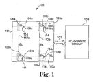
- FIG. 1 is a diagram illustrating one embodiment of a memory device 100.
- Memory device 100 includes memory array 101 and read/write circuit 103.
- Memory array 101 is electrically coupled to read/write circuit 103 through signal path 102.
- Memory array 101 includes a plurality of phase change memory cells 104a-104d (collectively referred to as phase change memory cells 104), a plurality of bit lines (BLs) 112a-112b (collectively referred to as bit lines 112), and a plurality of word lines (WLs) 110a-110b (collectively referred to as word lines 110).
- phase change memory cells 104 phase change memory cells 104
- BLs bit lines
- WLs word lines
- a selected phase change memory cell 104 is programmed by first precharging the bit line 112 coupled to the selected memory cell 104 to a selected or fixed voltage. Next, a voltage pulse is provided on the word line 110 coupled to the selected memory cell 104 to program the selected memory cell 104.
- the bit line precharge voltage and the voltage pulse on the word line form a current through the selected memory cell 104 to program the selected memory cell to a desired resistance state.
- the selected memory cell 104 is programmed to the desired resistance state by controlling the amplitude of the voltage pulse provided on the word line 110. In one embodiment, the precharge voltage applied to the bit line is also adjusted based on the desired resistance state of the selected memory cell 104.
- electrically coupled is not meant to mean that the elements must be directly coupled together and intervening elements may be provided between the “electrically coupled” elements.
- phase change memory cell 104 is electrically coupled to a word line 110, a bit line 112, and a common or ground 114.
- phase change memory cell 104a is electrically coupled to bit line 112a, word line 110a, and common or ground 114
- phase change memory cell 104b is electrically coupled to bit line 112a, word line 110b, and common or ground 114.
- Phase change memory cell 104c is electrically coupled to bit line 112b, word line 110a, and common or ground 114
- phase change memory cell 104d is electrically coupled to bit line 112b, word line 110b, and common or ground 114.
- Each phase change memory cell 104 includes a phase change element 106 and a transistor 108. While transistor 108 is a field-effect transistor (FET) in the illustrated embodiment, in other embodiments, transistor 108 can be another suitable device such as a bipolar transistor or a 3D transistor structure.
- Phase change memory cell 104a includes phase change element 106a and transistor 108a. One side of phase change element 106a is electrically coupled to bit line 112a, and the other side of phase change element 106a is electrically coupled to one side of the source-drain path of transistor 108a. The other side of the source-drain path of transistor 108a is electrically coupled to common or ground 114. The gate of transistor 108a is electrically coupled to word line 110a.
- FET field-effect transistor
- Phase change memory cell 104b includes phase change element 106b and transistor 108b.
- One side of phase change element 106b is electrically coupled to bit line 112a, and the other side of phase change element 106b is electrically coupled to one side of the source-drain path of transistor 108b.
- the other side of the source-drain path of transistor 108b is electrically coupled to common or ground 114.
- the gate of transistor 108b is electrically coupled to word line 110b.
- Phase change memory cell 104c includes phase change element 106c and transistor 108c.
- One side of phase change element 106c is electrically coupled to bit line 112b and the other side of phase change element 106c is electrically coupled to one side of the source-drain path of transistor 108c.
- the other side of the source-drain path of transistor 108c is electrically coupled to common or ground 114.
- the gate of transistor 108c is electrically coupled to word line 110a.
- Phase change memory cell 104d includes phase change element 106d and transistor 108d.
- One side of phase change element 106d is electrically coupled to bit line 112b and the other side of phase change element 106d is electrically coupled to one side of the source-drain path of transistor 108d.
- the other side of the source-drain path of transistor 108d is electrically coupled to common or ground 114.
- the gate of transistor 108d is electrically coupled to word line 110b.
- each phase change element 106 is electrically coupled to a common or ground 114 and each transistor 108 is electrically coupled to a bit line 112.
- phase change memory cell 104a one side of phase change element 106a is electrically coupled to common or ground 114.
- the other side of phase change element 106a is electrically coupled to one side of the source-drain path of transistor 108a.
- the other side of the source-drain path of transistor 108a is electrically coupled to bit line 112a.
- Each phase change element 106 comprises a phase change material that may be made up of a variety of materials in accordance with the present invention.
- chalcogenide alloys that contain one or more elements from group VI of the periodic table are useful as such materials.
- the phase change material of phase change element 106 is made up of a chalcogenide compound material, such as GeSbTe, SbTe, GeTe or AgInSbTe.
- the phase change material is chalcogen free, such as GeSb, GaSb, InSb, or GeGaInSb.
- the phase change material is made up of any suitable material including one or more of the elements Ge, Sb, Te, Ga, As, In, Se, and S.
- Read/write circuit 103 provides signals to memory array 101 through signal path 102 to read data from and write data to memory cells 104. To program memory cells 104, read/write circuit 103 provides a precharge voltage on selected bit lines 112 and provides voltage pulses on selected word lines 110 to form current pulses through selected memory cells 104. The current pulses program one of the more than two resistance levels or states into the phase change material of each of the selected memory cells 104. Read/write circuit 103 senses the state of each memory cell 104 and provides signals that indicate the state of the resistance of each memory cell. Read/write circuit 103 reads each of the more than two states of memory cells 104.
- phase change memory cell 104a During a set operation of phase change memory cell 104a, read/write circuit 103 precharges bit line 112a to a selected or fixed voltage. Next, read/write circuit 103 provides a voltage pulse on word line 110a thereby forming a current pulse through phase change element 106a using transistor 108a. The current pulse heats phase change element 106a above its crystallization temperature (but usually below its melting temperature). In this way, phase change element 106a reaches a crystalline state or a partially crystalline and partially amorphous state during this set operation. The amount of crystalline material coexisting with amorphous material, and hence the resistance of phase change element 106a is controlled by adjusting the amplitude of the voltage pulse provided on word line 110a. In another embodiment, the precharge voltage applied to bit line 112a is also adjusted based on the desired resistance state of phase change element 106a.
- phase change memory cell 104a During a reset operation of phase change memory cell 104a, read/write circuit 103 precharges bit line 112a to a selected or fixed voltage. Next, read/write circuit 103 provides a voltage pulse on word line 110a thereby forming a current pulse through phase change element 106a using transistor 108a. The current pulse quickly heats phase change element 106a above its melting temperature. After the voltage pulse on word line 110a is turned off, phase change element 106a quickly quench cools into the amorphous state or a partially amorphous and partially crystalline state. The amount of amorphous material coexisting with crystalline material, and hence the resistance of phase change element 104a is controlled by adjusting the amplitude of the voltage pulse provided on word line 110a.
- the precharge voltage applied to bit line 112a is also adjusted based on the desired resistance state of phase change element 104a.
- Phase change memory cells 104b-104d and other phase change memory cells 104 in memory array 101 are programmed similarly to phase change memory cell 104a using a similar current pulse formed in response to the bit line and word line voltages.
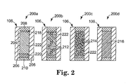
- FIG. 2 is a diagram illustrating one embodiment of a phase change element 106 in four different states at 200a, 200b, 200c, and 200d.
- Phase change element 106 includes a phase change material 204 that is laterally surrounded by insulation material 206.
- Phase change element 106 can have any suitable geometry including phase change material 204 in any suitable geometry and insulation material 206 in any suitable geometry.
- Phase change material 204 is electrically coupled at one end to a first electrode 208 and at the other end to a second electrode 210. Pulses are provided to phase change element 106 via first electrode 208 and second electrode 210. The current path through phase change material 204 is from one of the first electrode 208 and second electrode 210 to the other one of the first electrode 208 and second electrode 210. Phase change element 106 provides a storage location for storing bits of data.
- Insulation material 206 can be any suitable insulator, such as SiO 2 , fluorinated silica glass (FSG), or boro-phosphorous silicate glass (BPSG).
- First electrode 208 and second electrode 210 can be any suitable electrode material, such as TiN, TaN, W, Al, Ti, Ta, TiSiN, TaSiN, TiAIN, TaAlN, or Cu.
- Phase change material 204 is programmed into one of four states to store two bits of data.
- a transistor 108 ( Figure 1) is coupled to first electrode 208 to control the application of pulses to phase change material 204.
- the pulses reset phase change material 204 and program one of the other three states into phase change material 204.
- a small fraction 212 of phase change material 204 has been programmed to change the resistance through phase change material 204 and phase change element 106.
- a medium sized fraction 214 of phase change material 204 has been programmed to change the resistance through phase change material 204 and phase change element 106.
- a large fraction 216 which is substantially all of phase change material 204, has been programmed to change the resistance through phase change material 204 and phase change element 106.
- the size of the programmed fraction is related to the resistance through phase change material 204 and phase change element 106.
- the three different phase change fractions at 200b-200d plus the initial state at 200a provide four states in phase change material 204, and phase change element 106 provides a storage location for storing two bits of data.
- the state of phase change element 106 at 200a is a "00”
- the state of phase change element 106 at 200b is a "01”
- the state of phase change element 106 at 200c is a "10”
- the state of phase change element 106 at 200d is a "11".
- the state of phase change element 106 at 200a is a "11"
- the state of phase change element 106 at 200b is a "10”
- the state of phase change element 106 at 200c is a "01”
- the state of phase change element 106 at 200d is a "00”.
- phase change material 204 is reset to a substantially amorphous state.
- a reset current pulse is provided by a transistor 108 and sent through first electrode 208 and phase change material 204.
- the reset current pulse is formed in response to the precharge voltage on bit line 112 and the voltage pulse provided on word line 110 of transistor 108.
- the reset current pulse heats phase change material 204 above its melting temperature and phase change material 204 is quickly cooled to achieve the substantially amorphous state at 200a.
- phase change material 204 includes crystalline state phase change material at 218 and 220, and amorphous state phase change material at 222.
- the substantially amorphous state at 200a is the highest resistance state of phase change element 106.
- a set current pulse is provided by a transistor 108 and sent through first electrode 208 and phase change material 204.
- the set current pulse is formed in response to the precharge voltage on bit line 112 and the voltage pulse provided on word line 110 of transistor 108.
- transistor 108 provides a set current pulse to program the small volume fraction 212 into a crystalline state.
- the crystalline state is less resistive than the amorphous state and phase change element 106 at 200b has a lower resistance than phase change element 106 in the substantially amorphous state at 200a.
- the partially crystalline and partially amorphous state at 200b is the second highest resistance state of phase change element 106.
- transistor 108 provides a set current pulse to program the medium volume fraction 214 into a crystalline state. Since the crystalline fraction 214 is larger than the crystalline fraction 212 and the crystalline state is less resistive than the amorphous state, phase change element 106 at 200c has a lower resistance than phase change element 106 at 200b and phase change element 106 in the amorphous state at 200a. The partially crystalline and partially amorphous state at 200c is the second lowest resistance state of phase change element 106.
- transistor 108 provides a set current pulse to program substantially all of the phase change material 216 into the crystalline state. Since the crystalline state is less resistive than the amorphous state, phase change element 106 at 200d has a lower resistance than phase change element 106 at 200c, phase change element 106 at 200b, and phase change element 106 in the amorphous state at 200a.
- the substantially crystalline state at 200d is the lowest resistance state of phase change element 106.
- phase change element 106 can be programmed into any suitable number of resistance values or states.
- phase change element 106 can be set to a substantially crystalline state and reset pulses can be used to program phase change element 106 to the desired resistance value or state.
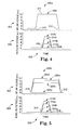
- Figure 3 is a graph 250 illustrating one embodiment of setting the resistance states of a phase change element 106.
- Graph 250 includes the current in Amps (A) applied to the phase change element on x-axis 254 versus the resistance in Ohms of the phase change element on y-axis 252 after applying the specified current.
- a current between approximately 0A and 0.3 x 10 -3 A does not change the resistance state of the phase change element from the fully reset state.
- a current between approximately 0.3 x 10 -3 A and 0.5 x 10 -3 A changes the resistance state of the phase change element to a partially set state as indicated at 260.
- a current between approximately 0.5 x 10 -3 A and 1.4 x 10 -3 A changes the resistance state of the phase change element to a fully set state as indicated at 258.
- a current between approximately 1.4 x 10 -3 A and 1.6 x 10 -3 A changes the resistance state of the phase change element to a partially reset state as indicated at 262.
- a current greater than approximately 1.6 x 10 -3 A changes the resistance state of the phase change element back to the fully reset state as indicated at 256.
- the specific current ranges for obtaining the partially set, fully set, partially reset, and fully reset states will vary based on the phase change material used, the memory cell concept used, and the memory cell dimensions used.
- a phase change element 106 can be programmed to one of four resistance states by controlling the current. If no current is applied, the phase change element remains in the fully reset state. If a small current is applied, the phase change element is programmed to a first state as indicated at 264. This state is illustrated at 200a in Figure 2. In one embodiment, this state is a "11" state. If additional current is applied beyond the first state, the phase change element is programmed to a second state as indicated at 266. This state is illustrated at 200b in Figure 2. In one embodiment, this state is a "10" state. If additional current is applied beyond the second state, the phase change element is programmed to a third state as indicated at 268. This state is illustrated at 200c in Figure 2.
- this state is a "01" state. If additional current is applied beyond the third state, the phase change element is programmed to the fully set state as indicated at 270. This state is illustrated at 200d in Figure 2. In one embodiment, this state is a "00" state.
- a phase change element can also be programmed to one of four resistance states by controlling the current. For example, if a first current is applied, the phase change element is programmed to a first state as indicated at 272. In one embodiment, this state is a "00" state. If additional current is applied beyond the first state, the phase change element is programmed to a second state as indicated at 274. In one embodiment, this state is a "01" state. If additional current is applied beyond the second state, the phase change element is programmed to a third state as indicated at 276. In one embodiment, this state is a "10" state. If additional current is applied beyond the third state, the phase change element is programmed to the fully reset state as indicated at 278. In one embodiment, this state is a "11" state.
- FIG. 4 is a timing diagram 300a illustrating one embodiment of signals for programming a phase change memory cell 104.
- the phase change element 106 begins in the fully reset (i.e., amorphous) state.
- Timing diagram 300a includes time on x-axis 302, bit line voltage on y-axis 304, and word line voltage on y-axis 306.
- read/write circuit 103 precharges the bit line 112 coupled to the selected phase change element 106 as indicated by signal 308.
- Signal 308 increases from 0V at 310 to a fixed voltage at 311 and decreases back to 0V at 312.
- read/write circuit 103 With the bit line precharged to the fixed voltage at 311, read/write circuit 103 provides a selected set voltage pulse on the word line 110 coupled to the gate of the transistor 108, which is coupled to the selected phase change element 106. Each set voltage pulse begins at 316 and ends at 318. Therefore, the selected set voltage pulse defines both the initiation and the termination of the current pulse applied to the selected phase change element 106.
- read/write circuit 103 To program the selected phase change element 106 to the "00" state, such as the state indicated at 200a in Figure 2, read/write circuit 103 provides no set voltage pulse as indicated by signal 314a. To program the selected phase change element 106 to the "01" state, such as the state indicated at 200b in Figure 2, read/write circuit 103 provides a set voltage pulse having a first amplitude as indicated by signal 314b. To program the selected phase change element 106 to the "10" state, such as the state indicated at 200c in Figure 2, read/write circuit 103 provides a set voltage pulse having a second amplitude greater than the first amplitude as indicated by signal 314c. To program the selected phase change element 106 to the "11" state, such as the state indicated at 200d in Figure 2, read/write circuit 103 provides a set voltage pulse having a third amplitude greater than the second amplitude as indicated by signal 314d.
- FIG. 5 is a timing diagram 300b illustrating another embodiment of signals for programming a phase change memory cell 104.
- Timing diagram 300b is similar to timing diagram 300a previously described and illustrated with reference to Figure 4, except that in timing diagram 300b the precharge voltage applied to the bit line 112 also varies based on the desired state of the phase change element 106.
- read/write circuit 103 applies no precharge voltage to the bit line 112 as indicated by signal 320a in addition to providing no set voltage pulse on the word line 110 as indicated by signal 314a.
- read/write circuit 103 applies a first precharge voltage to the bit line 112 as indicated by signal 320b in addition to providing the set voltage pulse indicated by signal 314b.
- read/write circuit 103 applies a second precharge voltage greater than the first precharge voltage to the bit line 112 as indicated by signal 320c in addition to providing the set voltage pulse indicated by signal 314c.
- read/write circuit 103 applies a third precharge voltage greater than the second precharge voltage to the bit line 112 as indicated by signal 320d in addition to providing the set voltage pulse indicated by signal 314d.
- FIG. 6 is a timing diagram 300c illustrating another embodiment of signals for programming a phase change memory cell 104.
- Timing diagram 300c is similar to timing diagram 300a previously described and illustrated with reference to Figure 4, except that timing diagram 300c includes a reset operation.
- Read/write circuit 103 resets the selected phase change element 106 by precharging the bit line 112 as indicated by signal 308.
- Signal 308 increases from 0V at 330 to a fixed voltage at 334 and decreases back to 0V at 332.
- read/write circuit 103 With the bit line 112 precharged to the fixed voltage at 334, read/write circuit 103 provides a voltage pulse on the word line 110 as indicated by signal 340.
- the voltage pulse begins at 336 and ends at 338.
- the amplitude of the reset voltage pulse indicated by signal 340 is greater than the amplitudes of the set pulses indicated by signals 314a-314d.
- the voltage pulse indicated by signal 340 resets the selected phase change element 106 such that one of the subsequent set voltage pulses indicated by signals 314a-314d programs the selected phase change element 106 to the desired state.
- FIG. 7 is a timing diagram 300d illustrating another embodiment of signals for programming a phase change memory cell 104.
- Timing diagram 300d is similar to timing diagram 300c previously described and illustrated with reference to Figure 6, except that in timing diagram 300d the bit line precharge voltage remains applied to the bit line 112 between the reset voltage pulse 340 and the selected set voltage pulse 314a-314d.
- Signal 308 remains at the fixed precharge voltage indicated at 334 and thus the ramp down to 0V at 332 and the ramp up at 310, as illustrated in Figure 6, are skipped.
- FIG 8 is a timing diagram 300e illustrating another embodiment of signals for programming a phase change memory cell 104.
- Timing diagram 300e is similar to timing diagram 300b previously described and illustrated with reference to Figure 5, except that timing diagram 300e includes a reset operation.
- read/write circuit 103 To program a selected phase change element 106 to one of four states, read/write circuit 103 first resets the selected phase change element 106. Read/write circuit 103 resets the selected phase change element 106 by precharging the bit line 112 as indicated by signal 308.
- Signal 308 increases from 0V at 330 to a fixed voltage at 334 and decreases back to 0V at 332.
- read/write circuit 103 With the bit line 112 precharged to the fixed voltage at 334, read/write circuit 103 provides a voltage pulse on the word line 110 as indicated by signal 340.
- the voltage pulse begins at 336 and ends at 338.
- the amplitude of the reset voltage pulse indicated by signal 340 is greater than the amplitudes of the set pulses indicated by signals 314a-314d.
- the voltage pulse indicated by signal 340 resets the selected phase change element 106 such that one of the subsequent set voltage pulses 314a-314d programs the selected phase change element 106 to the desired state.
- FIG 9 is a timing diagram 300f illustrating another embodiment of signals for programming a phase change memory cell 104.
- Timing diagram 300f is similar to timing diagram 300e previously described and illustrated with reference to Figure 8, except that in timing diagram 300f the bit line precharge voltage remains applied to the bit line 112 between the reset voltage pulse 340 and the selected set voltage pulse 314a-314d.
- Signal 308 remains at the fixed precharge voltage indicated at 334 before transitioning to one of the selected precharge voltages indicated at 320a-320d and thus the ramp down to 0V at 332 and the ramp up at 310, as illustrated in Figure 8, are skipped.
- Figure 10 is a timing diagram 300g illustrating another embodiment of signals for programming a phase change memory cell 104.
- a selected phase change element 106 is first programmed to a fully set (i.e., crystalline) state and then reset to the desired state.
- read/write circuit 103 precharges the bit line 112 coupled to the selected phase change element 106 as indicated by signal 308.
- Signal 308 increases from 0V at 330 to a fixed voltage at 334 and decreases back to 0V at 332.
- read/write circuit 103 With the bit line 112 precharged to the fixed voltage at 334, read/write circuit 103 provides a set voltage pulse 352 on the word line 110 coupled to the gate of the transistor 108, which is coupled to the selected phase change element 106.
- the set voltage pulse 352 begins at 354 and ends at 356.
- read/write circuit 103 again precharges bit line 112 as indicated by signal 308.
- Signal 308 increases from 0V at 310 to a fixed voltage at 311 and decreases back to 0V at 312.
- read/write circuit 103 provides a selected reset voltage pulse on the word line 110.
- Each reset voltage pulse begins at 358 and ends at 360. Therefore, the selected reset voltage pulse defines both the initiation and the termination of the current pulse applied to the selected phase change element 106.
- read/write circuit 103 To program the selected phase change element 106 to the "00" state, read/write circuit 103 provides no reset voltage pulse as indicated by signal 350a. To program the selected phase change element 106 to the "01" state, read/write circuit 103 provides a reset voltage pulse having a first amplitude as indicated by signal 350b. To program the selected phase change element 106 to the "10" state, read/write circuit 103 provides a reset voltage pulse having a second amplitude greater than the first amplitude as indicated by signal 350c. To program the selected phase change element 106 to the "11" state, read/write circuit 103 provides a reset voltage pulse having a third amplitude greater than the second amplitude as indicated by signal 350d.
- the amplitude of the set voltage pulse indicated by signal 352 is less than the amplitudes of the reset pulses indicated by signals 350b-350d.
- the voltage pulse indicated by signal 352 sets the selected phase change element 106 such that one of the subsequent reset voltage pulses 350a-350d program the selected phase change element 106 to the desired state.
- FIG 11 is a timing diagram 300h illustrating another embodiment of signals for programming a phase change memory cell 104.
- Timing diagram 300h is similar to timing diagram 300g previously described and illustrated with reference to Figure 10, except that in timing diagram 300h the bit line precharge voltage remains applied to the bit line 112 between the set voltage pulse 352 and the selected reset voltage pulse 350a-350d.
- Signal 308 transitions from the fixed precharge voltage indicated at 334 to the fixed precharge voltage indicated at 311 and thus the ramp down to 0V at 332 and the ramp up at 310, as illustrated in Figure 10, are skipped.
- FIG 12 is a timing diagram 300i illustrating another embodiment of signals for programming a phase change memory cell 104.
- Timing diagram 300i is similar to timing diagram 300g previously described and illustrated with reference to Figure 10, except that in timing diagram 300i the precharge voltage applied to the bit line 112 for the selected reset voltage pulse also varies based on the desired state of the phase change element 106.
- read/write circuit 103 applies no precharge voltage to the bit line 112 as indicated by signal 320a in addition to providing no reset voltage pulse on the word line 110 as indicated by signal 350a.
- read/write circuit 103 applies a first precharge voltage to the bit line 112 as indicated by signal 320b in addition to providing the reset voltage pulse indicated by signal 350b.
- read/write circuit 103 applies a second precharge voltage greater than the first precharge voltage to the bit line 112 as indicated by signal 320c in addition to providing the reset voltage pulse indicated by signal 350c.
- read/write circuit 103 applies a third precharge voltage greater than the second precharge voltage to the bit line 112 as indicated by signal 320d in addition to providing the reset voltage pulse indicated by signal 350d.
- FIG. 13 is a timing diagram 300j illustrating another embodiment of signals for programming a phase change memory cell 104.
- Timing diagram 300j is similar to timing diagram 300i previously described and illustrated with reference to Figure 12, except that in timing diagram 300j the bit line precharge voltage remains applied to the bit line 112 between the set voltage pulse 352 and the selected reset voltage pulse 350a-350d.
- Signal 308 remains at the fixed precharge voltage indicated at 334 before transitioning to one of the selected precharge voltages indicated at 320a-320d and thus the ramp down to 0V at 332 and the ramp up at 310, as illustrated in Figure 12, are skipped.
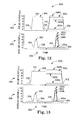
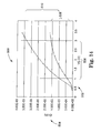
- Figure 14 is a graph 500 illustrating one embodiment of gate voltage versus drain current for high and low bit line precharge voltage ranges.
- Graph 500 includes gate voltage (VG) in Volts (V) on x-axis 502 and drain current (ID) in Amps (A) on y-axis 504.
- VG gate voltage
- ID drain current
- A Amps
- Graph 500 includes gate voltage (VG) in Volts (V) on x-axis 502 and drain current (ID) in Amps (A) on y-axis 504.
- Higher bit line 112 precharge voltages for higher current ranges are indicated at 510, and lower bit line 112 precharge voltages for lower current ranges are indicated at 508.
- One embodiment of a word line 110 voltage range is indicated at 506.
- Curve 512 illustrates gate voltage versus drain current for a first bit line 112 precharge voltage
- curve 514 illustrates gate voltage versus drain current for a second bit line 112 precharge voltage.
- the second bit line 112 precharge voltage is greater than the first bit line 112 precharge voltage.
- the lower bit line 112 precharge voltage indicated at 508 provides better control for low amplitude current pulses as compared to the higher bit line 112 precharge voltage indicated at 510.
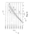
- Figure 15 is a graph 520 illustrating one embodiment of gate voltage versus drain current for varying effective source to drain voltages.
- Graph 520 includes gate voltage (VG) in Volts (V) on x-axis 522 and drain current (ID) in Amps (A) on y-axis 524.
- Curve 530 illustrates gate voltage versus drain current for a drain voltage of 1.5V.
- Curve 532 illustrates gate voltage versus drain current for a drain voltage of 2V.
- Curve 534 illustrates gate voltage versus drain current for a drain voltage of 2.5V, and curve 536 illustrates gate voltage versus drain current for a drain voltage of 3V.
- the dependence of the drain current on the source to drain voltage is small.
- the variation in programming current is insignificant.
- Figure 16 is a chart 550 illustrating one embodiment of the resistance distribution of a phase change element 106 programmed from the reset state into one of four different resistance states.
- Chart 550 includes resistance (R) in Ohms ( ⁇ ) on x-axis 552 and relative frequency on y-axis 554.
- a single 300ns set pulse is applied to the word line 110 with the bit line 112 precharged to program the selected phase change element 106 to the selected state.
- the distribution of resistance values for a phase change element 106 programmed to a "00" state, such as state 200a illustrated in Figure 2, is indicated at 556.
- the distribution of resistance values for a phase change element 106 programmed to a "01" state, such as state 200b illustrated in Figure 2 is indicated at 558.
- the distributions are narrow and separated from each other, such that four distinct resistance levels are reliably achieved.
- Figure 17 is a chart illustrating one embodiment of the resistance distribution of a phase change element 106 programmed from the set state into one of four different resistance states.
- Chart 570 includes resistance (R) in Ohms ( ⁇ ) on x-axis 572 and relative frequency on y-axis 574.
- a single 65ns reset pulse is applied to the word line 110 with the bit line 112 precharged to program the selected phase change element 106 to the selected state.
- the distribution of resistance values for a phase change element 106 programmed to a "00" state is indicated at 576.
- the distribution of resistance values for a phase change element 106 programmed to a "01" state is indicated at 578.
- the distribution of resistance values for a phase change element 106 programmed to a "10" state is indicated at 580, and the distribution of resistance values for a phase change element 106 programmed to a "11” state is indicated at 582.
- the distributions are narrow and separated from each other, such that four distinct resistance levels are reliably achieved.
- Embodiments of the present invention provide a method for programming a phase change memory cell to a selected one of more than two resistance states.
- the memory cells are programmed by first precharging the bit line coupled to the selected memory cell and then by applying a voltage pulse to a word line coupled to the gate of a transistor, which is coupled to the selected memory cell.
- the precharge voltage on the bit line and the voltage pulse on the word line form a current pulse through the selected memory cell using the transistor.
- the current pulse programs the selected memory cell to the desired state.
- the memory cell is set to the desired state.
- the power delivered to the phase change element is precisely controlled.
- no potentially large current source circuits are used, since voltage pulses are applied to the memory cells.
- the pulse timing is not impacted by the resistance-capacitance (R-C) delays of the bit line system.
- the impedance of a word line is independent of the states of the individual phase change memory cells coupled to that word line. Therefore, more reproducible and more uniform pulses can be obtained for programming the phase change elements as compared to typical programming methods.
Abstract
Description
- One type of memory is resistive memory. Resistive memory utilizes the resistance value of a memory element to store one or more bits of data. For example, a memory element programmed to have a high resistance value may represent a logic "1" data bit value, and a memory element programmed to have a low resistance value may represent a logic "0" data bit value. The resistance value of the memory element is switched electrically by applying a voltage pulse or a current pulse to the memory element. One type of resistive memory is phase change memory. Phase change memory uses a phase change material for the resistive memory element.
- Phase change memories are based on phase change materials that exhibit at least two different states. Phase change material may be used in memory cells to store bits of data. The states of phase change material may be referred to as amorphous and crystalline states. The states may be distinguished because the amorphous state generally exhibits higher resistivity than does the crystalline state. Generally, the amorphous state involves a more disordered atomic structure, while the crystalline state involves a more ordered lattice. Some phase change materials exhibit more than one crystalline state, e.g. a face-centered cubic (FCC) state and a hexagonal closest packing (HCP) state. These two crystalline states have different resistivities and may be used to store bits of data.
- Phase change in the phase change materials may be induced reversibly. In this way, the memory may change from the amorphous state to the crystalline state and from the crystalline state to the amorphous state in response to temperature changes. The temperature changes to the phase change material may be achieved in a variety of ways. For example, a laser can be directed to the phase change material, current may be driven through the phase change material, or current can be fed through a resistive heater adjacent the phase change material. In any of these methods, controllable heating of the phase change material causes controllable phase change within the phase change material.
- A phase change memory including a memory array having a plurality of memory cells that are made of phase change material may be programmed to store data utilizing the memory states of the phase change material. One way to read and write data in such a phase change memory device is to control a current and/or a voltage pulse that is applied to the phase change material. The level of current and/or voltage generally corresponds to the temperature induced within the phase change material in each memory cell.
- To achieve higher density phase change memories, a phase change memory cell can store multiple bits of data. Multi-bit storage in a phase change memory cell can be achieved by programming the phase change material to have intermediate resistance values or states. Cells in such intermediate states have a resistance that lies between the fully crystalline state and the fully amorphous state. If the phase change memory cell is programmed to one of three different resistance levels, 1.5 bits of data per cell can be stored. If the phase change memory cell is programmed to one of four different resistance levels, two bits of data per cell can be stored, and so on. For simplicity, the description in this disclosure is substantially focused on four different resistance levels or states and two bits of data per cell. This is for illustrative purposes only, however, and not intended to limit the scope of the invention. In principle it is possible to store three or more states.
- To program a phase change memory cell to an intermediate resistance value, the amount of crystalline material coexisting with amorphous material and hence the cell resistance is controlled via a suitable write strategy. The amount of crystalline material coexisting with amorphous material should be precisely controlled to ensure consistent resistance values for multi-bit storage. Consistent resistance values having a narrow distribution of the different resistance levels ensure that a sufficient sensing margin can be obtained.
- For these and other reasons, there is a need for the present invention.
- One embodiment of the present invention provides a memory. The memory includes a phase change element having a first side and a second side and a first line coupled to the first side of the element. The memory includes an access device coupled to the second side of the element and a second line coupled to the access device for controlling the access device. The memory includes a circuit for precharging the first line to a first voltage and for applying a voltage pulse to the second line such that a current pulse is generated through the access device to the element to program the element to a selected one of more than two states. The voltage pulse has an amplitude based on the selected state.
- The accompanying drawings are included to provide a further understanding of the present invention and are incorporated in and constitute a part of this specification. The drawings illustrate the embodiments of the present invention and together with the description serve to explain the principles of the invention. Other embodiments of the present invention and many of the intended advantages of the present invention will be readily appreciated as they become better understood by reference to the following detailed description. The elements of the drawings are not necessarily to scale relative to each other. Like reference numerals designate corresponding similar parts.
- Figure 1 is a diagram illustrating one embodiment of a memory device.
- Figure 2 is a diagram illustrating one embodiment of a phase change element in four different states.
- Figure 3 is a graph illustrating one embodiment of setting the resistance states of a phase change element.
- Figure 4 is a timing diagram illustrating one embodiment of signals for programming a phase change memory cell.
- Figure 5 is a timing diagram illustrating another embodiment of signals for programming a phase change memory cell.
- Figure 6 is a timing diagram illustrating another embodiment of signals for programming a phase change memory cell.
- Figure 7 is a timing diagram illustrating another embodiment of signals for programming a phase change memory cell.
- Figure 8 is a timing diagram illustrating another embodiment of signals for programming a phase change memory cell.
- Figure 9 is a timing diagram illustrating another embodiment of signals for programming a phase change memory cell.
- Figure 10 is a timing diagram illustrating another embodiment of signals for programming a phase change memory cell.
- Figure 11 is a timing diagram illustrating another embodiment of signals for programming a phase change memory cell.
- Figure 12 is a timing diagram illustrating another embodiment of signals for programming a phase change memory cell.
- Figure 13 is a timing diagram illustrating another embodiment of signals for programming a phase change memory cell.
- Figure 14 is a graph illustrating one embodiment of gate voltage versus drain current for high and low bit line precharge voltage ranges.
- Figure 15 is a graph illustrating one embodiment of gate voltage versus drain current for varying effective source to drain voltages.
- Figure 16 is a chart illustrating one embodiment of the resistance distribution of a phase change element programmed from the reset state into one of four different resistance states.
- Figure 17 is a chart illustrating one embodiment of the resistance distribution of a phase change element programmed from the set state into one of four different resistance states.
- In the following Detailed Description, reference is made to the accompanying drawings, which form a part hereof, and in which is shown by way of illustration specific embodiments in which the invention may be practiced. In this regard, directional terminology, such as "top," "bottom," "front," "back," "leading," "trailing," etc., is used with reference to the orientation of the Figure(s) being described. Because components of embodiments of the present invention can be positioned in a number of different orientations, the directional terminology is used for purposes of illustration and is in no way limiting. It is to be understood that other embodiments may be utilized and structural or logical changes may be made without departing from the scope of the present invention. The following detailed description, therefore, is not to be taken in a limiting sense, and the scope of the present invention is defined by the appended claims.
- Figure 1 is a diagram illustrating one embodiment of a
memory device 100.Memory device 100 includesmemory array 101 and read/write circuit 103.Memory array 101 is electrically coupled to read/write circuit 103 throughsignal path 102.Memory array 101 includes a plurality of phasechange memory cells 104a-104d (collectively referred to as phase change memory cells 104), a plurality of bit lines (BLs) 112a-112b (collectively referred to as bit lines 112), and a plurality of word lines (WLs) 110a-110b (collectively referred to as word lines 110). - A selected phase
change memory cell 104 is programmed by first precharging the bit line 112 coupled to the selectedmemory cell 104 to a selected or fixed voltage. Next, a voltage pulse is provided on the word line 110 coupled to the selectedmemory cell 104 to program the selectedmemory cell 104. The bit line precharge voltage and the voltage pulse on the word line form a current through the selectedmemory cell 104 to program the selected memory cell to a desired resistance state. The selectedmemory cell 104 is programmed to the desired resistance state by controlling the amplitude of the voltage pulse provided on the word line 110. In one embodiment, the precharge voltage applied to the bit line is also adjusted based on the desired resistance state of the selectedmemory cell 104. - As used herein, the term "electrically coupled" is not meant to mean that the elements must be directly coupled together and intervening elements may be provided between the "electrically coupled" elements.
- Each phase
change memory cell 104 is electrically coupled to a word line 110, a bit line 112, and a common orground 114. For example, phasechange memory cell 104a is electrically coupled tobit line 112a,word line 110a, and common orground 114, and phasechange memory cell 104b is electrically coupled tobit line 112a,word line 110b, and common orground 114. Phasechange memory cell 104c is electrically coupled tobit line 112b,word line 110a, and common orground 114, and phasechange memory cell 104d is electrically coupled tobit line 112b,word line 110b, and common orground 114. - Each phase
change memory cell 104 includes aphase change element 106 and a transistor 108. While transistor 108 is a field-effect transistor (FET) in the illustrated embodiment, in other embodiments, transistor 108 can be another suitable device such as a bipolar transistor or a 3D transistor structure. Phasechange memory cell 104a includesphase change element 106a andtransistor 108a. One side ofphase change element 106a is electrically coupled tobit line 112a, and the other side ofphase change element 106a is electrically coupled to one side of the source-drain path oftransistor 108a. The other side of the source-drain path oftransistor 108a is electrically coupled to common orground 114. The gate oftransistor 108a is electrically coupled toword line 110a. - Phase
change memory cell 104b includesphase change element 106b andtransistor 108b. One side ofphase change element 106b is electrically coupled tobit line 112a, and the other side ofphase change element 106b is electrically coupled to one side of the source-drain path oftransistor 108b. The other side of the source-drain path oftransistor 108b is electrically coupled to common orground 114. The gate oftransistor 108b is electrically coupled toword line 110b. - Phase
change memory cell 104c includesphase change element 106c andtransistor 108c. One side ofphase change element 106c is electrically coupled tobit line 112b and the other side ofphase change element 106c is electrically coupled to one side of the source-drain path oftransistor 108c. The other side of the source-drain path oftransistor 108c is electrically coupled to common orground 114. The gate oftransistor 108c is electrically coupled toword line 110a. - Phase
change memory cell 104d includesphase change element 106d andtransistor 108d. One side ofphase change element 106d is electrically coupled tobit line 112b and the other side ofphase change element 106d is electrically coupled to one side of the source-drain path oftransistor 108d. The other side of the source-drain path oftransistor 108d is electrically coupled to common orground 114. The gate oftransistor 108d is electrically coupled toword line 110b. - In another embodiment, each
phase change element 106 is electrically coupled to a common orground 114 and each transistor 108 is electrically coupled to a bit line 112. For example, for phasechange memory cell 104a, one side ofphase change element 106a is electrically coupled to common orground 114. The other side ofphase change element 106a is electrically coupled to one side of the source-drain path oftransistor 108a. The other side of the source-drain path oftransistor 108a is electrically coupled tobit line 112a. - Each
phase change element 106 comprises a phase change material that may be made up of a variety of materials in accordance with the present invention. Generally, chalcogenide alloys that contain one or more elements from group VI of the periodic table are useful as such materials. In one embodiment, the phase change material ofphase change element 106 is made up of a chalcogenide compound material, such as GeSbTe, SbTe, GeTe or AgInSbTe. In another embodiment, the phase change material is chalcogen free, such as GeSb, GaSb, InSb, or GeGaInSb. In other embodiments, the phase change material is made up of any suitable material including one or more of the elements Ge, Sb, Te, Ga, As, In, Se, and S. - Read/
write circuit 103 provides signals tomemory array 101 throughsignal path 102 to read data from and write data tomemory cells 104. Toprogram memory cells 104, read/write circuit 103 provides a precharge voltage on selected bit lines 112 and provides voltage pulses on selected word lines 110 to form current pulses through selectedmemory cells 104. The current pulses program one of the more than two resistance levels or states into the phase change material of each of the selectedmemory cells 104. Read/write circuit 103 senses the state of eachmemory cell 104 and provides signals that indicate the state of the resistance of each memory cell. Read/write circuit 103 reads each of the more than two states ofmemory cells 104. - During a set operation of phase
change memory cell 104a, read/write circuit 103 precharges bitline 112a to a selected or fixed voltage. Next, read/write circuit 103 provides a voltage pulse onword line 110a thereby forming a current pulse throughphase change element 106a usingtransistor 108a. The current pulse heatsphase change element 106a above its crystallization temperature (but usually below its melting temperature). In this way,phase change element 106a reaches a crystalline state or a partially crystalline and partially amorphous state during this set operation. The amount of crystalline material coexisting with amorphous material, and hence the resistance ofphase change element 106a is controlled by adjusting the amplitude of the voltage pulse provided onword line 110a. In another embodiment, the precharge voltage applied tobit line 112a is also adjusted based on the desired resistance state ofphase change element 106a. - During a reset operation of phase
change memory cell 104a, read/write circuit 103 precharges bitline 112a to a selected or fixed voltage. Next, read/write circuit 103 provides a voltage pulse onword line 110a thereby forming a current pulse throughphase change element 106a usingtransistor 108a. The current pulse quickly heatsphase change element 106a above its melting temperature. After the voltage pulse onword line 110a is turned off,phase change element 106a quickly quench cools into the amorphous state or a partially amorphous and partially crystalline state. The amount of amorphous material coexisting with crystalline material, and hence the resistance ofphase change element 104a is controlled by adjusting the amplitude of the voltage pulse provided onword line 110a. In another embodiment, the precharge voltage applied tobit line 112a is also adjusted based on the desired resistance state ofphase change element 104a. Phasechange memory cells 104b-104d and other phasechange memory cells 104 inmemory array 101 are programmed similarly to phasechange memory cell 104a using a similar current pulse formed in response to the bit line and word line voltages. - Figure 2 is a diagram illustrating one embodiment of a
phase change element 106 in four different states at 200a, 200b, 200c, and 200d.Phase change element 106 includes aphase change material 204 that is laterally surrounded byinsulation material 206.Phase change element 106 can have any suitable geometry includingphase change material 204 in any suitable geometry andinsulation material 206 in any suitable geometry. -
Phase change material 204 is electrically coupled at one end to afirst electrode 208 and at the other end to asecond electrode 210. Pulses are provided to phasechange element 106 viafirst electrode 208 andsecond electrode 210. The current path throughphase change material 204 is from one of thefirst electrode 208 andsecond electrode 210 to the other one of thefirst electrode 208 andsecond electrode 210.Phase change element 106 provides a storage location for storing bits of data. -
Insulation material 206 can be any suitable insulator, such as SiO2, fluorinated silica glass (FSG), or boro-phosphorous silicate glass (BPSG).First electrode 208 andsecond electrode 210 can be any suitable electrode material, such as TiN, TaN, W, Al, Ti, Ta, TiSiN, TaSiN, TiAIN, TaAlN, or Cu. -
Phase change material 204 is programmed into one of four states to store two bits of data. A transistor 108 (Figure 1) is coupled tofirst electrode 208 to control the application of pulses to phasechange material 204. The pulses resetphase change material 204 and program one of the other three states intophase change material 204. At 200b, asmall fraction 212 ofphase change material 204 has been programmed to change the resistance throughphase change material 204 andphase change element 106. At 200c, a mediumsized fraction 214 ofphase change material 204 has been programmed to change the resistance throughphase change material 204 andphase change element 106. At 200d, alarge fraction 216, which is substantially all ofphase change material 204, has been programmed to change the resistance throughphase change material 204 andphase change element 106. - The size of the programmed fraction is related to the resistance through
phase change material 204 andphase change element 106. The three different phase change fractions at 200b-200d plus the initial state at 200a provide four states inphase change material 204, andphase change element 106 provides a storage location for storing two bits of data. In one embodiment, the state ofphase change element 106 at 200a is a "00", the state ofphase change element 106 at 200b is a "01", the state ofphase change element 106 at 200c is a "10", and the state ofphase change element 106 at 200d is a "11". In another embodiment, the state ofphase change element 106 at 200a is a "11", the state ofphase change element 106 at 200b is a "10", the state ofphase change element 106 at 200c is a "01", and the state ofphase change element 106 at 200d is a "00". - At 200a,
phase change material 204 is reset to a substantially amorphous state. During a reset operation ofphase change element 106, a reset current pulse is provided by a transistor 108 and sent throughfirst electrode 208 andphase change material 204. The reset current pulse is formed in response to the precharge voltage on bit line 112 and the voltage pulse provided on word line 110 of transistor 108. The reset current pulse heatsphase change material 204 above its melting temperature andphase change material 204 is quickly cooled to achieve the substantially amorphous state at 200a. After a reset operation,phase change material 204 includes crystalline state phase change material at 218 and 220, and amorphous state phase change material at 222. The substantially amorphous state at 200a is the highest resistance state ofphase change element 106. - To program
phase change material 204 into one of the other threestates 200b-200d, a set current pulse is provided by a transistor 108 and sent throughfirst electrode 208 andphase change material 204. The set current pulse is formed in response to the precharge voltage on bit line 112 and the voltage pulse provided on word line 110 of transistor 108. At 200b, transistor 108 provides a set current pulse to program thesmall volume fraction 212 into a crystalline state. The crystalline state is less resistive than the amorphous state andphase change element 106 at 200b has a lower resistance thanphase change element 106 in the substantially amorphous state at 200a. The partially crystalline and partially amorphous state at 200b is the second highest resistance state ofphase change element 106. - At 200c, transistor 108 provides a set current pulse to program the
medium volume fraction 214 into a crystalline state. Since thecrystalline fraction 214 is larger than thecrystalline fraction 212 and the crystalline state is less resistive than the amorphous state,phase change element 106 at 200c has a lower resistance thanphase change element 106 at 200b andphase change element 106 in the amorphous state at 200a. The partially crystalline and partially amorphous state at 200c is the second lowest resistance state ofphase change element 106. - At 200d, transistor 108 provides a set current pulse to program substantially all of the
phase change material 216 into the crystalline state. Since the crystalline state is less resistive than the amorphous state,phase change element 106 at 200d has a lower resistance thanphase change element 106 at 200c,phase change element 106 at 200b, andphase change element 106 in the amorphous state at 200a. The substantially crystalline state at 200d is the lowest resistance state ofphase change element 106. In other embodiments,phase change element 106 can be programmed into any suitable number of resistance values or states. In other embodiments,phase change element 106 can be set to a substantially crystalline state and reset pulses can be used to programphase change element 106 to the desired resistance value or state. - Figure 3 is a
graph 250 illustrating one embodiment of setting the resistance states of aphase change element 106.Graph 250 includes the current in Amps (A) applied to the phase change element onx-axis 254 versus the resistance in Ohms of the phase change element on y-axis 252 after applying the specified current. Starting from a fully reset phase change element as indicated at 256, a current between approximately 0A and 0.3 x 10⁻³A does not change the resistance state of the phase change element from the fully reset state. A current between approximately 0.3 x 10⁻³A and 0.5 x 10⁻³A changes the resistance state of the phase change element to a partially set state as indicated at 260. A current between approximately 0.5 x 10⁻³A and 1.4 x 10⁻³A changes the resistance state of the phase change element to a fully set state as indicated at 258. A current between approximately 1.4 x 10⁻³A and 1.6 x 10⁻³ A changes the resistance state of the phase change element to a partially reset state as indicated at 262. A current greater than approximately 1.6 x 10⁻³A changes the resistance state of the phase change element back to the fully reset state as indicated at 256. The specific current ranges for obtaining the partially set, fully set, partially reset, and fully reset states will vary based on the phase change material used, the memory cell concept used, and the memory cell dimensions used. - Starting from the fully reset state as indicated at 256, a
phase change element 106 can be programmed to one of four resistance states by controlling the current. If no current is applied, the phase change element remains in the fully reset state. If a small current is applied, the phase change element is programmed to a first state as indicated at 264. This state is illustrated at 200a in Figure 2. In one embodiment, this state is a "11" state. If additional current is applied beyond the first state, the phase change element is programmed to a second state as indicated at 266. This state is illustrated at 200b in Figure 2. In one embodiment, this state is a "10" state. If additional current is applied beyond the second state, the phase change element is programmed to a third state as indicated at 268. This state is illustrated at 200c in Figure 2. In one embodiment, this state is a "01" state. If additional current is applied beyond the third state, the phase change element is programmed to the fully set state as indicated at 270. This state is illustrated at 200d in Figure 2. In one embodiment, this state is a "00" state. - Starting from the fully set state as indicated at 258, a phase change element can also be programmed to one of four resistance states by controlling the current. For example, if a first current is applied, the phase change element is programmed to a first state as indicated at 272. In one embodiment, this state is a "00" state. If additional current is applied beyond the first state, the phase change element is programmed to a second state as indicated at 274. In one embodiment, this state is a "01" state. If additional current is applied beyond the second state, the phase change element is programmed to a third state as indicated at 276. In one embodiment, this state is a "10" state. If additional current is applied beyond the third state, the phase change element is programmed to the fully reset state as indicated at 278. In one embodiment, this state is a "11" state.
- Figure 4 is a timing diagram 300a illustrating one embodiment of signals for programming a phase
change memory cell 104. In this embodiment, thephase change element 106 begins in the fully reset (i.e., amorphous) state. Timing diagram 300a includes time onx-axis 302, bit line voltage on y-axis 304, and word line voltage on y-axis 306. To program a selectedphase change element 106 to one of four resistance states, read/write circuit 103 precharges the bit line 112 coupled to the selectedphase change element 106 as indicated bysignal 308.Signal 308 increases from 0V at 310 to a fixed voltage at 311 and decreases back to 0V at 312. With the bit line precharged to the fixed voltage at 311, read/write circuit 103 provides a selected set voltage pulse on the word line 110 coupled to the gate of the transistor 108, which is coupled to the selectedphase change element 106. Each set voltage pulse begins at 316 and ends at 318. Therefore, the selected set voltage pulse defines both the initiation and the termination of the current pulse applied to the selectedphase change element 106. - To program the selected
phase change element 106 to the "00" state, such as the state indicated at 200a in Figure 2, read/write circuit 103 provides no set voltage pulse as indicated bysignal 314a. To program the selectedphase change element 106 to the "01" state, such as the state indicated at 200b in Figure 2, read/write circuit 103 provides a set voltage pulse having a first amplitude as indicated bysignal 314b. To program the selectedphase change element 106 to the "10" state, such as the state indicated at 200c in Figure 2, read/write circuit 103 provides a set voltage pulse having a second amplitude greater than the first amplitude as indicated bysignal 314c. To program the selectedphase change element 106 to the "11" state, such as the state indicated at 200d in Figure 2, read/write circuit 103 provides a set voltage pulse having a third amplitude greater than the second amplitude as indicated bysignal 314d. - Figure 5 is a timing diagram 300b illustrating another embodiment of signals for programming a phase
change memory cell 104. Timing diagram 300b is similar to timing diagram 300a previously described and illustrated with reference to Figure 4, except that in timing diagram 300b the precharge voltage applied to the bit line 112 also varies based on the desired state of thephase change element 106. - To program the selected
phase change element 106 to the "00" state, such as the state indicated at 200a in Figure 2, read/write circuit 103 applies no precharge voltage to the bit line 112 as indicated bysignal 320a in addition to providing no set voltage pulse on the word line 110 as indicated bysignal 314a. To program the selectedphase change element 106 to the "01" state, such as the state indicated at 200b in Figure 2, read/write circuit 103 applies a first precharge voltage to the bit line 112 as indicated bysignal 320b in addition to providing the set voltage pulse indicated bysignal 314b. To program the selectedphase change element 106 to the "10" state, such as the state indicated at 200c in Figure 2, read/write circuit 103 applies a second precharge voltage greater than the first precharge voltage to the bit line 112 as indicated bysignal 320c in addition to providing the set voltage pulse indicated bysignal 314c. To program the selectedphase change element 106 to the "11" state, such as the state indicated at 200d in Figure 2, read/write circuit 103 applies a third precharge voltage greater than the second precharge voltage to the bit line 112 as indicated bysignal 320d in addition to providing the set voltage pulse indicated bysignal 314d. - Figure 6 is a timing diagram 300c illustrating another embodiment of signals for programming a phase
change memory cell 104. Timing diagram 300c is similar to timing diagram 300a previously described and illustrated with reference to Figure 4, except that timing diagram 300c includes a reset operation. To program a selectedphase change element 106 to one of four states, read/write circuit 103 first resets the selectedphase change element 106. Read/write circuit 103 resets the selectedphase change element 106 by precharging the bit line 112 as indicated bysignal 308.Signal 308 increases from 0V at 330 to a fixed voltage at 334 and decreases back to 0V at 332. With the bit line 112 precharged to the fixed voltage at 334, read/write circuit 103 provides a voltage pulse on the word line 110 as indicated bysignal 340. The voltage pulse begins at 336 and ends at 338. The amplitude of the reset voltage pulse indicated bysignal 340 is greater than the amplitudes of the set pulses indicated bysignals 314a-314d. The voltage pulse indicated bysignal 340 resets the selectedphase change element 106 such that one of the subsequent set voltage pulses indicated bysignals 314a-314d programs the selectedphase change element 106 to the desired state. - Figure 7 is a timing diagram 300d illustrating another embodiment of signals for programming a phase
change memory cell 104. Timing diagram 300d is similar to timing diagram 300c previously described and illustrated with reference to Figure 6, except that in timing diagram 300d the bit line precharge voltage remains applied to the bit line 112 between thereset voltage pulse 340 and the selected setvoltage pulse 314a-314d.Signal 308 remains at the fixed precharge voltage indicated at 334 and thus the ramp down to 0V at 332 and the ramp up at 310, as illustrated in Figure 6, are skipped. - Figure 8 is a timing diagram 300e illustrating another embodiment of signals for programming a phase
change memory cell 104. Timing diagram 300e is similar to timing diagram 300b previously described and illustrated with reference to Figure 5, except that timing diagram 300e includes a reset operation. To program a selectedphase change element 106 to one of four states, read/write circuit 103 first resets the selectedphase change element 106. Read/write circuit 103 resets the selectedphase change element 106 by precharging the bit line 112 as indicated bysignal 308.Signal 308 increases from 0V at 330 to a fixed voltage at 334 and decreases back to 0V at 332. With the bit line 112 precharged to the fixed voltage at 334, read/write circuit 103 provides a voltage pulse on the word line 110 as indicated bysignal 340. The voltage pulse begins at 336 and ends at 338. The amplitude of the reset voltage pulse indicated bysignal 340 is greater than the amplitudes of the set pulses indicated bysignals 314a-314d. The voltage pulse indicated bysignal 340 resets the selectedphase change element 106 such that one of the subsequentset voltage pulses 314a-314d programs the selectedphase change element 106 to the desired state. - Figure 9 is a timing diagram 300f illustrating another embodiment of signals for programming a phase
change memory cell 104. Timing diagram 300f is similar to timing diagram 300e previously described and illustrated with reference to Figure 8, except that in timing diagram 300f the bit line precharge voltage remains applied to the bit line 112 between thereset voltage pulse 340 and the selected setvoltage pulse 314a-314d.Signal 308 remains at the fixed precharge voltage indicated at 334 before transitioning to one of the selected precharge voltages indicated at 320a-320d and thus the ramp down to 0V at 332 and the ramp up at 310, as illustrated in Figure 8, are skipped. - Figure 10 is a timing diagram 300g illustrating another embodiment of signals for programming a phase
change memory cell 104. In this embodiment, a selectedphase change element 106 is first programmed to a fully set (i.e., crystalline) state and then reset to the desired state. To program a selectedphase change element 106 to one of four resistance states, read/write circuit 103 precharges the bit line 112 coupled to the selectedphase change element 106 as indicated bysignal 308.Signal 308 increases from 0V at 330 to a fixed voltage at 334 and decreases back to 0V at 332. With the bit line 112 precharged to the fixed voltage at 334, read/write circuit 103 provides a setvoltage pulse 352 on the word line 110 coupled to the gate of the transistor 108, which is coupled to the selectedphase change element 106. The setvoltage pulse 352 begins at 354 and ends at 356. - With the selected
phase change element 106 in the set state, read/write circuit 103 again precharges bit line 112 as indicated bysignal 308.Signal 308 increases from 0V at 310 to a fixed voltage at 311 and decreases back to 0V at 312. With the bit line precharged to the fixed voltage at 311, read/write circuit 103 provides a selected reset voltage pulse on the word line 110. Each reset voltage pulse begins at 358 and ends at 360. Therefore, the selected reset voltage pulse defines both the initiation and the termination of the current pulse applied to the selectedphase change element 106. - To program the selected
phase change element 106 to the "00" state, read/write circuit 103 provides no reset voltage pulse as indicated bysignal 350a. To program the selectedphase change element 106 to the "01" state, read/write circuit 103 provides a reset voltage pulse having a first amplitude as indicated bysignal 350b. To program the selectedphase change element 106 to the "10" state, read/write circuit 103 provides a reset voltage pulse having a second amplitude greater than the first amplitude as indicated bysignal 350c. To program the selectedphase change element 106 to the "11" state, read/write circuit 103 provides a reset voltage pulse having a third amplitude greater than the second amplitude as indicated bysignal 350d. The amplitude of the set voltage pulse indicated bysignal 352 is less than the amplitudes of the reset pulses indicated bysignals 350b-350d. The voltage pulse indicated bysignal 352 sets the selectedphase change element 106 such that one of the subsequentreset voltage pulses 350a-350d program the selectedphase change element 106 to the desired state. - Figure 11 is a timing diagram 300h illustrating another embodiment of signals for programming a phase
change memory cell 104. Timing diagram 300h is similar to timing diagram 300g previously described and illustrated with reference to Figure 10, except that in timing diagram 300h the bit line precharge voltage remains applied to the bit line 112 between the setvoltage pulse 352 and the selectedreset voltage pulse 350a-350d.Signal 308 transitions from the fixed precharge voltage indicated at 334 to the fixed precharge voltage indicated at 311 and thus the ramp down to 0V at 332 and the ramp up at 310, as illustrated in Figure 10, are skipped. - Figure 12 is a timing diagram 300i illustrating another embodiment of signals for programming a phase
change memory cell 104. Timing diagram 300i is similar to timing diagram 300g previously described and illustrated with reference to Figure 10, except that in timing diagram 300i the precharge voltage applied to the bit line 112 for the selected reset voltage pulse also varies based on the desired state of thephase change element 106. - To program the selected
phase change element 106 to the "00" state, read/write circuit 103 applies no precharge voltage to the bit line 112 as indicated bysignal 320a in addition to providing no reset voltage pulse on the word line 110 as indicated bysignal 350a. To program the selectedphase change element 106 to the "01" state, read/write circuit 103 applies a first precharge voltage to the bit line 112 as indicated bysignal 320b in addition to providing the reset voltage pulse indicated bysignal 350b. To program the selectedphase change element 106 to the "10" state, read/write circuit 103 applies a second precharge voltage greater than the first precharge voltage to the bit line 112 as indicated bysignal 320c in addition to providing the reset voltage pulse indicated bysignal 350c. To program the selectedphase change element 106 to the "11" state, read/write circuit 103 applies a third precharge voltage greater than the second precharge voltage to the bit line 112 as indicated bysignal 320d in addition to providing the reset voltage pulse indicated bysignal 350d. - Figure 13 is a timing diagram 300j illustrating another embodiment of signals for programming a phase
change memory cell 104. Timing diagram 300j is similar to timing diagram 300i previously described and illustrated with reference to Figure 12, except that in timing diagram 300j the bit line precharge voltage remains applied to the bit line 112 between the setvoltage pulse 352 and the selectedreset voltage pulse 350a-350d.Signal 308 remains at the fixed precharge voltage indicated at 334 before transitioning to one of the selected precharge voltages indicated at 320a-320d and thus the ramp down to 0V at 332 and the ramp up at 310, as illustrated in Figure 12, are skipped. - Figure 14 is a
graph 500 illustrating one embodiment of gate voltage versus drain current for high and low bit line precharge voltage ranges.Graph 500 includes gate voltage (VG) in Volts (V) onx-axis 502 and drain current (ID) in Amps (A) on y-axis 504. Higher bit line 112 precharge voltages for higher current ranges are indicated at 510, and lower bit line 112 precharge voltages for lower current ranges are indicated at 508. One embodiment of a word line 110 voltage range is indicated at 506. Curve 512 illustrates gate voltage versus drain current for a first bit line 112 precharge voltage, and curve 514 illustrates gate voltage versus drain current for a second bit line 112 precharge voltage. The second bit line 112 precharge voltage is greater than the first bit line 112 precharge voltage. The lower bit line 112 precharge voltage indicated at 508 provides better control for low amplitude current pulses as compared to the higher bit line 112 precharge voltage indicated at 510. - Figure 15 is a
graph 520 illustrating one embodiment of gate voltage versus drain current for varying effective source to drain voltages.Graph 520 includes gate voltage (VG) in Volts (V) onx-axis 522 and drain current (ID) in Amps (A) on y-axis 524.Curve 530 illustrates gate voltage versus drain current for a drain voltage of 1.5V. Curve 532 illustrates gate voltage versus drain current for a drain voltage of 2V.Curve 534 illustrates gate voltage versus drain current for a drain voltage of 2.5V, andcurve 536 illustrates gate voltage versus drain current for a drain voltage of 3V. As indicated at 528, the dependence of the drain current on the source to drain voltage is small. At a typical gate voltage for programming one state to a phase change element, as indicated at 526, the variation in programming current is insignificant. - Figure 16 is a
chart 550 illustrating one embodiment of the resistance distribution of aphase change element 106 programmed from the reset state into one of four different resistance states.Chart 550 includes resistance (R) in Ohms (Ω) onx-axis 552 and relative frequency on y-axis 554. In this embodiment, a single 300ns set pulse is applied to the word line 110 with the bit line 112 precharged to program the selectedphase change element 106 to the selected state. The distribution of resistance values for aphase change element 106 programmed to a "00" state, such asstate 200a illustrated in Figure 2, is indicated at 556. The distribution of resistance values for aphase change element 106 programmed to a "01" state, such asstate 200b illustrated in Figure 2, is indicated at 558. The distribution of resistance values for aphase change element 106 programmed to a "10" state, such asstate 200c illustrated in Figure 2, is indicated at 560, and the distribution of resistance values for aphase change element 106 programmed to a "11" state, such asstate 200d illustrated in Figure 2, is indicated at 562. The distributions are narrow and separated from each other, such that four distinct resistance levels are reliably achieved. - Figure 17 is a chart illustrating one embodiment of the resistance distribution of a
phase change element 106 programmed from the set state into one of four different resistance states.Chart 570 includes resistance (R) in Ohms (Ω) onx-axis 572 and relative frequency on y-axis 574. In this embodiment, a single 65ns reset pulse is applied to the word line 110 with the bit line 112 precharged to program the selectedphase change element 106 to the selected state. The distribution of resistance values for aphase change element 106 programmed to a "00" state is indicated at 576. The distribution of resistance values for aphase change element 106 programmed to a "01" state is indicated at 578. The distribution of resistance values for aphase change element 106 programmed to a "10" state is indicated at 580, and the distribution of resistance values for aphase change element 106 programmed to a "11" state is indicated at 582. The distributions are narrow and separated from each other, such that four distinct resistance levels are reliably achieved. - Embodiments of the present invention provide a method for programming a phase change memory cell to a selected one of more than two resistance states. The memory cells are programmed by first precharging the bit line coupled to the selected memory cell and then by applying a voltage pulse to a word line coupled to the gate of a transistor, which is coupled to the selected memory cell. The precharge voltage on the bit line and the voltage pulse on the word line form a current pulse through the selected memory cell using the transistor. The current pulse programs the selected memory cell to the desired state. By controlling the amplitude of the voltage pulse applied to the word line and/or by controlling the precharge voltage applied to the bit line, the memory cell is set to the desired state.
- In this way, the power delivered to the phase change element is precisely controlled. In addition, no potentially large current source circuits are used, since voltage pulses are applied to the memory cells. Further, the pulse timing is not impacted by the resistance-capacitance (R-C) delays of the bit line system. In addition, the impedance of a word line is independent of the states of the individual phase change memory cells coupled to that word line. Therefore, more reproducible and more uniform pulses can be obtained for programming the phase change elements as compared to typical programming methods.
- Although specific embodiments have been illustrated and described herein, it will be appreciated by those of ordinary skill in the art that a variety of alternate and/or equivalent implementations may be substituted for the specific embodiments shown and described without departing from the scope of the present invention. This application is intended to cover any adaptations or variations of the specific embodiments discussed herein. Therefore, it is intended that this invention be limited only by the claims and the equivalents thereof.
Claims (27)
- A memory comprising:a phase change element having a first side and a second side;a first line coupled to the first side of the element;an access device coupled to the second side of the element;a second line coupled to the access device for controlling the access device; anda circuit for precharging the first line to a first voltage and for applying a voltage pulse to the second line such that a current pulse is generated through the access device to the element to program the element to a selected one of more than two states, the voltage pulse having an amplitude based on the selected state.
- The memory of claim 1, wherein the first voltage is based on the selected state.
- The memory of claim 1, wherein the first line comprises a bit line and the second line comprises a word line.
- The memory of claim 1, wherein the access device comprises a transistor.
- The memory of claim 4, wherein the transistor comprises a bipolar transistor.
- The memory of claim 1, wherein the voltage pulse comprises a set voltage pulse.
- The memory of claim 1, wherein the voltage pulse comprises a reset voltage pulse.
- A memory comprising:a phase change element;a bit line coupled to one side of the element;a transistor having a source-drain path, one side of the source-drain path coupled to another side of the element;a word line coupled to a gate of the transistor; anda circuit for precharging the bit line to a first voltage and for applying a voltage pulse to the word line such that a current pulse is generated through the transistor to the element to program the element to a selected one of more than two states, the voltage pulse having an amplitude based on the selected state.
- The memory of claim 8, wherein the first voltage is based on the selected state.
- The memory of claim 8, wherein the voltage pulse comprises a set voltage pulse.
- The memory of claim 8, wherein the voltage pulse comprises a reset voltage pulse.
- A memory comprising:a phase change element;a first line coupled to one side of the element;an access device coupled to another side of the element;a second line coupled to the access device for controlling the access device; andmeans for precharging the first line to a first voltage and for applying a voltage pulse to the second line such that a current pulse is generated through the access device to the element to program the element to a selected one of more than two states, the voltage pulse having an amplitude based on the selected state.
- The memory of claim 12, wherein the first voltage is based on the selected state.
- The memory of claim 12, wherein the means for applying the voltage pulse comprises means for applying a set voltage pulse.
- The memory of claim 12, wherein the means for applying the voltage pulse comprises means for applying a reset voltage pulse.
- A method for programming a memory cell, the method comprising:precharging a bit line coupled to one side of a phase change element; andapplying a voltage pulse to a word line coupled to an access device for controlling the access device, the access device coupled to another side of the element such that a current pulse is generated through the access device to the element to program the element to a selected one of more than two states.
- The method of claim 16, wherein precharging the bit line comprises precharging the bit line to a voltage based on the selected state.
- The method of claim 16, wherein applying the voltage pulse comprises applying a set voltage pulse.
- The method of claim 16, wherein applying the voltage pulse comprises applying a reset voltage pulse.
- A method for programming a memory, the method comprising:applying a first voltage to a bit line coupled to a phase change element;setting the phase change element to an initial state by applying a first voltage pulse to a word line of a transistor coupled to the element; andsetting the phase change element to a selected state of more than two states by applying a second voltage pulse to the word line, an amplitude of the second voltage pulse based on the selected state.
- The method of claim 20, wherein setting the phase change element to the initial state comprises applying a reset voltage pulse, and wherein setting the phase change element to the selected state comprises applying a set voltage pulse.
- The method of claim 20, wherein setting the phase change element to the initial state comprises applying a set voltage pulse, and wherein setting the phase change element to the selected state comprises applying a reset voltage pulse.
- The method of claim 20, further comprising:removing the first voltage from the bit line after setting the phase change element to the initial state; andapplying a second voltage to the bit line before setting the phase change element to the selected state.
- The method of claim 23, wherein applying the second voltage comprises applying a second voltage based on the selected state.
- The method of claim 20, further comprising:applying a second voltage to the bit line before setting the phase change element to the selected state.
- The method of claim 25, wherein applying the second voltage comprises applying a second voltage based on the selected state.
- A memory comprising:a phase change element having a first side and a second side;one of a common and a ground coupled to the first side of the element;an access device coupled to the second side of the element and a first line;a second line coupled to the access device for controlling the access device; anda circuit for precharging the first line to a first voltage and for applying a voltage pulse to the second line such that a current pulse is generated through the access device to the element to program the element to a selected one of more than two states, the voltage pulse having an amplitude based on the selected state.
Applications Claiming Priority (1)
| Application Number | Priority Date | Filing Date | Title |
|---|---|---|---|
| US11/450,605 US7626858B2 (en) | 2006-06-09 | 2006-06-09 | Integrated circuit having a precharging circuit |
Publications (3)
| Publication Number | Publication Date |
|---|---|
| EP1865512A2 true EP1865512A2 (en) | 2007-12-12 |
| EP1865512A3 EP1865512A3 (en) | 2008-10-22 |
| EP1865512B1 EP1865512B1 (en) | 2012-03-07 |
Family
ID=38377717
Family Applications (1)
| Application Number | Title | Priority Date | Filing Date |
|---|---|---|---|
| EP07011153A Active EP1865512B1 (en) | 2006-06-09 | 2007-06-06 | Memory cell programmed using current from access device |
Country Status (5)
| Country | Link |
|---|---|
| US (1) | US7626858B2 (en) |
| EP (1) | EP1865512B1 (en) |
| JP (1) | JP2007335068A (en) |
| KR (1) | KR20070118046A (en) |
| CN (1) | CN101140800A (en) |
Cited By (6)
| Publication number | Priority date | Publication date | Assignee | Title |
|---|---|---|---|---|
| EP1870903A2 (en) * | 2006-06-19 | 2007-12-26 | Qimonda North America Corp. | Memory cell programmed using a temperature controlled set pulse |
| WO2008082852A1 (en) * | 2006-12-29 | 2008-07-10 | Spansion Llc | Multibits resistance changing memory cell architecture and its writing method |
| WO2009122344A1 (en) * | 2008-04-04 | 2009-10-08 | Nxp B.V. | An electronic component, and a method of operating an electronic component |
| EP2141707A1 (en) * | 2008-06-30 | 2010-01-06 | International Business Machines Corporation | High density content addressable memory using phase change devices |
| EP2230667A1 (en) * | 2007-12-12 | 2010-09-22 | Sony Corporation | Storage device and information re-recording method |
| GB2492701B (en) * | 2010-03-30 | 2014-03-19 | Ibm | Programming at least one multi-level phase change memory cell |
Families Citing this family (19)
| Publication number | Priority date | Publication date | Assignee | Title |
|---|---|---|---|---|
| US7423901B2 (en) * | 2006-03-03 | 2008-09-09 | Marvell World Trade, Ltd. | Calibration system for writing and reading multiple states into phase change memory |
| JP2009266316A (en) * | 2008-04-25 | 2009-11-12 | Semiconductor Technology Academic Research Center | Memory device, electronic equipment, recording method for phase change memory device |
| US8134857B2 (en) * | 2008-06-27 | 2012-03-13 | Macronix International Co., Ltd. | Methods for high speed reading operation of phase change memory and device employing same |
| JP2010123209A (en) * | 2008-11-20 | 2010-06-03 | Elpida Memory Inc | Memory device and method for writing the same |
| JP5675046B2 (en) * | 2008-12-01 | 2015-02-25 | ピーエスフォー ルクスコ エスエイアールエルPS4 Luxco S.a.r.l. | Semiconductor memory and bit line control method |
| JP2010225227A (en) | 2009-03-23 | 2010-10-07 | Toshiba Corp | Nonvolatile semiconductor memory device |
| US8194441B2 (en) | 2010-09-23 | 2012-06-05 | Micron Technology, Inc. | Phase change memory state determination using threshold edge detection |
| US8570809B2 (en) * | 2011-12-02 | 2013-10-29 | Cypress Semiconductor Corp. | Flash memory devices and systems |
| US8854872B2 (en) | 2011-12-22 | 2014-10-07 | International Business Machines Corporation | Drift mitigation for multi-bits phase change memory |
| US8614911B2 (en) | 2011-12-22 | 2013-12-24 | International Business Machines Corporation | Energy-efficient row driver for programming phase change memory |
| US8605497B2 (en) | 2011-12-22 | 2013-12-10 | International Business Machines Corporation | Parallel programming scheme in multi-bit phase change memory |
| KR20130091909A (en) * | 2012-02-09 | 2013-08-20 | 에스케이하이닉스 주식회사 | Non-volatile memory apparatus and program method, data processing system using the same |
| US9563371B2 (en) | 2013-07-26 | 2017-02-07 | Globalfoundreis Inc. | Self-adjusting phase change memory storage module |
| US8995169B1 (en) * | 2013-09-12 | 2015-03-31 | Sandisk 3D Llc | Method of operating FET low current 3D Re-RAM |
| CN103593160B (en) * | 2013-11-04 | 2017-10-13 | 上海新储集成电路有限公司 | A kind of random number generator based on phase-change memory cell |
| KR20170031746A (en) | 2014-07-24 | 2017-03-21 | 후아웨이 테크놀러지 컴퍼니 리미티드 | Data storage method and control device for phase-change memory |
| JP2017528862A (en) * | 2014-07-24 | 2017-09-28 | 華為技術有限公司Huawei Technologies Co.,Ltd. | Data storage method and control apparatus for phase change memory |
| US9754645B2 (en) * | 2015-10-27 | 2017-09-05 | Sandisk Technologies Llc | Bit line charging for a device |
| KR102563767B1 (en) * | 2017-02-24 | 2023-08-03 | 삼성전자주식회사 | Memory device and method for operating memory device |
Citations (2)
| Publication number | Priority date | Publication date | Assignee | Title |
|---|---|---|---|---|
| US20050117397A1 (en) | 2003-06-25 | 2005-06-02 | Kiyoshi Morimoto | Method of driving a non-volatile memory |
| EP1557841A2 (en) | 2004-01-20 | 2005-07-27 | Sony Corporation | Multilevel Resistive Memory device and its writing erasing method |
Family Cites Families (16)
| Publication number | Priority date | Publication date | Assignee | Title |
|---|---|---|---|---|
| US6075719A (en) | 1999-06-22 | 2000-06-13 | Energy Conversion Devices, Inc. | Method of programming phase-change memory element |
| US6570784B2 (en) | 2001-06-29 | 2003-05-27 | Ovonyx, Inc. | Programming a phase-change material memory |
| US6590807B2 (en) * | 2001-08-02 | 2003-07-08 | Intel Corporation | Method for reading a structural phase-change memory |
| EP1450373B1 (en) * | 2003-02-21 | 2008-08-27 | STMicroelectronics S.r.l. | Phase change memory device |
| US6759267B2 (en) | 2002-07-19 | 2004-07-06 | Macronix International Co., Ltd. | Method for forming a phase change memory |
| KR100546322B1 (en) | 2003-03-27 | 2006-01-26 | 삼성전자주식회사 | Phase-change memory device capable of being operated in both non-volatile memory and volatile memory and method thereof |
| KR100498493B1 (en) * | 2003-04-04 | 2005-07-01 | 삼성전자주식회사 | Low current and high speed phase-change memory and operation method therefor |
| KR100564567B1 (en) * | 2003-06-03 | 2006-03-29 | 삼성전자주식회사 | Writing driver circuit of phase-change memory |
| US7085154B2 (en) | 2003-06-03 | 2006-08-01 | Samsung Electronics Co., Ltd. | Device and method for pulse width control in a phase change memory device |
| KR100558548B1 (en) | 2003-11-27 | 2006-03-10 | 삼성전자주식회사 | Write driver circuit in phase change memory device and method for driving write current |
| JP4567963B2 (en) * | 2003-12-05 | 2010-10-27 | ルネサスエレクトロニクス株式会社 | Semiconductor integrated circuit device |
| KR100569549B1 (en) * | 2003-12-13 | 2006-04-10 | 주식회사 하이닉스반도체 | Phase change resistor cell and non-volatile memory device using the same |
| TW200527656A (en) * | 2004-02-05 | 2005-08-16 | Renesas Tech Corp | Semiconductor device |
| KR100733147B1 (en) * | 2004-02-25 | 2007-06-27 | 삼성전자주식회사 | Phase-changeable memory device and method of manufacturing the same |
| ATE486369T1 (en) * | 2004-03-26 | 2010-11-15 | Nxp Bv | ELECTRICAL DEVICE COMPRISING A PHASE CHANGE MATERIAL |
| US7668007B2 (en) * | 2005-11-30 | 2010-02-23 | Samsung Electronics Co., Ltd. | Memory system including a resistance variable memory device |
-
2006
- 2006-06-09 US US11/450,605 patent/US7626858B2/en active Active
-
2007
- 2007-06-06 JP JP2007150133A patent/JP2007335068A/en active Pending
- 2007-06-06 EP EP07011153A patent/EP1865512B1/en active Active
- 2007-06-08 KR KR1020070056213A patent/KR20070118046A/en not_active Application Discontinuation
- 2007-06-08 CN CNA200710137973XA patent/CN101140800A/en active Pending
Patent Citations (2)
| Publication number | Priority date | Publication date | Assignee | Title |
|---|---|---|---|---|
| US20050117397A1 (en) | 2003-06-25 | 2005-06-02 | Kiyoshi Morimoto | Method of driving a non-volatile memory |
| EP1557841A2 (en) | 2004-01-20 | 2005-07-27 | Sony Corporation | Multilevel Resistive Memory device and its writing erasing method |
Cited By (16)
| Publication number | Priority date | Publication date | Assignee | Title |
|---|---|---|---|---|
| EP1870903A3 (en) * | 2006-06-19 | 2008-11-19 | Qimonda North America Corp. | Memory cell programmed using a temperature controlled set pulse |
| EP1870903A2 (en) * | 2006-06-19 | 2007-12-26 | Qimonda North America Corp. | Memory cell programmed using a temperature controlled set pulse |
| WO2008082852A1 (en) * | 2006-12-29 | 2008-07-10 | Spansion Llc | Multibits resistance changing memory cell architecture and its writing method |
| US9171612B2 (en) | 2006-12-29 | 2015-10-27 | Cypress Semiconductor Corporation | Resistive changing memory cell architecture having a select transistor coupled to a resistance changing memory element |
| US8085615B2 (en) | 2006-12-29 | 2011-12-27 | Spansion Llc | Multi-state resistance changing memory with a word line driver for applying a same program voltage to the word line |
| US8363447B2 (en) | 2007-12-12 | 2013-01-29 | Sony Corporation | Storage device and information recording and verification method |
| EP2230667A1 (en) * | 2007-12-12 | 2010-09-22 | Sony Corporation | Storage device and information re-recording method |
| EP2230667A4 (en) * | 2007-12-12 | 2011-01-19 | Sony Corp | Storage device and information re-recording method |
| WO2009122344A1 (en) * | 2008-04-04 | 2009-10-08 | Nxp B.V. | An electronic component, and a method of operating an electronic component |
| EP2141707A1 (en) * | 2008-06-30 | 2010-01-06 | International Business Machines Corporation | High density content addressable memory using phase change devices |
| TWI497493B (en) * | 2008-06-30 | 2015-08-21 | Ibm | High density content addressable memory using phase change devices |
| US7782646B2 (en) | 2008-06-30 | 2010-08-24 | International Business Machines Corporation | High density content addressable memory using phase change devices |
| GB2492701B (en) * | 2010-03-30 | 2014-03-19 | Ibm | Programming at least one multi-level phase change memory cell |
| US9064571B2 (en) | 2010-03-30 | 2015-06-23 | International Business Machines Corporation | Programming at least one multi-level phase change memory cell |
| US9576655B2 (en) | 2010-03-30 | 2017-02-21 | HGST Netherlands B.V. | Apparatus and method for programming a multi-level phase change memory (PCM) cell based on an actual resistance value and a reference resistance value |
| US10037803B2 (en) | 2010-03-30 | 2018-07-31 | HGST Netherlands BV | Apparatus and method for programming a multi-level phase change memory (PCM) cell based on an actual resistance value and a reference resistance value |
Also Published As
| Publication number | Publication date |
|---|---|
| US7626858B2 (en) | 2009-12-01 |
| EP1865512B1 (en) | 2012-03-07 |
| EP1865512A3 (en) | 2008-10-22 |
| KR20070118046A (en) | 2007-12-13 |
| JP2007335068A (en) | 2007-12-27 |
| CN101140800A (en) | 2008-03-12 |
| US20070285976A1 (en) | 2007-12-13 |
Similar Documents
| Publication | Publication Date | Title |
|---|---|---|
| EP1865512B1 (en) | Memory cell programmed using current from access device | |
| US7571901B2 (en) | Circuit for programming a memory element | |
| US7593255B2 (en) | Integrated circuit for programming a memory element | |
| US7372725B2 (en) | Integrated circuit having resistive memory | |
| US7719886B2 (en) | Multi-level resistive memory cell using different crystallization speeds | |
| EP1870903B1 (en) | Memory cell programmed using a temperature controlled set pulse | |
| EP1780814B1 (en) | Phase change memory cell | |
| US7929336B2 (en) | Integrated circuit including a memory element programmed using a seed pulse | |
| US7679980B2 (en) | Resistive memory including selective refresh operation | |
| US7646632B2 (en) | Integrated circuit for setting a memory cell based on a reset current distribution | |
| US7577023B2 (en) | Memory including write circuit for providing multiple reset pulses | |
| US7564710B2 (en) | Circuit for programming a memory element | |
| EP1933327A2 (en) | Resistive memory including refresh operation | |
| EP1858093A2 (en) | Memory cell including doped phase change material | |
| US7652914B2 (en) | Memory including two access devices per phase change element | |
| US7692949B2 (en) | Multi-bit resistive memory | |
| US7759770B2 (en) | Integrated circuit including memory element with high speed low current phase change material | |
| US20070183189A1 (en) | Memory having nanotube transistor access device | |
| US7551476B2 (en) | Resistive memory having shunted memory cells | |
| US20090027943A1 (en) | Resistive memory including bidirectional write operation | |
| US7889536B2 (en) | Integrated circuit including quench devices |
Legal Events
| Date | Code | Title | Description |
|---|---|---|---|
| PUAI | Public reference made under article 153(3) epc to a published international application that has entered the european phase |
Free format text: ORIGINAL CODE: 0009012 |
|
| AK | Designated contracting states |
Kind code of ref document: A2 Designated state(s): AT BE BG CH CY CZ DE DK EE ES FI FR GB GR HU IE IS IT LI LT LU LV MC MT NL PL PT RO SE SI SK TR |
|
| AX | Request for extension of the european patent |
Extension state: AL BA HR MK YU |
|
| PUAL | Search report despatched |
Free format text: ORIGINAL CODE: 0009013 |
|
| AK | Designated contracting states |
Kind code of ref document: A3 Designated state(s): AT BE BG CH CY CZ DE DK EE ES FI FR GB GR HU IE IS IT LI LT LU LV MC MT NL PL PT RO SE SI SK TR |
|
| AX | Request for extension of the european patent |
Extension state: AL BA HR MK RS |
|
| 17P | Request for examination filed |
Effective date: 20090421 |
|
| 17Q | First examination report despatched |
Effective date: 20090527 |
|
| AKX | Designation fees paid |
Designated state(s): DE |
|
| REG | Reference to a national code |
Ref country code: DE Ref legal event code: R079 Ref document number: 602007021088 Country of ref document: DE Free format text: PREVIOUS MAIN CLASS: G11C0016020000 Ipc: G11C0013000000 |
|
| GRAP | Despatch of communication of intention to grant a patent |
Free format text: ORIGINAL CODE: EPIDOSNIGR1 |
|
| RIC1 | Information provided on ipc code assigned before grant |
Ipc: G11C 13/00 20060101AFI20110826BHEP Ipc: G11C 11/56 20060101ALI20110826BHEP |
|
| RAP1 | Party data changed (applicant data changed or rights of an application transferred) |
Owner name: MACRONIX INTERNATIONAL CO., LTD. Owner name: QIMONDA AG |
|
| GRAS | Grant fee paid |
Free format text: ORIGINAL CODE: EPIDOSNIGR3 |
|
| GRAA | (expected) grant |
Free format text: ORIGINAL CODE: 0009210 |
|
| AK | Designated contracting states |
Kind code of ref document: B1 Designated state(s): DE |
|
| REG | Reference to a national code |
Ref country code: DE Ref legal event code: R081 Ref document number: 602007021088 Country of ref document: DE Owner name: INFINEON TECHNOLOGIES AG, DE Free format text: FORMER OWNER: MACRONIX INTERNATIONAL CO. LTD., QIMONDA NORTH AMERICA CORP., , US Ref country code: DE Ref legal event code: R081 Ref document number: 602007021088 Country of ref document: DE Owner name: MACRONIX INTERNATIONAL CO. LTD., TW Free format text: FORMER OWNER: MACRONIX INTERNATIONAL CO. LTD., QIMONDA NORTH AMERICA CORP., , US Ref country code: DE Ref legal event code: R081 Ref document number: 602007021088 Country of ref document: DE Owner name: INFINEON TECHNOLOGIES AG, DE Free format text: FORMER OWNERS: MACRONIX INTERNATIONAL CO. LTD., HSINCHU, TW; QIMONDA NORTH AMERICA CORP., CARY, N.C., US Ref country code: DE Ref legal event code: R081 Ref document number: 602007021088 Country of ref document: DE Owner name: MACRONIX INTERNATIONAL CO. LTD., TW Free format text: FORMER OWNERS: MACRONIX INTERNATIONAL CO. LTD., HSINCHU, TW; QIMONDA NORTH AMERICA CORP., CARY, N.C., US Ref country code: DE Ref legal event code: R081 Ref document number: 602007021088 Country of ref document: DE Owner name: SAMSUNG ELECTRONICS CO., LTD., SUWON-SI, KR Free format text: FORMER OWNERS: MACRONIX INTERNATIONAL CO. LTD., HSINCHU, TW; QIMONDA NORTH AMERICA CORP., CARY, N.C., US |
|
| REG | Reference to a national code |
Ref country code: DE Ref legal event code: R096 Ref document number: 602007021088 Country of ref document: DE Effective date: 20120503 |
|
| PLBE | No opposition filed within time limit |
Free format text: ORIGINAL CODE: 0009261 |
|
| STAA | Information on the status of an ep patent application or granted ep patent |
Free format text: STATUS: NO OPPOSITION FILED WITHIN TIME LIMIT |
|
| 26N | No opposition filed |
Effective date: 20121210 |
|
| REG | Reference to a national code |
Ref country code: DE Ref legal event code: R097 Ref document number: 602007021088 Country of ref document: DE Effective date: 20121210 |
|
| REG | Reference to a national code |
Ref country code: DE Ref legal event code: R081 Ref document number: 602007021088 Country of ref document: DE Owner name: MACRONIX INTERNATIONAL CO. LTD., TW Free format text: FORMER OWNER: MACRONIX INTERNATIONAL CO. LTD., QIMONDA AG, , TW Ref country code: DE Ref legal event code: R081 Ref document number: 602007021088 Country of ref document: DE Owner name: INFINEON TECHNOLOGIES AG, DE Free format text: FORMER OWNER: MACRONIX INTERNATIONAL CO. LTD., QIMONDA AG, , TW Ref country code: DE Ref legal event code: R081 Ref document number: 602007021088 Country of ref document: DE Owner name: MACRONIX INTERNATIONAL CO. LTD., TW Free format text: FORMER OWNERS: MACRONIX INTERNATIONAL CO. LTD., HSINCHU, TW; QIMONDA AG, 81739 MUENCHEN, DE Ref country code: DE Ref legal event code: R081 Ref document number: 602007021088 Country of ref document: DE Owner name: INFINEON TECHNOLOGIES AG, DE Free format text: FORMER OWNERS: MACRONIX INTERNATIONAL CO. LTD., HSINCHU, TW; QIMONDA AG, 81739 MUENCHEN, DE Ref country code: DE Ref legal event code: R081 Ref document number: 602007021088 Country of ref document: DE Owner name: SAMSUNG ELECTRONICS CO., LTD., SUWON-SI, KR Free format text: FORMER OWNERS: MACRONIX INTERNATIONAL CO. LTD., HSINCHU, TW; QIMONDA AG, 81739 MUENCHEN, DE |
|
| REG | Reference to a national code |
Ref country code: DE Ref legal event code: R081 Ref document number: 602007021088 Country of ref document: DE Owner name: MACRONIX INTERNATIONAL CO. LTD., TW Free format text: FORMER OWNERS: INFINEON TECHNOLOGIES AG, 85579 NEUBIBERG, DE; MACRONIX INTERNATIONAL CO. LTD., HSINCHU, TW Ref country code: DE Ref legal event code: R081 Ref document number: 602007021088 Country of ref document: DE Owner name: SAMSUNG ELECTRONICS CO., LTD., SUWON-SI, KR Free format text: FORMER OWNERS: INFINEON TECHNOLOGIES AG, 85579 NEUBIBERG, DE; MACRONIX INTERNATIONAL CO. LTD., HSINCHU, TW |
|
| PGFP | Annual fee paid to national office [announced via postgrant information from national office to epo] |
Ref country code: DE Payment date: 20230425 Year of fee payment: 17 |