EP1864305B1 - On-load tap changer - Google Patents
On-load tap changer Download PDFInfo
- Publication number
- EP1864305B1 EP1864305B1 EP06725430A EP06725430A EP1864305B1 EP 1864305 B1 EP1864305 B1 EP 1864305B1 EP 06725430 A EP06725430 A EP 06725430A EP 06725430 A EP06725430 A EP 06725430A EP 1864305 B1 EP1864305 B1 EP 1864305B1
- Authority
- EP
- European Patent Office
- Prior art keywords
- switch element
- switch
- tap changer
- tap
- current
- Prior art date
- Legal status (The legal status is an assumption and is not a legal conclusion. Google has not performed a legal analysis and makes no representation as to the accuracy of the status listed.)
- Not-in-force
Links
- 238000004804 winding Methods 0.000 claims abstract description 68
- 239000003990 capacitor Substances 0.000 claims abstract description 57
- 238000010791 quenching Methods 0.000 claims description 6
- 230000000171 quenching effect Effects 0.000 claims description 3
- 229910044991 metal oxide Inorganic materials 0.000 abstract description 2
- 150000004706 metal oxides Chemical class 0.000 abstract description 2
- 239000004065 semiconductor Substances 0.000 abstract description 2
- 238000010248 power generation Methods 0.000 abstract 1
- 238000010586 diagram Methods 0.000 description 16
- 230000008859 change Effects 0.000 description 13
- 238000000034 method Methods 0.000 description 10
- 230000009471 action Effects 0.000 description 9
- 230000008569 process Effects 0.000 description 7
- 230000005540 biological transmission Effects 0.000 description 6
- 238000013461 design Methods 0.000 description 6
- 238000013016 damping Methods 0.000 description 5
- 238000009413 insulation Methods 0.000 description 4
- 238000004088 simulation Methods 0.000 description 4
- 230000000903 blocking effect Effects 0.000 description 3
- 230000015556 catabolic process Effects 0.000 description 3
- 230000014509 gene expression Effects 0.000 description 3
- 230000000694 effects Effects 0.000 description 2
- 239000002245 particle Substances 0.000 description 2
- 230000002787 reinforcement Effects 0.000 description 2
- 230000002441 reversible effect Effects 0.000 description 2
- RYGMFSIKBFXOCR-UHFFFAOYSA-N Copper Chemical compound [Cu] RYGMFSIKBFXOCR-UHFFFAOYSA-N 0.000 description 1
- 230000008901 benefit Effects 0.000 description 1
- 230000033228 biological regulation Effects 0.000 description 1
- 230000002860 competitive effect Effects 0.000 description 1
- 230000001276 controlling effect Effects 0.000 description 1
- 229910052802 copper Inorganic materials 0.000 description 1
- 239000010949 copper Substances 0.000 description 1
- 230000008878 coupling Effects 0.000 description 1
- 238000010168 coupling process Methods 0.000 description 1
- 238000005859 coupling reaction Methods 0.000 description 1
- 238000006731 degradation reaction Methods 0.000 description 1
- 230000002542 deteriorative effect Effects 0.000 description 1
- 230000004907 flux Effects 0.000 description 1
- 238000002955 isolation Methods 0.000 description 1
- 238000012423 maintenance Methods 0.000 description 1
- 230000007246 mechanism Effects 0.000 description 1
- 239000002184 metal Substances 0.000 description 1
- 229910052751 metal Inorganic materials 0.000 description 1
- 150000002739 metals Chemical class 0.000 description 1
- 230000004048 modification Effects 0.000 description 1
- 238000012986 modification Methods 0.000 description 1
- 230000009467 reduction Effects 0.000 description 1
- 230000001105 regulatory effect Effects 0.000 description 1
- 230000001629 suppression Effects 0.000 description 1
- 230000002459 sustained effect Effects 0.000 description 1
- 238000012546 transfer Methods 0.000 description 1
- 230000001052 transient effect Effects 0.000 description 1
Images


Classifications
-
- H—ELECTRICITY
- H01—ELECTRIC ELEMENTS
- H01F—MAGNETS; INDUCTANCES; TRANSFORMERS; SELECTION OF MATERIALS FOR THEIR MAGNETIC PROPERTIES
- H01F29/00—Variable transformers or inductances not covered by group H01F21/00
- H01F29/02—Variable transformers or inductances not covered by group H01F21/00 with tappings on coil or winding; with provision for rearrangement or interconnection of windings
- H01F29/04—Variable transformers or inductances not covered by group H01F21/00 with tappings on coil or winding; with provision for rearrangement or interconnection of windings having provision for tap-changing without interrupting the load current
-
- H—ELECTRICITY
- H01—ELECTRIC ELEMENTS
- H01H—ELECTRIC SWITCHES; RELAYS; SELECTORS; EMERGENCY PROTECTIVE DEVICES
- H01H9/00—Details of switching devices, not covered by groups H01H1/00 - H01H7/00
- H01H9/0005—Tap change devices
-
- H—ELECTRICITY
- H01—ELECTRIC ELEMENTS
- H01H—ELECTRIC SWITCHES; RELAYS; SELECTORS; EMERGENCY PROTECTIVE DEVICES
- H01H9/00—Details of switching devices, not covered by groups H01H1/00 - H01H7/00
- H01H9/30—Means for extinguishing or preventing arc between current-carrying parts
-
- H—ELECTRICITY
- H01—ELECTRIC ELEMENTS
- H01H—ELECTRIC SWITCHES; RELAYS; SELECTORS; EMERGENCY PROTECTIVE DEVICES
- H01H9/00—Details of switching devices, not covered by groups H01H1/00 - H01H7/00
- H01H9/54—Circuit arrangements not adapted to a particular application of the switching device and for which no provision exists elsewhere
Definitions
- the invention relates to on-load tap changers, and in particular to commutation in on-load tap changers.
- a tap changer is a device fitted to a transformer for regulating the output voltage of the transformer to a required level. Such regulation is normally achieved by selectively connecting to particular taps of the transformer, thereby controlling the number of turns in the active portion of the primary or secondary winding (ref. 1).
- An on-load tap changer is designed to operate when conducting current and requires that the circuit must not be opened even momentarily during tap changing.
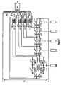
- FIG. 1A A simplified example of a conventional tap changer is shown in Figure 1A .
- the tap changer includes a selector, having two output current paths to select one of a number of taps in the primary winding of the transformer; and a diverter with a "make-before-break" action to divert current from one current path to another without interrupting current flow.
- Figure 1B illustrates the level of complexity that is common within tap changers for power transmission.
- the selector and diverter for a conventional on-load tap changer rely on oil insulation to achieve the contact-to-contact insulation levels required for the highest rated transformer voltage.
- the selector only operates relatively slowly, taking several seconds to change the tap connection, while the diverter must provide a rapid changeover when the selector has made the tap connection in order to limit the level of circulating current. However, this still takes several cycles of power frequency to complete.
- a conventional power network may be described as a network of power stations that provide power to a grid network from which power is then dispersed to consumers through a distribution network.
- tap changers that are smaller, cheaper and easier to install and maintain and that will operate with a wider range of current flow and power factors than existing tap changers.
- tap changers with significantly higher performance to be applied to more novel applications such as phase shifting transformers where the requirement would be to cover the full range of 25 taps within the same time that it presently takes to do one tap change.
- Document DE 41 24431 discloses a protection circuit including at least one resistance connected in series with one of a transformer stepping switch contact and associated with a highpass filter for diverting the transient over voltage.
- An object of the invention is to overcome the problems described above and to meet the foreseen demands of applying distributed generation to localised power distribution.
- Another object of the invention is to provide a tap changer with better properties than those described above, providing a faster change in tap connection without breaking the transformer circuit.
- the invention may be used either to replace the diverter or to replace the complete on-load tap changer system.
- the latter option would require a sufficiently small number of electrical power switches to make it competitive in size and cost to prior art on-load tap changers described above.
- an on-load tap changer according to claim 1.
- the on-load tap changer may further comprise a selector and a diverter, the diverter comprising a pair of opposed switch elements and a commutation circuit, the commutation circuit being operable to establish a resonant current upon closure of a non-conducting switch element to commutate off an arcing switch element.
- the tap changer is intended for association with a transformer for connection to a power system having one or more phases.
- the opposed switch elements may be arranged to provide a "break before make" change over in which opening the switch contacts on current draws an arc between the contacts maintaining conduction past the first break action.
- the concept is that the closure of the second switch will invoke the commutation circuit to quench the arc in the first switch contacts. With a sufficiently fast acting commutation circuit the result is to give an ideal instantaneous change over between the switches.
- an on-load tap changer comprising one or more pairs of opposed switch elements for connection to respective tap windings of a transformer, the tap changer including a commutation circuit being operable to establish a resonant current upon closure of a non-conducting switch element to commutate off an arcing switch element.
- the commutation circuit is included with each opposing switch element to provide an ideal changeover of current in which the closed switch contact opened on load and maintains conduction by drawing an arc between its contacts. Closing the second switch contacts invokes the commutation circuit commutating off the arc across the first switch contacts.
- the operation of the commutation circuit should be very rapid making the changeover of current in the opposing switch element a matter related to the values of voltage and current at the instant of the changeover rather than the conventional consideration of load power factor.
- the changeover scheme provides for a fast reliable switchover, allowing operation at high speed making the resulting tap changer suitable for high performance applications such as in power transmission phase shifting, high voltage D.C. transmission transformers and arc furnace transformers.
- a range of different types of electrical contact could be employed and it is possible to use a semiconductor switch such as a thyristor, for which the term “arcing” should be substituted by "non-gated conduction".
- each switch element is a vacuum switch.
- a vacuum switch will readily arc between the contacts when opened on current, maintaining conduction until the arcing is quenched.
- Vacuum switches require little armature movement to obtain high levels of electrical isolation between contacts so the armature action can be very rapid.
- the small contact gap also means that they arc very readily when being opened on current and several aspects of their design have been introduced to permit arcing to take place without deteriorating their performance such as special contact metals being used that have advantageous properties under arcing. Being plasma in nature, contact arcing is prone to instability under certain conditions.
- Vacuum switches are designed to maintain a high level of arc stability to very low levels of current and voltage (0.5A to 2.5A and 60V being quoted). Unlike arcing that takes place in air, the time to recover the full breakdown voltage for the gap between the contacts is very short. Also, the containment of the arc within the vacuum chamber means that the possibility of contaminating the transformer oil in which it is placed is not possible.
- the tap changer may include a network of opposed switch elements for connection to tap windings with weighted numbers of turns, such that a complete range of integer tap values can be obtained by the tap voltages being caused to subtract or add.
- the network may include a difference winding arrangement, a sum winding arrangement, or a sum-difference winding arrangement.
- the tap windings may have numbers of turns of equal value or weighted as a numerical sequence, which may be binary.
- transformer taps with unequal values can be combined to produce a range of tap values using a minimum of opposing switch elements. Because all the tap winding voltages have the same polarity, passing load current through them in one direction means the tap windings add to the main transformer winding, while passing current in the opposite direction means they subtract from the main transformer winding.
- the simplest scheme is the "difference scheme" in which current passes alternately up and down through the windings as illustrated in Figure 3A .
- the winding values increase as 3N, in a sequence 1, 3, 6, 9.... For example to obtain a tap winding value of 2 the windings are arranged as 3-1, and for 7 the arrangement is 9-3+1.
- FIG. 3B A more complex scheme is the "summation scheme" which is illustrated in Figure 3B and uses true binary windings.
- the switches bypass windings that are not required.
- binary arrangements rise as 2 ⁇ N.
- Figure 3C shows a scheme that combines the sum and difference schemes to reduce the numbers of windings to a minimum. Unfortunately this is at the expense of increased numbers of switches.
- the commutation circuit may include an LC circuit having a capacitor arranged to discharge upon closure of the non-conducting switch element to create the resonant current, the polarity of the resonant current opposing that of the arcing current.
- the resonant current will cancel the transformer load current either before the first resonant peak of the commutation circuit, or at or before the second resonant peak.
- the capacitor may store sufficient charge for the magnitude of the resonant current to sufficiently cancel the transformer load current during at least one cycle such that the combined current through an arcing switch element reduces to less than the chopping current for the switch element.
- the chopping current is set by the properties of the switch used, but will be considered to be approximately zero amperes.
- the commutation circuit must reverse the potential due to the arcing across the contacts of the open switch element on the closure of the opposing switch element in order to quench the arc.
- the reversal of this potential requires that all the current passing through the switch element contacts must be driven to below the chopping current quoted for the switch element. Once the arc is extinguished the time for the switch element to recover is exceptionally short.
- One proposed method utilises the property of capacitors to provide low impedance at high frequency and high impedance at low frequency in contrast with the property of inductors to give high impedance at high frequency and low impedance at low frequency.
- a capacitor placed within a network of inductors and capacitors can be arranged to charge to the tap voltage and to then discharge upon the closure of the non-conducting switch element to create a resonant current.
- the commutation circuit may be balanced.
- balanced is meant that two or more conduction paths of the commutation circuit have identical impedance.
- the advantage of such a scheme is that all the resonant current circulates around the LC network and does not disturb the load current. Also, the extent of the resonance is determined by the polarity of the load current, so a full resonance will not occur when the circulating current due to the capacitor discharge already opposes the direction of the load current.
- this initial circulating current is in the same direction as the load current the capacitor needs to have available sufficient charge to drive the resonance through, for example, a positive peak current and back to a negative peak current, the negative peak current having sufficient magnitude to drive the combined load and resonant current within the arcing contacts through zero, so commutating the arc. This process will result in a reliable commutation process.
- a first load current path has connected in series first and second inductors and a first switch element of an opposed pair.
- a second load current path has connected in series third and fourth inductors and a second switch element of an opposed pair.
- the input connections to the first and third inductors are placed on either side of an isolated transformer tap winding.
- a capacitor bridges a point between the first and second inductors with a point between the third and fourth inductors.
- a first resistor may be connected in shunt with the first inductor, and a second resistor may be connected in shunt with the third inductor, to damp out resonance between these inductors and the resonant capacitance once the arc has been commutated off and the voltage on the capacitor returns to being the tap voltage.
- a voltage-limiting resistor may be connected in shunt with the capacitor.
- the inductance values of the first and third inductors must be equal and similarly the inductance values of the second and fourth inductors (L 2 and L 4 respectively) must also be equal.
- the inductances of the first and second inductors should be related by the equation: L 2 ⁇ 2 3 ⁇ ⁇ ⁇ L 1 , and preferably L 2 ⁇ 0.1 ⁇ L 1 . This ensures that the first and third inductors may present a sufficiently large impedance to the resonant current to substantially decouple the capacitor during commutation.
- a first load current path has a first switch element of an opposed pair.
- a second load current path has connected in series an inductor and a second switch element of the opposed pair.
- a capacitor is connected in shunt with the inductor and the second switch element.
- a first current path has connected in series a first inductor, a second inductor, a first switch element of an opposed pair, and a third inductor.
- First and second resistors are connected in shunt with the first and third inductors respectively.
- a second current path has connected in series a fourth inductor, a fifth inductor, a second switch element of the opposed pair, and a sixth inductor.
- Third and fourth resistors are connected in shunt with the fourth and sixth inductors respectively.
- a first capacitor bridges a point between the first and second inductors and the fourth and fifth inductors.
- a second capacitor bridges a point between the first switch element and the third inductor with a point between the second switch element and sixth inductor.
- a commutation circuit for an on-load tap changer, the commutation circuit being connectable to a pair of opposed switch elements in the tap changer and a tap winding of a transformer, the commutation circuit being operable to establish a resonant current upon closure of a non-conducting switch element to commutate off an arcing switch element.
- the commutation circuit may include any of the features of the tap changers of the first and second aspects of the invention.
- the invention is based on a pair of opposed switch elements 14, 16, as shown in Figure 2 .
- the switch elements 14, 16 When used in an on-load tap changer, the switch elements 14, 16 are arranged to have a momentary "break before make” action.
- a common actuator 18 provides a mechanical drive assembly to produce the required action.
- the switch elements 14, 16 can be driven by individual actuators with electronic timing to provide the required action.
- Such a pair of opposed switch elements can be used to replace the conventional diverter within a conventional on-load tap changer described above.
- one or more pairs of opposed switch elements can be arranged in conjunction with isolated transformer taps to form a complete tap changer, replacing both the selector and the diverter.
- the tap values may be identical.
- the circuit of Figure 3B could be utilised with identical tap winding values.
- the number of taps and opposing switch elements can be significantly reduced.
- Figures 3A, 3B and 3C show simple examples of such tap changers.
- Figure 3A three sets of opposed switch elements are connected so that the intermediate tap values are obtained by subtracting tap voltages, the "difference winding" arrangement.
- Figure 3B four sets of opposed switch elements are connected so that the intermediate tap values are obtained by adding tap voltages, the "sum winding” arrangement.
- Figure 3C shows a further arrangement that combines these two schemes to give intermediate values by both adding and subtracting the tap voltages, the "sum-difference” arrangement.
- the sequence defining the tap winding values vary.
- N i 2 i .
- N i 3 i .
- FIGs 4A to 4D show the four possible permutations of current flow through opposed switch elements 14,16 when connected to a tap winding 12 as in Figures 3A, 3B and 3C .
- the conducting switch has commenced opening on current and is now remaining in conduction as a result of drawing an arc between the contacts. This is represented by the voltage source symbol in the load current path, whose polarity is defined by the direction of flow if the load current, I L .
- This arcing will be sustained until the current passing between the switch contacts reduces to the "chopping current" for the contacts, which for a vacuum switch can be as low as 0.5A. In the context of the normal load current this is negligible, and in the following argument will be treated as zero.
- Closing the opposing switch element causes a circulating current I C to develop, driven by the voltage source representing the transformer tap winding 12 and limited in its rate of rise by inductance within the current loop.
- the circulating current I C adds to the load current I L .
- I C reinforces I L , and it is possible that it can then rise to a level that is large enough to cause damage to the transformer due to the low impedance of the transformer tap winding. This will be referred to as the "reinforcement condition" and is a problem that is overcome by the invention, as will be described.
- FIG. 5 shows part of a tap changer according to a first embodiment of the invention.
- the tap changer includes a commutation circuit and is intended for use with a power transmission transformer to replace the diverter.
- the commutation circuit is connected to first and second opposed switch elements operated by an actuator, and to a tap winding, represented in Figure 5 by a voltage source.
- the commutation circuit has two load current paths.
- a first load current path has connected in series first and second inductors and a first switch element of an opposed pair.
- a second load current path has connected in series third and fourth inductors and a second switch element of the opposed pair.
- a capacitor bridges a point between the first and second inductors with a point between the third and fourth inductors.
- the capacitor charges to near the instantaneous voltage of the voltage source representing the tap winding.
- Values of inductance and capacitance are chosen such that, on closing the non conducting switch element, the magnitude of the second peak of the resonant current exceeds that of the load current, causing the current in the arcing switch element to pass through zero, thereby commutating off the arcing switch element.
- the natural frequency for the commutation circuit is a matter of design choice and will normally be greater than 1kHz and may be as high as 100kHz. A higher frequency requires smaller components, but too high a frequency result in damping effects due to eddy currents in the circuit and particularly within the switch element.
- the capacitor needs to have a very high rated voltage and must have a relatively low value of self-resonance that should not be permitted to conflict with the selected resonant frequency.
- the inductance values of the first and third inductors are chosen to present sufficiently large impedance to the resonant current for the capacitor to substantially decouple the voltage source. Significantly, this ensures that the resonant current is contained within the commutation circuit, with the load current remaining unaffected.
- the inductance values of the first to fourth inductors are L 1 , L 2 , L 3 and L 4 .
- L 1 and L 2 (and hence L 3 and L 4 ) must be related by the equation: L 2 ⁇ 2 3 ⁇ ⁇ ⁇ L 1 . This ensures that the magnitude of the resonant current will be sufficient to be able to cancel the load current.
- the damping resistor is then selected to give minimum damping of the initial commutation resonance while providing a minimum number of resonant cycles after commutation.
- the non-linear resistance placed across the capacitance must limit the capacitor voltage to a value less than the capacitor rated voltage but more that the worst case maximum peak voltage to be expected. Hence all the component values in the circuit can be found. In practice some adjustment may be required to account for effects such as damping due to eddy currents within the vacuum switch or stray circuit inductance.
- the maximum peak resonant current will be very high for the commutation at maximum peak voltage. None of the inductors must saturate and the capacitor must be rated for this current. Similarly after commutation has occurred the current built up within the "blocking" inductor L 1 , must now pass directly through the resonant capacitor, causing this to reverse in potential and to reach a voltage several times the normal supply voltage if it is not suppressed.
- the following give derived expressions to provide an approximate indication of the magnitudes of the various voltages and currents that affect the component design.
- V cc 0.1 1.1 ⁇ V 0
- V cc 0.1 1.1 ⁇ V 0
- the size of the components can be significant compared to the size of the switch assembly. Since the commutation process employs current that wholly circulates through the capacitor the two pairs of inductors L 1 /L 3 and L 2 /L 4 may be combined as mutually coupled inductors on a common magnetic core. This exploits the phenomena that inductance is proportional to the number of turns squared. Thus two identical coils which have a common current passing through them in the same direction will develop a total inductance of four times that of the individual inductors. However, if the current flows in opposing directions through the coils, the flux cancels resulting in no net inductance being present. Thus the pair of coils can be placed on a single core of the same size as for each of the previous coils, where the number of turns for each coil winding is reduced in value by the square root of two.
- the circuit presented in Figure 5 may be directly applied as a replacement to a diverter in a conventional on-load tap changer.
- connection of the capacitance in parallel with the tap windings might present a problem with selectors that switch in oil.
- it may be necessary to introduce two additional auxiliary contacts as in Figure 6 so that this capacitance can be isolated while the selector is being operated.
- the commutation circuit can be applied directly or may need to be modified to allow it to be incorporated into different forms of tap changers such as those shown in Figures 3A, 3B and 3C .
- L 2 and L 4 means that stray terms within the current path may provide sufficient inductance without the need for those inductors.
- Figure 7 shows a complete tap changer having a difference winding arrangement and incorporating a modified form of the commutation circuit of the first embodiment.
- the inductors L 1 , L 3 and the resonant capacitor are associated with the tap winding, while the inductors L 2 and L 4 are associated with the opposed switch pair.
- L 1 and L 3 have been designed as mutually coupled inductors but cannot be applied to this configuration to L 2 and L 4 .
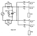
- opposing switch element S5 uses pairs of switches in series with voltage sharing Metal Oxide Varistors (MOVs) in order to obtain the required breakdown insulation voltage (BIL) for the highest tap voltage.
- MOVs Metal Oxide Varistors
- Figure 8A shows a complete tap changer having a sum winding arrangement and directly incorporating the commutation circuit of the first embodiment.
- L 2 and L 4 have been implemented as mutually coupled inductors to reduce their size and cost.
- opposing switch pair S5 needs to form a full bridge circuit to provide a voltage reversal. Since the BIL is above that for the individual switches, series connected pairs of switches have had to be used as with Figure 7 .
- Figure 8B shows how separating out part of the primary winding to give an additional 16.Nt tap winding may reduce the complexity of this circuit.
- Any of the commutation circuits herein may be used in such a way as to form a complete tap changer.
- any embodiment shown and described may be used to replace a conventional diverter simply by omitting the tap winding and instead connecting the two resulting free points to the selector such that the two load current paths of the circuit connect respectively to the two current paths of the selector.
- Figure 9 shows part of a tap changer according to a second embodiment of the invention.
- the tap changer includes a commutation circuit 400.
- the commutation circuit 400 has two load current paths.
- a first load current path has a first switch contact 414 of an opposed switch pair.
- a second load current path has connected in series an inductor 401 and a second electrical contact 416 of the opposed switch pair.
- a capacitor 411 is connected in shunt with the inductor 401 and second switch contact 416.
- FIG. 10 shows part of a tap changer according to a third embodiment of the invention.
- the tap changer includes a commutation circuit 500 and is intended for use with a distribution transformer.
- the commutation circuit essentially mirrors that of the first embodiment. The principle is the same except that the resonant current passes through the second 502 and fifth 505 inductors and both capacitors 510, 511.
- the commutation circuit 500 has two load current paths.
- a first current path has connected in series a first inductor 501, a second inductor 502, a first electrical switch contact 514 of an opposed switch pair, and a third inductor 503.
- First 521 and second 522 resistors are connected in shunt with the first 501 and third 503 inductors respectively.
- a second current path has connected in series a fourth inductor 504, a fifth inductor 505, a second electrical switch contact 516 of the opposed switch pair, and a sixth inductor 506.
- Third 523 and fourth 524 resistors are connected in shunt with the fourth 504 and sixth 506 inductors respectively.
- a first capacitor 510 bridges a point between the first 501 and second 502 inductors with a point between the fourth 504 and fifth 505 inductors.
- a second capacitor 511 bridges a point between the first electrical switch contact 514 and third inductor 503 with a point between the second electrical switch contact 516 and sixth inductor 506.
- the quenching of the arc means that the capacitor voltage is now significantly different from its steady state value of equalling the tap voltage.
- the current in the two outer inductors (i.e. 501 and 503 or 504 and 506) in load current path that has now been disconnected still have current present in them that must be dissipated.
- the presence of the inductor currents actually causes the resonant capacitor to swing further away from its steady state voltage leading to a large resonance that must be suppressed to prevent re-strike on the open electrical switch contacts.
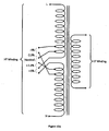
- Figure 12A shows a tap arrangement of a distribution transformer, with which the tap changer of Figure 11A may be used.
- the required tap setting is obtained by shorting between any two of the adjacent tap connections.
- a rack and pinion assembly is used, the shorting link being attached to the rack and a winding handle being attached to the pinion.
- This form of tap change can only be used with the tap changer off-load and isolated.
- Figure 12B illustrates how the on-load tap changer given in Figure 11A might be coupled into the distribution transformer to provide the ability to switch between two pre-selected tap settings.
- the first embodiment of the invention provides the most straightforward implementation of the invention, providing symmetry and balance. This can be used directly as either a diverter or as part of a tap changer. When used as a diverter, the presence of the capacitor directly across the transformer winding may present problems for the switchgear providing the selector function. The relatively high value of this means that arcing may well take place on closing and opening contacts and so using "switching-in-oil" techniques may cause degradation of the selector contacts and the insulation properties of the oil in which it is placed. In this event, auxiliary contacts will need to be included within the diverter, for example as indicated in Figure 6 . The auxiliary contact in the non-conducting path would be opened prior to any operation to change state taking place within the selector. The auxiliary contacts would use vacuum switches to contain any arcing that might take place.
- the second and third embodiments of the invention are not symmetrical or balanced although they might be developed to this. Thus they will only function for a restricted load power factor and their operation disrupts the load current during the commutation operation.
- the fourth embodiment has been shown in operation within a distribution transformer. However, it may also be applied to derivatives of the difference tap changer form, although this can lead to an increase in the component count.
- the component count is reduced.
- Arcing relies on ionised particles being drawn across the contact gap, so once the arc has been extinguished there must be sufficient time for the particles remaining in the gap to condense.
- vacuum switches means this time is very short and there is a risk that if this process occurs too rapidly the arc might re-strike with the risk that the circulating current might commence developing in the opposite polarity. This is particularly so if the "chopping current" level is high and the inductance in series with the switch contacts is relatively high.
- Figure 13 shows a simulation of the electrical circuit shown in Figure 5 using the SimPower Systems Blockset within MATLAB to represent a 70MVA transformer with a 227kV primary supply voltage and a 1% tap winding.
- the transformer is fully loaded with a 0.8 power factor.
- the commutation components have been calculated on the basis of a commutation frequency of 50kHz.
- the Mayr Arc model has been used for the arcing switch as provided by Delft University (ref. 3). This model uses a controlled current source for output which requires defined initial impedance, so all the inductors associated with this element require parallel connected resistors. These have all been given a nominal 1k ⁇ value and are not listed below.
- Table 1 Component Description Component Reference Component Value Primary Inductance 0.84H Primary Resistance 1.946 ⁇ Tap Inductance 0.376mH Tap Resistance 42m ⁇ Load Resistance 736 ⁇ Load Inductance 1.4H Magnetising Inductance 4059H Magnetising Resistance 1.571M ⁇ Primary Voltage 227kV r.m.s. Tap Winding Voltage 3.017kV r.m.s L1 & L3 50 ⁇ H L2 & L4 5 ⁇ H C 2.2 ⁇ F L1 & L3 Damping Resistors 1 ⁇ Surge arrestor voltage 4kV
- Table 1 shows the calculated design parameters around which the component design would be based.
- Table 2 Parameter Description Value Steady state capacitor current 1.2A rms Steady state inductor impedance 16m ⁇ Peak L2/L4 commutation current 1.19kA Peak L1/L3 commutation current 704A ⁇ Capacitor voltage at commutation 112V Capacitor deviation from steady state -1.12kV Unsuppressed peak capacitor voltage after commutation (in addition to voltage at instant of commutation) 3.5kV
- the model shows five cycles of operation with the opening contact commencing to arc at 35ms into the simulation.
- the closing contact is then closed 36ms into the simulation.
- Figure 14 shows the load current and voltage indicating that no disturbance is created during the tap change process.
- Figure 15 shows the currents in the opposing pair contacts, and the capacitor voltage, with no apparent deviation in the 50Hz nature of the waveform until the instant of contact closure, when the commutation resonance occurs.
- the capacitor voltage would swing to a negative voltage in excess of 8kV without the presence of the surge arrestor. This is due to the surplus energy built up in the inductors L1 & L3 during the commutation process. Additional over-voltage suppression will clearly be necessary.
Landscapes
- Engineering & Computer Science (AREA)
- Power Engineering (AREA)
- High-Tension Arc-Extinguishing Switches Without Spraying Means (AREA)
- Axle Suspensions And Sidecars For Cycles (AREA)
- Amplifiers (AREA)
- Solid-Sorbent Or Filter-Aiding Compositions (AREA)
Abstract
Description
- The invention relates to on-load tap changers, and in particular to commutation in on-load tap changers.
- A tap changer is a device fitted to a transformer for regulating the output voltage of the transformer to a required level. Such regulation is normally achieved by selectively connecting to particular taps of the transformer, thereby controlling the number of turns in the active portion of the primary or secondary winding (ref. 1).
- An on-load tap changer is designed to operate when conducting current and requires that the circuit must not be opened even momentarily during tap changing.
- A simplified example of a conventional tap changer is shown in
Figure 1A . The tap changer includes a selector, having two output current paths to select one of a number of taps in the primary winding of the transformer; and a diverter with a "make-before-break" action to divert current from one current path to another without interrupting current flow.Figure 1B illustrates the level of complexity that is common within tap changers for power transmission. - Conventional tap changers achieve the "make-before-break" action by connecting resistors across the tap winding during the moment of changeover to limit circulating current that would otherwise develop. The breaking of this combined load current and circulating current using conventional high voltage electrical switch contacts leads to a high level of arcing occurring. This both degrades the insulating property of the oil in which the switch is placed and occasionally leads to the mechanism "sticking". The former of these conditions requires that the oil is segregated from the main transformer oil and that it must be replaced on a regular basis, while the latter can lead to catastrophic failure of the whole transformer system. Modern systems include a vacuum switch to contain the arc but this adds complexity and the vacuum switch requires regular replacement (ref. 2).
- The selector and diverter for a conventional on-load tap changer rely on oil insulation to achieve the contact-to-contact insulation levels required for the highest rated transformer voltage. The selector only operates relatively slowly, taking several seconds to change the tap connection, while the diverter must provide a rapid changeover when the selector has made the tap connection in order to limit the level of circulating current. However, this still takes several cycles of power frequency to complete.
- A conventional power network may be described as a network of power stations that provide power to a grid network from which power is then dispersed to consumers through a distribution network. There is a trend towards more localised generation, supported by national and international legislation, which will require much more flexibility in the manner in which the power is managed at a local level. This will require tap changers that are smaller, cheaper and easier to install and maintain and that will operate with a wider range of current flow and power factors than existing tap changers. Moreover there is a requirement for tap changers with significantly higher performance to be applied to more novel applications such as phase shifting transformers where the requirement would be to cover the full range of 25 taps within the same time that it presently takes to do one tap change.
- Document
DE 41 24431 discloses a protection circuit including at least one resistance connected in series with one of a transformer stepping switch contact and associated with a highpass filter for diverting the transient over voltage. - An object of the invention is to overcome the problems described above and to meet the foreseen demands of applying distributed generation to localised power distribution.
- Another object of the invention is to provide a tap changer with better properties than those described above, providing a faster change in tap connection without breaking the transformer circuit.
- The invention may be used either to replace the diverter or to replace the complete on-load tap changer system. The latter option would require a sufficiently small number of electrical power switches to make it competitive in size and cost to prior art on-load tap changers described above.
- According to the invention, there is provided an on-load tap changer according to
claim 1. - The on-load tap changer may further comprise a selector and a diverter, the diverter comprising a pair of opposed switch elements and a commutation circuit, the commutation circuit being operable to establish a resonant current upon closure of a non-conducting switch element to commutate off an arcing switch element.
- The tap changer is intended for association with a transformer for connection to a power system having one or more phases.
- The opposed switch elements may be arranged to provide a "break before make" change over in which opening the switch contacts on current draws an arc between the contacts maintaining conduction past the first break action. The concept is that the closure of the second switch will invoke the commutation circuit to quench the arc in the first switch contacts. With a sufficiently fast acting commutation circuit the result is to give an ideal instantaneous change over between the switches.
- According to the invention, there is provided an on-load tap changer comprising one or more pairs of opposed switch elements for connection to respective tap windings of a transformer, the tap changer including a commutation circuit being operable to establish a resonant current upon closure of a non-conducting switch element to commutate off an arcing switch element.
- The commutation circuit is included with each opposing switch element to provide an ideal changeover of current in which the closed switch contact opened on load and maintains conduction by drawing an arc between its contacts. Closing the second switch contacts invokes the commutation circuit commutating off the arc across the first switch contacts. By using an array of electrically isolated transformer taps as part of a network of such opposing switch elements, a complete tap changer can be assembled, with no requirement to distinguish between a selector and diverter. Furthermore, by employing isolated tap windings with turns values that vary one to another according to a set sequence, for example binary, the required number of windings and switch elements can be significantly reduced over that of a conventional tap changer.
- The operation of the commutation circuit should be very rapid making the changeover of current in the opposing switch element a matter related to the values of voltage and current at the instant of the changeover rather than the conventional consideration of load power factor. Thus the changeover scheme provides for a fast reliable switchover, allowing operation at high speed making the resulting tap changer suitable for high performance applications such as in power transmission phase shifting, high voltage D.C. transmission transformers and arc furnace transformers.
- A range of different types of electrical contact could be employed and it is possible to use a semiconductor switch such as a thyristor, for which the term "arcing" should be substituted by "non-gated conduction".
- However, in a preferred embodiment, each switch element is a vacuum switch. A vacuum switch will readily arc between the contacts when opened on current, maintaining conduction until the arcing is quenched. Vacuum switches require little armature movement to obtain high levels of electrical isolation between contacts so the armature action can be very rapid. The small contact gap also means that they arc very readily when being opened on current and several aspects of their design have been introduced to permit arcing to take place without deteriorating their performance such as special contact metals being used that have advantageous properties under arcing. Being plasma in nature, contact arcing is prone to instability under certain conditions. Vacuum switches are designed to maintain a high level of arc stability to very low levels of current and voltage (0.5A to 2.5A and 60V being quoted). Unlike arcing that takes place in air, the time to recover the full breakdown voltage for the gap between the contacts is very short. Also, the containment of the arc within the vacuum chamber means that the possibility of contaminating the transformer oil in which it is placed is not possible.
- The tap changer may include a network of opposed switch elements for connection to tap windings with weighted numbers of turns, such that a complete range of integer tap values can be obtained by the tap voltages being caused to subtract or add. The network may include a difference winding arrangement, a sum winding arrangement, or a sum-difference winding arrangement. The tap windings may have numbers of turns of equal value or weighted as a numerical sequence, which may be binary.
- There are several different ways in which transformer taps with unequal values can be combined to produce a range of tap values using a minimum of opposing switch elements. Because all the tap winding voltages have the same polarity, passing load current through them in one direction means the tap windings add to the main transformer winding, while passing current in the opposite direction means they subtract from the main transformer winding. The simplest scheme is the "difference scheme" in which current passes alternately up and down through the windings as illustrated in
Figure 3A . The winding values increase as 3N, in asequence Figure 3B and uses true binary windings. Here the switches bypass windings that are not required. To illustrate the degree of reduction possible in the numbers of switches it is well known that binary arrangements rise as 2^N. Thus with 5 opposing switch elements it should be possible to obtain 32 different tap combinations. With the circuit shown inFigure 3B a reversing function has been added that requires an extra opposing switch pair, so to cover a typical range of -12 to +12 would require six sets of opposing switch combinations and five tap windings.Figure 3C shows a scheme that combines the sum and difference schemes to reduce the numbers of windings to a minimum. Unfortunately this is at the expense of increased numbers of switches. - The commutation circuit may include an LC circuit having a capacitor arranged to discharge upon closure of the non-conducting switch element to create the resonant current, the polarity of the resonant current opposing that of the arcing current.
- Depending on the polarity of the transformer load current, the resonant current will cancel the transformer load current either before the first resonant peak of the commutation circuit, or at or before the second resonant peak.
- The capacitor may store sufficient charge for the magnitude of the resonant current to sufficiently cancel the transformer load current during at least one cycle such that the combined current through an arcing switch element reduces to less than the chopping current for the switch element. The chopping current is set by the properties of the switch used, but will be considered to be approximately zero amperes.
- The commutation circuit must reverse the potential due to the arcing across the contacts of the open switch element on the closure of the opposing switch element in order to quench the arc. The reversal of this potential requires that all the current passing through the switch element contacts must be driven to below the chopping current quoted for the switch element. Once the arc is extinguished the time for the switch element to recover is exceptionally short.
- One proposed method utilises the property of capacitors to provide low impedance at high frequency and high impedance at low frequency in contrast with the property of inductors to give high impedance at high frequency and low impedance at low frequency. Thus with the conducting switch element contacts open and arcing to maintain conduction the action of closing the opposing switch element contacts applies a step voltage through a pair of capacitors which momentarily reverses the voltage on the arcing contacts. This is allowed to occur due to the presence of two inductors. The time constant of this action is very short so these components would not interfere with the normal operation of the tap changer.
- A capacitor placed within a network of inductors and capacitors (LC network) can be arranged to charge to the tap voltage and to then discharge upon the closure of the non-conducting switch element to create a resonant current.
- The commutation circuit may be balanced. By "balanced" is meant that two or more conduction paths of the commutation circuit have identical impedance.
- The advantage of such a scheme is that all the resonant current circulates around the LC network and does not disturb the load current. Also, the extent of the resonance is determined by the polarity of the load current, so a full resonance will not occur when the circulating current due to the capacitor discharge already opposes the direction of the load current. When this initial circulating current is in the same direction as the load current the capacitor needs to have available sufficient charge to drive the resonance through, for example, a positive peak current and back to a negative peak current, the negative peak current having sufficient magnitude to drive the combined load and resonant current within the arcing contacts through zero, so commutating the arc. This process will result in a reliable commutation process.
- In a first embodiment, a first load current path has connected in series first and second inductors and a first switch element of an opposed pair. A second load current path has connected in series third and fourth inductors and a second switch element of an opposed pair. The input connections to the first and third inductors are placed on either side of an isolated transformer tap winding. A capacitor bridges a point between the first and second inductors with a point between the third and fourth inductors.
- A first resistor may be connected in shunt with the first inductor, and a second resistor may be connected in shunt with the third inductor, to damp out resonance between these inductors and the resonant capacitance once the arc has been commutated off and the voltage on the capacitor returns to being the tap voltage. A voltage-limiting resistor may be connected in shunt with the capacitor.
- To provide a balanced circuit the inductance values of the first and third inductors (L1 and L3 respectively) must be equal and similarly the inductance values of the second and fourth inductors (L2 and L4 respectively) must also be equal.
- The inductances of the first and second inductors (and hence the third and fourth inductors) should be related by the equation:

- Finally

- In a second embodiment, a first load current path has a first switch element of an opposed pair. A second load current path has connected in series an inductor and a second switch element of the opposed pair. A capacitor is connected in shunt with the inductor and the second switch element.
- In a third embodiment, a first current path has connected in series a first inductor, a second inductor, a first switch element of an opposed pair, and a third inductor. First and second resistors are connected in shunt with the first and third inductors respectively. A second current path has connected in series a fourth inductor, a fifth inductor, a second switch element of the opposed pair, and a sixth inductor. Third and fourth resistors are connected in shunt with the fourth and sixth inductors respectively. A first capacitor bridges a point between the first and second inductors and the fourth and fifth inductors. A second capacitor bridges a point between the first switch element and the third inductor with a point between the second switch element and sixth inductor.
- According to a third aspect of the invention, there is provided a commutation circuit for an on-load tap changer, the commutation circuit being connectable to a pair of opposed switch elements in the tap changer and a tap winding of a transformer, the commutation circuit being operable to establish a resonant current upon closure of a non-conducting switch element to commutate off an arcing switch element.
- The commutation circuit may include any of the features of the tap changers of the first and second aspects of the invention.
- In order that the invention may be more readily understood, a description is now given, by way of example only, reference being made to the accompanying drawings, in which:-
-
Figure 1A is a schematic diagram of a simplified example of a conventional on-load tap changer; -
Figure 1B is a schematic diagram illustrating a more typical selector arrangement for a power transmission transformer to obtain a tap range of ±12 (ref. 1) ; -
Figure 2 is a schematic diagram of a pair of opposed switch elements operated using a common actuator; -
Figures 3A to 3C are schematic diagrams of opposed pairs of switch elements in a difference winding arrangement; a sum winding arrangement; and a sum-difference winding arrangement, respectively; -
Figures 4A to 4D are schematic diagrams showing circulating current flow and various permutations of load current through opposed pairs of switch elements; -
Figure 5 is a schematic diagram of a commutation circuit according to a first embodiment of the invention; -
Figure 6 is a schematic diagram of a modification to the circuit ofFigure 5 so that it can act in place of a conventional diverter; -
Figure 7 is a schematic diagram of a complete tap changer having a difference winding arrangement giving ±12 taps and incorporating the circuit ofFigure 6 ; -
Figure 8A is a schematic diagram of a complete tap changer having a sum winding arrangement giving ±15 taps and incorporating the circuit ofFigure 6 ; -
Figure 8B is a schematic diagram of a complete tap changer having a sum winding arrangement giving +31 taps and incorporating the circuit ofFigure 6 (note Np*=Np-16.Nt); -
Figure 9 is a schematic diagram of a commutation circuit according to a second embodiment of the invention; -
Figure 10 is a schematic diagram of a commutation circuit according to a third embodiment of the invention; -
Figure 11A is a schematic diagram of a commutation circuit according to a fourth embodiment of the invention; -
Figure 11B is a schematic diagram of the circuit ofFigure 11A applied to a derivative of the difference tap changer form, rather than a distribution transformer; -
Figure 12A is a schematic diagram of a split tapped primary winding with which the circuit ofFigure 11 is used; -
Figure 12B illustrates how the circuit ofFigure 11 might be connected to the winding ofFigure 12A ; -
Figure 13 is a MATLAB/SimPower Systems representation of a 70MVA power transmission transformer with a 227kV r.m.s. nominal primary rating used to simulate the operation of a tap changer according to the invention; -
Figure 14 illustrates the results for the load current and voltage waveforms of the simulation ofFigure 13 when undergoing a tap change; -
Figure 15 illustrates the results for the currents in the opposed pair of switch elements (top trace) and the commutation capacitor voltage (bottom trace); -
Figure 16 shows an expansion ofFigure 15 to show the commutation process. - The invention is based on a pair of
opposed switch elements Figure 2 . - When used in an on-load tap changer, the
switch elements common actuator 18 provides a mechanical drive assembly to produce the required action. Alternatively, theswitch elements - Such a pair of opposed switch elements can be used to replace the conventional diverter within a conventional on-load tap changer described above.
- Alternatively, one or more pairs of opposed switch elements can be arranged in conjunction with isolated transformer taps to form a complete tap changer, replacing both the selector and the diverter.
- The tap values may be identical. For example, the circuit of
Figure 3B could be utilised with identical tap winding values. However, by using tap windings with individual winding values, the number of taps and opposing switch elements can be significantly reduced. -
Figures 3A, 3B and3C show simple examples of such tap changers. InFigure 3A , three sets of opposed switch elements are connected so that the intermediate tap values are obtained by subtracting tap voltages, the "difference winding" arrangement. InFigure 3B , four sets of opposed switch elements are connected so that the intermediate tap values are obtained by adding tap voltages, the "sum winding" arrangement.Figure 3C shows a further arrangement that combines these two schemes to give intermediate values by both adding and subtracting the tap voltages, the "sum-difference" arrangement. In the proposed arrangements, the sequence defining the tap winding values vary. For the difference scheme, the number of turns (Ni) for the ith tap winding is given as: Ni =3·i. For the sum scheme, the number of turns (Ni) for the ith tap winding is given as: Ni =2 i . For the sum-difference scheme, the number of turns (Ni) for the ith tap winding is given as: Ni =3 i . -
Figures 4A to 4D show the four possible permutations of current flow through opposedswitch elements Figures 3A, 3B and3C . In all these diagrams, it has been assumed that the conducting switch has commenced opening on current and is now remaining in conduction as a result of drawing an arc between the contacts. This is represented by the voltage source symbol in the load current path, whose polarity is defined by the direction of flow if the load current, IL. This arcing will be sustained until the current passing between the switch contacts reduces to the "chopping current" for the contacts, which for a vacuum switch can be as low as 0.5A. In the context of the normal load current this is negligible, and in the following argument will be treated as zero. Closing the opposing switch element causes a circulating current IC to develop, driven by the voltage source representing the transformer tap winding 12 and limited in its rate of rise by inductance within the current loop. - In
Figures 4A and 4C the circulating current IC opposes the load current IL. Thus IC will continually rise until it reaches the value of IL and cancels it, quenching the arc. This will be referred to as the "cancellation condition". - In
Figures 4B and 4D , the circulating current IC adds to the load current IL. IC reinforces IL, and it is possible that it can then rise to a level that is large enough to cause damage to the transformer due to the low impedance of the transformer tap winding. This will be referred to as the "reinforcement condition" and is a problem that is overcome by the invention, as will be described. -
Figure 5 shows part of a tap changer according to a first embodiment of the invention. The tap changer includes a commutation circuit and is intended for use with a power transmission transformer to replace the diverter. - The commutation circuit is connected to first and second opposed switch elements operated by an actuator, and to a tap winding, represented in
Figure 5 by a voltage source. - The commutation circuit has two load current paths. A first load current path has connected in series first and second inductors and a first switch element of an opposed pair. A second load current path has connected in series third and fourth inductors and a second switch element of the opposed pair. A capacitor bridges a point between the first and second inductors with a point between the third and fourth inductors.
- In use, the capacitor charges to near the instantaneous voltage of the voltage source representing the tap winding.
- In the cancellation condition, closing the non-conducting switch element results in the arc being quenched naturally, as described above.
- In the reinforcement condition, closing the non-conducting switch element creates a discharge path for the capacitor, while the second and fourth inductors create a sinusoidal resonant current. This current will initially rise in the same sense as the load current. However, it will then swing back to oppose the load current in the arcing switch element with sufficient magnitude to quench the arc.
- In this way, the arc is quenched for all permutations of load current flow.
- Values of inductance and capacitance are chosen such that, on closing the non conducting switch element, the magnitude of the second peak of the resonant current exceeds that of the load current, causing the current in the arcing switch element to pass through zero, thereby commutating off the arcing switch element.
- The natural frequency for the commutation circuit is a matter of design choice and will normally be greater than 1kHz and may be as high as 100kHz. A higher frequency requires smaller components, but too high a frequency result in damping effects due to eddy currents in the circuit and particularly within the switch element. In particular the capacitor needs to have a very high rated voltage and must have a relatively low value of self-resonance that should not be permitted to conflict with the selected resonant frequency.
- The inductance values of the first and third inductors are chosen to present sufficiently large impedance to the resonant current for the capacitor to substantially decouple the voltage source. Significantly, this ensures that the resonant current is contained within the commutation circuit, with the load current remaining unaffected.
- The inductance values of the first to fourth inductors are L1, L2, L3 and L4. In this embodiment, L1 = L3 and L2= L4, i.e. the commutation circuit is balanced having equal impedance in both current paths. This mitigates 'ringing' on the load current after a switchover with any ringing being contained within the loop.
- The inductor values L1 and L2 (and hence L3 and L4) must be related by the equation:

- For the
relationship 
- The design value of L2 is found by selecting the desired resonant frequency ω radians per second) and substituting it into the
expression 

- The damping resistor is then selected to give minimum damping of the initial commutation resonance while providing a minimum number of resonant cycles after commutation. The non-linear resistance placed across the capacitance must limit the capacitor voltage to a value less than the capacitor rated voltage but more that the worst case maximum peak voltage to be expected. Hence all the component values in the circuit can be found. In practice some adjustment may be required to account for effects such as damping due to eddy currents within the vacuum switch or stray circuit inductance.
- The maximum peak resonant current will be very high for the commutation at maximum peak voltage. None of the inductors must saturate and the capacitor must be rated for this current. Similarly after commutation has occurred the current built up within the "blocking" inductor L1, must now pass directly through the resonant capacitor, causing this to reverse in potential and to reach a voltage several times the normal supply voltage if it is not suppressed. The following give derived expressions to provide an approximate indication of the magnitudes of the various voltages and currents that affect the component design.
- The current in L1 at commutation is given as:

- And the current in L2 at commutation is given as:

- The voltage at commutation is


The peak capacitor voltage after commutation has taken place is given as:
- The size of the components can be significant compared to the size of the switch assembly. Since the commutation process employs current that wholly circulates through the capacitor the two pairs of inductors L1/L3 and L2/L4 may be combined as mutually coupled inductors on a common magnetic core. This exploits the phenomena that inductance is proportional to the number of turns squared. Thus two identical coils which have a common current passing through them in the same direction will develop a total inductance of four times that of the individual inductors. However, if the current flows in opposing directions through the coils, the flux cancels resulting in no net inductance being present. Thus the pair of coils can be placed on a single core of the same size as for each of the previous coils, where the number of turns for each coil winding is reduced in value by the square root of two.
- The circuit presented in
Figure 5 may be directly applied as a replacement to a diverter in a conventional on-load tap changer. In doing this it, should be noted that the connection of the capacitance in parallel with the tap windings might present a problem with selectors that switch in oil. In this case, it may be necessary to introduce two additional auxiliary contacts as inFigure 6 , so that this capacitance can be isolated while the selector is being operated. - The commutation circuit can be applied directly or may need to be modified to allow it to be incorporated into different forms of tap changers such as those shown in
Figures 3A, 3B and3C . - The low values of L2 and L4 means that stray terms within the current path may provide sufficient inductance without the need for those inductors.
-
Figure 7 shows a complete tap changer having a difference winding arrangement and incorporating a modified form of the commutation circuit of the first embodiment. Note that the inductors L1, L3 and the resonant capacitor are associated with the tap winding, while the inductors L2 and L4 are associated with the opposed switch pair. In this L1 and L3 have been designed as mutually coupled inductors but cannot be applied to this configuration to L2 and L4. Note that opposing switch element S5 uses pairs of switches in series with voltage sharing Metal Oxide Varistors (MOVs) in order to obtain the required breakdown insulation voltage (BIL) for the highest tap voltage. -
Figure 8A shows a complete tap changer having a sum winding arrangement and directly incorporating the commutation circuit of the first embodiment. In this example, L2 and L4 have been implemented as mutually coupled inductors to reduce their size and cost. In this example, opposing switch pair S5 needs to form a full bridge circuit to provide a voltage reversal. Since the BIL is above that for the individual switches, series connected pairs of switches have had to be used as withFigure 7 .Figure 8B shows how separating out part of the primary winding to give an additional 16.Nt tap winding may reduce the complexity of this circuit. - Any of the commutation circuits herein may be used in such a way as to form a complete tap changer.
- Alternatively, any embodiment shown and described may be used to replace a conventional diverter simply by omitting the tap winding and instead connecting the two resulting free points to the selector such that the two load current paths of the circuit connect respectively to the two current paths of the selector.
-
Figure 9 shows part of a tap changer according to a second embodiment of the invention. The tap changer includes acommutation circuit 400. - The
commutation circuit 400 has two load current paths. A first load current path has afirst switch contact 414 of an opposed switch pair. A second load current path has connected in series aninductor 401 and a secondelectrical contact 416 of the opposed switch pair. Acapacitor 411 is connected in shunt with theinductor 401 andsecond switch contact 416. -
Figure 10 shows part of a tap changer according to a third embodiment of the invention. The tap changer includes acommutation circuit 500 and is intended for use with a distribution transformer. - The commutation circuit essentially mirrors that of the first embodiment. The principle is the same except that the resonant current passes through the second 502 and fifth 505 inductors and both capacitors 510, 511.
- The
commutation circuit 500 has two load current paths. A first current path has connected in series afirst inductor 501, asecond inductor 502, a firstelectrical switch contact 514 of an opposed switch pair, and athird inductor 503. First 521 and second 522 resistors are connected in shunt with the first 501 and third 503 inductors respectively. A second current path has connected in series afourth inductor 504, afifth inductor 505, a secondelectrical switch contact 516 of the opposed switch pair, and asixth inductor 506. Third 523 and fourth 524 resistors are connected in shunt with the fourth 504 and sixth 506 inductors respectively. A first capacitor 510 bridges a point between the first 501 and second 502 inductors with a point between the fourth 504 and fifth 505 inductors. A second capacitor 511 bridges a point between the firstelectrical switch contact 514 andthird inductor 503 with a point between the secondelectrical switch contact 516 andsixth inductor 506. - The four resistors 521-524 connected in shunt respectively with the first, second, fifth and
sixth inductors -
Figure 12A shows a tap arrangement of a distribution transformer, with which the tap changer ofFigure 11A may be used. The required tap setting is obtained by shorting between any two of the adjacent tap connections. In practice, a rack and pinion assembly is used, the shorting link being attached to the rack and a winding handle being attached to the pinion. This form of tap change can only be used with the tap changer off-load and isolated.Figure 12B illustrates how the on-load tap changer given inFigure 11A might be coupled into the distribution transformer to provide the ability to switch between two pre-selected tap settings. - The first embodiment of the invention provides the most straightforward implementation of the invention, providing symmetry and balance. This can be used directly as either a diverter or as part of a tap changer. When used as a diverter, the presence of the capacitor directly across the transformer winding may present problems for the switchgear providing the selector function. The relatively high value of this means that arcing may well take place on closing and opening contacts and so using "switching-in-oil" techniques may cause degradation of the selector contacts and the insulation properties of the oil in which it is placed. In this event, auxiliary contacts will need to be included within the diverter, for example as indicated in
Figure 6 . The auxiliary contact in the non-conducting path would be opened prior to any operation to change state taking place within the selector. The auxiliary contacts would use vacuum switches to contain any arcing that might take place. - The second and third embodiments of the invention are not symmetrical or balanced although they might be developed to this. Thus they will only function for a restricted load power factor and their operation disrupts the load current during the commutation operation.
- The fourth embodiment has been shown in operation within a distribution transformer. However, it may also be applied to derivatives of the difference tap changer form, although this can lead to an increase in the component count. By associating the resonant capacitors and the blocking inductors with specific windings as in
Figure 11B and applied inFigure 7 , the component count is reduced. - There is a possibility that stray EMC coupling, including capacitance between the tap winding and the core, may disturb the predicted operation of the scheme. If this is neglected, for the summation scheme, the predicted disturbance for each element on the load current is minimal so it is reasonable that a tap change might be carried out by changing all the actuators that are required to make the change simultaneously. The functioning of the difference scheme as shown in
Figure 7 is different in that it uses a common capacitor in two possible resonant commutation circuits. Thus it is advised that the tap change is carried out sequentially. - Arcing relies on ionised particles being drawn across the contact gap, so once the arc has been extinguished there must be sufficient time for the particles remaining in the gap to condense. Thus, although the use of vacuum switches means this time is very short and there is a risk that if this process occurs too rapidly the arc might re-strike with the risk that the circulating current might commence developing in the opposite polarity. This is particularly so if the "chopping current" level is high and the inductance in series with the switch contacts is relatively high.
- Comparing the three proposed tap-changing schemes, the sum, difference and sum-difference, they all have the restriction that the optimal number of tap changes available for any one scheme might not coincide with the number of tap changes required. Thus extra components are required. This also applies to the amount of copper required for extra transformer windings that might be required. Most significantly, the difference scheme does not fully utilise the windings available, making this scheme less economic.
-
Figure 13 shows a simulation of the electrical circuit shown inFigure 5 using the SimPower Systems Blockset within MATLAB to represent a 70MVA transformer with a 227kV primary supply voltage and a 1% tap winding. The transformer is fully loaded with a 0.8 power factor. The commutation components have been calculated on the basis of a commutation frequency of 50kHz. - This method of representing the transformer is only approximate since in the model to switch from the bottom conduction path to the top conduction path reduces the load voltage whereas in practice it would reduce the transformer turns ratio and increase the load voltage. However, since this change in load voltage is small, the model presents a satisfactory indication of the operation of the tap changer.
- The Mayr Arc model has been used for the arcing switch as provided by Delft University (ref. 3). This model uses a controlled current source for output which requires defined initial impedance, so all the inductors associated with this element require parallel connected resistors. These have all been given a nominal 1kΩ value and are not listed below.
Table 1 Component Description Component Reference Component Value Primary Inductance 0.84H Primary Resistance 1.946Ω Tap Inductance 0.376mH Tap Resistance 42mΩ Load Resistance 736Ω Load Inductance 1.4H Magnetising Inductance 4059H Magnetising Resistance 1.571MΩ Primary Voltage 227kV r.m.s. Tap Winding Voltage 3.017kV r.m.s L1 & L3 50µH L2 & L4 5µH C 2.2µF L1 & L3 Damping Resistors 1Ω Surge arrestor voltage 4kV - The values of the components are presented in Table 1. Table 2 shows the calculated design parameters around which the component design would be based.
Table 2 Parameter Description Value Steady state capacitor current 1.2A rms Steady state inductor impedance 16mΩ Peak L2/L4 commutation current 1.19kA Peak L1/L3 commutation current 704AΩ Capacitor voltage at commutation 112V Capacitor deviation from steady state -1.12kV Unsuppressed peak capacitor voltage after commutation (in addition to voltage at instant of commutation) 3.5kV - The model shows five cycles of operation with the opening contact commencing to arc at 35ms into the simulation. The closing contact is then closed 36ms into the simulation.
Figure 14 shows the load current and voltage indicating that no disturbance is created during the tap change process.Figure 15 shows the currents in the opposing pair contacts, and the capacitor voltage, with no apparent deviation in the 50Hz nature of the waveform until the instant of contact closure, when the commutation resonance occurs. For the opposing pair currents there appears to be a clean transfer of current between the contacts, shown expanded inFigure 16 . However, the capacitor voltage would swing to a negative voltage in excess of 8kV without the presence of the surge arrestor. This is due to the surplus energy built up in the inductors L1 & L3 during the commutation process. Additional over-voltage suppression will clearly be necessary. -
1. Axel Kramer On-Load Tap-Changers for Power Transformers, MR Publication, ISBN 3-00-005948-2, 2000 2. MR Publication VacutapVV, Maintenance free up to 150 operations 3. P H Shavemaker L Van Der Sluis The Arc Model Blockset, Proceedings of the Second IASTED International Conference, Power and Energy Systems (EuroPES), Crete, Greece, June 25028, 2002
Claims (19)
- An on-load tap changer comprising one or more pairs of opposed switch elements for connection to respective tap windings of a transformer, a first switch element (VS1/A) being in a non-conducting state while the second switch element (VS1/B) is in a conducting state, characterized in that the tap changer includes a commutation circuit (Ccom, MOV1, LA1, LA2, LB1, LB2) operable to establish a resonant current in the second switch element (VS1/B) upon closure of the first switch element (VS1/A) and opening of the second switch element, said resonant current quenching an arcing current appearing between the contacts of the second switch element during the opening of the second switch element (VS1/B).
- The tap changer of claim 1, comprising a selector and a diverter, the diverter comprising the one or more pairs of opposed switch elements (VS1/A, VS2/A) and the commutation circuit (Ccom, MOV1, LA1, LA2, LB1, LB2).
- The tap changer of any preceding claim wherein each switch element (VS1/A, VS2/A) is a vacuum switch.
- The tap changer of Claim 2 including a network of opposed switch elements for connection to tap windings with weighted numbers of turns, such that a complete range of integer tap values can be obtained by the tap voltages being caused to subtract or add.
- The tap changer of Claim 4 wherein the network includes a difference winding arrangement, a sum winding arrangement, or a sum-difference winding arrangement.
- The tap changer of any preceding claim wherein the commutation circuit includes an LC circuit having a capacitor (Ccom) arranged to discharge upon closure of the first switch element (VS1/A) to create the resonant current, the polarity of the resonant current opposing that of the arcing current.
- The tap changer of Claim 6 wherein the capacitor (Ccom) stores sufficient charge for the magnitude of the resonant current to sufficiently cancel the transformer load current during at least one cycle such that the combined current through a second switch element reduces to less than the chopping current for the first switch element.
- The tap changer of any preceding claim wherein the commutation circuit is balanced.
- The tap changer of any preceding claim including a first load current path having connected in series first and second inductors and a first switch element of an opposed pair, and a second load current path having connected in series third and fourth inductors and a second switch element of the opposed pair, a capacitor bridging a point between the first and second inductors with a point between the third and fourth inductors.
- The tap changer of Claim 9 including a first resistor connected in shunt with the first inductor, a second resistor connected in shunt with the third inductor, and a voltage-limiting resistor connected in shunt with the capacitor.
- The tap changer of Claim 9 or 10 wherein the inductances of the first and second inductors are related by the equation:

- The tap changer of Claim 11 therein the relationship is:

- The tap changer of any of Claims 9 to 12 wherein the inductances of the third and fourth inductors are related by the equation:

- The tap changer of Claim 13 wherein the relationship is:

- The tap changer of any of the Claims 9 to 14 wherein the first and third inductors present sufficiently large impedance to the resonant current to substantially decouple the capacitor.
- The tap changer of any of Claims 1 to 7 including a first load current path having a first switch element of an opposed pair, and a second load current path having connected in series an inductor and a second switch element of the opposed pair, a capacitor being connected in shunt with the inductor and the second switch element.
- The tap changer of any of Claims 1 to 8 including a first current path having connected in series a first inductor, a second inductor, a first switch element of an opposed pair, and a third inductor, first and second resistors being connected in shunt with the first and third inductors respectively; and a second current path having connected in series a fourth inductor, a fifth inductor, a second switch element of the opposed pair, and a sixth inductor, third and fourth resistors being connected in shunt with the fourth and sixth inductors respectively; a first capacitor bridging a point between the first and second inductors with a point between the fourth and fifth inductors; and a second capacitor bridging a point between the first switch element and third inductor with a point between the second switch element and sixth inductor.
- The tap changer of any preceding claim wherein the resonant frequency of the commutation circuit is selected to be compatible with the inherent properties of the components making up the commutation circuit.
- The tap changer of any of Claims 6 to 18 wherein the resonant frequency of the commutation circuit is lower than a self-resonant frequency of the capacitor.
Applications Claiming Priority (2)
| Application Number | Priority Date | Filing Date | Title |
|---|---|---|---|
| GB0506472A GB2424766B (en) | 2005-03-31 | 2005-03-31 | An on-load tap changer |
| PCT/EP2006/061177 WO2006103268A2 (en) | 2005-03-31 | 2006-03-30 | An on-load tap changer |
Publications (2)
| Publication Number | Publication Date |
|---|---|
| EP1864305A2 EP1864305A2 (en) | 2007-12-12 |
| EP1864305B1 true EP1864305B1 (en) | 2011-06-29 |
Family
ID=34566709
Family Applications (1)
| Application Number | Title | Priority Date | Filing Date |
|---|---|---|---|
| EP06725430A Not-in-force EP1864305B1 (en) | 2005-03-31 | 2006-03-30 | On-load tap changer |
Country Status (5)
| Country | Link |
|---|---|
| EP (1) | EP1864305B1 (en) |
| AT (1) | ATE515046T1 (en) |
| ES (1) | ES2368577T3 (en) |
| GB (1) | GB2424766B (en) |
| WO (1) | WO2006103268A2 (en) |
Cited By (4)
| Publication number | Priority date | Publication date | Assignee | Title |
|---|---|---|---|---|
| DE102012107080B3 (en) * | 2012-08-02 | 2013-10-10 | Maschinenfabrik Reinhausen Gmbh | step switch |
| CN104246948A (en) * | 2012-04-16 | 2014-12-24 | 赖茵豪森机械制造公司 | Method for monitoring on-load tap changer |
| DE102013110652A1 (en) * | 2013-09-26 | 2015-03-26 | Maschinenfabrik Reinhausen Gmbh | Switch arrangement with selection |
| WO2022003402A1 (en) * | 2020-07-02 | 2022-01-06 | Prolec-Ge Internacional, S. De R. L. De C. V. | Variable-impedance electric transformer |
Families Citing this family (15)
| Publication number | Priority date | Publication date | Assignee | Title |
|---|---|---|---|---|
| GB2435943A (en) * | 2006-03-08 | 2007-09-12 | Areva T & D Sa | Hybrid on-load tap changer |
| CA2735029A1 (en) * | 2008-08-27 | 2010-03-04 | Maschinenfabrik Reinhausen Gmbh | On-load tap changer with semiconductor switching elements |
| US8643221B2 (en) | 2010-06-08 | 2014-02-04 | Siemens Energy, Inc. | Retrofit kit, circuitry and method for reconfiguring a tap changer to avoid electrical arcing |
| WO2012175141A1 (en) | 2011-06-24 | 2012-12-27 | Alstom Technology Ltd | A three-phase on-load tap changer |
| DE102012202105B4 (en) * | 2012-02-13 | 2014-08-07 | Maschinenfabrik Reinhausen Gmbh | Transformer with tap changer |
| DE102012103048B4 (en) * | 2012-04-10 | 2016-01-07 | Maschinenfabrik Reinhausen Gmbh | Control transformers for voltage regulation with semiconductor switching elements |
| CN103871721A (en) * | 2012-12-12 | 2014-06-18 | 国家电网公司 | On-load voltage regulating transformer allowing effective prevention of lightning impulses |
| WO2015028253A1 (en) * | 2013-08-27 | 2015-03-05 | Maschinenfabrik Reinhausen Gmbh | On-load tap changer, tap-changing transformer for voltage regulation and method for implementing tap changing in the tap-changing transformer |
| CN104157491B (en) * | 2014-07-11 | 2018-02-27 | 中国农业大学 | A kind of transformer integral type is without arc load ratio bridging switch |
| US10614979B2 (en) | 2017-01-13 | 2020-04-07 | Abb Schweiz Ag | Arc chute with splitter plates interconnected by resistors |
| US10890932B2 (en) | 2018-08-20 | 2021-01-12 | Eaton Intelligent Power Limited | Electrical network configured to magnetically couple to a winding and to control magnetic saturation in a magnetic core |
| WO2020078599A1 (en) * | 2018-10-19 | 2020-04-23 | Maschinenfabrik Reinhausen Gmbh | On-load tap changer, tap-changing transformer for voltage regulation and method for carrying out a switchover in the tap-changing transformer |
| RU2702340C1 (en) * | 2018-12-28 | 2019-10-08 | Дмитрий Иванович Панфилов | Method of controlling voltage at transformer output |
| US11735923B2 (en) | 2020-07-28 | 2023-08-22 | Eaton Intelligent Power Limited | Voltage regulation device that includes a converter for harmonic current compensation and reactive power management |
| CN112967897B (en) * | 2021-03-04 | 2022-11-18 | 国网山东省电力公司青州市供电公司 | Hand-held type on-load tap-changer gear shifting device |
Family Cites Families (9)
| Publication number | Priority date | Publication date | Assignee | Title |
|---|---|---|---|---|
| CH312401A (en) * | 1953-03-25 | 1955-12-31 | Fkg Ag | Method for creating favorable switch-off conditions for an electrical switch |
| GB982254A (en) * | 1962-06-29 | 1965-02-03 | Marconi Co Ltd | Improvements in or relating to inverter circuit arrangements |
| DE1438414A1 (en) * | 1962-12-17 | 1969-01-23 | Bbc Brown Boveri & Cie | Self-guided inverter with commutation oscillating circuit |
| US3349314A (en) * | 1965-09-14 | 1967-10-24 | United Aircraft Corp | Inverter utilizing an auxiliary controlled rectifier for commutating the power controlled rectifiers |
| US3461317A (en) * | 1965-10-24 | 1969-08-12 | Gen Electric | Commutation scheme for power semiconductor circuits for limiting rate of reapplied voltage and current |
| DE1538030B1 (en) * | 1966-03-05 | 1970-06-04 | Reinhausen Maschf Scheubeck | Arrangement and procedure for load switching in step transformers |
| DE1810273B2 (en) * | 1966-04-16 | 1972-04-20 | Maschinenfabnk Reinhausen Gebruder Scheubeck KG, 8400 Regensburg | ARRANGEMENT FOR CHANGING THE LOAD IN STEPPED TRANSFORMERS WITH ANTI-PARALLELLY SWITCHED THYRISTORS |
| DE1803741B2 (en) * | 1968-10-18 | 1972-06-22 | Siemens AG, 1000 Berlin u 8000 München | ARRANGEMENT FOR SWITCHING THE LOAD FOR STEPPED TRANSFORMERS OR REACTORS |
| DE4124431C2 (en) * | 1990-08-16 | 1997-07-24 | Siemens Ag | Protective circuit for switching contacts of a transformer tap changer |
-
2005
- 2005-03-31 GB GB0506472A patent/GB2424766B/en not_active Expired - Fee Related
-
2006
- 2006-03-30 EP EP06725430A patent/EP1864305B1/en not_active Not-in-force
- 2006-03-30 WO PCT/EP2006/061177 patent/WO2006103268A2/en not_active Application Discontinuation
- 2006-03-30 AT AT06725430T patent/ATE515046T1/en not_active IP Right Cessation
- 2006-03-30 ES ES06725430T patent/ES2368577T3/en active Active
Cited By (6)
| Publication number | Priority date | Publication date | Assignee | Title |
|---|---|---|---|---|
| CN104246948A (en) * | 2012-04-16 | 2014-12-24 | 赖茵豪森机械制造公司 | Method for monitoring on-load tap changer |
| CN104246948B (en) * | 2012-04-16 | 2017-03-15 | 赖茵豪森机械制造公司 | Method for monitoring diversity switch |
| DE102012107080B3 (en) * | 2012-08-02 | 2013-10-10 | Maschinenfabrik Reinhausen Gmbh | step switch |
| DE102013110652A1 (en) * | 2013-09-26 | 2015-03-26 | Maschinenfabrik Reinhausen Gmbh | Switch arrangement with selection |
| DE102013110652B4 (en) * | 2013-09-26 | 2018-02-22 | Maschinenfabrik Reinhausen Gmbh | Switch arrangement with selection |
| WO2022003402A1 (en) * | 2020-07-02 | 2022-01-06 | Prolec-Ge Internacional, S. De R. L. De C. V. | Variable-impedance electric transformer |
Also Published As
| Publication number | Publication date |
|---|---|
| WO2006103268A2 (en) | 2006-10-05 |
| EP1864305A2 (en) | 2007-12-12 |
| GB0506472D0 (en) | 2005-05-04 |
| WO2006103268A3 (en) | 2007-05-10 |
| GB2424766B (en) | 2007-06-27 |
| ATE515046T1 (en) | 2011-07-15 |
| ES2368577T3 (en) | 2011-11-18 |
| GB2424766A (en) | 2006-10-04 |
Similar Documents
| Publication | Publication Date | Title |
|---|---|---|
| EP1864305B1 (en) | On-load tap changer | |
| KR101183508B1 (en) | A dc current breaker | |
| EP0644562B1 (en) | Electrical changeover switching | |
| US8519682B2 (en) | Hybrid on-load tap changer and a method of operating the same | |
| EP2642501B1 (en) | High voltage direct current breaker arrangement and method | |
| CA2581875C (en) | Voltage regulator | |
| CN105429150B (en) | Voltage control system | |
| Shuttleworth et al. | New tap changing scheme | |
| US20180019589A1 (en) | Fault current limiter | |
| KR20220069116A (en) | transformer device | |
| WO1997020374A1 (en) | Polyphase static var compensator arrangement | |
| Ghanbari et al. | Efficient resonant-type transformer inrush current limiter | |
| Xiaoming et al. | A new on-load tap changing system with power electronic elements for power transformers | |
| WO1997034210A1 (en) | Controllable reactor with feedback control winding | |
| JPH07335455A (en) | Static on-load tap changer and change of tap thereof | |
| US11875963B2 (en) | Device for connecting to a high-voltage grid | |
| Banakar et al. | Technological development of on-load tap changing mechanism in power transformer-a review | |
| SHEMSHADI et al. | Investigation the transient over voltages and performance of on load tap changer (OLTC) | |
| JPS63168012A (en) | Method for changing number of turns of shunt reactor | |
| JPS59207613A (en) | On-load tap changer | |
| JPH0546777B2 (en) |
Legal Events
| Date | Code | Title | Description |
|---|---|---|---|
| PUAI | Public reference made under article 153(3) epc to a published international application that has entered the european phase |
Free format text: ORIGINAL CODE: 0009012 |
|
| 17P | Request for examination filed |
Effective date: 20070824 |
|
| AK | Designated contracting states |
Kind code of ref document: A2 Designated state(s): AT BE BG CH CY CZ DE DK EE ES FI FR GB GR HU IE IS IT LI LT LU LV MC NL PL PT RO SE SI SK TR |
|
| AX | Request for extension of the european patent |
Extension state: AL BA HR MK YU |
|
| DAX | Request for extension of the european patent (deleted) | ||
| RAP1 | Party data changed (applicant data changed or rights of an application transferred) |
Owner name: AREVA T&D SAS |
|
| RAP1 | Party data changed (applicant data changed or rights of an application transferred) |
Owner name: AREVA T&D SAS |
|
| 17Q | First examination report despatched |
Effective date: 20100201 |
|
| RTI1 | Title (correction) |
Free format text: ON-LOAD TAP CHANGER |
|
| GRAP | Despatch of communication of intention to grant a patent |
Free format text: ORIGINAL CODE: EPIDOSNIGR1 |
|
| GRAS | Grant fee paid |
Free format text: ORIGINAL CODE: EPIDOSNIGR3 |
|
| GRAA | (expected) grant |
Free format text: ORIGINAL CODE: 0009210 |
|
| AK | Designated contracting states |
Kind code of ref document: B1 Designated state(s): AT BE BG CH CY CZ DE DK EE ES FI FR GB GR HU IE IS IT LI LT LU LV MC NL PL PT RO SE SI SK TR |
|
| REG | Reference to a national code |
Ref country code: GB Ref legal event code: FG4D |
|
| REG | Reference to a national code |
Ref country code: CH Ref legal event code: EP |
|
| REG | Reference to a national code |
Ref country code: IE Ref legal event code: FG4D |
|
| REG | Reference to a national code |
Ref country code: DE Ref legal event code: R096 Ref document number: 602006022786 Country of ref document: DE Effective date: 20110825 |
|
| RAP2 | Party data changed (patent owner data changed or rights of a patent transferred) |
Owner name: SCHNEIDER ELECTRIC ENERGY FRANCE |
|
| REG | Reference to a national code |
Ref country code: NL Ref legal event code: VDEP Effective date: 20110629 |
|
| PG25 | Lapsed in a contracting state [announced via postgrant information from national office to epo] |
Ref country code: LT Free format text: LAPSE BECAUSE OF FAILURE TO SUBMIT A TRANSLATION OF THE DESCRIPTION OR TO PAY THE FEE WITHIN THE PRESCRIBED TIME-LIMIT Effective date: 20110629 Ref country code: SE Free format text: LAPSE BECAUSE OF FAILURE TO SUBMIT A TRANSLATION OF THE DESCRIPTION OR TO PAY THE FEE WITHIN THE PRESCRIBED TIME-LIMIT Effective date: 20110629 |
|
| REG | Reference to a national code |
Ref country code: ES Ref legal event code: FG2A Ref document number: 2368577 Country of ref document: ES Kind code of ref document: T3 Effective date: 20111118 |
|
| PG25 | Lapsed in a contracting state [announced via postgrant information from national office to epo] |
Ref country code: FI Free format text: LAPSE BECAUSE OF FAILURE TO SUBMIT A TRANSLATION OF THE DESCRIPTION OR TO PAY THE FEE WITHIN THE PRESCRIBED TIME-LIMIT Effective date: 20110629 Ref country code: LV Free format text: LAPSE BECAUSE OF FAILURE TO SUBMIT A TRANSLATION OF THE DESCRIPTION OR TO PAY THE FEE WITHIN THE PRESCRIBED TIME-LIMIT Effective date: 20110629 Ref country code: AT Free format text: LAPSE BECAUSE OF FAILURE TO SUBMIT A TRANSLATION OF THE DESCRIPTION OR TO PAY THE FEE WITHIN THE PRESCRIBED TIME-LIMIT Effective date: 20110629 Ref country code: GR Free format text: LAPSE BECAUSE OF FAILURE TO SUBMIT A TRANSLATION OF THE DESCRIPTION OR TO PAY THE FEE WITHIN THE PRESCRIBED TIME-LIMIT Effective date: 20110930 Ref country code: SI Free format text: LAPSE BECAUSE OF FAILURE TO SUBMIT A TRANSLATION OF THE DESCRIPTION OR TO PAY THE FEE WITHIN THE PRESCRIBED TIME-LIMIT Effective date: 20110629 |
|
| PG25 | Lapsed in a contracting state [announced via postgrant information from national office to epo] |
Ref country code: BE Free format text: LAPSE BECAUSE OF FAILURE TO SUBMIT A TRANSLATION OF THE DESCRIPTION OR TO PAY THE FEE WITHIN THE PRESCRIBED TIME-LIMIT Effective date: 20110629 |
|
| PG25 | Lapsed in a contracting state [announced via postgrant information from national office to epo] |
Ref country code: NL Free format text: LAPSE BECAUSE OF FAILURE TO SUBMIT A TRANSLATION OF THE DESCRIPTION OR TO PAY THE FEE WITHIN THE PRESCRIBED TIME-LIMIT Effective date: 20110629 Ref country code: EE Free format text: LAPSE BECAUSE OF FAILURE TO SUBMIT A TRANSLATION OF THE DESCRIPTION OR TO PAY THE FEE WITHIN THE PRESCRIBED TIME-LIMIT Effective date: 20110629 Ref country code: IS Free format text: LAPSE BECAUSE OF FAILURE TO SUBMIT A TRANSLATION OF THE DESCRIPTION OR TO PAY THE FEE WITHIN THE PRESCRIBED TIME-LIMIT Effective date: 20111029 Ref country code: CZ Free format text: LAPSE BECAUSE OF FAILURE TO SUBMIT A TRANSLATION OF THE DESCRIPTION OR TO PAY THE FEE WITHIN THE PRESCRIBED TIME-LIMIT Effective date: 20110629 Ref country code: PT Free format text: LAPSE BECAUSE OF FAILURE TO SUBMIT A TRANSLATION OF THE DESCRIPTION OR TO PAY THE FEE WITHIN THE PRESCRIBED TIME-LIMIT Effective date: 20111031 |
|
| REG | Reference to a national code |
Ref country code: DE Ref legal event code: R082 Ref document number: 602006022786 Country of ref document: DE Representative=s name: ZEITLER, VOLPERT, KANDLBINDER, DE |
|
| PG25 | Lapsed in a contracting state [announced via postgrant information from national office to epo] |
Ref country code: CY Free format text: LAPSE BECAUSE OF FAILURE TO SUBMIT A TRANSLATION OF THE DESCRIPTION OR TO PAY THE FEE WITHIN THE PRESCRIBED TIME-LIMIT Effective date: 20110629 Ref country code: RO Free format text: LAPSE BECAUSE OF FAILURE TO SUBMIT A TRANSLATION OF THE DESCRIPTION OR TO PAY THE FEE WITHIN THE PRESCRIBED TIME-LIMIT Effective date: 20110629 Ref country code: SK Free format text: LAPSE BECAUSE OF FAILURE TO SUBMIT A TRANSLATION OF THE DESCRIPTION OR TO PAY THE FEE WITHIN THE PRESCRIBED TIME-LIMIT Effective date: 20110629 Ref country code: PL Free format text: LAPSE BECAUSE OF FAILURE TO SUBMIT A TRANSLATION OF THE DESCRIPTION OR TO PAY THE FEE WITHIN THE PRESCRIBED TIME-LIMIT Effective date: 20110629 |
|
| REG | Reference to a national code |
Ref country code: DE Ref legal event code: R081 Ref document number: 602006022786 Country of ref document: DE Owner name: SCHNEIDER ELECTRIC ENERGY FRANCE, FR Free format text: FORMER OWNER: AREVA T&D S.A., PARIS, FR Effective date: 20110704 Ref country code: DE Ref legal event code: R082 Ref document number: 602006022786 Country of ref document: DE Representative=s name: ZEITLER VOLPERT KANDLBINDER PATENTANWAELTE PAR, DE Effective date: 20120213 Ref country code: DE Ref legal event code: R081 Ref document number: 602006022786 Country of ref document: DE Owner name: SCHNEIDER ELECTRIC ENERGY FRANCE, FR Free format text: FORMER OWNER: AREVA T&D SAS, PARIS, FR Effective date: 20120213 Ref country code: DE Ref legal event code: R082 Ref document number: 602006022786 Country of ref document: DE Representative=s name: ZEITLER VOLPERT KANDLBINDER, DE Effective date: 20120213 Ref country code: DE Ref legal event code: R082 Ref document number: 602006022786 Country of ref document: DE Representative=s name: ZEITLER VOLPERT KANDLBINDER PATENT- UND RECHTS, DE Effective date: 20120213 |
|
| PLBE | No opposition filed within time limit |
Free format text: ORIGINAL CODE: 0009261 |
|
| STAA | Information on the status of an ep patent application or granted ep patent |
Free format text: STATUS: NO OPPOSITION FILED WITHIN TIME LIMIT |
|
| 26N | No opposition filed |
Effective date: 20120330 |
|
| PG25 | Lapsed in a contracting state [announced via postgrant information from national office to epo] |
Ref country code: DK Free format text: LAPSE BECAUSE OF FAILURE TO SUBMIT A TRANSLATION OF THE DESCRIPTION OR TO PAY THE FEE WITHIN THE PRESCRIBED TIME-LIMIT Effective date: 20110629 |
|
| REG | Reference to a national code |
Ref country code: DE Ref legal event code: R097 Ref document number: 602006022786 Country of ref document: DE Effective date: 20120330 |
|
| PG25 | Lapsed in a contracting state [announced via postgrant information from national office to epo] |
Ref country code: MC Free format text: LAPSE BECAUSE OF NON-PAYMENT OF DUE FEES Effective date: 20120331 |
|
| REG | Reference to a national code |
Ref country code: CH Ref legal event code: PL |
|
| REG | Reference to a national code |
Ref country code: IE Ref legal event code: MM4A |
|
| PG25 | Lapsed in a contracting state [announced via postgrant information from national office to epo] |
Ref country code: IE Free format text: LAPSE BECAUSE OF NON-PAYMENT OF DUE FEES Effective date: 20120330 Ref country code: LI Free format text: LAPSE BECAUSE OF NON-PAYMENT OF DUE FEES Effective date: 20120331 Ref country code: CH Free format text: LAPSE BECAUSE OF NON-PAYMENT OF DUE FEES Effective date: 20120331 |
|
| PG25 | Lapsed in a contracting state [announced via postgrant information from national office to epo] |
Ref country code: BG Free format text: LAPSE BECAUSE OF FAILURE TO SUBMIT A TRANSLATION OF THE DESCRIPTION OR TO PAY THE FEE WITHIN THE PRESCRIBED TIME-LIMIT Effective date: 20110929 |
|
| PG25 | Lapsed in a contracting state [announced via postgrant information from national office to epo] |
Ref country code: TR Free format text: LAPSE BECAUSE OF FAILURE TO SUBMIT A TRANSLATION OF THE DESCRIPTION OR TO PAY THE FEE WITHIN THE PRESCRIBED TIME-LIMIT Effective date: 20110629 |
|
| PG25 | Lapsed in a contracting state [announced via postgrant information from national office to epo] |
Ref country code: LU Free format text: LAPSE BECAUSE OF NON-PAYMENT OF DUE FEES Effective date: 20120330 |
|
| PG25 | Lapsed in a contracting state [announced via postgrant information from national office to epo] |
Ref country code: HU Free format text: LAPSE BECAUSE OF FAILURE TO SUBMIT A TRANSLATION OF THE DESCRIPTION OR TO PAY THE FEE WITHIN THE PRESCRIBED TIME-LIMIT Effective date: 20060330 |
|
| REG | Reference to a national code |
Ref country code: FR Ref legal event code: PLFP Year of fee payment: 10 |
|
| PGFP | Annual fee paid to national office [announced via postgrant information from national office to epo] |
Ref country code: ES Payment date: 20150212 Year of fee payment: 10 Ref country code: IT Payment date: 20150227 Year of fee payment: 10 Ref country code: DE Payment date: 20150310 Year of fee payment: 10 |
|
| PGFP | Annual fee paid to national office [announced via postgrant information from national office to epo] |
Ref country code: GB Payment date: 20150325 Year of fee payment: 10 Ref country code: FR Payment date: 20150311 Year of fee payment: 10 |
|
| REG | Reference to a national code |
Ref country code: DE Ref legal event code: R119 Ref document number: 602006022786 Country of ref document: DE |
|
| GBPC | Gb: european patent ceased through non-payment of renewal fee |
Effective date: 20160330 |
|
| REG | Reference to a national code |
Ref country code: FR Ref legal event code: ST Effective date: 20161130 |
|
| PG25 | Lapsed in a contracting state [announced via postgrant information from national office to epo] |
Ref country code: FR Free format text: LAPSE BECAUSE OF NON-PAYMENT OF DUE FEES Effective date: 20160331 Ref country code: DE Free format text: LAPSE BECAUSE OF NON-PAYMENT OF DUE FEES Effective date: 20161001 Ref country code: GB Free format text: LAPSE BECAUSE OF NON-PAYMENT OF DUE FEES Effective date: 20160330 |
|
| PG25 | Lapsed in a contracting state [announced via postgrant information from national office to epo] |
Ref country code: IT Free format text: LAPSE BECAUSE OF NON-PAYMENT OF DUE FEES Effective date: 20160330 |
|
| PG25 | Lapsed in a contracting state [announced via postgrant information from national office to epo] |
Ref country code: ES Free format text: LAPSE BECAUSE OF NON-PAYMENT OF DUE FEES Effective date: 20160331 |
|
| REG | Reference to a national code |
Ref country code: ES Ref legal event code: FD2A Effective date: 20181207 |