EP1863178A2 - Low-voltage differential signal driver for high-speed digital transmission - Google Patents
Low-voltage differential signal driver for high-speed digital transmission Download PDFInfo
- Publication number
- EP1863178A2 EP1863178A2 EP07010780A EP07010780A EP1863178A2 EP 1863178 A2 EP1863178 A2 EP 1863178A2 EP 07010780 A EP07010780 A EP 07010780A EP 07010780 A EP07010780 A EP 07010780A EP 1863178 A2 EP1863178 A2 EP 1863178A2
- Authority
- EP
- European Patent Office
- Prior art keywords
- driver
- programmable
- signal
- output voltage
- voltage swing
- Prior art date
- Legal status (The legal status is an assumption and is not a legal conclusion. Google has not performed a legal analysis and makes no representation as to the accuracy of the status listed.)
- Withdrawn
Links
Images
Classifications
-
- H—ELECTRICITY
- H03—ELECTRONIC CIRCUITRY
- H03K—PULSE TECHNIQUE
- H03K19/00—Logic circuits, i.e. having at least two inputs acting on one output; Inverting circuits
- H03K19/0175—Coupling arrangements; Interface arrangements
- H03K19/0185—Coupling arrangements; Interface arrangements using field effect transistors only
- H03K19/018507—Interface arrangements
- H03K19/018521—Interface arrangements of complementary type, e.g. CMOS
- H03K19/018528—Interface arrangements of complementary type, e.g. CMOS with at least one differential stage
Definitions
- This invention relates generally to signal communication, and more specifically, to a low-voltage differential signal (LVDS) driver for high-speed digital transmission.
- LVDS low-voltage differential signal
- CMOS driver architectures exist for high-speed digital transmission.
- the CMOS driver architectures have difficulty meeting standards that require large output amplitude swing and high speed in a single driver.
- the large internal capacitive loading contributes to this difficulty and additionally results in a large return loss.
- a low-voltage differential signal (LVDS) driver includes at least two programmable fingers operable to drive a signal and at least two pre-drivers. Each pre-driver is associated with one programmable finger and is operable to enable or disable the associated programmable finger.
- An enabled programmable finger drives the signal and contributes to the capacitive loading of the driver, and a disabled programmable finger does not drive the signal and does not contribute to the capacitive loading of the driver.
- a technical advantage of one embodiment includes supporting standards that require a large output amplitude swing and a high-speed data rates in a single driver. For example, a single LVDS driver supports a large output voltage swing at low transmission speeds and supports a lower output voltage swing at high transmission speeds.
- Another technical advantage of another embodiment includes using a selected number of programmable fingers for an application based on the requirements of the application. Configuring the appropriate number of programmable fingers for an application saves power. Adjusting the number of programmable fingers used in an application also improves return loss.
- FIGURES 1 through 3 of the drawings like numerals being used for like and corresponding parts of the various drawings.
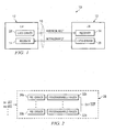
- FIGURE 1 illustrates one embodiment of a network element 10 for digital transmission between large-scale integration (LSI) integrated circuits (ICs) 12 having an LVDS driver 28 for high-speed digital transmission.
- network element 10 includes a plurality of LSI ICs 12.
- LSI ICs 12 include a receiver 14 and an LVDS driver 28 coupled by an interconnect 16.
- Receiver 14 receives packets from LVDS driver 28.
- Receiver 14 may include any suitable receiver.
- Reference to packets may include a packet, datagram, frame, or other unit of data.
- LVDS driver 28 drives differential signals for high-speed digital transmission from LSI IC 12.
- Interconnect 16 facilitates transmission of packets between LVDS driver 28 and receiver 14.
- Interconnect 16 may include any suitable element, such as a cable or a print circuit board trace.
- LVDS driver 28 is illustrated as being used in LSI IC 12 of network element 10, embodiments of the present invention may be used in any suitable network element in any suitable network or in any other appropriate application requiring digital signal transmission.
- FIGURE 2 illustrates a block diagram of LVDS driver 28 for providing a large output voltage swing and high-speed digital transmission.
- Traditional driver architectures have large internal capacitive loading. The large internal capacitive loading causes difficulty in meeting standards that require the large output voltage swing at lower transmission speeds and a lower output voltage swing at higher transmission speeds.
- LVDS driver 28 includes pre-drivers 30 and programmable fingers 32 and receives inputs IN1, IN1 , IN2, and IN2 .
- a programmable finger 32 may be associated with a pre-driver 30.
- pre-driver 30a is associated with programmable finger 32a
- pre-driver 30b is associated with programmable finger 32b.
- Pre-drivers 30 control the operation of the associated programmable finger 32.
- Programmable fingers 32 may be selectively engaged or disengaged from LVDS driver 28. Therefore, the number of engaged programmable fingers 32 may be used to control the total capacitive loading and maximum voltage swing provided by LVDS driver 28 (since each programmable finger 32 contributes to both the capacitive loading and to the maximum voltage swing).
- a lower number of programmable fingers 32 may be enabled to reduce the total capacitive loading. For example, at 10.4 Gigabits per second, the output amplitude is 300mV for a single-end circuit and 600 mV for a differential circuit. On the other hand, during low-speed transmission that has a higher required output voltage swing but less sensitivity to capacitive loading, a higher number of programmable fingers 32 may be enabled. For example, at 3.125 Gigabits per second, the output amplitude is 600mV for a single-end circuit and 1200mV for a differential circuit.
- LVDS driver 28 may include five programmable fingers 32, and different applications may require the operation of a different number of programmable fingers 32.
- Each of the pre-drivers 30 associated with the needed programmable fingers 32 enables the associated programmable fingers 32, and the remaining pre-drivers 30 disable their associated programmable fingers 32.
- two programmable fingers 32 may be turned on for 10G (ten Gigabits per second) operation and up to five programmable fingers 32 may be turned on for 3G operation (three Gigabits per second).
- LVDS driver 28 may operate at any suitable transmission speed for any suitable application.
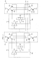
- FIGURE 3 illustrates an embodiment of a circuit-level diagram of the LVDS driver 28.
- LVDS driver 28 includes a pre-driver logic 40 and transistors 42.
- Pre-driver logic 40 may include any suitable component.
- each pre-driver 30 includes pre-driver logic 40.
- Programmable fingers 32 include transistors 42.
- programmable fingers 32 include p-channel metal-oxide semiconductor field effect transistors (PMOS transistors) as illustrated by transistors 42a, 42c, 42e, and 42g and an n-channel metal-oxide semiconductor field effect transistors (NMOS transistors) as illustrated by transistors 42b, 42d, 42f, and 42h.
- PMOS transistors p-channel metal-oxide semiconductor field effect transistors
- NMOS transistors n-channel metal-oxide semiconductor field effect transistors
- transistors 42a and 42c couple to a Direct Current (DC) voltage source (V DD ) and operate as a source-type current source.
- Transistors 42b and 42d couple to voltage source (V SS ) and operate as a sink-type current source.
- a cascode current mirror may be implemented to form the current source.
- Transistors 42e, 42f, 42g, and 42h operate as a complementary switch.
- Each programmable finger 32 may be completely enabled or disabled by their associated pre-driver 30 depending on the application. Providing a signal to pre-driver 30 at P D allows pre-driver 30 to control and enable programmable fingers 32.
- Y 1 and Z 1 are the same as A 1 and Y 2 and Z 2 are the same as A 2 .
- the values of A 1 and A 2 determine the values of Y 1 , Z 1 , Y 2 , and Z 2 .
- Y 1 and Y 2 have values equal to V DD and Z 1 and Z 2 have values equal to V SS .
- the following table illustrates the logic functions: P D A 1 A 2 Y 1 Y 2 Z 1 Z 2 0 0 1 0 1 0 1 0 1 0 1 0 1 0 1 0 1 X X 1 1 0 0 0
- programmable finger 32 When P D has a logic value of zero, programmable finger 32 is enabled. Alternatively, when P D has a logic value of one, regardless of the input signals A 1 and A 2 , programmable finger 32 is disabled.
- the above logic table is applicable to programmable finger 32b when enabled and disabled.
- programmable finger 32 When programmable finger 32 is disabled, the components in programmable finger 32 do not contribute any internal capacitive loading at output nodes, OUT and OUT .
- the output voltage swing depends on total currents added by active programmable fingers 32, the loading at the output nodes, and the switching PMOS and NMOS loading paths.
- pre-drivers 30 enable and disable the programmable fingers 32. Any suitable number of programmable fingers 32 are enabled or disabled to accommodate the requirements of an application.
- An input is provided at P D on pre-driver 30, which allows for control of associated programmable finger 32.
- P D 1
- P D 0 and input signals A 1 and A 2 have logic values of zero or one
- the application proceeds accordingly based on the configuration of enabled and disabled programmable fingers 32.
- the configuration of enabled and disabled programmable fingers 32 may change to facilitate another application.
- a total of disabled and enabled programmable fingers 32 is at least two programmable fingers 32.
Landscapes
- Engineering & Computer Science (AREA)
- Computer Hardware Design (AREA)
- Physics & Mathematics (AREA)
- Computing Systems (AREA)
- General Engineering & Computer Science (AREA)
- Mathematical Physics (AREA)
- Logic Circuits (AREA)
- Dc Digital Transmission (AREA)
Abstract
Description
- This invention relates generally to signal communication, and more specifically, to a low-voltage differential signal (LVDS) driver for high-speed digital transmission.
- Various Complementary Metal-Oxide Semiconductor (CMOS) driver architectures exist for high-speed digital transmission. The CMOS driver architectures have difficulty meeting standards that require large output amplitude swing and high speed in a single driver. The large internal capacitive loading contributes to this difficulty and additionally results in a large return loss.
- In accordance with the present invention, disadvantages and problems associated with previous techniques for providing a large output voltage swing at low transmission speeds and lower output voltage swing at high transmission speeds in a single driver may be reduced or eliminated.
- According to one embodiment of the present invention, a low-voltage differential signal (LVDS) driver includes at least two programmable fingers operable to drive a signal and at least two pre-drivers. Each pre-driver is associated with one programmable finger and is operable to enable or disable the associated programmable finger. An enabled programmable finger drives the signal and contributes to the capacitive loading of the driver, and a disabled programmable finger does not drive the signal and does not contribute to the capacitive loading of the driver.
- Certain embodiments of the invention may provide one or more technical advantages. A technical advantage of one embodiment includes supporting standards that require a large output amplitude swing and a high-speed data rates in a single driver. For example, a single LVDS driver supports a large output voltage swing at low transmission speeds and supports a lower output voltage swing at high transmission speeds. Another technical advantage of another embodiment includes using a selected number of programmable fingers for an application based on the requirements of the application. Configuring the appropriate number of programmable fingers for an application saves power. Adjusting the number of programmable fingers used in an application also improves return loss.
- Certain embodiments of the invention may include none, some, or all of the above technical advantages. One or more other technical advantages may be readily apparent to one skilled in the art from the figures, descriptions, and claims included herein.
- For a more complete understanding of the present invention and its features and advantages, reference is now made to the following description, taken in conjunction with the accompanying drawings, in which:
- FIGURE 1 illustrates one embodiment of a network element for digital transmission between large-scale integration integrated circuits having an LVDS driver for high-speed digital transmission;
- FIGURE 2 illustrates a block diagram of the LVDS driver for providing a large output voltage swing and high-speed digital transmission; and
- FIGURE 3 illustrates an embodiment of a circuit-level diagram of the LVDS driver.
- Embodiments of the present invention and its advantages are best understood by referring to FIGURES 1 through 3 of the drawings, like numerals being used for like and corresponding parts of the various drawings.
- FIGURE 1 illustrates one embodiment of a
network element 10 for digital transmission between large-scale integration (LSI) integrated circuits (ICs) 12 having anLVDS driver 28 for high-speed digital transmission. In the illustrated embodiment,network element 10 includes a plurality ofLSI ICs 12.LSI ICs 12 include areceiver 14 and anLVDS driver 28 coupled by aninterconnect 16.Receiver 14 receives packets from LVDSdriver 28.Receiver 14 may include any suitable receiver. Reference to packets may include a packet, datagram, frame, or other unit of data. LVDS driver 28 drives differential signals for high-speed digital transmission from LSI IC 12. Interconnect 16 facilitates transmission of packets between LVDSdriver 28 andreceiver 14. Interconnect 16 may include any suitable element, such as a cable or a print circuit board trace. - It should be noted that although LVDS
driver 28 is illustrated as being used in LSI IC 12 ofnetwork element 10, embodiments of the present invention may be used in any suitable network element in any suitable network or in any other appropriate application requiring digital signal transmission. - FIGURE 2 illustrates a block diagram of LVDS
driver 28 for providing a large output voltage swing and high-speed digital transmission. Traditional driver architectures have large internal capacitive loading. The large internal capacitive loading causes difficulty in meeting standards that require the large output voltage swing at lower transmission speeds and a lower output voltage swing at higher transmission speeds. - In the illustrated embodiment,
LVDS driver 28 includes pre-drivers 30 and programmable fingers 32 and receives inputs IN1,IN1 , IN2, andIN2 . A programmable finger 32 may be associated with a pre-driver 30. For example, pre-driver 30a is associated withprogrammable finger 32a, and pre-driver 30b is associated withprogrammable finger 32b. Pre-drivers 30 control the operation of the associated programmable finger 32. Programmable fingers 32 may be selectively engaged or disengaged from LVDSdriver 28. Therefore, the number of engaged programmable fingers 32 may be used to control the total capacitive loading and maximum voltage swing provided by LVDS driver 28 (since each programmable finger 32 contributes to both the capacitive loading and to the maximum voltage swing). For example, during high-speed transmission that has a lower required output voltage swing but more sensitivity to capacitive loading, a lower number of programmable fingers 32 may be enabled to reduce the total capacitive loading. For example, at 10.4 Gigabits per second, the output amplitude is 300mV for a single-end circuit and 600 mV for a differential circuit. On the other hand, during low-speed transmission that has a higher required output voltage swing but less sensitivity to capacitive loading, a higher number of programmable fingers 32 may be enabled. For example, at 3.125 Gigabits per second, the output amplitude is 600mV for a single-end circuit and 1200mV for a differential circuit. - As an example only, LVDS
driver 28 may include five programmable fingers 32, and different applications may require the operation of a different number of programmable fingers 32. Each of the pre-drivers 30 associated with the needed programmable fingers 32 enables the associated programmable fingers 32, and the remaining pre-drivers 30 disable their associated programmable fingers 32. For example, in a particular exemplary embodiment, two programmable fingers 32 may be turned on for 10G (ten Gigabits per second) operation and up to five programmable fingers 32 may be turned on for 3G operation (three Gigabits per second). LVDSdriver 28 may operate at any suitable transmission speed for any suitable application. - FIGURE 3 illustrates an embodiment of a circuit-level diagram of the LVDS
driver 28. In the illustrated embodiment, LVDSdriver 28 includes apre-driver logic 40 and transistors 42. Pre-driverlogic 40 may include any suitable component. In the illustrated embodiment, each pre-driver 30 includes pre-driverlogic 40. Programmable fingers 32 include transistors 42. In the illustrated embodiment, programmable fingers 32 include p-channel metal-oxide semiconductor field effect transistors (PMOS transistors) as illustrated bytransistors transistors - In the illustrated embodiment,
transistors Transistors 42b and 42d couple to voltage source (VSS) and operate as a sink-type current source. As another example, a cascode current mirror may be implemented to form the current source.Transistors - Each programmable finger 32 may be completely enabled or disabled by their associated pre-driver 30 depending on the application. Providing a signal to pre-driver 30 at PD allows pre-driver 30 to control and enable programmable fingers 32. When a selected
programmable finger 32a is enabled, Y1 and Z1 are the same as A1 and Y2 and Z2 are the same as A2. As indicated in the table below, the values of A1 and A2 determine the values of Y1, Z1, Y2, and Z2. When selectedprogrammable finger 32a is disabled, Y1 and Y2 have values equal to VDD and Z1 and Z2 have values equal to VSS. The following table illustrates the logic functions:P D A 1 A 2 Y 1 Y 2 Z 1 Z 2 0 0 1 0 1 0 1 0 1 0 1 0 1 0 1 X X 1 1 0 0 - When PD has a logic value of zero, programmable finger 32 is enabled. Alternatively, when PD has a logic value of one, regardless of the input signals A1 and A2, programmable finger 32 is disabled. The above logic table is applicable to
programmable finger 32b when enabled and disabled. When programmable finger 32 is disabled, the components in programmable finger 32 do not contribute any internal capacitive loading at output nodes, OUT andOUT . The output voltage swing depends on total currents added by active programmable fingers 32, the loading at the output nodes, and the switching PMOS and NMOS loading paths. - In operation, upon determining which programmable fingers 32 to enable and which programmable fingers 32 to disable, pre-drivers 30 enable and disable the programmable fingers 32. Any suitable number of programmable fingers 32 are enabled or disabled to accommodate the requirements of an application. An input is provided at PD on pre-driver 30, which allows for control of associated programmable finger 32. As described above, when PD=1, programmable finger 32 is disabled and Y1=Y2=VDD and Z1=Z2=VSS. As another example, when PD=0 and input signals A1 and A2 have logic values of zero or one, programmable finger 32 is enabled and Y1, Z1=A1 and Y2, Z2=A2. The application proceeds accordingly based on the configuration of enabled and disabled programmable fingers 32. The configuration of enabled and disabled programmable fingers 32 may change to facilitate another application. In an embodiment, a total of disabled and enabled programmable fingers 32 is at least two programmable fingers 32.
- Although the present invention has been described in several embodiments, a myriad of changes, variations, alterations, transformations, and modifications may be suggested to one skilled in the art, and it is intended that the present invention encompass such changes, variations, alterations, transformations, and modifications as fall within the scope of the appended claims.
Claims (19)
- A low-voltage differential signal (LVDS) driver, comprising:at least two programmable fingers operable to drive a signal; andat least two pre-drivers, each pre-driver associated with one programmable finger and operable to enable or disable the associated programmable finger, an enabled programmable finger driving the signal and contributing to the capacitive loading of the driver, and a disabled programmable finger not driving the signal and not contributing to the capacitive loading of the driver.
- The driver of Claim 1, wherein the at least two pre-drivers each comprises pre-driver logic.
- The driver of Claim 1, wherein the at least two programmable fingers each comprises a plurality of transistors, the plurality of transistors comprising a plurality of p-channel metal-oxide field effect transistors and a plurality of n-channel metal-oxide field effect transistors.
- The driver of Claim 1, comprising five programmable fingers and wherein only two of the programmable fingers are enabled to facilitate the transmission of the signal at a high speed, wherein the driver has a low output voltage swing.
- The driver of Claim 4, wherein the high speed transmission is greater than or equal to approximately ten Gigabits per second and the low output voltage swing of a differential circuit is less than or equal to approximately 600mV and the low output voltage swing of a single-end circuit is less than or equal to approximately 300mV.
- The driver of Claim 1, comprising five programmable fingers and wherein all five of the programmable fingers are enabled to facilitate the transmission of a signal at a low speed, wherein the driver has a high output voltage swing.
- The driver of Claim 6, wherein the low speed transmission is less than or equal to approximately three Gigabits per second and the high output voltage swing of a differential circuit is greater than or equal to approximately 1200mV and the high output voltage swing of a single-end circuit is greater than or equal to approximately 600mV.
- A method for driving a low-voltage differential signal (LVDS), comprising selectively enabling one or more programmable fingers of an LVDS driver, each programmable finger operable to drive a signal, an enabled programmable finger driving the signal and contributing to the capacitive loading of the driver, and a disabled programmable finger not driving the signal and not contributing to the capacitive loading of the driver.
- The method of Claim 8, wherein selectively enabling one or more programmable fingers comprises receiving a signal at PD of the driver.
- The method of Claim 8, wherein selectively enabling one or more programmable fingers comprises receiving an input having a logic value of zero or one.
- The method of Claim 8, wherein selectively enabling one or more programmable fingers comprises:enabling two programmable fingers to facilitate the transmission of the signal at a high speed; andhaving a low output voltage swing.
- The method of Claim 11, wherein the high speed transmission is greater than or equal to approximately ten Gigabits per second and the low output voltage swing of a differential circuit is less than or equal to approximately 600mV and the low output voltage swing of a single-end circuit is less than or equal to approximately 300mV.
- The method of Claim 8, wherein selectively enabling one or more programmable fingers comprises:enabling five programmable fingers to facilitate the transmission of the signal at a low speed; andhaving a high output voltage swing.
- The method of Claim 13, wherein the low speed transmission is less than or equal to approximately three Gigabits per second and the high output voltage swing of a differential circuit is greater than or equal to approximately 1200mV and the high output voltage swing of a single-end circuit is greater than or equal to approximately 600mV.
- A system for driving a low-voltage differential signal (LVDS), comprising:means for driving a signal; andmeans for selectively enabling one or more driving means of an LVDS driver, an enabled driving means driving the signal and contributing to the capacitive loading of the driver, and a disabled driving means not driving the signal and not contributing to the capacitive loading of the driver.
- The system of Claim 15, further comprising means for receiving a signal at PD of the driver.
- The system of Claim 15, further comprising means for receiving an input having a logic value of zero or one.
- The system of Claim 15, further comprising:means for driving the signal at a high speed; andmeans for having a low output voltage swing.
- The system of Claim 15, further comprising:means for driving the signal at a low speed; andmeans for having a high output voltage swing.
Applications Claiming Priority (1)
| Application Number | Priority Date | Filing Date | Title |
|---|---|---|---|
| US11/421,522 US7427878B2 (en) | 2006-06-01 | 2006-06-01 | Low-voltage differential signal driver for high-speed digital transmission |
Publications (2)
| Publication Number | Publication Date |
|---|---|
| EP1863178A2 true EP1863178A2 (en) | 2007-12-05 |
| EP1863178A3 EP1863178A3 (en) | 2016-11-02 |
Family
ID=38520760
Family Applications (1)
| Application Number | Title | Priority Date | Filing Date |
|---|---|---|---|
| EP07010780.0A Withdrawn EP1863178A3 (en) | 2006-06-01 | 2007-05-31 | Low-voltage differential signal driver for high-speed digital transmission |
Country Status (4)
| Country | Link |
|---|---|
| US (1) | US7427878B2 (en) |
| EP (1) | EP1863178A3 (en) |
| JP (1) | JP4992555B2 (en) |
| CN (1) | CN101106373A (en) |
Cited By (1)
| Publication number | Priority date | Publication date | Assignee | Title |
|---|---|---|---|---|
| CN101394377B (en) * | 2008-09-24 | 2011-06-08 | 硅谷数模半导体(北京)有限公司 | Pre-loading device and low voltage differential signal transmitter |
Families Citing this family (7)
| Publication number | Priority date | Publication date | Assignee | Title |
|---|---|---|---|---|
| JP4996517B2 (en) * | 2008-03-24 | 2012-08-08 | ルネサスエレクトロニクス株式会社 | Input circuit and semiconductor integrated circuit including the input circuit |
| US8270464B2 (en) * | 2008-06-20 | 2012-09-18 | Fujitsu Limited | Decision feedback equalizer (DFE) |
| US7902883B2 (en) * | 2008-06-20 | 2011-03-08 | Fujitsu Limited | Preemphasis driver with replica bias |
| US8213494B2 (en) * | 2008-06-20 | 2012-07-03 | Fujitsu Limited | Sign-based general zero-forcing adaptive equalizer control |
| US8008944B2 (en) * | 2008-11-25 | 2011-08-30 | Qualcomm Incorporated | Low voltage differential signaling driver with programmable on-chip resistor termination |
| US9065399B2 (en) * | 2013-06-14 | 2015-06-23 | Altera Corporation | Programmable high-speed voltage-mode differential driver |
| CN106849935A (en) * | 2016-12-23 | 2017-06-13 | 深圳市国微电子有限公司 | A kind of clock buffer drive circuit and PLD |
Citations (1)
| Publication number | Priority date | Publication date | Assignee | Title |
|---|---|---|---|---|
| US6081142A (en) * | 1997-05-14 | 2000-06-27 | Fujitsu Limited | Hold time margin increased semiconductor device and access time adjusting method for same |
Family Cites Families (20)
| Publication number | Priority date | Publication date | Assignee | Title |
|---|---|---|---|---|
| JP3003577B2 (en) * | 1996-07-19 | 2000-01-31 | 日本電気株式会社 | Semiconductor integrated circuit |
| US5977796A (en) * | 1997-06-26 | 1999-11-02 | Lucent Technologies, Inc. | Low voltage differential swing interconnect buffer circuit |
| US6111431A (en) | 1998-05-14 | 2000-08-29 | National Semiconductor Corporation | LVDS driver for backplane applications |
| JP2000031810A (en) | 1998-07-10 | 2000-01-28 | Fujitsu Ltd | Driver circuit |
| JP4199377B2 (en) * | 1999-06-16 | 2008-12-17 | 富士通マイクロエレクトロニクス株式会社 | LSI devices |
| US6353334B1 (en) | 2000-01-27 | 2002-03-05 | Xilinx, Inc. | Circuit for converting a logic signal on an output node to a pair of low-voltage differential signals |
| US6262606B1 (en) * | 2000-08-04 | 2001-07-17 | Dolphin Technology, Inc. | Waveform compensated output driver |
| US6366128B1 (en) * | 2000-09-05 | 2002-04-02 | Xilinx, Inc. | Circuit for producing low-voltage differential signals |
| JP2002152032A (en) * | 2000-11-16 | 2002-05-24 | Hitachi Ltd | Output circuit and semiconductor integrated circuit |
| US6650140B2 (en) | 2001-03-19 | 2003-11-18 | Altera Corporation | Programmable logic device with high speed serial interface circuitry |
| US6836149B2 (en) | 2002-04-12 | 2004-12-28 | Stmicroelectronics, Inc. | Versatile RSDS-LVDS-miniLVDS-BLVDS differential signal interface circuit |
| US6990644B2 (en) | 2002-04-18 | 2006-01-24 | International Business Machines Corporation | On chip timing adjustment in multi-channel fast data transfer |
| US6831480B1 (en) * | 2003-01-07 | 2004-12-14 | Altera Corporation | Programmable logic device multispeed I/O circuitry |
| JP4205969B2 (en) * | 2003-02-18 | 2009-01-07 | パナソニック株式会社 | Current driver circuit |
| US7236013B2 (en) * | 2003-12-26 | 2007-06-26 | Stmicroelectronics Pvt. Ltd. | Configurable output buffer and method to provide differential drive |
| JP2005217999A (en) * | 2004-02-02 | 2005-08-11 | Hitachi Ltd | Digital data transmission circuit |
| US7145359B2 (en) * | 2004-06-28 | 2006-12-05 | Silicon Laboratories Inc. | Multiple signal format output buffer |
| KR100555571B1 (en) * | 2004-09-07 | 2006-03-03 | 삼성전자주식회사 | Transmitter of semiconductor device |
| US7268623B2 (en) | 2004-12-10 | 2007-09-11 | Electronics And Telecommunications Research Institute | Low voltage differential signal driver circuit and method for controlling the same |
| US20070013411A1 (en) * | 2005-07-14 | 2007-01-18 | Kazi Asaduzzaman | Apparatus and methods for programmable slew rate control in transmitter circuits |
-
2006
- 2006-06-01 US US11/421,522 patent/US7427878B2/en not_active Expired - Fee Related
-
2007
- 2007-05-31 EP EP07010780.0A patent/EP1863178A3/en not_active Withdrawn
- 2007-05-31 JP JP2007145951A patent/JP4992555B2/en not_active Expired - Fee Related
- 2007-05-31 CN CNA2007101054649A patent/CN101106373A/en active Pending
Patent Citations (1)
| Publication number | Priority date | Publication date | Assignee | Title |
|---|---|---|---|---|
| US6081142A (en) * | 1997-05-14 | 2000-06-27 | Fujitsu Limited | Hold time margin increased semiconductor device and access time adjusting method for same |
Cited By (1)
| Publication number | Priority date | Publication date | Assignee | Title |
|---|---|---|---|---|
| CN101394377B (en) * | 2008-09-24 | 2011-06-08 | 硅谷数模半导体(北京)有限公司 | Pre-loading device and low voltage differential signal transmitter |
Also Published As
| Publication number | Publication date |
|---|---|
| US7427878B2 (en) | 2008-09-23 |
| EP1863178A3 (en) | 2016-11-02 |
| CN101106373A (en) | 2008-01-16 |
| JP4992555B2 (en) | 2012-08-08 |
| US20070279098A1 (en) | 2007-12-06 |
| JP2007325272A (en) | 2007-12-13 |
Similar Documents
| Publication | Publication Date | Title |
|---|---|---|
| EP1863178A2 (en) | Low-voltage differential signal driver for high-speed digital transmission | |
| US6531892B2 (en) | Bias voltage generator usable with circuit for producing low-voltage differential signals | |
| US7940086B2 (en) | Interface circuit that can switch between single-ended transmission and differential transmission | |
| EP3001564B1 (en) | Controller area network bus transmitter with complementary source follower driver | |
| US20070013411A1 (en) | Apparatus and methods for programmable slew rate control in transmitter circuits | |
| EP0449251A2 (en) | Output circuit | |
| US9350337B2 (en) | Clamp circuit and method for clamping voltage | |
| US20080054953A1 (en) | RSDS/LVDS Driving Circuits Suitable for Low Working Voltages | |
| CN102754347B (en) | Low power high-speed differential driver with precision current steering | |
| US6580292B2 (en) | Universal PECL/LVDS output structure | |
| US20230229620A1 (en) | Apparatus and methods for high-speed drivers | |
| CN115065358A (en) | IO driving circuit and chip | |
| US6496044B1 (en) | High-speed output circuit with low voltage capability | |
| CN101146069A (en) | Differential signal driving circuit applicable to low working voltage | |
| EP2464009B1 (en) | Differential signal termination circuit | |
| US7138822B2 (en) | Integrated circuit and method of improving signal integrity | |
| CN112751549B (en) | High-speed LVDS resistance state control circuit and control method | |
| US7521964B1 (en) | High-speed level-shifting circuit | |
| JP4107984B2 (en) | Multi-input CMOS gate circuit | |
| JP2779226B2 (en) | Bi-CMOS output circuit | |
| KR100788221B1 (en) | Output Buffer Circuit with Deemphasis | |
| US20060125526A1 (en) | Differential analog logic circuit with symmetric inputs and output | |
| JP2006191417A (en) | Output buffer circuit |
Legal Events
| Date | Code | Title | Description |
|---|---|---|---|
| PUAI | Public reference made under article 153(3) epc to a published international application that has entered the european phase |
Free format text: ORIGINAL CODE: 0009012 |
|
| AK | Designated contracting states |
Kind code of ref document: A2 Designated state(s): AT BE BG CH CY CZ DE DK EE ES FI FR GB GR HU IE IS IT LI LT LU LV MC MT NL PL PT RO SE SI SK TR |
|
| AX | Request for extension of the european patent |
Extension state: AL BA HR MK YU |
|
| RIC1 | Information provided on ipc code assigned before grant |
Ipc: H03K 19/0175 20060101AFI20160621BHEP Ipc: H03K 19/0185 20060101ALI20160621BHEP |
|
| PUAL | Search report despatched |
Free format text: ORIGINAL CODE: 0009013 |
|
| AK | Designated contracting states |
Kind code of ref document: A3 Designated state(s): AT BE BG CH CY CZ DE DK EE ES FI FR GB GR HU IE IS IT LI LT LU LV MC MT NL PL PT RO SE SI SK TR |
|
| AX | Request for extension of the european patent |
Extension state: AL BA HR MK RS |
|
| RIC1 | Information provided on ipc code assigned before grant |
Ipc: H03K 19/0185 20060101ALI20160927BHEP Ipc: H03K 19/0175 20060101AFI20160927BHEP |
|
| 17P | Request for examination filed |
Effective date: 20170425 |
|
| RBV | Designated contracting states (corrected) |
Designated state(s): AT BE BG CH CY CZ DE DK EE ES FI FR GB GR HU IE IS IT LI LT LU LV MC MT NL PL PT RO SE SI SK TR |
|
| AKX | Designation fees paid |
Designated state(s): DE FR GB |
|
| AXX | Extension fees paid |
Extension state: MK Extension state: RS Extension state: AL Extension state: HR Extension state: BA |
|
| 17Q | First examination report despatched |
Effective date: 20180308 |
|
| GRAP | Despatch of communication of intention to grant a patent |
Free format text: ORIGINAL CODE: EPIDOSNIGR1 |
|
| INTG | Intention to grant announced |
Effective date: 20190719 |
|
| STAA | Information on the status of an ep patent application or granted ep patent |
Free format text: STATUS: THE APPLICATION IS DEEMED TO BE WITHDRAWN |
|
| 18D | Application deemed to be withdrawn |
Effective date: 20191130 |