EP1863075A1 - Group iii nitride semiconductor device and epitaxial substrate - Google Patents
Group iii nitride semiconductor device and epitaxial substrate Download PDFInfo
- Publication number
- EP1863075A1 EP1863075A1 EP06715282A EP06715282A EP1863075A1 EP 1863075 A1 EP1863075 A1 EP 1863075A1 EP 06715282 A EP06715282 A EP 06715282A EP 06715282 A EP06715282 A EP 06715282A EP 1863075 A1 EP1863075 A1 EP 1863075A1
- Authority
- EP
- European Patent Office
- Prior art keywords
- epitaxial
- substrate
- gallium nitride
- algan
- epitaxial layer
- Prior art date
- Legal status (The legal status is an assumption and is not a legal conclusion. Google has not performed a legal analysis and makes no representation as to the accuracy of the status listed.)
- Ceased
Links
Images




Classifications
-
- H—ELECTRICITY
- H10—SEMICONDUCTOR DEVICES; ELECTRIC SOLID-STATE DEVICES NOT OTHERWISE PROVIDED FOR
- H10D—INORGANIC ELECTRIC SEMICONDUCTOR DEVICES
- H10D30/00—Field-effect transistors [FET]
- H10D30/40—FETs having zero-dimensional [0D], one-dimensional [1D] or two-dimensional [2D] charge carrier gas channels
- H10D30/47—FETs having zero-dimensional [0D], one-dimensional [1D] or two-dimensional [2D] charge carrier gas channels having two-dimensional [2D] charge carrier gas channels, e.g. nanoribbon FETs or high electron mobility transistors [HEMT]
- H10D30/471—High electron mobility transistors [HEMT] or high hole mobility transistors [HHMT]
- H10D30/475—High electron mobility transistors [HEMT] or high hole mobility transistors [HHMT] having wider bandgap layer formed on top of lower bandgap active layer, e.g. undoped barrier HEMTs such as i-AlGaN/GaN HEMTs
- H10D30/4755—High electron mobility transistors [HEMT] or high hole mobility transistors [HHMT] having wider bandgap layer formed on top of lower bandgap active layer, e.g. undoped barrier HEMTs such as i-AlGaN/GaN HEMTs having wide bandgap charge-carrier supplying layers, e.g. modulation doped HEMTs such as n-AlGaAs/GaAs HEMTs
-
- H—ELECTRICITY
- H10—SEMICONDUCTOR DEVICES; ELECTRIC SOLID-STATE DEVICES NOT OTHERWISE PROVIDED FOR
- H10P—GENERIC PROCESSES OR APPARATUS FOR THE MANUFACTURE OR TREATMENT OF DEVICES COVERED BY CLASS H10
- H10P10/00—Bonding of wafers, substrates or parts of devices
-
- H—ELECTRICITY
- H10—SEMICONDUCTOR DEVICES; ELECTRIC SOLID-STATE DEVICES NOT OTHERWISE PROVIDED FOR
- H10D—INORGANIC ELECTRIC SEMICONDUCTOR DEVICES
- H10D62/00—Semiconductor bodies, or regions thereof, of devices having potential barriers
- H10D62/80—Semiconductor bodies, or regions thereof, of devices having potential barriers characterised by the materials
- H10D62/85—Semiconductor bodies, or regions thereof, of devices having potential barriers characterised by the materials being Group III-V materials, e.g. GaAs
- H10D62/8503—Nitride Group III-V materials, e.g. AlN or GaN
-
- H—ELECTRICITY
- H10—SEMICONDUCTOR DEVICES; ELECTRIC SOLID-STATE DEVICES NOT OTHERWISE PROVIDED FOR
- H10P—GENERIC PROCESSES OR APPARATUS FOR THE MANUFACTURE OR TREATMENT OF DEVICES COVERED BY CLASS H10
- H10P14/00—Formation of materials, e.g. in the shape of layers or pillars
- H10P14/20—Formation of materials, e.g. in the shape of layers or pillars of semiconductor materials
- H10P14/29—Formation of materials, e.g. in the shape of layers or pillars of semiconductor materials characterised by the substrates
- H10P14/2901—Materials
- H10P14/2907—Materials being Group IIIA-VA materials
- H10P14/2908—Nitrides
-
- H—ELECTRICITY
- H10—SEMICONDUCTOR DEVICES; ELECTRIC SOLID-STATE DEVICES NOT OTHERWISE PROVIDED FOR
- H10P—GENERIC PROCESSES OR APPARATUS FOR THE MANUFACTURE OR TREATMENT OF DEVICES COVERED BY CLASS H10
- H10P14/00—Formation of materials, e.g. in the shape of layers or pillars
- H10P14/20—Formation of materials, e.g. in the shape of layers or pillars of semiconductor materials
- H10P14/32—Formation of materials, e.g. in the shape of layers or pillars of semiconductor materials characterised by intermediate layers between substrates and deposited layers
- H10P14/3202—Materials thereof
- H10P14/3214—Materials thereof being Group IIIA-VA semiconductors
- H10P14/3216—Nitrides
-
- H—ELECTRICITY
- H10—SEMICONDUCTOR DEVICES; ELECTRIC SOLID-STATE DEVICES NOT OTHERWISE PROVIDED FOR
- H10P—GENERIC PROCESSES OR APPARATUS FOR THE MANUFACTURE OR TREATMENT OF DEVICES COVERED BY CLASS H10
- H10P14/00—Formation of materials, e.g. in the shape of layers or pillars
- H10P14/20—Formation of materials, e.g. in the shape of layers or pillars of semiconductor materials
- H10P14/34—Deposited materials, e.g. layers
- H10P14/3402—Deposited materials, e.g. layers characterised by the chemical composition
- H10P14/3414—Deposited materials, e.g. layers characterised by the chemical composition being group IIIA-VIA materials
- H10P14/3416—Nitrides
Definitions
- the present invention relates to Group III nitride semiconductor devices and epitaxial substrates.
- Non-Patent Document 1 high electron mobility transistors (HEMT) are disclosed.
- the high electron mobility transistors have an AlGaN/GaN heterostructure epitaxially grown on a sapphire substrate.
- an i -type GaN layer of 2 to 3 ⁇ m is formed.
- an i -type AlGaN layer of 7 nm, an n-type AlGaN layer of 15 nm, and an i -type AlGaN layer of 3 nm are formed in that order.
- the Schottky electrode is composed of Ni(3 nm)/Pt(300 nm)/Au(300 nm).
- Non-Patent Document 1 " Improvement of DC Characteristics of AlGaN/GaN High Electron Mobility Transistors Thermally Annealed Ni/Pt/Au Schottky Gate” Japanese Journal of Applied Physics Vol. 43, No. 4B, 2004, pp.1925-1929 .
- High electron mobility transistors manufactured by conventional technology are provided with a GaN layer and an AlGaN layer on a supporting body of sapphire.
- a Schottky gate is formed on the episurface of the AlGaN layer.
- the withstand voltage between the gate and the drain is low, such that the enhanced output power that is the goal is not attained. The reason for this is thought to be due to the larger leakage current from the gate electrode.
- numerous screw dislocations are present in the AlGaN film. If the gate electrode is fabricated on the surface of the AlGaN film the Schottky barrier is lowered due to the interface state originating in the screw dislocations. As a result, the leakage current from the gate electrode becomes large.
- the inventors have conducted various experiments in order to investigate which kind of crystal quality of the AlGaN film is related to the leakage current from the gate electrode.
- An object of the present invention brought about taking the above-described circumstances into consideration, is to make available Group III nitride semiconductor devices in which the leakage current from the Schottky electrode can be reduced, and meanwhile an object is to make available epitaxial substrates for manufacturing the Group III nitride semiconductor devices.
- the Group III nitride semiconductor device is furnished with (a) a supporting substrate composed of Al x Ga 1- x N (0 ⁇ x ⁇ 1), (b) an Al y Ga 1- y N epitaxial layer (0 ⁇ y ⁇ 1) having a full-width-at-half maximum for (0002) plane XRD of 150 sec or less, (c) a GaN epitaxial layer provided between the supporting substrate and the Al y Ga 1- y N epitaxial layer, (d) a Schottky electrode provided on the Al y Ga 1- y N epitaxial layer, (e) a source electrode provided on the gallium nitride epitaxial layer, and (f) a drain electrode provided on the gallium nitride epitaxial layer.
- the leakage current from the Schottky electrode in contact with the Al y Ga 1- y N epitaxial layer (0 ⁇ y ⁇ 1) is related to the full-width-at-half maximum for (0002) plane XRD.
- the full-width-at-half maximum for (0002) plane XRD is 150 sec or less, the leakage current from the Schottky electrode can be reduced.
- aluminum mole fraction y of the Al y Ga 1- y N epitaxial layer be between 0.1 and 0.7, inclusive.
- the band offset becomes small so that two-dimensional electron gas having enough density at the AlGaN/GaN interface is not formed. If the aluminum mole fraction y is more than 0.7, it is highly likely that cracks are generated in the AlGaN layer. The generation of the cracks prevents the two-dimensional electron gas from being formed at the AlGaN/GaN interface.
- the Al y Ga 1- y N epitaxial layer has a thickness between 5 nm and 50 nm, inclusive.
- the thickness of the Al y Ga 1- y N epitaxial layer is less than 5 nm, the distortion at the AlGaN/GaN interface becomes small so that the two-dimensional electron gas can not be formed. If the thickness of the Al y Ga 1- y N epitaxial layer is more than 50 nm, it is highly likely that the cracks are generated in the AlGaN layer. The generation of the cracks prevents the two-dimensional electron gas from being formed at the AlGaN/GaN interface.
- the supporting substrate be composed of gallium nitride.
- a Group III nitride semiconductor device can be provided using a supporting substrate having a low dislocation density.
- a separate aspect of the present invention involves an epitaxial substrate for a Group III nitride semiconductor device.
- the epitaxial substrate is furnished with (a) a substrate composed of Al x Ga 1- x N (0 ⁇ x ⁇ 1), (b) an Al y Ga 1- y N epitaxial film (0 ⁇ y ⁇ 1) having a full width at half maximum for (0002) plane XRD of 150 sec or less, and (c) a gallium nitride epitaxial film provided between the substrate and the Al y Ga 1- y N epitaxial film.
- the leakage current from the Schottky electrode in contact with the Al y Ga 1- y N epitaxial film (0 ⁇ y ⁇ 1) is related to the full width at half maximum for (0002) plane XRD.
- the full width at half maximum for (0002) plane XRD is 150 sec or less, the leakage current from the Schottky electrode formed on the Al y Ga 1- y N epitaxial film is small. Consequently, for example, epitaxial substrates preferably for high electron mobility transistors can be provided.
- aluminum composition y of the Al y Ga 1- y N epitaxial film be between 0.1 and 0.7, inclusive.
- the band offset becomes small so that two-dimensional electron gas having enough density at the AlGaN/GaN interface is not formed. If the aluminum mole fraction y of the Al y Ga 1- y N epitaxial film is more than 0.7, it is highly likely that cracks are generated in the AlGaN layer. The generation of the cracks prevents the two-dimensional electron gas from being formed at the AlGaN/GaN interface.
- the Al y Ga 1- y N epitaxial film has a thickness between 5 nm and 50 nm, inclusive.
- the thickness of the Al y Ga 1- y N epitaxial layer is less than 5 nm, the distortion at the AlGaN/GaN interface becomes small so that the two-dimensional electron gas can not be formed. If the thickness of the Al y Ga 1- y N epitaxial layer is more than 50 nm, it is highly likely that the cracks are generated in the AlGaN layer. The generation of the cracks prevents the two-dimensional electron gas from being formed at the AlGaN/GaN interface.
- the substrate be a gallium nitride substrate.
- an epitaxial substrate can be provided for a Group III nitride semiconductor device using a substrate having a low dislocation density.
- the present invention affords a Group III nitride semiconductor device in which the leakage current from the Schottky electrode is decreased. Furthermore, the present invention affords an epitaxial substrate for manufacturing the Group III nitride semiconductor device.
- Fig. 1 is a view representing a high electron mobility transistor involving Embodiment Mode 1.
- the high electron mobility transistor 11 is furnished with a supporting substrate 13, an Al y Ga 1- y N epitaxial layer (0 ⁇ y ⁇ 1) 15, a GaN epitaxial layer 17, a Schottky electrode 19, a source electrode 21, and a drain electrode 23.
- the supporting substrate 13 is composed of Al x Ga 1- x N (0 ⁇ x ⁇ 1), more specifically, AlN, AlGaN, or GaN.
- the Al y Ga 1- y N epitaxial layer 15 has a full-width-at-half maximum for (0002) plane XRD of 150 sec or less.
- the GaN epitaxial layer 17 is provided between the gallium nitride supporting substrate 13 and the Al y Ga 1- y N epitaxial layer 15.
- the Schottky electrode 19 is provided on the Al y Ga 1- y N epitaxial layer 15.
- the source electrode 21 and the drain electrode 23 are provided on the GaN epitaxial layer 17.
- the source electrode 21 may be provided on the Al y Ga 1- y N epitaxial layer 15.
- the drain electrode 23 may be provided on the Al y Ga 1- y N epitaxial layer 15.
- the source electrode 21 is in contact with the Al y Ga 1- y N epitaxial layer 15, and the drain electrode 23 is in contact with the Al y Ga 1- y N epitaxial layer 15.
- the Schottky electrode 19 constitutes a gate electrode of the high electron mobility transistor 11.
- the leakage current from the Schottky electrode 19 in contact with the Al y Ga 1- y N epitaxial layer 15 is related to the full-width-at-half maximum for (0002) plane XRD. Since the full-width-at-half maximum for (0002) plane XRD is 150 sec or less, the leakage current from the Schottky electrode 19 can reduced.
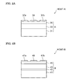
- Fig. 2A is a view representing structures of a high electron mobility transistor (HEMT) involving Embodiment Example.
- Fig. 2B is a view representing structures of an HEMT involving Experiment.
- HEMT high electron mobility transistor
- a gallium nitride substrate 31 is placed in a reactor of an MOVPE device. Supplying gases including hydrogen, nitrogen, and ammonia into the reactor, the gallium nitride substrate 31 undergoes a heat treatment at 1100 degrees Celsius for 20 minutes. Next, the temperature of the gallium nitride substrate 31 is increased to 1130 degrees Celsius. Ammonia and trimethylgallium (TMG) are supplied to the reactor to grow a gallium nitride film 33 having a thickness of 1.5 ⁇ m on the gallium nitride substrate 31. Trimethyl aluminum (TMA), TMG, and ammonia are supplied into the reactor to grow an AlGaN film 35 of 30 nm on the gallium nitride film 33.
- TMG trimethylgallium
- an epitaxial substrate A is manufactured.
- a source electrode 37a and a drain electrode 37b of Ti/A1/Ti/Au are formed on a surface of the epitaxial substrate A, and a gate electrode 39 of Au/Ni is formed on the surface of the epitaxial substrate A.
- an HEMT-A shown in Fig. 2A is manufactured.
- a sapphire substrate 41 is placed in a reactor of the MOVPE device. Supplying the gases including hydrogen, nitrogen, and ammonia into the reactor, the sapphire substrate 41 undergoes a heat treatment at a temperature of 1170 degrees Celsius for 10 minutes.
- a seed layer 42 is grown on the sapphire substrate 41.
- a gallium nitride film 43 and an AlGaN film 45 are grown to manufacture an epitaxial substrate B.
- a source electrode 47a and a drain electrode 47b of Ti/Al/Ti/Au are formed on the surface of the epitaxial substrate B, and a gate electrode 49 of Au/Ni is formed on the surface of the epitaxial substrate B.
- Fig. 3 is a view representing a spectrum for (0002) plane XRD in the surfaces of the AlGaN layers of the epitaxial substrate (sample A) and the epitaxial substrate (sample B) manufactured for the high electron mobility transistors.
- the sample A includes a GaN film and an AlGaN film formed on the gallium nitride substrate in this order.
- the sample B includes a seed film, a GaN film and an AlGaN film formed on the sapphire substrate in this order.
- a Schottky electrode is provided to measure the leakage current.
- the Schottky electrode has an area of 7.85 ⁇ 10 -5 cm 2 , and the applied voltage is -5 volts, for example.
- the leakage current in the sample A is largely reduced compared to the leakage current in the sample B.
- the reason is that as far as XRD of the AlGaN layer is concerned, FWHM of the sample A is more acute than that of the sample B.
- the XRD in the (0002) plane has a wider full-width-at-half maximum as the number of the screw dislocations included in the AlGaN layer is larger. Therefore, by making the full-width-at-half maximum small, the leakage current from the Schottky electrode can be reduced.
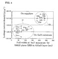
- the forward current through the gate electrode of the HEMT is about 0.1 A/cm -2 , therefore, it is necessary to limit the leakage current to 1 ⁇ 10 -4 A/cm 2 , 1/1000 of the forward current or less. As shown in Fig.
- the leakage current can be 1 ⁇ 10 -4 A/cm 2 or less.
- (0002) plane is preferable for evaluating the crystal quality of the AlGaN layer because (0002) plane has the great XRD strength.
- Fig. 4 is a view representing correspondences between leakage current density and the full-width-at-half maximum for (0002) plane XRD characteristic in the gallium nitride layer.
- Symbols indicated by reference marks 51a through 51h represent values obtained by measuring structures in which Schottky electrodes are manufactured on the AlGaN layer fabricated by utilizing the gallium nitride substrate.
- Symbols indicated by reference marks 53a through 53f represent values obtained by measuring structures in which Schottky electrodes are formed on the AlGaN layers fabricated by utilizing the sapphire substrates.
- a supporting substrate 13 of nitride is composed of gallium nitride conductive or semi-insulating.
- the gallium nitride region is homoepitaxially grown on the gallium nitride supporting substrate.
- the gallium nitride supporting substrate has a carrier concentration of 1 ⁇ 10 19 cm -3 or less.
- the GaN layer 17 has a thickness between 0.1 ⁇ m and 1000 ⁇ m, inclusive.
- the GaN layer 17 has a carrier concentration of 1 ⁇ 10 17 cm -3 or less.
- the AlGaN layer 15 has a thickness between 5 nm and 50 nm, inclusive.
- the AlGaN layer 15 has a carrier concentration of 1 ⁇ 10 19 cm -3 or less.
- aluminum composition Y of the Al y Ga 1- y N epitaxial layer 15 is preferably 0.1 or more. If the aluminum composition Y is less than 0.1, the band offset becomes small so that two-dimensional electron gas having enough density can not be formed at the AlGaN/GaN interface. Furthermore, the aluminum composition Y is preferably 0.7 or less. If the aluminum composition Y is more than 0.7, it is highly likely that cracks are generated in the AlGaN layer. The generation of the cracks prevents the two-dimensional electron gas from being formed at the AlGaN/GaN interface.
- the Al y Ga 1- y N epitaxial layer 15 preferably has a thickness of 5 nm or more. If the thickness of the Al y Ga 1- y N epitaxial layer 15 is less than 5 nm, the distortion at the AlGaN/GaN interface becomes small and the two-dimensional electron gas is not formed. Furthermore, the Al y Ga 1- y N epitaxial layer 15 preferably has a thickness of 50 nm or less. If the thickness of the Al y Ga 1- y N epitaxial layer is more than 50 nm, it is highly likely that the cracks are generated in the AlGaN layer. The generation of cracks prevents the two-dimensional electron gas from being formed at the AlGaN/GaN interface.
- the Al x Ga 1- x N supporting substrate for the high electron mobility transistor 11 is preferably composed of gallium nitride. Accordingly, Group III nitride semiconductor devices are provided using a supporting substrate of a low dislocation density.
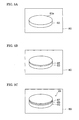
- Fig. 5A, Fig. 5B, and Fig. 5C are views representing manufacture of the epitaxial substrate according to Embodiment Mode 2.
- a gallium nitride freestanding substrate 83 having conductivity is placed in a reactor 80.
- the following crystal growth is preferably performed by MOVPE method.
- the gallium nitride freestanding substrate 83 has a carrier concentration of 1 ⁇ 10 19 cm -3 or less.
- a GaN epitaxial film 85 is deposited on a first surface 83a of the gallium nitride freestanding substrate 83.
- the GaN epitaxial film 85 is preferably undoped.
- the GaN epitaxial film 85 is deposited at a temperature between 600 degrees Celsius and 1200 degrees Celsius, inclusive.
- the pressure in the reactor is between 1 kPa and 120 kPa, inclusive.
- the gallium nitride epitaxial film 85 has a thickness between 0.5 ⁇ m and 1000 ⁇ m, inclusive.
- the GaN epitaxial film 85 has a carrier concentration of 1 ⁇ 10 17 cm -3 or less. If necessary, in advance of the growth of the GaN epitaxial film 85, a buffer layer can be grown.
- the buffer layer may be composed of any of AIN, GaN, AlGaN, InGaN, and AlInGaN.
- the buffer layer restrains defects or impurities of the gallium nitride freestanding substrate 83 from affecting the GaN epitaxial layer 85, so that quality of the GaN epitaxial layer 85 can be improved.
- TMA, TMG and NH 3 are supplied to deposit an undoped or n-type AlGaN epitaxial film 87 onto the undoped GaN epitaxial film 85.
- the AlGaN epitaxial film 87 is deposited at a temperature between 600 degrees Celsius and 1200 degrees Celsius, inclusive.
- the pressure in the reactor is between 1 kPa and 120 kPa, inclusive.
- the aluminum composition of the AlGaN epitaxial film 87 is between 0.1 and 0.7, inclusive.
- the AlGaN epitaxial film 87 has a thickness of 5 nm and 50 nm, inclusive.
- the AlGaN epitaxial film 87 has a carrier concentration of 1 ⁇ 10 19 cm -3 or less. Accordingly, an epitaxial substrate 81 is obtained. By making use of this substrate, an HEMT according to Embodiment Mode 1 can be manufactured.
- the inventors have found that the leakage current from the Schottky electrode in contact with the Al y Ga 1- y N epitaxial film 87 (0 ⁇ y ⁇ 1) is related to the full-width-at-half maximum for (0002) plane XRD.
- the leakage current from the Schottky electrode formed on the Al y Ga 1- y N epitaxial is small. Accordingly, an epitaxial substrate preferable for the high electron mobility transistor can be provided, for example.
- the full-width-at-half maximum for (0002) plane XRD is 150 sec or less, as apparent from Fig. 4, it is possible to reduce the leakage current from the Schottky electrode compared to a case of 150 sec or more.
- a Schottky electrode film for a gate electrode and ohmic electrode films for a source electrode and a drain electrode are deposited on a surface of the AlGaN epitaxial film 87 of the epitaxial substrate 81.
- the Schottky electrode and the ohmic electrode are formed from the Schottky electrode film and the ohmic electrode film, respectively.
- a Schottky electrode may be formed on the portion. Accordingly, it is possible to reduce the source resistance, improve the mutual conductance, and perform normally off. Furthermore, by adding n-type dopant, an n-type semiconductor region may be formed immediately under the source electrode and/or the drain electrode.
- n-type semiconductor regions to which n-type dopant is added may be grown as contact layers on the surface of the AlGaN epitaxial film 87, and on the contact layers a source electrode and/or a drain electrode may be formed. Accordingly, the contact resistance can be reduced. Furthermore, after thinning a portion of the AlGaN layer, a source and/or a drain electrode may be formed on the portion. Accordingly, the contact resistance can be reduced. Alternatively, the source and/or drain electrode may be formed to be in contact with the GaN layer having a band gap smaller than that of AlGaN by removing the AlGaN layer. Accordingly, the contact resistance can be reduced.
- an epitaxial substrate can be provided for semiconductor devices in which the backward leak current flowing through the Schottky junction when a voltage is applied across the Schottky electrode and the ohmic electrode can be reduced.
- Fig. 6 is a view representing one example of locations of high dislocation regions and low dislocation regions in a gallium nitride freestanding substrate for Embodiment Modes 1 and 2.
- a first surface 82a of the gallium nitride freestanding substrate 82 for the epitaxial substrate 81 includes first areas where high dislocation regions 82c having a relatively large screw dislocation density appear, and a second area where a low dislocation region 82d having a relatively small screw dislocation density appears.
- the high dislocation regions 82c are surrounded by the low dislocation region 82d, and the first areas are randomly distributed in a dot-like pattern in the second area on the first surface 82a.
- the screw dislocation density is 1 ⁇ 10 8 cm -2 or less, for example.
- the epitaxial substrate 81 gives an epitaxial layer having a lowered dislocation density in the low dislocation region 82d. Consequently, the backward leak current is reduced and the backward breakdown voltage is improved.
- Fig. 7 is a view representing another example of locations of the high dislocation regions and the low dislocation regions in a gallium nitride freestanding substrate for Embodiment Modes 1 and 2.
- a first surface 84a of the gallium nitride freestanding substrate 84 for the epitaxial substrate 81 includes first areas where high dislocation regions 84c having a relatively large screw dislocation density appear, and second areas where low dislocation regions 84d having a relatively small screw dislocation density appear.
- the high dislocation regions 84c are surrounded by the low dislocation regions 84d, and the first areas are distributed in a striped pattern in the second area on the first surface 84a.
- the screw dislocation density is 1 ⁇ 10 8 cm -2 or less, for example.
- the epitaxial substrate 81 gives an epitaxial layer having a lowered dislocation density in the low dislocation regions 84d. Accordingly, the backward leak current is decreased, and the backward breakdown voltage is improved.
- the Al x Ga 1- x N (0 ⁇ x ⁇ x ⁇ 1) substrate can be used as a freestanding substrate. More specifically, the freestanding substrate can be composed ofAlN, AlGaN or GaN.
- Fig. 8 is a view representing the high electron mobility transistor according to one modification of Embodiment Mode 1.
- the high electron mobility transistor 11a can be provided with an additional gallium nitride semiconductor layer 14 between the GaN epitaxial layer 17 and the gallium nitride supporting substrate 13.
- the gallium nitride semiconductor layer 14 is composed of A1N, GaN, AlGaN, InGaN, or AlInGaN, for example.
- the gallium nitride semiconductor layer 14 restrains the affects of defects of and impurities on the supporting substrate from propagating to upper layers, thereby improving the quality of the GaN epitaxial layer 17.
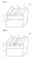
- Fig. 9 is a view representing the high electron mobility transistor according to other modification of Embodiment Mode 1.
- the high electron mobility transistor 11b can be provided with an AlGaN layer 15a, in place of the AlGaN layer 15 of the high electron mobility transistor 11a.
- the AlGaN layer 15a includes a first portion 15b, a second portion 15c, and a third portion 15d.
- the first portion 15b is positioned between the second portion 15c and the third portion 15d.
- the thickness of the first portion 15b is smaller than that of the second portion 15c and that of the third portion 15d, thereby forming a recess structure in the AlGaN layer 15a.
- a gate electrode 19a is provided on the first portion 15b.
- the recess structure is formed by thinning the Al y Ga 1- y N epitaxial layer 15 by etching, for example.
- the recess gate structure makes it possible to reduce the source resistance, improve the mutual conductance, and perform the normally off.
- Fig. 10 is a view representing the high electron mobility transistor according to other modification of Embodiment Mode 1.
- the high electron mobility transistor 11c may be provided with an AlGaN layer 15e, in place of the AlGaN layer 15 of the high electron mobility transistor 11a.
- the AlGaN layer 15e includes a first portion 15f, a second portion 15g, and a third portion 15h.
- the first portion 15f is positioned between the second portion 15g and the third portion 15h.
- the thickness of the first portion 15f is larger than that of the second portion 15g and that of the third portion 15h, thereby forming a recess structure in the AlGaN layer 15e.
- the recess structure can be formed by thinning the Al y Ga 1- y N epitaxial layer 15 by etching, for example.
- the source electrode 21a is provided on the second portion 15g, and the source electrode 23a is provided on the third portion 15h. This recess ohmic structure can reduce the contact resistance.
- Fig. 11 is a view representing the high electron mobility transistor according to other modification of Embodiment Mode 1.
- the high electron mobility transistor 11d can be furtherer provided with contact layers 16 for a source electrode and a drain electrode.
- the contact layers 16 are provided on the AlGaN layer 15 of the high electron mobility transistor 11a.
- the contact layers 16 may be composed of gallium nitride semiconductors such as GaN, InN, and InGaN.
- the band gap of the contact layer 16 is preferably smaller than that of the AlGaN layer 15.
- the carrier concentration of the contact layer 16 is preferably larger than that of the AlGaN layer 15.
- the gate electrode 19 constitutes a Schottky junction with the AlGaN layer 15, and the source electrode 21b and the drain electrode 23b constitute ohmic contacts with the contact layer.
- the contact layer added structure can reduce the contact resistance.
Landscapes
- Junction Field-Effect Transistors (AREA)
- Insulated Gate Type Field-Effect Transistor (AREA)
Abstract
Description
- The present invention relates to Group III nitride semiconductor devices and epitaxial substrates.
- In Non-Patent Document 1, high electron mobility transistors (HEMT) are disclosed. The high electron mobility transistors have an AlGaN/GaN heterostructure epitaxially grown on a sapphire substrate. In order to manufacture the high electron mobility transistors, after forming a low-temperature GaN layer on the sapphire substrate, an i-type GaN layer of 2 to 3 µm is formed. On the GaN layer, an i-type AlGaN layer of 7 nm, an n-type AlGaN layer of 15 nm, and an i-type AlGaN layer of 3 nm are formed in that order. The Schottky electrode is composed of Ni(3 nm)/Pt(300 nm)/Au(300 nm). Non-Patent Document 1: "Improvement of DC Characteristics of AlGaN/GaN High Electron Mobility Transistors Thermally Annealed Ni/Pt/Au Schottky Gate" Japanese Journal of Applied Physics Vol. 43, No. 4B, 2004, pp.1925-1929.
- High electron mobility transistors manufactured by conventional technology are provided with a GaN layer and an AlGaN layer on a supporting body of sapphire. A Schottky gate is formed on the episurface of the AlGaN layer. According to investigations by the inventors, in high electron mobility transistors manufactured using an epitaxial substrate provided with a GaN film and an AlGaN film on a sapphire substrate, the withstand voltage between the gate and the drain is low, such that the enhanced output power that is the goal is not attained. The reason for this is thought to be due to the larger leakage current from the gate electrode. In addition, according to experiments by the inventors, numerous screw dislocations are present in the AlGaN film. If the gate electrode is fabricated on the surface of the AlGaN film the Schottky barrier is lowered due to the interface state originating in the screw dislocations. As a result, the leakage current from the gate electrode becomes large.
- Although it is necessary to improve the crystal quality of the AlGaN film in order to lower the interface state, it is not easy to improve the crystal quality as expected. The inventors have conducted various experiments in order to investigate which kind of crystal quality of the AlGaN film is related to the leakage current from the gate electrode.
- An object of the present invention, brought about taking the above-described circumstances into consideration, is to make available Group III nitride semiconductor devices in which the leakage current from the Schottky electrode can be reduced, and meanwhile an object is to make available epitaxial substrates for manufacturing the Group III nitride semiconductor devices.
- One aspect of the present invention involves a Group III nitride semiconductor device. The Group III nitride semiconductor device is furnished with (a) a supporting substrate composed of Al x Ga1-x N (0 ≤ x ≤1), (b) an Al y Ga1-y N epitaxial layer (0 < y≤1) having a full-width-at-half maximum for (0002) plane XRD of 150 sec or less, (c) a GaN epitaxial layer provided between the supporting substrate and the Al y Ga1-y N epitaxial layer, (d) a Schottky electrode provided on the Al y Ga1-y N epitaxial layer, (e) a source electrode provided on the gallium nitride epitaxial layer, and (f) a drain electrode provided on the gallium nitride epitaxial layer.
- According to the experiments by the inventors, it has been found that the leakage current from the Schottky electrode in contact with the Al y Ga1-y N epitaxial layer (0 <y≤1) is related to the full-width-at-half maximum for (0002) plane XRD. According to the present invention, since the full-width-at-half maximum for (0002) plane XRD is 150 sec or less, the leakage current from the Schottky electrode can be reduced.
- In a Group III nitride semiconductor device involving the present invention, it is preferable that aluminum mole fraction y of the Al y Ga1-y N epitaxial layer be between 0.1 and 0.7, inclusive.
- If the aluminum mole fraction y is less than 0.1, the band offset becomes small so that two-dimensional electron gas having enough density at the AlGaN/GaN interface is not formed. If the aluminum mole fraction y is more than 0.7, it is highly likely that cracks are generated in the AlGaN layer. The generation of the cracks prevents the two-dimensional electron gas from being formed at the AlGaN/GaN interface.
- In a Group III nitride semiconductor device involving the present invention, it is preferable that the Al y Ga1-y N epitaxial layer has a thickness between 5 nm and 50 nm, inclusive.
- If the thickness of the Al y Ga1-y N epitaxial layer is less than 5 nm, the distortion at the AlGaN/GaN interface becomes small so that the two-dimensional electron gas can not be formed. If the thickness of the Al y Ga1-y N epitaxial layer is more than 50 nm, it is highly likely that the cracks are generated in the AlGaN layer. The generation of the cracks prevents the two-dimensional electron gas from being formed at the AlGaN/GaN interface.
- In a Group III nitride semiconductor device involving the present invention, it is preferable that the supporting substrate be composed of gallium nitride. As a result, a Group III nitride semiconductor device can be provided using a supporting substrate having a low dislocation density.
- A separate aspect of the present invention involves an epitaxial substrate for a Group III nitride semiconductor device. The epitaxial substrate is furnished with (a) a substrate composed of Al x Ga1-x N (0 ≤ x ≤1), (b) an Al y Ga1-y N epitaxial film (0 < y≤1) having a full width at half maximum for (0002) plane XRD of 150 sec or less, and (c) a gallium nitride epitaxial film provided between the substrate and the Al y Ga1-y N epitaxial film.
- According to the experiments by the inventors, it has been found that the leakage current from the Schottky electrode in contact with the Al y Ga1-y N epitaxial film (0 < y≤1) is related to the full width at half maximum for (0002) plane XRD. According to the epitaxial substrate, since the full width at half maximum for (0002) plane XRD is 150 sec or less, the leakage current from the Schottky electrode formed on the Al y Ga1-y N epitaxial film is small. Consequently, for example, epitaxial substrates preferably for high electron mobility transistors can be provided.
- In an epitaxial substrate involving the present invention, it is preferable that aluminum composition y of the Al y Ga1-y N epitaxial film be between 0.1 and 0.7, inclusive.
- If the aluminum mole fraction y of the Al y Ga1-y N epitaxial film is smaller than 0.1, the band offset becomes small so that two-dimensional electron gas having enough density at the AlGaN/GaN interface is not formed. If the aluminum mole fraction y of the Al y Ga1-y N epitaxial film is more than 0.7, it is highly likely that cracks are generated in the AlGaN layer. The generation of the cracks prevents the two-dimensional electron gas from being formed at the AlGaN/GaN interface.
- In an epitaxial substrate involving the present invention, it is preferable that the Al y Ga1-y N epitaxial film has a thickness between 5 nm and 50 nm, inclusive.
- If the thickness of the Al y Ga1-y N epitaxial layer is less than 5 nm, the distortion at the AlGaN/GaN interface becomes small so that the two-dimensional electron gas can not be formed. If the thickness of the Al y Ga1-y N epitaxial layer is more than 50 nm, it is highly likely that the cracks are generated in the AlGaN layer. The generation of the cracks prevents the two-dimensional electron gas from being formed at the AlGaN/GaN interface.
- In an epitaxial substrate involving the present invention, it is preferable that the substrate be a gallium nitride substrate. As a result, an epitaxial substrate can be provided for a Group III nitride semiconductor device using a substrate having a low dislocation density.
- From the following detailed description of the preferred embodiments of the present invention in conjunction with the accompanying drawings, the foregoing and other objects, features, aspects and advantages of the present invention will become readily apparent.
- As described above, the present invention affords a Group III nitride semiconductor device in which the leakage current from the Schottky electrode is decreased. Furthermore, the present invention affords an epitaxial substrate for manufacturing the Group III nitride semiconductor device.
-
- Fig. 1 is a view representing the high electron mobility transistor involving Embodiment Mode 1.
- Fig. 2A is a view representing the structure of the high electron mobility transistor (HEMT) in Embodiment Example.
- Fig. 2B is a view representing the structure of the HEMT in Experiment.
- Fig. 3 is a view representing a spectrum for (0002) plane XRD in the surfaces of the AlGaN layers of the epitaxial substrate (sample A) and the epitaxial substrate (sample B) manufactured for the high electron mobility transistors.
- Fig. 4 is a view representing correspondences between leakage current density and the full width at half maximum for (0002) plane XRD characteristic in the gallium nitride layer.
- Fig. 5A is a view representing the manufacture of the epitaxial substrate involving Embodiment Mode 2.
- Fig. 5B is a view representing the manufacture of the epitaxial substrate involving Embodiment Mode 2.
- Fig. 5C is a view representing the manufacture of the epitaxial substrate involving Embodiment Mode 2.
- Fig. 6 is a view representing one example of locations of the high dislocation regions and the low dislocation regions in the gallium nitride freestanding substrate for Embodiment Modes 1 and 2.
- Fig. 7 is a view representing another example of locations of the high dislocation areas and the low dislocation areas in the gallium nitride freestanding substrate for Embodiment Modes 1 and 2.
- Fig. 8 is a view representing the high electron mobility transistor according to one modification of Embodiment Mode 1.
- Fig. 9 is a view representing the high electron mobility transistor according to other modification of Embodiment Mode 1.
- Fig. 10 is a view representing the high electron mobility transistor according to other modification of Embodiment Mode 1.
- Fig. 11 is a view representing the high electron mobility transistor according to other modification of Embodiment Mode 1.
- 11, 11a, 11b, 11c, 11d: high electron mobility transistor; 13: supporting substrate; 14: additional gallium nitride semiconductor layer; 15: Al y Ga1-y N epitaxial layer (0<y≤1); 16: contact layer; 17: GaN epitaxial layer; 19, 19a: Schottky electrode; 21, 21a, 21b: source electrode; 23, 23a, 23b: drain electrode; 31: gallium nitride substrate; 33: gallium nitride film; 35: AlGaN film; A: epitaxial substrate; 37a: source electrode; 37b: drain electrode; 39: gate electrode; 41: sapphire substrate; 42: seed layer; 43: gallium nitride film; 45: AlGaN film; B: epitaxial substrate; 47a: source electrode; 47b: drain electrode; 49: gate electrode; 80: reactor; 83: gallium nitride freestanding substrate; 85: GaN epitaxial film; 87: AlGaN epitaxial film; 81: epitaxial substrate; 82: gallium nitride freestanding substrate; 82c: high dislocation region; 82d: low dislocation region; 84: gallium nitride supporting substrate; 84c: high dislocation region; 84d: low dislocation region.
- Insights into the present invention will be readily understood in conjunction with the following detailed description with reference to the accompanying figures for illustration. Hereinafter, referring to the accompanying figures, embodiments according to Group III nitride semiconductor devices and epitaxial substrates of the present invention will be described. In the embodiments, high electron mobility transistors as a Group III nitride semiconductor device will be described. Note that where possible identical components are labeled with the same reference marks.
- Fig. 1 is a view representing a high electron mobility transistor involving Embodiment Mode 1. The high
electron mobility transistor 11 is furnished with a supportingsubstrate 13, an Al y Ga1-y N epitaxial layer (0< y≤1) 15, aGaN epitaxial layer 17, aSchottky electrode 19, asource electrode 21, and adrain electrode 23. The supportingsubstrate 13 is composed of Al x Ga1-x N (0≤ x≤1), more specifically, AlN, AlGaN, or GaN. The Al y Ga1-yN epitaxial layer 15 has a full-width-at-half maximum for (0002) plane XRD of 150 sec or less. TheGaN epitaxial layer 17 is provided between the galliumnitride supporting substrate 13 and the Al y Ga1-yN epitaxial layer 15. TheSchottky electrode 19 is provided on the Al y Ga1-yN epitaxial layer 15. Thesource electrode 21 and thedrain electrode 23 are provided on theGaN epitaxial layer 17. As one example of the present embodiment, thesource electrode 21 may be provided on the Al y Ga1-yN epitaxial layer 15. Moreover, thedrain electrode 23 may be provided on the Al y Ga1-yN epitaxial layer 15. In this example, thesource electrode 21 is in contact with the Al y Ga1-yN epitaxial layer 15, and thedrain electrode 23 is in contact with the Al y Ga1-yN epitaxial layer 15. TheSchottky electrode 19 constitutes a gate electrode of the highelectron mobility transistor 11. - According to the inventors' experiments, it has been found that the leakage current from the
Schottky electrode 19 in contact with the Al y Ga1-yN epitaxial layer 15 is related to the full-width-at-half maximum for (0002) plane XRD. Since the full-width-at-half maximum for (0002) plane XRD is 150 sec or less, the leakage current from theSchottky electrode 19 can reduced. - Fig. 2A is a view representing structures of a high electron mobility transistor (HEMT) involving Embodiment Example. Fig. 2B is a view representing structures of an HEMT involving Experiment.
- A
gallium nitride substrate 31 is placed in a reactor of an MOVPE device. Supplying gases including hydrogen, nitrogen, and ammonia into the reactor, thegallium nitride substrate 31 undergoes a heat treatment at 1100 degrees Celsius for 20 minutes. Next, the temperature of thegallium nitride substrate 31 is increased to 1130 degrees Celsius. Ammonia and trimethylgallium (TMG) are supplied to the reactor to grow agallium nitride film 33 having a thickness of 1.5 µm on thegallium nitride substrate 31. Trimethyl aluminum (TMA), TMG, and ammonia are supplied into the reactor to grow anAlGaN film 35 of 30 nm on thegallium nitride film 33. By these processes, an epitaxial substrate A is manufactured. Asource electrode 37a and adrain electrode 37b of Ti/A1/Ti/Au are formed on a surface of the epitaxial substrate A, and agate electrode 39 of Au/Ni is formed on the surface of the epitaxial substrate A. By these processes, an HEMT-A shown in Fig. 2A is manufactured. - A
sapphire substrate 41 is placed in a reactor of the MOVPE device. Supplying the gases including hydrogen, nitrogen, and ammonia into the reactor, thesapphire substrate 41 undergoes a heat treatment at a temperature of 1170 degrees Celsius for 10 minutes. Next, aseed layer 42 is grown on thesapphire substrate 41. After this, as in Embodiment Example, agallium nitride film 43 and anAlGaN film 45 are grown to manufacture an epitaxial substrate B. Asource electrode 47a and adrain electrode 47b of Ti/Al/Ti/Au are formed on the surface of the epitaxial substrate B, and agate electrode 49 of Au/Ni is formed on the surface of the epitaxial substrate B. By these processes, an HEMT-B shown in Fig. 2B is manufactured. - Fig. 3 is a view representing a spectrum for (0002) plane XRD in the surfaces of the AlGaN layers of the epitaxial substrate (sample A) and the epitaxial substrate (sample B) manufactured for the high electron mobility transistors. The sample A includes a GaN film and an AlGaN film formed on the gallium nitride substrate in this order. The sample B includes a seed film, a GaN film and an AlGaN film formed on the sapphire substrate in this order. On each of the AlGaN films, a Schottky electrode is provided to measure the leakage current. The Schottky electrode has an area of 7.85×10⁻⁵ cm2, and the applied voltage is -5 volts, for example.
- Sample A -
FWHM of XRD: 22.4 (sec),
Leakage current density: 1.75×10⁻⁶ (A/cm2); - Sample B -
FWHM of XRD: 214.4 (sec),
Leakage current density: 1.79□ ×10-2 (A/cm2). - The leakage current in the sample A is largely reduced compared to the leakage current in the sample B. The reason is that as far as XRD of the AlGaN layer is concerned, FWHM of the sample A is more acute than that of the sample B.
- The XRD in the (0002) plane has a wider full-width-at-half maximum as the number of the screw dislocations included in the AlGaN layer is larger. Therefore, by making the full-width-at-half maximum small, the leakage current from the Schottky electrode can be reduced. The forward current through the gate electrode of the HEMT is about 0.1 A/cm-2, therefore, it is necessary to limit the leakage current to 1×10⁻⁴ A/cm2, 1/1000 of the forward current or less. As shown in Fig. 4, since the Al y Ga1-y N epitaxial layer has a full-width-at-half maximum for (0002) plane XRD of 150 sec or less, the leakage current can be 1×10⁻⁴ A/cm2 or less. Although it is principally possible to evaluate the crystal quality of the AlGaN layer with XRDs of (0004) plane or (0006) plane, other than (0002) plane, (0002) plane is preferable for evaluating the crystal quality of the AlGaN layer because (0002) plane has the great XRD strength.
- Fig. 4 is a view representing correspondences between leakage current density and the full-width-at-half maximum for (0002) plane XRD characteristic in the gallium nitride layer. Symbols indicated by
reference marks 51a through 51h represent values obtained by measuring structures in which Schottky electrodes are manufactured on the AlGaN layer fabricated by utilizing the gallium nitride substrate. Symbols indicated byreference marks 53a through 53f represent values obtained by measuring structures in which Schottky electrodes are formed on the AlGaN layers fabricated by utilizing the sapphire substrates. - To present specific examples:
- Sample indicated by the
reference mark 51a-Full-width-at-half maximum: 22.4 sec, - Leakage current density: 1.75×10⁻⁶ A/cm2;
- Sample indicated by the
reference mark 51b-Full-width-at-half maximum: 70.3 sec, - Leakage current density: 4.37×10⁻⁵ A/cm2;
- Sample indicated by the
reference mark 51c-Full-width-at-half maximum: 70.3 sec, - Leakage current density: 1.11×10⁻⁵ A/cm2;
- Sample indicated by the
reference mark 51d-Full-width-at-half maximum: 70.9 sec, - Leakage current density: 9.01×10⁻⁷ A/cm2;
- Sample indicated by the
reference mark 51e-Full-width-at-half maximum: 70.9 sec, - Leakage current density: 2.72× 10⁻⁸ A/cm2;
- Sample indicated by the
reference mark 51f-Full-width-at-half maximum: 110.1 sec, - Leakage current density: 2.45×10⁻⁶ A/cm2;
- Sample indicated by the
reference mark 51g-Full-width-at-half maximum: 124.8 sec, - Leakage current density: 3.05×10⁻⁵ A/cm2;
- Sample indicated by the
reference mark 51h-Full-width-at-half maximum: 141.3 sec, - Leakage current density: 9.70×10⁻⁶ A/cm2.
- To present a specific example:
- Schottky diode structure of the
reference mark 53a (with the smallest full-width-at-half maximum and leakage current density). - Full-width-at-half maximum: 182.6 sec,
- Leakage current density: 2.15×10⁻³ A/cm2.
- In the high
electron mobility transistor 11, a supportingsubstrate 13 of nitride is composed of gallium nitride conductive or semi-insulating. In this example, the gallium nitride region is homoepitaxially grown on the gallium nitride supporting substrate. The gallium nitride supporting substrate has a carrier concentration of 1×1019 cm-3 or less. TheGaN layer 17 has a thickness between 0.1 µm and 1000 µm, inclusive. TheGaN layer 17 has a carrier concentration of 1×1017 cm-3 or less. TheAlGaN layer 15 has a thickness between 5 nm and 50 nm, inclusive. TheAlGaN layer 15 has a carrier concentration of 1×1019 cm-3 or less. - In the high
electron mobility transistor 11, aluminum composition Y of the Al y Ga1-yN epitaxial layer 15 is preferably 0.1 or more. If the aluminum composition Y is less than 0.1, the band offset becomes small so that two-dimensional electron gas having enough density can not be formed at the AlGaN/GaN interface. Furthermore, the aluminum composition Y is preferably 0.7 or less. If the aluminum composition Y is more than 0.7, it is highly likely that cracks are generated in the AlGaN layer. The generation of the cracks prevents the two-dimensional electron gas from being formed at the AlGaN/GaN interface. - In the high
electron mobility transistor 11, the Al y Ga1-yN epitaxial layer 15 preferably has a thickness of 5 nm or more. If the thickness of the Al y Ga1-yN epitaxial layer 15 is less than 5 nm, the distortion at the AlGaN/GaN interface becomes small and the two-dimensional electron gas is not formed. Furthermore, the Al y Ga1-yN epitaxial layer 15 preferably has a thickness of 50 nm or less. If the thickness of the Al y Ga1-y N epitaxial layer is more than 50 nm, it is highly likely that the cracks are generated in the AlGaN layer. The generation of cracks prevents the two-dimensional electron gas from being formed at the AlGaN/GaN interface. - The Al x Ga1-x N supporting substrate for the high
electron mobility transistor 11 is preferably composed of gallium nitride. Accordingly, Group III nitride semiconductor devices are provided using a supporting substrate of a low dislocation density. - Fig. 5A, Fig. 5B, and Fig. 5C are views representing manufacture of the epitaxial substrate according to Embodiment Mode 2. As shown in Fig. 5A, a gallium nitride
freestanding substrate 83 having conductivity is placed in areactor 80. The following crystal growth is preferably performed by MOVPE method. The gallium nitridefreestanding substrate 83 has a carrier concentration of 1×1019 cm-3 or less. As shown in Fig. 5B, by supplying TMG and NH3, aGaN epitaxial film 85 is deposited on afirst surface 83a of the gallium nitridefreestanding substrate 83. TheGaN epitaxial film 85 is preferably undoped. TheGaN epitaxial film 85 is deposited at a temperature between 600 degrees Celsius and 1200 degrees Celsius, inclusive. The pressure in the reactor is between 1 kPa and 120 kPa, inclusive. The galliumnitride epitaxial film 85 has a thickness between 0.5 µm and 1000 µm, inclusive. TheGaN epitaxial film 85 has a carrier concentration of 1×1017 cm-3 or less. If necessary, in advance of the growth of theGaN epitaxial film 85, a buffer layer can be grown. The buffer layer may be composed of any of AIN, GaN, AlGaN, InGaN, and AlInGaN. The buffer layer restrains defects or impurities of the gallium nitridefreestanding substrate 83 from affecting theGaN epitaxial layer 85, so that quality of theGaN epitaxial layer 85 can be improved.
Next, as shown in Fig. 5C, TMA, TMG and NH3 are supplied to deposit an undoped or n-typeAlGaN epitaxial film 87 onto the undopedGaN epitaxial film 85. TheAlGaN epitaxial film 87 is deposited at a temperature between 600 degrees Celsius and 1200 degrees Celsius, inclusive. The pressure in the reactor is between 1 kPa and 120 kPa, inclusive. The aluminum composition of theAlGaN epitaxial film 87 is between 0.1 and 0.7, inclusive. TheAlGaN epitaxial film 87 has a thickness of 5 nm and 50 nm, inclusive. TheAlGaN epitaxial film 87 has a carrier concentration of 1×1019 cm-3 or less. Accordingly, anepitaxial substrate 81 is obtained. By making use of this substrate, an HEMT according to Embodiment Mode 1 can be manufactured. - The inventors have found that the leakage current from the Schottky electrode in contact with the Al y Ga1-y N epitaxial film 87 (0< y≤1) is related to the full-width-at-half maximum for (0002) plane XRD. In the epitaxial substrate, the leakage current from the Schottky electrode formed on the Al y Ga1-y N epitaxial is small. Accordingly, an epitaxial substrate preferable for the high electron mobility transistor can be provided, for example. Especially, if the full-width-at-half maximum for (0002) plane XRD is 150 sec or less, as apparent from Fig. 4, it is possible to reduce the leakage current from the Schottky electrode compared to a case of 150 sec or more.
- On a surface of the
AlGaN epitaxial film 87 of theepitaxial substrate 81, a Schottky electrode film for a gate electrode and ohmic electrode films for a source electrode and a drain electrode are deposited. The Schottky electrode and the ohmic electrode are formed from the Schottky electrode film and the ohmic electrode film, respectively. After thinning a portion of theAlGaN epitaxial film 87 immediately under the Schottky electrode, a Schottky electrode may be formed on the portion. Accordingly, it is possible to reduce the source resistance, improve the mutual conductance, and perform normally off. Furthermore, by adding n-type dopant, an n-type semiconductor region may be formed immediately under the source electrode and/or the drain electrode. Furthermore, n-type semiconductor regions to which n-type dopant is added may be grown as contact layers on the surface of theAlGaN epitaxial film 87, and on the contact layers a source electrode and/or a drain electrode may be formed. Accordingly, the contact resistance can be reduced. Furthermore, after thinning a portion of the AlGaN layer, a source and/or a drain electrode may be formed on the portion. Accordingly, the contact resistance can be reduced. Alternatively, the source and/or drain electrode may be formed to be in contact with the GaN layer having a band gap smaller than that of AlGaN by removing the AlGaN layer. Accordingly, the contact resistance can be reduced. Since the full-width-at-half maximum for (0002) plane XRD in the AlGaN region is used as an indicator of the crystal quality to monitor the quality of the AlGaN film with which the Schottky electrode constitutes a Schottky junction, an epitaxial substrate can be provided for semiconductor devices in which the backward leak current flowing through the Schottky junction when a voltage is applied across the Schottky electrode and the ohmic electrode can be reduced. - Fig. 6 is a view representing one example of locations of high dislocation regions and low dislocation regions in a gallium nitride freestanding substrate for Embodiment Modes 1 and 2. A
first surface 82a of the gallium nitridefreestanding substrate 82 for theepitaxial substrate 81 includes first areas wherehigh dislocation regions 82c having a relatively large screw dislocation density appear, and a second area where alow dislocation region 82d having a relatively small screw dislocation density appears. Thehigh dislocation regions 82c are surrounded by thelow dislocation region 82d, and the first areas are randomly distributed in a dot-like pattern in the second area on thefirst surface 82a. As a whole, the screw dislocation density is 1×108 cm-2 or less, for example. Theepitaxial substrate 81 gives an epitaxial layer having a lowered dislocation density in thelow dislocation region 82d. Consequently, the backward leak current is reduced and the backward breakdown voltage is improved. - Fig. 7 is a view representing another example of locations of the high dislocation regions and the low dislocation regions in a gallium nitride freestanding substrate for Embodiment Modes 1 and 2. A
first surface 84a of the gallium nitridefreestanding substrate 84 for theepitaxial substrate 81 includes first areas wherehigh dislocation regions 84c having a relatively large screw dislocation density appear, and second areas wherelow dislocation regions 84d having a relatively small screw dislocation density appear. Thehigh dislocation regions 84c are surrounded by thelow dislocation regions 84d, and the first areas are distributed in a striped pattern in the second area on thefirst surface 84a. As a whole, the screw dislocation density is 1×108 cm-2 or less, for example. Theepitaxial substrate 81 gives an epitaxial layer having a lowered dislocation density in thelow dislocation regions 84d. Accordingly, the backward leak current is decreased, and the backward breakdown voltage is improved. - In the present embodiment, as in Embodiment Mode 1, as a freestanding substrate, the Al x Ga1-x N (0≤ x≤ x≤1) substrate can be used. More specifically, the freestanding substrate can be composed ofAlN, AlGaN or GaN.
- Fig. 8 is a view representing the high electron mobility transistor according to one modification of Embodiment Mode 1. Referring to Fig. 8, the high
electron mobility transistor 11a can be provided with an additional galliumnitride semiconductor layer 14 between theGaN epitaxial layer 17 and the galliumnitride supporting substrate 13. The galliumnitride semiconductor layer 14 is composed of A1N, GaN, AlGaN, InGaN, or AlInGaN, for example. The galliumnitride semiconductor layer 14 restrains the affects of defects of and impurities on the supporting substrate from propagating to upper layers, thereby improving the quality of theGaN epitaxial layer 17. - Fig. 9 is a view representing the high electron mobility transistor according to other modification of Embodiment Mode 1. The high
electron mobility transistor 11b can be provided with anAlGaN layer 15a, in place of theAlGaN layer 15 of the highelectron mobility transistor 11a. TheAlGaN layer 15a includes afirst portion 15b, asecond portion 15c, and athird portion 15d. Thefirst portion 15b is positioned between thesecond portion 15c and thethird portion 15d. The thickness of thefirst portion 15b is smaller than that of thesecond portion 15c and that of thethird portion 15d, thereby forming a recess structure in theAlGaN layer 15a. On thefirst portion 15b, a gate electrode 19a is provided. The recess structure is formed by thinning the Al y Ga1-yN epitaxial layer 15 by etching, for example. The recess gate structure makes it possible to reduce the source resistance, improve the mutual conductance, and perform the normally off. - Fig. 10 is a view representing the high electron mobility transistor according to other modification of Embodiment Mode 1. The high
electron mobility transistor 11c may be provided with an AlGaN layer 15e, in place of theAlGaN layer 15 of the highelectron mobility transistor 11a. The AlGaN layer 15e includes afirst portion 15f, asecond portion 15g, and athird portion 15h. Thefirst portion 15f is positioned between thesecond portion 15g and thethird portion 15h. The thickness of thefirst portion 15f is larger than that of thesecond portion 15g and that of thethird portion 15h, thereby forming a recess structure in the AlGaN layer 15e. The recess structure can be formed by thinning the Al y Ga1-yN epitaxial layer 15 by etching, for example. Thesource electrode 21a is provided on thesecond portion 15g, and thesource electrode 23a is provided on thethird portion 15h. This recess ohmic structure can reduce the contact resistance. - Fig. 11 is a view representing the high electron mobility transistor according to other modification of Embodiment Mode 1. The high
electron mobility transistor 11d can be furtherer provided withcontact layers 16 for a source electrode and a drain electrode. The contact layers 16 are provided on theAlGaN layer 15 of the highelectron mobility transistor 11a. The contact layers 16 may be composed of gallium nitride semiconductors such as GaN, InN, and InGaN. The band gap of thecontact layer 16 is preferably smaller than that of theAlGaN layer 15. In addition, the carrier concentration of thecontact layer 16 is preferably larger than that of theAlGaN layer 15. Thegate electrode 19 constitutes a Schottky junction with theAlGaN layer 15, and thesource electrode 21b and thedrain electrode 23b constitute ohmic contacts with the contact layer. The contact layer added structure can reduce the contact resistance. - In the preferable embodiments, principles of the present invention were described with illustrations, but it will be recognized by persons skilled in the art that the present invention can be changed in locations and in detail without departing from the principles. The present invention is not limited to the specific configurations disclosed in the present embodiments. Accordingly, the rights in the scope of the patent claims, and in all modifications and changes deriving from the scope of the spirit thereof are claimed.
Claims (8)
- A Group III nitride semiconductor device characterized in being furnished with:a supporting substrate composed of Al x Ga1-x N (0≤x≤1);an Al y Ga1-y N epitaxial layer (0 < y ≤1) having a full-width-at-half maximum for (0002) plane XRD of 150 sec or less;a gallium nitride epitaxial layer provided between said supporting substrate and said Al y Ga1-y N epitaxial layer;a Schottky electrode provided on said Al y Ga1-y N epitaxial layer;a source electrode provided on said gallium nitride epitaxial layer; anda drain electrode provided on said gallium nitride epitaxial layer.
- The Group III nitride semiconductor device set forth in claim 1, characterized in that aluminum composition y of said Al y Ga1-y N epitaxial layer is between 0.1 and 0.7, inclusive.
- The Group III nitride semiconductor device set forth in claim 1 or 2, characterized in that said Al y Ga1-y N epitaxial layer has a thickness between 5 nm and 50 nm, inclusive.
- The Group III nitride semiconductor device set forth in any of claims 1 through 3, characterized in that said Al x Ga1-x N supporting substrate is composed of gallium nitride.
- An epitaxial substrate for a Group III nitride semiconductor device, said epitaxial substrate characterized in being furnished with:a substrate composed of Al x Ga1-x N (0≤x≤1);an Al y Ga1-y N epitaxial film (0<y≤1) having a full-width-at-half maximum for (0002) plane XRD of 150 sec or less; anda gallium nitride epitaxial film provided between said substrate and said Al y Ga1-y N epitaxial film.
- The epitaxial substrate set forth in claim 5, characterized in that aluminum composition yof said Al y Ga1-y N epitaxial film is between 0.1 and 0.7, inclusive.
- The epitaxial substrate set forth in claim 5 or 6, characterized in that said Al y Ga1-y N epitaxial film has a thickness between 5 nm and 50 nm, inclusive.
- The epitaxial substrate set forth in any of claims 5 through 7, characterized in that said Al x Ga1-x N substrate is a gallium nitride substrate.
Applications Claiming Priority (3)
| Application Number | Priority Date | Filing Date | Title |
|---|---|---|---|
| JP2005084378 | 2005-03-23 | ||
| JP2006019473A JP5135686B2 (en) | 2005-03-23 | 2006-01-27 | Group III nitride semiconductor device |
| PCT/JP2006/304262 WO2006100897A1 (en) | 2005-03-23 | 2006-03-06 | Group iii nitride semiconductor device and epitaxial substrate |
Publications (2)
| Publication Number | Publication Date |
|---|---|
| EP1863075A1 true EP1863075A1 (en) | 2007-12-05 |
| EP1863075A4 EP1863075A4 (en) | 2009-04-29 |
Family
ID=37023571
Family Applications (1)
| Application Number | Title | Priority Date | Filing Date |
|---|---|---|---|
| EP06715282A Ceased EP1863075A4 (en) | 2005-03-23 | 2006-03-06 | GROUP III NITRIDE SEMICONDUCTOR DEVICE AND EPITAXIAL SUBSTRATE |
Country Status (8)
| Country | Link |
|---|---|
| US (1) | US8410524B2 (en) |
| EP (1) | EP1863075A4 (en) |
| JP (1) | JP5135686B2 (en) |
| KR (1) | KR20070113094A (en) |
| CN (1) | CN1969380B (en) |
| CA (1) | CA2564424A1 (en) |
| TW (1) | TW200701459A (en) |
| WO (1) | WO2006100897A1 (en) |
Cited By (1)
| Publication number | Priority date | Publication date | Assignee | Title |
|---|---|---|---|---|
| WO2013120990A1 (en) * | 2012-02-17 | 2013-08-22 | Isos Technologies Sarl | Hemt heterostructure and a method of hemt manufacturing |
Families Citing this family (5)
| Publication number | Priority date | Publication date | Assignee | Title |
|---|---|---|---|---|
| EP2221855A4 (en) * | 2007-11-21 | 2013-08-07 | Mitsubishi Chem Corp | NITRIDE SEMICONDUCTOR AND METHOD FOR GROWING NITRIDE SEMICONDUCTOR CRYSTAL |
| JP5453780B2 (en) * | 2008-11-20 | 2014-03-26 | 三菱化学株式会社 | Nitride semiconductor |
| JP5564842B2 (en) | 2009-07-10 | 2014-08-06 | サンケン電気株式会社 | Semiconductor device |
| KR20120027988A (en) | 2010-09-14 | 2012-03-22 | 삼성엘이디 주식회사 | Gallium nitride based semiconductor device and method of manufacturing the same |
| KR101922117B1 (en) | 2012-08-16 | 2018-11-26 | 삼성전자주식회사 | Electronic device including transistor and method of operating the same |
Family Cites Families (11)
| Publication number | Priority date | Publication date | Assignee | Title |
|---|---|---|---|---|
| JP4033519B2 (en) * | 1997-06-27 | 2008-01-16 | シャープ株式会社 | Gallium nitride compound semiconductor light emitting device |
| US6372041B1 (en) * | 1999-01-08 | 2002-04-16 | Gan Semiconductor Inc. | Method and apparatus for single crystal gallium nitride (GaN) bulk synthesis |
| US6592663B1 (en) * | 1999-06-09 | 2003-07-15 | Ricoh Company Ltd. | Production of a GaN bulk crystal substrate and a semiconductor device formed on a GaN bulk crystal substrate |
| JP3836697B2 (en) * | 2000-12-07 | 2006-10-25 | 日本碍子株式会社 | Semiconductor element |
| JP2002289528A (en) * | 2001-03-23 | 2002-10-04 | Yasuhiko Arakawa | Crystal growth method of gallium nitride compound semiconductor and electronic device provided with gallium nitride compound semiconductor |
| JP4906023B2 (en) * | 2001-08-14 | 2012-03-28 | 古河電気工業株式会社 | GaN-based semiconductor device |
| JP2005530334A (en) * | 2002-04-30 | 2005-10-06 | クリー・インコーポレーテッド | High voltage switching element and process for forming the same |
| JP2004327882A (en) * | 2003-04-28 | 2004-11-18 | Ngk Insulators Ltd | Epitaxial substrate, semiconductor device, and high electron-mobility transistor |
| US20070184671A1 (en) | 2003-05-30 | 2007-08-09 | Showa Denko K.K. | Method for production of group lll nitride semiconductor device |
| JP2005244207A (en) * | 2004-01-30 | 2005-09-08 | Showa Denko Kk | Gallium nitride compound semiconductor light emitting device |
| US7687827B2 (en) * | 2004-07-07 | 2010-03-30 | Nitronex Corporation | III-nitride materials including low dislocation densities and methods associated with the same |
-
2006
- 2006-01-27 JP JP2006019473A patent/JP5135686B2/en not_active Expired - Fee Related
- 2006-03-06 WO PCT/JP2006/304262 patent/WO2006100897A1/en not_active Ceased
- 2006-03-06 CA CA002564424A patent/CA2564424A1/en not_active Abandoned
- 2006-03-06 KR KR1020067024397A patent/KR20070113094A/en not_active Withdrawn
- 2006-03-06 EP EP06715282A patent/EP1863075A4/en not_active Ceased
- 2006-03-06 CN CN200680000315XA patent/CN1969380B/en not_active Expired - Fee Related
- 2006-03-06 US US11/569,500 patent/US8410524B2/en not_active Expired - Fee Related
- 2006-03-13 TW TW095108455A patent/TW200701459A/en unknown
Cited By (1)
| Publication number | Priority date | Publication date | Assignee | Title |
|---|---|---|---|---|
| WO2013120990A1 (en) * | 2012-02-17 | 2013-08-22 | Isos Technologies Sarl | Hemt heterostructure and a method of hemt manufacturing |
Also Published As
| Publication number | Publication date |
|---|---|
| TW200701459A (en) | 2007-01-01 |
| CN1969380B (en) | 2012-08-22 |
| JP2006303439A (en) | 2006-11-02 |
| US8410524B2 (en) | 2013-04-02 |
| EP1863075A4 (en) | 2009-04-29 |
| JP5135686B2 (en) | 2013-02-06 |
| CN1969380A (en) | 2007-05-23 |
| KR20070113094A (en) | 2007-11-28 |
| CA2564424A1 (en) | 2006-09-28 |
| WO2006100897A1 (en) | 2006-09-28 |
| US20090189186A1 (en) | 2009-07-30 |
Similar Documents
| Publication | Publication Date | Title |
|---|---|---|
| CN101842884B (en) | Group III nitride electronic devices and Group III nitride semiconductor epitaxial substrates | |
| US8653561B2 (en) | III-nitride semiconductor electronic device, and method of fabricating III-nitride semiconductor electronic device | |
| KR101272365B1 (en) | Semiconductor device and fabrication method | |
| JP5465469B2 (en) | Epitaxial substrate, semiconductor device substrate, and HEMT element | |
| JP3960957B2 (en) | Semiconductor electronic device | |
| US8987015B2 (en) | Method for fabricating semiconductor device | |
| US20080265258A1 (en) | Group III Nitride Semiconductor Device and Epitaxial Substrate | |
| EP2290696B1 (en) | Epitaxial substrate for semiconductor device, semiconductor device, and method of manufacturing epitaxial substrate for semiconductor device | |
| US20120211801A1 (en) | Group iii nitride laminated semiconductor wafer and group iii nitride semiconductor device | |
| EP2251464B1 (en) | Epitaxial substrate for semiconductor device, semiconductor device, and method of manufacturing epitaxial substrate for semiconductor device | |
| JP2012015304A (en) | Semiconductor device | |
| US9401402B2 (en) | Nitride semiconductor device and nitride semiconductor substrate | |
| EP1876649A1 (en) | Group iii nitride semiconductor device and epitaxial substrate | |
| US20060081877A1 (en) | Semiconductor epitaxial wafer and field effect rtansistor | |
| US10777654B2 (en) | Method for manufacturing nitrogen-face polarity gallium nitride epitaxial structure | |
| US8410524B2 (en) | Group III nitride semiconductor device and epitaxial substrate | |
| US7554132B2 (en) | Electronic device containing group-III element based nitride semiconductors | |
| JP2010045416A (en) | Group iii nitride electronic device | |
| Matsuoka et al. | N-Polar growth of nitride semiconductors with MOVPE and its applications | |
| JP4972879B2 (en) | Field effect transistor, semiconductor device, and epitaxial substrate | |
| JP2006196557A (en) | Semiconductor epitaxial wafer and field effect transistor | |
| CN1977367A (en) | Group III nitride semiconductor device and epitaxial substrate |
Legal Events
| Date | Code | Title | Description |
|---|---|---|---|
| PUAI | Public reference made under article 153(3) epc to a published international application that has entered the european phase |
Free format text: ORIGINAL CODE: 0009012 |
|
| 17P | Request for examination filed |
Effective date: 20061115 |
|
| AK | Designated contracting states |
Kind code of ref document: A1 Designated state(s): DE FR GB NL |
|
| DAX | Request for extension of the european patent (deleted) | ||
| RBV | Designated contracting states (corrected) |
Designated state(s): DE FR GB NL |
|
| A4 | Supplementary search report drawn up and despatched |
Effective date: 20090326 |
|
| RIC1 | Information provided on ipc code assigned before grant |
Ipc: H01L 21/20 20060101ALN20090320BHEP Ipc: H01L 29/20 20060101ALN20090320BHEP Ipc: H01L 29/778 20060101AFI20090320BHEP |
|
| 17Q | First examination report despatched |
Effective date: 20090526 |
|
| REG | Reference to a national code |
Ref country code: DE Ref legal event code: R003 |
|
| STAA | Information on the status of an ep patent application or granted ep patent |
Free format text: STATUS: THE APPLICATION HAS BEEN REFUSED |
|
| 18R | Application refused |
Effective date: 20140801 |