EP1860922A1 - Method and apparatus to power light emitting diode arrays - Google Patents
Method and apparatus to power light emitting diode arrays Download PDFInfo
- Publication number
- EP1860922A1 EP1860922A1 EP07250124A EP07250124A EP1860922A1 EP 1860922 A1 EP1860922 A1 EP 1860922A1 EP 07250124 A EP07250124 A EP 07250124A EP 07250124 A EP07250124 A EP 07250124A EP 1860922 A1 EP1860922 A1 EP 1860922A1
- Authority
- EP
- European Patent Office
- Prior art keywords
- coupled
- circuit
- power supply
- load
- voltage
- Prior art date
- Legal status (The legal status is an assumption and is not a legal conclusion. Google has not performed a legal analysis and makes no representation as to the accuracy of the status listed.)
- Granted
Links
- 238000000034 method Methods 0.000 title abstract description 5
- 238000003491 array Methods 0.000 title description 3
- 230000001419 dependent effect Effects 0.000 claims 2
- 238000010586 diagram Methods 0.000 description 8
- 239000003990 capacitor Substances 0.000 description 5
- 238000001228 spectrum Methods 0.000 description 4
- 238000002156 mixing Methods 0.000 description 2
- 230000001105 regulatory effect Effects 0.000 description 2
- 230000005669 field effect Effects 0.000 description 1
- 230000010354 integration Effects 0.000 description 1
- 239000004973 liquid crystal related substance Substances 0.000 description 1
- 229910044991 metal oxide Inorganic materials 0.000 description 1
- 150000004706 metal oxides Chemical class 0.000 description 1
- 238000012986 modification Methods 0.000 description 1
- 230000004048 modification Effects 0.000 description 1
- 230000003287 optical effect Effects 0.000 description 1
- 239000004065 semiconductor Substances 0.000 description 1
- 239000002699 waste material Substances 0.000 description 1
- 238000004804 winding Methods 0.000 description 1
Images


Classifications
-
- H—ELECTRICITY
- H05—ELECTRIC TECHNIQUES NOT OTHERWISE PROVIDED FOR
- H05B—ELECTRIC HEATING; ELECTRIC LIGHT SOURCES NOT OTHERWISE PROVIDED FOR; CIRCUIT ARRANGEMENTS FOR ELECTRIC LIGHT SOURCES, IN GENERAL
- H05B45/00—Circuit arrangements for operating light-emitting diodes [LED]
- H05B45/40—Details of LED load circuits
- H05B45/44—Details of LED load circuits with an active control inside an LED matrix
- H05B45/46—Details of LED load circuits with an active control inside an LED matrix having LEDs disposed in parallel lines
-
- H—ELECTRICITY
- H05—ELECTRIC TECHNIQUES NOT OTHERWISE PROVIDED FOR
- H05B—ELECTRIC HEATING; ELECTRIC LIGHT SOURCES NOT OTHERWISE PROVIDED FOR; CIRCUIT ARRANGEMENTS FOR ELECTRIC LIGHT SOURCES, IN GENERAL
- H05B45/00—Circuit arrangements for operating light-emitting diodes [LED]
- H05B45/30—Driver circuits
- H05B45/37—Converter circuits
- H05B45/3725—Switched mode power supply [SMPS]
- H05B45/38—Switched mode power supply [SMPS] using boost topology
-
- H—ELECTRICITY
- H05—ELECTRIC TECHNIQUES NOT OTHERWISE PROVIDED FOR
- H05B—ELECTRIC HEATING; ELECTRIC LIGHT SOURCES NOT OTHERWISE PROVIDED FOR; CIRCUIT ARRANGEMENTS FOR ELECTRIC LIGHT SOURCES, IN GENERAL
- H05B45/00—Circuit arrangements for operating light-emitting diodes [LED]
- H05B45/30—Driver circuits
- H05B45/37—Converter circuits
- H05B45/3725—Switched mode power supply [SMPS]
- H05B45/385—Switched mode power supply [SMPS] using flyback topology
-
- H—ELECTRICITY
- H05—ELECTRIC TECHNIQUES NOT OTHERWISE PROVIDED FOR
- H05B—ELECTRIC HEATING; ELECTRIC LIGHT SOURCES NOT OTHERWISE PROVIDED FOR; CIRCUIT ARRANGEMENTS FOR ELECTRIC LIGHT SOURCES, IN GENERAL
- H05B45/00—Circuit arrangements for operating light-emitting diodes [LED]
- H05B45/30—Driver circuits
- H05B45/37—Converter circuits
- H05B45/3725—Switched mode power supply [SMPS]
Definitions
- the present invention relates generally to power supplies, and more specifically, the present invention relates to powering electronic circuits.
- LED arrays are used for a variety of purposes. For example, such arrays are often applied in backlighting for liquid crystal displays (LCDs). Generation of white light for such displays is usually accomplished by mixing the light from red, green, and blue LEDs. For larger lighting applications, power is supplied to a large array of red, green, and blue LEDs, often from a single power supply.
- LCDs liquid crystal displays
- FIG. 1A is a block diagram illustrating generally an example schematic of a circuit providing power to an array of LEDs in accordance with the teachings of the present invention.
- FIG. 1B is a block diagram illustrating generally another example schematic of a circuit providing power to an array of LEDs in accordance with the teachings of the present invention.
- FIG. 2 is a schematic diagram illustrating generally an example of a load including a current source and a voltage limited component in accordance with the teachings of the present invention.
- FIG. 3 is a schematic diagram illustrating generally another example of a load including a current source and a voltage limited component in accordance with the teachings of the present invention.
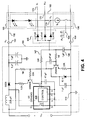
- FIG. 4 is a block diagram illustrating generally another example schematic of a circuit providing power to an array of LEDs in accordance with the teachings of the present invention.
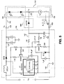
- FIG. 5 is a block diagram illustrating generally an example schematic of a circuit providing power to a string of LEDs in accordance with the teachings of the present invention.
- the spectrum of light from an LED is strongly influenced by the current in the LED.
- the LED When the LED is illuminated, it operates at a specified current to provide the desired optical spectrum.
- the average output from the LED is controlled by pulse width modulation (PWM) of the current in the LED.
- PWM pulse width modulation
- the LED conducts either the specified current or zero current at a duty ratio according to the PWM to achieve the desired output. Blending the spectra from red, green, and blue LEDs in the proper portions creates the desired white color and intensity of the backlight.
- each LED may typically operate at a different voltage that changes with operating temperature. These multiple LEDs may be of different color, such as for example red, green, and blue LEDs. Also, the desired spectrum from each color LED is obtained typically at a different operating current.
- the power supply should provide a voltage just high enough to illuminate all the LEDs at their rated current, since a higher voltage will waste power.
- various examples in accordance with the teachings of the present invention automatically adjust the voltage of a single power supply to provide sufficient voltage for an array of LEDs operating at different voltages and different currents at optimal efficiency.
- a single power supply that includes a feedback selector is used to obtain a single feedback signal from one of a plurality of current sources.
- each current source is included in a load that contains a voltage-limited component in accordance with the teachings of the present invention.
- the voltage-limited component comprises one or more LEDs.
- the feedback selector chooses the feedback signal to maintain the minimum voltage from the power supply to operate the LEDs in accordance with the teachings of the present invention.
- FIG. 1A shows generally one example of a circuit providing power to an array of LEDs in accordance with the teachings of the present invention.
- a backlighting circuit 100 includes a switching power supply circuit 105 coupled to one or more loads 160 and a feedback selector 165.
- Switching power supply circuit 105 receives an input voltage V IN at input terminals 135 and produces an output voltage Vo at terminals 150. In the illustrated example, all voltages are measured with respect to a common input and output return 148.
- switching power supply circuit 105 is a boost converter including an inductor 110 employed as an energy transfer element, an output rectifier 115, an output capacitor 120, and a switch 125.
- power supply circuit 105 is illustrated in FIG. 1A with a boost converter topology for explanation-purposes;-it-is appreciated that other power supply topologies may implemented in accordance with the teachings of the present invention.
- FIG. 1B shows generally a switching power supply circuit 105 having a flyback converter topology in accordance with the teachings of the present invention.
- a transformer having multiple windings is used as an energy transfer element instead of the inductor used in FIG. 1A.
- FIG. 1B All other aspects of the circuit illustrated generally in FIG. 1B are similar to the circuit illustrated in FIG. 1A. It is noted that still more example power supply topologies other than the example boost converter and flyback examples shown in FIG. 1A and FIG. 1B may be employed in the alternative, including for example a buck converter, or another suitable power supply topology in accordance with the teachings or the present invention.
- a switch 125 is switched on and off by a controller 140, which receives a feedback signal 145 from the feedback selector 165.
- feedback signal 145 is one of one or more N feedback signals 170 that are N voltages V 1 through V N corresponding to voltages across current sources I 1 185 through I N 190 or the one or more loads 160 in accordance with the teachings of the present invention.
- each of the one or more loads 160 includes a voltage-limited component 155, which in one example could be one or more LEDs that have different voltages.
- a voltage-limited component 155 which in one example could be one or more LEDs that have different voltages.
- rectifier diodes, Zener diodes, avalanche diodes, LEDs, batteries, or the like are examples of voltage-limited devices in accordance with the teachings of the present invention.
- the voltage across the voltage-limited component 155 does not increase substantially when the current through the component is greater than a conduction current.
- all of the one or more loads 160 receive the same voltage output voltage Vo 152 from the output terminals 150 of the power supply circuit 105.
- voltage V 1 is a switching voltage across current source 185 and voltage V N is a switching voltage across current source 190 of the one or more loads 160.
- Current source 185 conducts either current I 1 or zero current in response to the pulse width modulated signal Pi at terminal 175.
- Current source 190 conducts either current I N or zero current in response to pulse width modulated signal P N at terminal 180.
- the pulse width modulated signals P 1 ... P N are externally generated to control the current through each of the one or more loads 160. Therefore, each of the one or more loads 160 comprises a switch coupled to switch load current flowing in the respective load in response to the pulse width modulated signal in accordance with the teachings of the present invention.
- the pulse width modulated signals P 1 ... P N are generated externally, each of the current sources in the one or more loads 160 are switched "independently of the switching power supply 105 in accordance with the teachings of the present invention.
- Feedback selector 165 in the example of FIG. 1A causes the feedback voltage 145 to be the lowest of the continuum of switching voltages V 1 through V N of all of the one more loads 160.
- controller 140 then causes switching regulator 105 to produce an output voltage V 0 152 that maintains the feedback voltage 145 at a regulated voltage.
- feedback selector 165 is coupled to combine the continuum of feedback signals 170 received from all of the one or more loads 160 through a one or more respective diodes coupled to select one single feedback voltage 145 received at a single feedback terminal of the power supply circuit 105 in accordance with the teachings of the present invention.
- the power supply circuit 105 is coupled to be responsive to only one of the feedback signals 170 at any one time in accordance with the teachings of the present invention.
- the power supply 105 is responsive to only the lowest of the continuum of switching voltages received from feedback signal 170 in accordance with the teachings of the present invention.
- one or more loads 160 and one or more respective diodes in selector circuit 165 are included.
- a single load 160 having a single switched current source 190 and single voltage-limited component 155 may be included in accordance with the teachings of the present invention.
- only a single load 160 of multiple LEDs is powered by power supply 105 rather than a plurality of loads 160 or strings of LEDs.
- a single load 160 with a single feedback signal 170 from the switched current source 190 is included in accordance with the teachings of the present invention.
- Selector circuit 165 receives the single feedback signal 170 and selects the lowest of the continuum of switching voltages received from the single feedback signal 170 for feedback voltage 145 in accordance with the teachings of the present invention.
- the single load 160 has a switched current source 190 and a voltage-limited component 155 and is used with feedback selector circuit 165 having a single diode coupled between a single feedback terminal of the power supply circuit 105 and single load 160.
- the feedback selector circuit 165 receives the single feedback signal 170 from the switched current source 190, selects the lowest value of the single feedback signal 170 voltage from the continuum of switching voltages on the switched current source 190 as it is switched, and provides this lowest value of the single feedback signal 170 as the single feedback voltage 145 to which the power supply 105 is responsive in accordance with the teachings of the present invention.
- the current sources 185 through 190 of the loads 160 receive the difference between the output voltage V o 152 and the voltage across the voltage-limited components 155.
- the voltage-limited components 155 typically have a different voltage in each of the one or more loads 160.
- Each of the one or more loads 160 is coupled to conduct a load current specific to that load.
- the regulated feedback voltage 145 is chosen by a designer to be the minimum voltage to help ensure proper operation of the current sources 185 through 190 in the loads 160.
- FIG. 2 shows generally one example of a load 160 that includes a current source 190 and a voltage-limited component 155 in accordance with the teachings of the present invention.
- the illustrated voltage-limited component 155 includes a string of LEDs 210 coupled together.
- a transistor 215 is coupled to a shunt regulator 220 and a current sensing resistor 225 in the configuration of a constant current sink to regulate the current in the string of LEDs 210.
- the shunt regulator 220 is an LMV431 shunt regulator.
- resistor 205 provides the current necessary for the operation of transistor 215 and the shunt regulator 220.
- Transistor 230 with resistors 235 and 240 form a switch responsive to a pulse width modulated signal P N at a terminal 180.
- pulse width modulated signal P N is at a high level
- transistor 230 switches on to remove base current from transistor 215, and the current in the string of LEDs 210 is reduced to zero in accordance with the teachings of the present invention.
- the desired current is established in the string of LEDs 210 when approximately 1.24 volts are across the current sense resistor 225.
- transistor 215 functions as a current source when there is more than approximately 100 millivolts between the collector and emitter of transistor 215. Therefore, the example switching regulator 105 of the circuit of FIG. 1A would be designed to regulate the feedback voltage V N to a minimum value that is approximately 1.35 volts in the illustrated example.
- FIG. 3 shows generally another example of a load 160 that includes a current source 190 and a voltage-limited component 155 in accordance with the teachings of the present invention.
- the voltage-limited component 155 includes parallel strings of LEDs 310 coupled together as shown in the illustrated example. In one example, when the number of LEDs in each parallel string is large, current from the current source 190 will divide among the strings nearly equally.
- Current source 190 in the example shown in FIG. 3 includes a metal oxide semiconductor field effect transistor (MOSFET) 315 as an alternative to the bipolar transistor 215 example illustrated in FIG. 2. As shown in the example of FIG. 3, MOSFET 315 is driven by NPN bipolar transistor 320 from a bias voltage 305.
- a diode 325 is coupled to the gate of MOSFET 315, which allows rapid discharge of the gate capacitance of MOSFET 315 when NPN transistor 230 switches on as shown in the illustrated example.
- MOSFET metal oxide semiconductor field effect transistor
- FIG. 4 is a block diagram illustrating generally another example schematic of a circuit providing power to an array of LEDs in accordance with the teachings of the present invention.
- FIG. 4 shows details of a power supply with a load 160 that could be included in the circuit examples of FIG. 2 or FIG. 3.
- integrated circuit U 1 405 is a DPA424G device from Power Integrations, Inc., San Jose, California.
- the integrated circuit U1 405 includes a power MOSFET and a controller that performs the functions of the switch 125 and the controller 140 in FIG. 1A in accordance with the teachings of the present invention.
- FIG. 4 shows details of a power supply with a load 160 that could be included in the circuit examples of FIG. 2 or FIG. 3.
- integrated circuit U 1 405 is a DPA424G device from Power Integrations, Inc., San Jose, California.
- the integrated circuit U1 405 includes a power MOSFET and a controller that performs the functions of the switch 125 and the controller 140 in FIG. 1A
- selector circuit 165 includes LL4148 fast switching diodes coupled to receive each one of the feedback signals 170 from each respective one of the one or more loads 160. As shown, the plurality of diodes in selector circuit 165 are coupled together to provide a single feedback signal 145, to which integrated circuit U1 405 is responsive to regulate the output voltage Vo 152.
- capacitor 146 is coupled to provide feedback voltage 145 and is effectively a valley detector.
- capacitor 146 holds the lowest voltage that comes from the feedback selector 165, whether it is the lowest voltage from one load or from many loads.
- capacitor 146 may be a discrete capacitor or may be integrated in an integrated circuit in accordance with the teachings of the present invention.
- FIG. 5 is a block diagram illustrating generally an example schematic of a circuit providing power to a string of LEDs in accordance with the teachings of the present invention.
- the example circuit illustrated in FIG. 5 is similar to the example circuit illustrated in FIG. 4 except that one load 560 is illustrated in FIG. 5 with one corresponding LL4148 diode in selector circuit 565 to select the lowest of the continuum of voltages V N 570 in accordance with the teachings of the present invention.
- the specific example illustrated in FIG. 4 illustrates a plurality of loads 160 with a corresponding plurality of LL4148 diodes in selector circuit 165. Operation of the circuit illustrated in FIG. 5 is similar to the circuit illustrated in FIG. 4 in accordance with the teachings of the present invention.
Landscapes
- Dc-Dc Converters (AREA)
- Circuit Arrangement For Electric Light Sources In General (AREA)
- Led Devices (AREA)
Abstract
Description
- The present invention relates generally to power supplies, and more specifically, the present invention relates to powering electronic circuits.
- Light emitting diode (LED) arrays are used for a variety of purposes. For example, such arrays are often applied in backlighting for liquid crystal displays (LCDs). Generation of white light for such displays is usually accomplished by mixing the light from red, green, and blue LEDs. For larger lighting applications, power is supplied to a large array of red, green, and blue LEDs, often from a single power supply.
- Non-limiting and non-exhaustive embodiments of the present invention are described with reference to the following figures, wherein like reference numerals refer to like parts throughout the various views unless otherwise specified.
- FIG. 1A is a block diagram illustrating generally an example schematic of a circuit providing power to an array of LEDs in accordance with the teachings of the present invention.
- FIG. 1B is a block diagram illustrating generally another example schematic of a circuit providing power to an array of LEDs in accordance with the teachings of the present invention.
- FIG. 2 is a schematic diagram illustrating generally an example of a load including a current source and a voltage limited component in accordance with the teachings of the present invention.
- FIG. 3 is a schematic diagram illustrating generally another example of a load including a current source and a voltage limited component in accordance with the teachings of the present invention.
- FIG. 4 is a block diagram illustrating generally another example schematic of a circuit providing power to an array of LEDs in accordance with the teachings of the present invention.
- FIG. 5 is a block diagram illustrating generally an example schematic of a circuit providing power to a string of LEDs in accordance with the teachings of the present invention.
- Examples of apparatuses and methods for powering LEDs are disclosed. In the following description, numerous specific details are set forth in order to provide a thorough understanding of the present invention. It will be apparent, however, to one having ordinary skill in the art that the specific detail need not be employed to practice the present invention. Well-known methods related to the implementation have not been described in detail in order to avoid obscuring the present invention.
- Reference throughout this specification to "one embodiment" or "an embodiment" means that a particular feature, structure or characteristic described in connection with the embodiment is included in at least one embodiment of the present invention. Thus, the appearances of the phrases "in one embodiment" or "in an embodiment" in various places throughout this specification are not necessarily all referring to the same embodiment. Furthermore, the particular features, structures or characteristics may be combined for example into any suitable combinations and/or sub-combinations in one or more embodiments.
- As will be discussed, the spectrum of light from an LED is strongly influenced by the current in the LED. When the LED is illuminated, it operates at a specified current to provide the desired optical spectrum. The average output from the LED is controlled by pulse width modulation (PWM) of the current in the LED. As such, the LED conducts either the specified current or zero current at a duty ratio according to the PWM to achieve the desired output. Blending the spectra from red, green, and blue LEDs in the proper portions creates the desired white color and intensity of the backlight.
- A complication in providing power from a single power supply to multiple LEDs is that each LED may typically operate at a different voltage that changes with operating temperature. These multiple LEDs may be of different color, such as for example red, green, and blue LEDs. Also, the desired spectrum from each color LED is obtained typically at a different operating current. The power supply should provide a voltage just high enough to illuminate all the LEDs at their rated current, since a higher voltage will waste power. As will be discussed, various examples in accordance with the teachings of the present invention automatically adjust the voltage of a single power supply to provide sufficient voltage for an array of LEDs operating at different voltages and different currents at optimal efficiency.
- In one example, a single power supply that includes a feedback selector is used to obtain a single feedback signal from one of a plurality of current sources. In one example, each current source is included in a load that contains a voltage-limited component in accordance with the teachings of the present invention. In one example, the voltage-limited component comprises one or more LEDs. The feedback selector chooses the feedback signal to maintain the minimum voltage from the power supply to operate the LEDs in accordance with the teachings of the present invention.
- To illustrate, FIG. 1A shows generally one example of a circuit providing power to an array of LEDs in accordance with the teachings of the present invention. As shown, a
backlighting circuit 100 includes a switchingpower supply circuit 105 coupled to one ormore loads 160 and afeedback selector 165. Switchingpower supply circuit 105 receives an input voltage VIN atinput terminals 135 and produces an output voltage Vo atterminals 150. In the illustrated example, all voltages are measured with respect to a common input andoutput return 148. - In the example illustrated in FIG. 1A, switching
power supply circuit 105 is a boost converter including aninductor 110 employed as an energy transfer element, anoutput rectifier 115, anoutput capacitor 120, and aswitch 125. Althoughpower supply circuit 105 is illustrated in FIG. 1A with a boost converter topology for explanation-purposes;-it-is appreciated that other power supply topologies may implemented in accordance with the teachings of the present invention. For instance, FIG. 1B shows generally a switchingpower supply circuit 105 having a flyback converter topology in accordance with the teachings of the present invention. In the flyback converter topology illustrated generally in FIG. 1B, a transformer having multiple windings is used as an energy transfer element instead of the inductor used in FIG. 1A. All other aspects of the circuit illustrated generally in FIG. 1B are similar to the circuit illustrated in FIG. 1A. It is noted that still more example power supply topologies other than the example boost converter and flyback examples shown in FIG. 1A and FIG. 1B may be employed in the alternative, including for example a buck converter, or another suitable power supply topology in accordance with the teachings or the present invention. - Returning the specific example illustrated in FIG. 1A, during operation, a
switch 125 is switched on and off by acontroller 140, which receives afeedback signal 145 from thefeedback selector 165. In the illustrated example,feedback signal 145 is one of one or moreN feedback signals 170 that are N voltages V1 through VN corresponding to voltages across current sources I1 185 through IN 190 or the one ormore loads 160 in accordance with the teachings of the present invention. - As shown in FIG. 1A, each of the one or
more loads 160 includes a voltage-limited component 155, which in one example could be one or more LEDs that have different voltages. In general, rectifier diodes, Zener diodes, avalanche diodes, LEDs, batteries, or the like, are examples of voltage-limited devices in accordance with the teachings of the present invention. In operation, the voltage across the voltage-limitedcomponent 155 does not increase substantially when the current through the component is greater than a conduction current. In the illustrated example, all of the one ormore loads 160 receive the same voltageoutput voltage Vo 152 from theoutput terminals 150 of thepower supply circuit 105. - As shown in the depicted example, voltage V1 is a switching voltage across
current source 185 and voltage VN is a switching voltage acrosscurrent source 190 of the one or more loads 160.Current source 185 conducts either current I1 or zero current in response to the pulse width modulated signal Pi atterminal 175.Current source 190 conducts either current IN or zero current in response to pulse width modulated signal PN atterminal 180. In one example, the pulse width modulated signals P1 ... PN are externally generated to control the current through each of the one or more loads 160. Therefore, each of the one ormore loads 160 comprises a switch coupled to switch load current flowing in the respective load in response to the pulse width modulated signal in accordance with the teachings of the present invention. In addition, since the pulse width modulated signals P1 ... PN are generated externally, each of the current sources in the one ormore loads 160 are switched "independently of the switchingpower supply 105 in accordance with the teachings of the present invention. -
Feedback selector 165 in the example of FIG. 1A causes thefeedback voltage 145 to be the lowest of the continuum of switching voltages V1 through VN of all of the one more loads 160. In operation,controller 140 then causes switchingregulator 105 to produce anoutput voltage V 0 152 that maintains thefeedback voltage 145 at a regulated voltage. In the illustrated example,feedback selector 165 is coupled to combine the continuum of feedback signals 170 received from all of the one ormore loads 160 through a one or more respective diodes coupled to select onesingle feedback voltage 145 received at a single feedback terminal of thepower supply circuit 105 in accordance with the teachings of the present invention. Therefore, in an example with more than oneload 160, thepower supply circuit 105 is coupled to be responsive to only one of the feedback signals 170 at any one time in accordance with the teachings of the present invention. In an example with only oneload 160, thepower supply 105 is responsive to only the lowest of the continuum of switching voltages received fromfeedback signal 170 in accordance with the teachings of the present invention. - In the example illustrated in FIG. 1A, one or
more loads 160 and one or more respective diodes inselector circuit 165 are included. In another example, asingle load 160 having a single switchedcurrent source 190 and single voltage-limitedcomponent 155 may be included in accordance with the teachings of the present invention. For instance, in one such example, only asingle load 160 of multiple LEDs is powered bypower supply 105 rather than a plurality ofloads 160 or strings of LEDs. Thus, asingle load 160 with asingle feedback signal 170 from the switchedcurrent source 190 is included in accordance with the teachings of the present invention.Selector circuit 165 receives thesingle feedback signal 170 and selects the lowest of the continuum of switching voltages received from thesingle feedback signal 170 forfeedback voltage 145 in accordance with the teachings of the present invention. - In one
single load 160 example, thesingle load 160 has a switchedcurrent source 190 and a voltage-limitedcomponent 155 and is used withfeedback selector circuit 165 having a single diode coupled between a single feedback terminal of thepower supply circuit 105 andsingle load 160. In operation, thefeedback selector circuit 165 receives thesingle feedback signal 170 from the switchedcurrent source 190, selects the lowest value of thesingle feedback signal 170 voltage from the continuum of switching voltages on the switchedcurrent source 190 as it is switched, and provides this lowest value of thesingle feedback signal 170 as thesingle feedback voltage 145 to which thepower supply 105 is responsive in accordance with the teachings of the present invention. - Current sources generally require a minimum voltage to operate. Referring back to the specific circuit example in FIG. 1A with one or
more loads 160, thecurrent sources 185 through 190 of theloads 160 receive the difference between theoutput voltage V o 152 and the voltage across the voltage-limitedcomponents 155. In one example, the voltage-limitedcomponents 155 typically have a different voltage in each of the one or more loads 160. Each of the one ormore loads 160 is coupled to conduct a load current specific to that load. Theregulated feedback voltage 145 is chosen by a designer to be the minimum voltage to help ensure proper operation of thecurrent sources 185 through 190 in theloads 160. Thus, the circuit example illustrated in FIG. 1A operates with the highest efficiency since the lowest of the voltages V1 through VN is selected byfeedback selector 165 forfeedback voltage 145, which therefore should result in the lowestoutput voltage V o 152 and thereby in the lowest necessary dissipation of power in the current sources in accordance with the teachings of the present invention. - FIG. 2 shows generally one example of a
load 160 that includes acurrent source 190 and a voltage-limitedcomponent 155 in accordance with the teachings of the present invention. The illustrated voltage-limitedcomponent 155 includes a string ofLEDs 210 coupled together. In FIG. 2, atransistor 215 is coupled to ashunt regulator 220 and acurrent sensing resistor 225 in the configuration of a constant current sink to regulate the current in the string ofLEDs 210. In one example, theshunt regulator 220 is an LMV431 shunt regulator. In operation,resistor 205 provides the current necessary for the operation oftransistor 215 and theshunt regulator 220.Transistor 230 withresistors transistor 230 switches on to remove base current fromtransistor 215, and the current in the string ofLEDs 210 is reduced to zero in accordance with the teachings of the present invention. - In one example, the desired current is established in the string of
LEDs 210 when approximately 1.24 volts are across thecurrent sense resistor 225. In the illustrated example,transistor 215 functions as a current source when there is more than approximately 100 millivolts between the collector and emitter oftransistor 215. Therefore, theexample switching regulator 105 of the circuit of FIG. 1A would be designed to regulate the feedback voltage VN to a minimum value that is approximately 1.35 volts in the illustrated example. - FIG. 3 shows generally another example of a
load 160 that includes acurrent source 190 and a voltage-limitedcomponent 155 in accordance with the teachings of the present invention. The voltage-limitedcomponent 155 includes parallel strings ofLEDs 310 coupled together as shown in the illustrated example. In one example, when the number of LEDs in each parallel string is large, current from thecurrent source 190 will divide among the strings nearly equally.Current source 190 in the example shown in FIG. 3 includes a metal oxide semiconductor field effect transistor (MOSFET) 315 as an alternative to thebipolar transistor 215 example illustrated in FIG. 2. As shown in the example of FIG. 3,MOSFET 315 is driven by NPNbipolar transistor 320 from abias voltage 305. Adiode 325 is coupled to the gate ofMOSFET 315, which allows rapid discharge of the gate capacitance ofMOSFET 315 whenNPN transistor 230 switches on as shown in the illustrated example. - FIG. 4 is a block diagram illustrating generally another example schematic of a circuit providing power to an array of LEDs in accordance with the teachings of the present invention. In the illustrated example, FIG. 4 shows details of a power supply with a
load 160 that could be included in the circuit examples of FIG. 2 or FIG. 3. In the specific example shown in FIG. 4, integratedcircuit U 1 405 is a DPA424G device from Power Integrations, Inc., San Jose, California. Theintegrated circuit U1 405 includes a power MOSFET and a controller that performs the functions of theswitch 125 and thecontroller 140 in FIG. 1A in accordance with the teachings of the present invention. In the specific example shown in FIG. 4,selector circuit 165 includes LL4148 fast switching diodes coupled to receive each one of the feedback signals 170 from each respective one of the one or more loads 160. As shown, the plurality of diodes inselector circuit 165 are coupled together to provide asingle feedback signal 145, to whichintegrated circuit U1 405 is responsive to regulate theoutput voltage Vo 152. - In the circuit illustrated in FIG. 4,
capacitor 146 is coupled to providefeedback voltage 145 and is effectively a valley detector. In the illustrated example,capacitor 146 holds the lowest voltage that comes from thefeedback selector 165, whether it is the lowest voltage from one load or from many loads. In various examples, it is noted thatcapacitor 146 may be a discrete capacitor or may be integrated in an integrated circuit in accordance with the teachings of the present invention. - FIG. 5 is a block diagram illustrating generally an example schematic of a circuit providing power to a string of LEDs in accordance with the teachings of the present invention. The example circuit illustrated in FIG. 5 is similar to the example circuit illustrated in FIG. 4 except that one
load 560 is illustrated in FIG. 5 with one corresponding LL4148 diode inselector circuit 565 to select the lowest of the continuum of voltages VN 570 in accordance with the teachings of the present invention. In contrast, the specific example illustrated in FIG. 4 illustrates a plurality ofloads 160 with a corresponding plurality of LL4148 diodes inselector circuit 165. Operation of the circuit illustrated in FIG. 5 is similar to the circuit illustrated in FIG. 4 in accordance with the teachings of the present invention. - In the foregoing detailed description, the method and apparatus of the present invention have been described with reference to a specific exemplary embodiment thereof. It will, however, be evident that various modifications and changes may be made thereto without departing from the broader spirit and scope of the present invention. The present specification and figures are accordingly to be regarded as illustrative rather than restrictive.
Claims (21)
- A circuit (100), comprising:a power supply circuit (105) having input terminals (135) and output terminals (150), wherein the input terminals are to be coupled to receive a supply voltage (VIN), wherein a plurality of loads (160) are to be coupled between the output terminals, wherein the power supply circuit is coupled to provide an output voltage (Vo) between the output terminals to be applied across each one of the plurality of loads coupled between the output terminals; anda feedback selector circuit (165) coupled between the power supply circuit and the plurality of loads, wherein the feedback selector circuit is coupled to receive a feedback signal (170) from each one of the plurality of loads, wherein the power supply circuit is coupled to be responsive to only one of the feedback signals at any one time.
- A circuit according to claim 1, wherein each one of the plurality of loads comprises voltage-limited components (155).
- A circuit according to claim 2, wherein the voltage limited components comprise light emitting diodes.
- A circuit according to any preceding claim, wherein the feedback selector circuit is coupled to combine the feedback signals received from the plurality of loads through a plurality of diodes coupled to a single feedback terminal of the power supply circuit.
- A circuit according to any preceding claim, wherein the power supply circuit is a boost converter.
- A circuit according to any preceding claim, wherein each of the plurality of loads is coupled to conduct a load current specific to that load.
- A circuit according to claim 6, wherein each of the plurality of loads comprises a switch coupled to switch load current flowing in the respective load.
- A circuit according to claim 7, wherein the switch is coupled to be switched independently of the power supply circuit.
- A circuit according to claim 7 or 8, wherein each of the plurality of loads comprises a current source coupled to the switch.
- A circuit according to any of claims 1 to 4 or any claim dependent thereon, wherein the power supply circuit is a flyback converter.
- A circuit (100), comprising:a power supply circuit (105) having input terminals (135) and output terminals (150) wherein the input terminals are to be coupled to receive a supply voltage (VIN), wherein a load (160) is to be coupled between the output terminals, wherein the power supply circuit is coupled to provide an output voltage (Vo) between the output terminals to be applied across the load coupled between the output terminals; anda feedback selector circuit (165) coupled between the power supply circuit and the load, wherein the feedback selector circuit is coupled to receive feedback signal (170) from the load and select a lowest value of the feedback signal from a continuum of values to provide a single feedback voltage to which the power supply circuit is responsive.
- A circuit according to claim 11, wherein the load comprises voltage-limited components (155).
- A circuit according to claim 12, wherein the voltage limited components comprise light emitting diodes.
- A circuit according to any of claims 11 to 13, wherein the feedback selector circuit is coupled to receive the continuum of values of values of feedback signal from the load through a diode coupled to a single feedback terminal (145) of the power supply circuit.
- A circuit according to any of claims 11 to 14, wherein the power supply circuit is a boost converter.
- A circuit according to any of claims 11 to 15, wherein the load is coupled to conduct a load current specific to that load.
- A circuit according to claim 16, wherein the load comprises a switch coupled to switch the load current flowing in the respective load.
- A circuit according to claim 17, wherein the switch is coupled to be switched independently from the power supply circuit.
- A circuit according to claim 17, wherein the load comprises a current source coupled to the switch.
- A circuit according to any of claims 11 to 14 or any claim dependent thereon, wherein the power supply circuit is a flyback converter.
- An LCD device comprising a circuit according to any preceding claim.
Applications Claiming Priority (1)
| Application Number | Priority Date | Filing Date | Title |
|---|---|---|---|
| US11/440,606 US20070273681A1 (en) | 2006-05-24 | 2006-05-24 | Method and apparatus to power light emitting diode arrays |
Publications (2)
| Publication Number | Publication Date |
|---|---|
| EP1860922A1 true EP1860922A1 (en) | 2007-11-28 |
| EP1860922B1 EP1860922B1 (en) | 2010-01-06 |
Family
ID=38421529
Family Applications (1)
| Application Number | Title | Priority Date | Filing Date |
|---|---|---|---|
| EP07250124A Not-in-force EP1860922B1 (en) | 2006-05-24 | 2007-01-12 | Method and apparatus to power light emitting diode arrays |
Country Status (5)
| Country | Link |
|---|---|
| US (1) | US20070273681A1 (en) |
| EP (1) | EP1860922B1 (en) |
| JP (1) | JP4950631B2 (en) |
| CN (1) | CN100531494C (en) |
| DE (1) | DE602007004146D1 (en) |
Cited By (9)
| Publication number | Priority date | Publication date | Assignee | Title |
|---|---|---|---|---|
| WO2008110990A1 (en) * | 2007-03-15 | 2008-09-18 | Philips Intellectual Property & Standards Gmbh | Driver circuit for loads such as led, oled or laser diodes |
| WO2009040305A1 (en) * | 2007-09-25 | 2009-04-02 | Continental Automotive Gmbh | Scalable led driving with minimized power loss |
| WO2009050418A1 (en) * | 2007-10-19 | 2009-04-23 | Radiant Research Limited | Improvements in or relating to lighting control systems |
| EP2054873A4 (en) * | 2006-08-18 | 2010-04-21 | Dialight Corp | METHOD AND APPARATUS FOR CONTROLLING THE INPUT VOLTAGE OF A LIGHT EMITTING DIODE |
| EP2200403A1 (en) | 2008-10-29 | 2010-06-23 | Quan Mei Technology Co. Ltd | Current-regulated light emitting device for vehicle use |
| WO2011057050A1 (en) * | 2009-11-06 | 2011-05-12 | Abl Ip Holding Llc | Efficient power supply for solid state lighting system |
| EP2364060A1 (en) * | 2010-03-01 | 2011-09-07 | Hella KGaA Hueck & Co. | Light device for identifying and marking traffic areas in airports |
| CN102255395A (en) * | 2011-06-27 | 2011-11-23 | 华为终端有限公司 | Electronic equipment and method for supplying power to at least two different loads by single power supply |
| US8723425B2 (en) | 2011-06-17 | 2014-05-13 | Stevan Pokrajac | Light emitting diode driver circuit |
Families Citing this family (55)
| Publication number | Priority date | Publication date | Assignee | Title |
|---|---|---|---|---|
| TWI341510B (en) * | 2006-01-26 | 2011-05-01 | Au Optronics Corp | Driver and driving method of semiconductor light emitting device array |
| KR101215513B1 (en) * | 2006-10-17 | 2013-01-09 | 삼성디스플레이 주식회사 | Gate on voltage/led driving voltage generator and dc/dc converter including the same and liquid crystal display having the same and aging test apparatus for liquid crystal display |
| TW200820826A (en) * | 2006-10-18 | 2008-05-01 | Advanced Analog Technology Inc | Dimming method for light emitting diodes |
| TWI356366B (en) * | 2006-10-19 | 2012-01-11 | Richtek Technology Corp | Backlight control circuit |
| TWI354966B (en) * | 2006-10-19 | 2011-12-21 | Richtek Technology Corp | Backlight control circuit |
| US8508464B2 (en) * | 2007-01-31 | 2013-08-13 | Richtek Technology Corporation | Backlight control circuit capable of distinguishing under current condition |
| TWI364014B (en) * | 2007-04-10 | 2012-05-11 | Novatek Microelectronics Corp | Method and device capable of controlling soft-start dymatically |
| US7531971B2 (en) * | 2007-05-14 | 2009-05-12 | Tpo Displays Corp. | Backlight units and display devices |
| JP5091567B2 (en) * | 2007-07-06 | 2012-12-05 | ローム株式会社 | Light-emitting element drive circuit and electronic device |
| CN101222805B (en) * | 2007-12-20 | 2012-07-18 | 北京中星微电子有限公司 | Method for multi-string LED time-sharing regulation and driving mechanism using the same |
| US7550933B1 (en) * | 2008-01-03 | 2009-06-23 | System General Corp. | Offline control circuit of LED driver to control the maximum voltage and the maximum current of LEDs |
| US7812552B2 (en) * | 2008-02-05 | 2010-10-12 | System General Corp. | Controller of LED lighting to control the maximum voltage of LEDS and the maximum voltage across current sources |
| KR101473366B1 (en) * | 2008-03-05 | 2014-12-17 | 삼성디스플레이 주식회사 | Method for driving a light source, light source apparatus for performing the method, and display apparatus having the light source apparatus |
| JP4655111B2 (en) * | 2008-05-20 | 2011-03-23 | 日本テキサス・インスツルメンツ株式会社 | LED device and LED drive circuit |
| TWI397044B (en) * | 2008-08-06 | 2013-05-21 | Chunghwa Picture Tubes Ltd | Backlight module control system and control method thereof |
| CN101646281A (en) * | 2008-08-08 | 2010-02-10 | 立锜科技股份有限公司 | LED driving device and method |
| CN101686586B (en) * | 2009-01-20 | 2012-09-12 | 深圳市众明半导体照明有限公司 | LED dimming device applied to controllable silicon dimmer |
| JP4918929B2 (en) * | 2009-01-30 | 2012-04-18 | 日本テキサス・インスツルメンツ株式会社 | Light-emitting diode controller |
| CN103179743A (en) * | 2009-03-04 | 2013-06-26 | 立锜科技股份有限公司 | LED drive circuit with AC-DC direct conversion control function, related method and integrated circuit |
| CN101505568B (en) * | 2009-03-12 | 2012-10-03 | 深圳市众明半导体照明有限公司 | LED light modulating apparatus suitable for light modulator |
| JP5359648B2 (en) * | 2009-07-27 | 2013-12-04 | 日本テキサス・インスツルメンツ株式会社 | Light emitting diode drive circuit |
| KR101072057B1 (en) | 2009-08-18 | 2011-10-11 | 엘지이노텍 주식회사 | LED Driving Circuit |
| KR101067142B1 (en) | 2009-08-31 | 2011-09-22 | 삼성전기주식회사 | LED current control module for selective feedback, LED driving device and driving method using same |
| CN101998729B (en) * | 2009-08-31 | 2014-02-26 | 天钰科技股份有限公司 | Driving device and method for adjusting driving voltage |
| JP5504764B2 (en) * | 2009-09-02 | 2014-05-28 | 株式会社リコー | Laser diode driver |
| KR101618876B1 (en) * | 2009-11-26 | 2016-05-10 | 엘지이노텍 주식회사 | Boost circuit for operating led |
| US8493000B2 (en) * | 2010-01-04 | 2013-07-23 | Cooledge Lighting Inc. | Method and system for driving light emitting elements |
| CN101835312B (en) * | 2010-05-10 | 2014-03-26 | 海洋王照明科技股份有限公司 | LED drive control circuit |
| CN101917809B (en) * | 2010-08-24 | 2013-11-13 | 成都芯源系统有限公司 | Driver for driving a plurality of light emitting elements, driving method, and display device |
| TWI463911B (en) * | 2010-09-09 | 2014-12-01 | Richtek Technology Corp | Light emitting device array driver circuit and current splitter circuit and method of splitting current therefor |
| TW201216763A (en) | 2010-10-06 | 2012-04-16 | Novatek Microelectronics Corp | Light-emitting diode driving device, light-emitting diode device method for driving the same |
| JP5482617B2 (en) * | 2010-10-22 | 2014-05-07 | 日本テキサス・インスツルメンツ株式会社 | LED drive voltage supply circuit and LED device |
| TW201218862A (en) | 2010-10-26 | 2012-05-01 | Mstar Semiconductor Inc | LED driving system and driving method |
| CN102469665B (en) * | 2010-11-17 | 2014-07-16 | 晨星软件研发(深圳)有限公司 | Drive system and drive method of light-emitting diode |
| US8854319B1 (en) | 2011-01-07 | 2014-10-07 | Maxim Integrated Products, Inc. | Method and apparatus for generating piezoelectric transducer excitation waveforms using a boost converter |
| CN103340017B (en) * | 2011-01-28 | 2015-04-22 | 首尔半导体株式会社 | LED driver circuit package |
| KR101712210B1 (en) * | 2011-02-18 | 2017-03-14 | 매그나칩 반도체 유한회사 | PWM controlling circuit and LED driver circuit having the same in |
| CN102740535A (en) * | 2011-04-12 | 2012-10-17 | 青岛海信电器股份有限公司 | Driving circuit and liquid crystal display (LCD) television |
| JP5788242B2 (en) * | 2011-06-27 | 2015-09-30 | 新電元工業株式会社 | LED lighting device and display device having the same |
| DE102011088966A1 (en) * | 2011-12-19 | 2013-06-20 | Tridonic Gmbh & Co. Kg | Operating circuit for light-emitting diodes and method for operating light-emitting diodes |
| JP2013160823A (en) * | 2012-02-02 | 2013-08-19 | Funai Electric Co Ltd | Gradation voltage generating circuit and liquid crystal display device |
| KR101357635B1 (en) | 2012-02-08 | 2014-02-04 | (주)로그인디지탈 | An LED lighting drive circuit for dimming control |
| CN102646402B (en) * | 2012-04-20 | 2014-04-16 | 青岛海信电器股份有限公司 | Backlight driving voltage control device, backlight driving voltage control method and television |
| CN102711316B (en) * | 2012-04-26 | 2014-05-07 | 贵阳海信电子有限公司 | LED backlight source drive device and liquid crystal display device utilizing same |
| CN102708805B (en) * | 2012-04-26 | 2014-05-14 | 贵阳海信电子有限公司 | Multichannel LED backlight source drive circuit and liquid crystal display device utilizing same |
| CN103634976A (en) * | 2012-08-29 | 2014-03-12 | 深圳富泰宏精密工业有限公司 | Backlight module control circuit |
| CN104008733A (en) * | 2014-06-17 | 2014-08-27 | 深圳市华星光电技术有限公司 | Boosted circuit, LED backlight driving circuit and liquid crystal display |
| US10532419B2 (en) * | 2015-10-29 | 2020-01-14 | Lincoln Global, Inc. | System and method of communicating in a welding system over welding power cables |
| DE102016125457A1 (en) | 2015-12-25 | 2017-06-29 | Panasonic Intellectual Property Management Co., Ltd. | Illumination light communication device and communication module |
| KR101822889B1 (en) * | 2016-06-14 | 2018-03-08 | 엘지전자 주식회사 | Input voltage stabilization cirtuit for rear combination lamp, Rear combination lamp and Vehicle |
| CN106131996B (en) * | 2016-06-24 | 2017-12-26 | 成都芯源系统有限公司 | Light emitting diode driving system and driving method thereof |
| IT201600132350A1 (en) * | 2016-12-29 | 2018-06-29 | Automotive Lighting Italia Spa | PILOT CIRCUIT FOR LIGHTING SOURCES, IN PARTICULAR FOR A AUTOMOTIVE LIGHT |
| IT201600132337A1 (en) * | 2016-12-29 | 2018-06-29 | Automotive Lighting Italia Spa | PILOT CIRCUIT FOR LIGHTING SOURCES, IN PARTICULAR FOR A AUTOMOTIVE LIGHT |
| CN109561541B (en) * | 2017-09-27 | 2021-12-28 | 朗德万斯公司 | Dual function lamp driver |
| JP7189804B2 (en) * | 2019-02-26 | 2022-12-14 | ローム株式会社 | Light-emitting element driving device, light-emitting element driving system, and light-emitting system |
Citations (3)
| Publication number | Priority date | Publication date | Assignee | Title |
|---|---|---|---|---|
| US20030235062A1 (en) * | 2002-06-20 | 2003-12-25 | Lajos Burgyan | High efficiency led driver |
| US20040208011A1 (en) * | 2002-05-07 | 2004-10-21 | Sachito Horiuchi | Light emitting element drive device and electronic device having light emitting element |
| US20050104542A1 (en) * | 2003-10-03 | 2005-05-19 | Al-Aid Corporation | LED-switching controller and LED-switching control method |
Family Cites Families (9)
| Publication number | Priority date | Publication date | Assignee | Title |
|---|---|---|---|---|
| JPH01318551A (en) * | 1988-06-20 | 1989-12-25 | Fujitsu Denso Ltd | Multiple output stabilized power device |
| US5566064A (en) * | 1995-05-26 | 1996-10-15 | Apple Computer, Inc. | High efficiency supply for electroluminescent panels |
| JP2001215913A (en) * | 2000-02-04 | 2001-08-10 | Toko Inc | Lighting circuit |
| US7633463B2 (en) * | 2004-04-30 | 2009-12-15 | Analog Devices, Inc. | Method and IC driver for series connected R, G, B LEDs |
| US7375472B2 (en) * | 2004-11-29 | 2008-05-20 | 02Micro International Limited | Highly efficient driving of photoflash diodes using low and fixed voltage drop-out current sink |
| KR20070084072A (en) * | 2004-11-30 | 2007-08-24 | 로무 가부시키가이샤 | Control circuit, current drive circuit, light emitting device and information terminal device of switching regulator |
| JP2006185942A (en) * | 2004-12-24 | 2006-07-13 | Toshiba Matsushita Display Technology Co Ltd | Surface light source controller |
| TWI341510B (en) * | 2006-01-26 | 2011-05-01 | Au Optronics Corp | Driver and driving method of semiconductor light emitting device array |
| JP2007242886A (en) * | 2006-03-08 | 2007-09-20 | Sony Corp | Light emitting element driving circuit and portable device including the same |
-
2006
- 2006-05-24 US US11/440,606 patent/US20070273681A1/en not_active Abandoned
- 2006-11-17 JP JP2006311295A patent/JP4950631B2/en not_active Expired - Fee Related
-
2007
- 2007-01-12 EP EP07250124A patent/EP1860922B1/en not_active Not-in-force
- 2007-01-12 DE DE602007004146T patent/DE602007004146D1/en active Active
- 2007-05-24 CN CNB2007101092354A patent/CN100531494C/en not_active Expired - Fee Related
Patent Citations (3)
| Publication number | Priority date | Publication date | Assignee | Title |
|---|---|---|---|---|
| US20040208011A1 (en) * | 2002-05-07 | 2004-10-21 | Sachito Horiuchi | Light emitting element drive device and electronic device having light emitting element |
| US20030235062A1 (en) * | 2002-06-20 | 2003-12-25 | Lajos Burgyan | High efficiency led driver |
| US20050104542A1 (en) * | 2003-10-03 | 2005-05-19 | Al-Aid Corporation | LED-switching controller and LED-switching control method |
Cited By (15)
| Publication number | Priority date | Publication date | Assignee | Title |
|---|---|---|---|---|
| EP2054873A4 (en) * | 2006-08-18 | 2010-04-21 | Dialight Corp | METHOD AND APPARATUS FOR CONTROLLING THE INPUT VOLTAGE OF A LIGHT EMITTING DIODE |
| US7777424B2 (en) | 2006-08-18 | 2010-08-17 | Dialight Corporation | Method and apparatus for controlling an input voltage to a light emitting diode |
| US7978743B2 (en) | 2007-03-15 | 2011-07-12 | Koninklijke Philips Electronics N.V. | Driver circuit for loads such as LED, OLED or LASER diodes |
| WO2008110990A1 (en) * | 2007-03-15 | 2008-09-18 | Philips Intellectual Property & Standards Gmbh | Driver circuit for loads such as led, oled or laser diodes |
| WO2009040305A1 (en) * | 2007-09-25 | 2009-04-02 | Continental Automotive Gmbh | Scalable led driving with minimized power loss |
| WO2009050418A1 (en) * | 2007-10-19 | 2009-04-23 | Radiant Research Limited | Improvements in or relating to lighting control systems |
| EP2200403A1 (en) | 2008-10-29 | 2010-06-23 | Quan Mei Technology Co. Ltd | Current-regulated light emitting device for vehicle use |
| WO2011057050A1 (en) * | 2009-11-06 | 2011-05-12 | Abl Ip Holding Llc | Efficient power supply for solid state lighting system |
| US8519634B2 (en) | 2009-11-06 | 2013-08-27 | Abl Ip Holding Llc | Efficient power supply for solid state lighting system |
| EP2364060A1 (en) * | 2010-03-01 | 2011-09-07 | Hella KGaA Hueck & Co. | Light device for identifying and marking traffic areas in airports |
| WO2011107452A1 (en) * | 2010-03-01 | 2011-09-09 | Hella Kgaa Hueck & Co. | Lighting device for identifying and marking traffic surfaces of airports |
| US9013329B2 (en) | 2010-03-01 | 2015-04-21 | Hella Kgaa Hueck & Co. | Lighting device for identifying and marking traffic areas of airports |
| US8723425B2 (en) | 2011-06-17 | 2014-05-13 | Stevan Pokrajac | Light emitting diode driver circuit |
| CN102255395A (en) * | 2011-06-27 | 2011-11-23 | 华为终端有限公司 | Electronic equipment and method for supplying power to at least two different loads by single power supply |
| US9170641B2 (en) | 2011-06-27 | 2015-10-27 | Huawei Device Co., Ltd. | Electronic device and method for supplying power to at least two different loads by single power supply |
Also Published As
| Publication number | Publication date |
|---|---|
| US20070273681A1 (en) | 2007-11-29 |
| EP1860922B1 (en) | 2010-01-06 |
| JP2007318983A (en) | 2007-12-06 |
| CN101080119A (en) | 2007-11-28 |
| DE602007004146D1 (en) | 2010-02-25 |
| CN100531494C (en) | 2009-08-19 |
| JP4950631B2 (en) | 2012-06-13 |
Similar Documents
| Publication | Publication Date | Title |
|---|---|---|
| EP1860922B1 (en) | Method and apparatus to power light emitting diode arrays | |
| US8373346B2 (en) | Solid state lighting system and a driver integrated circuit for driving light emitting semiconductor devices | |
| US7224128B2 (en) | Device for driving light emitting diode strings | |
| CN1578095B (en) | Load driving device and portable apparatus thereof | |
| US7710049B2 (en) | Driver and method for driving LEDS on multiple branch circuits | |
| US8754587B2 (en) | Low cost power supply circuit and method | |
| JP3755770B2 (en) | Load drive device and portable device | |
| KR100771780B1 (en) | LED drive with overvoltage protection and duty control | |
| US9526138B2 (en) | Load driving device, and lighting apparatus and liquid crystal display device using the same | |
| US8183795B2 (en) | LED current-supplying circuit and LED current-controlling circuit | |
| US8159148B2 (en) | Light emitting diode light source module | |
| KR20070086112A (en) | Light emitting diode driving semiconductor circuit and light emitting diode driving device | |
| US20200321863A1 (en) | Load driving device, and lighting apparatus and liquid crystal display device using the same | |
| US8884545B2 (en) | LED driving system and driving method thereof | |
| CN114175858A (en) | Improved balance control for 2 channel CCT dimming | |
| US20100052572A1 (en) | Light emitting element driving apparatus | |
| TW201228453A (en) | Full function LED driver for LCD backlighting | |
| US10772175B1 (en) | Lighting apparatus | |
| US8633654B2 (en) | Light source driving apparatus | |
| EP3213602B1 (en) | Dual control led driver | |
| Sorlien | Powering LED Arrays in Backlight Applications | |
| Liou et al. | MULTI-CHANNEL CONSTANT CURRENT LED DRIVER WITH PWM BOOST CONVERTER | |
| HK1099399A1 (en) | Control on lcd display by visual light emitting diodes | |
| HK1099399B (en) | Control on lcd display by visual light emitting diodes |
Legal Events
| Date | Code | Title | Description |
|---|---|---|---|
| PUAI | Public reference made under article 153(3) epc to a published international application that has entered the european phase |
Free format text: ORIGINAL CODE: 0009012 |
|
| AK | Designated contracting states |
Kind code of ref document: A1 Designated state(s): AT BE BG CH CY CZ DE DK EE ES FI FR GB GR HU IE IS IT LI LT LU LV MC NL PL PT RO SE SI SK TR |
|
| AX | Request for extension of the european patent |
Extension state: AL BA HR MK YU |
|
| RAP3 | Party data changed (applicant data changed or rights of an application transferred) |
Owner name: POWER INTEGRATIONS, INC. |
|
| 17P | Request for examination filed |
Effective date: 20080509 |
|
| 17Q | First examination report despatched |
Effective date: 20080609 |
|
| AKX | Designation fees paid |
Designated state(s): DE FR GB IT NL SE |
|
| GRAP | Despatch of communication of intention to grant a patent |
Free format text: ORIGINAL CODE: EPIDOSNIGR1 |
|
| GRAS | Grant fee paid |
Free format text: ORIGINAL CODE: EPIDOSNIGR3 |
|
| GRAA | (expected) grant |
Free format text: ORIGINAL CODE: 0009210 |
|
| AK | Designated contracting states |
Kind code of ref document: B1 Designated state(s): DE FR GB IT NL SE |
|
| REG | Reference to a national code |
Ref country code: GB Ref legal event code: FG4D |
|
| REF | Corresponds to: |
Ref document number: 602007004146 Country of ref document: DE Date of ref document: 20100225 Kind code of ref document: P |
|
| PLBE | No opposition filed within time limit |
Free format text: ORIGINAL CODE: 0009261 |
|
| STAA | Information on the status of an ep patent application or granted ep patent |
Free format text: STATUS: NO OPPOSITION FILED WITHIN TIME LIMIT |
|
| 26N | No opposition filed |
Effective date: 20101007 |
|
| PGRI | Patent reinstated in contracting state [announced from national office to epo] |
Ref country code: IT Effective date: 20110501 |
|
| PGFP | Annual fee paid to national office [announced via postgrant information from national office to epo] |
Ref country code: DE Payment date: 20140129 Year of fee payment: 8 Ref country code: NL Payment date: 20140126 Year of fee payment: 8 Ref country code: SE Payment date: 20140129 Year of fee payment: 8 |
|
| PGFP | Annual fee paid to national office [announced via postgrant information from national office to epo] |
Ref country code: FR Payment date: 20140117 Year of fee payment: 8 Ref country code: IT Payment date: 20140122 Year of fee payment: 8 |
|
| PGFP | Annual fee paid to national office [announced via postgrant information from national office to epo] |
Ref country code: GB Payment date: 20140127 Year of fee payment: 8 |
|
| REG | Reference to a national code |
Ref country code: DE Ref legal event code: R119 Ref document number: 602007004146 Country of ref document: DE |
|
| REG | Reference to a national code |
Ref country code: NL Ref legal event code: V1 Effective date: 20150801 |
|
| REG | Reference to a national code |
Ref country code: SE Ref legal event code: EUG |
|
| GBPC | Gb: european patent ceased through non-payment of renewal fee |
Effective date: 20150112 |
|
| PG25 | Lapsed in a contracting state [announced via postgrant information from national office to epo] |
Ref country code: NL Free format text: LAPSE BECAUSE OF NON-PAYMENT OF DUE FEES Effective date: 20150801 |
|
| PG25 | Lapsed in a contracting state [announced via postgrant information from national office to epo] |
Ref country code: DE Free format text: LAPSE BECAUSE OF NON-PAYMENT OF DUE FEES Effective date: 20150801 Ref country code: GB Free format text: LAPSE BECAUSE OF NON-PAYMENT OF DUE FEES Effective date: 20150112 |
|
| REG | Reference to a national code |
Ref country code: FR Ref legal event code: ST Effective date: 20150930 |
|
| PG25 | Lapsed in a contracting state [announced via postgrant information from national office to epo] |
Ref country code: FR Free format text: LAPSE BECAUSE OF NON-PAYMENT OF DUE FEES Effective date: 20150202 Ref country code: SE Free format text: LAPSE BECAUSE OF NON-PAYMENT OF DUE FEES Effective date: 20150113 |
|
| PG25 | Lapsed in a contracting state [announced via postgrant information from national office to epo] |
Ref country code: IT Free format text: LAPSE BECAUSE OF NON-PAYMENT OF DUE FEES Effective date: 20150112 |